EP4583409A2 - Hochgeschwindigkeitssenderschaltung für optische übertragung - Google Patents
Hochgeschwindigkeitssenderschaltung für optische übertragung Download PDFInfo
- Publication number
- EP4583409A2 EP4583409A2 EP24219439.7A EP24219439A EP4583409A2 EP 4583409 A2 EP4583409 A2 EP 4583409A2 EP 24219439 A EP24219439 A EP 24219439A EP 4583409 A2 EP4583409 A2 EP 4583409A2
- Authority
- EP
- European Patent Office
- Prior art keywords
- output
- switches
- dac
- switch
- dacs
- Prior art date
- Legal status (The legal status is an assumption and is not a legal conclusion. Google has not performed a legal analysis and makes no representation as to the accuracy of the status listed.)
- Pending
Links
Images






Classifications
-
- H—ELECTRICITY
- H03—ELECTRONIC CIRCUITRY
- H03M—CODING; DECODING; CODE CONVERSION IN GENERAL
- H03M1/00—Analogue/digital conversion; Digital/analogue conversion
- H03M1/66—Digital/analogue converters
- H03M1/74—Simultaneous conversion
- H03M1/742—Simultaneous conversion using current sources as quantisation value generators
-
- H—ELECTRICITY
- H04—ELECTRIC COMMUNICATION TECHNIQUE
- H04B—TRANSMISSION
- H04B10/00—Transmission systems employing electromagnetic waves other than radio-waves, e.g. infrared, visible or ultraviolet light, or employing corpuscular radiation, e.g. quantum communication
- H04B10/50—Transmitters
-
- H—ELECTRICITY
- H04—ELECTRIC COMMUNICATION TECHNIQUE
- H04B—TRANSMISSION
- H04B10/00—Transmission systems employing electromagnetic waves other than radio-waves, e.g. infrared, visible or ultraviolet light, or employing corpuscular radiation, e.g. quantum communication
- H04B10/40—Transceivers
-
- H—ELECTRICITY
- H04—ELECTRIC COMMUNICATION TECHNIQUE
- H04B—TRANSMISSION
- H04B10/00—Transmission systems employing electromagnetic waves other than radio-waves, e.g. infrared, visible or ultraviolet light, or employing corpuscular radiation, e.g. quantum communication
- H04B10/50—Transmitters
- H04B10/501—Structural aspects
- H04B10/503—Laser transmitters
- H04B10/504—Laser transmitters using direct modulation
Definitions
- the present disclosure relates generally to optical communication systems and more particularly to high-speed transmitter circuitry for optical communication systems.
- An optical communication system comprises an optical transmitter and an optical receiver connected by an optical fiber.
- the optical transmitter modulates an optical signal (e.g., laser), which is a carrier, with the data to be transmitted and transmits the modulated optical signal via the optical fiber.
- the optical receiver receives the modulated optical signal via the optical fiber and extracts the data from the modulated optical signal.
- An optical transmitter comprises a digital-to-analog converter (DAC), a timing circuit, and circuitry.
- the DAC comprises switches configured to convert digital data into analog data that is modulated into an optical signal for transmission over an optical fiber.
- the timing circuit is configured to generate timing signals to control the switches of the DAC.
- the circuitry is configured to control an output data rate of the DAC by biasing the switches based on a logical combination of the digital data and the timing signals.
- the DAC by the biasing of the switches of the DAC based on the logical combination of the digital data and the timing signals, the DAC outputs the analog data at the output data rate that is greater than a data rate of the digital data.
- the DAC outputs a current signal that is linear regardless of the output data rate of the DAC.
- the timing circuit is configured to generate the timing signals with a phase difference and to adjust the phase difference to control the output data rate of the DAC.
- the switches comprise a first switch connected in series to a second switch.
- the circuitry comprises a combinational logic circuit configured to receive the digital data and the timing signals, to output the logical combination of the digital data and the timing signals to control the first switch, and to control the second switch by a first one of the timing signals.
- the digital data supplies power to the combinational logic circuit.
- the timing circuit is configured to generate the timing signals with a phase difference and to adjust the phase difference to control the second data rate.
- the optical transmitter further comprises a bias control circuit configured to control biasing of the DACs.
- An output swing of the driver varies linearly with the biasing of the DACs.
- the driver comprises a current-to-voltage converter, a preamplifier, an amplifier, and a balancing circuit.
- the current-to-voltage converter is configured to convert the combined current to a voltage signal and to compensate for capacitive loading from the DACs.
- the preamplifier is configured to amplify the voltage signal and to lower an output impedance of the preamplifier.
- the amplifier is configured to amplify an output of the preamplifier.
- the balancing circuit is configured to balance voltages at a plurality of nodes in the amplifier using a combination of feedback and reference voltages to maintain linearity of the output of the amplifier and to lower power consumption of the driver.
- the current-to-voltage converter comprises a T-coil with a center tap configured to receive the combined current and to compensate for the capacitive loading from the DACs.
- the input signals e.g., digital data and clock signals
- the input signals can have wider pulse widths (i.e., lower frequencies) and yet by controlling the phase offset between the clocks used to drive the DAC, the output current pulses of the DAC can be narrowed, yielding higher output data rates.
- the present disclosure also discloses a driver that converts high-frequency current signals output by the DACs to a proportional voltage that can drive an external load (e.g., the optical devices).
- the driver employes four stages: a current-to-voltage (I-to-V or simply IV) converter stage, a buffer (pre-amplifier) stage, a differential amplifier stage, and a balancing stage. Many innovative features are provided by these stages, which are described below in detail.
- the current outputs of the DACs are combined and input to a center tap of a coil.
- the coil compensates for the capacitive loading from the DACs.
- the buffer stage uses a source follower.
- a bottom switch does not participate in signal modification and only operates as a current source.
- the buffer stage employs an LC circuit that creates a negative feedback loop by reusing current that flows through the bottom switch. Due to the negative feedback, the buffering action of the source follower is enhanced, which allows the source follower to drive higher capacitive load than a typical source follower.
- the differential amplifier amplifies the outputs of the buffer stage while using a low supply voltage to reduce power consumption.
- the differential outputs of the amplifier are supplied to subsequent circuits (e.g., optical modulators, etc.).
- the differential amplifier includes termination resistances and cascode transistors.
- the cascode transistors shield the inputs of the amplifier and the buffer stages from being impacted by signal swings within the amplifier due to capacitive Miller effects.
- the cascode transistors in series with the input transistors also help maintain the effective termination resistances.
- the balancing stage employs multiple op-amps.
- a first op-amp is used to minimize DC voltage variation at the output of the buffer stage and to generate a DC voltage required at the gate of the NMOS devices of the amplifier stage.
- a second op-amp is used to minimize DC voltage variation at the output of the amplifier stage and to generate a DC voltage required by the drain node of NMOS and PMOS devices of the amplifier stage.
- a third op-amp is used to improve common mode return loss and to create current offset between the bottom NMOS and the top PMOS branches of the amplifier stage.
- FIG. 1 shows a block diagram of an optical communication system 10.
- the optical communication system 10 comprises an optical transmitter 12 and an optical receiver 14 connected by an optical fiber 16.
- the optical transmitter 12 is shown in further detail in FIG. 2 .
- the optical transmitter 12 receives data to be transmitted, modulates an optical signal (e.g., laser) with the data, and transmits the modulated optical signal via the optical fiber 16.
- the optical receiver 14 receives the modulated optical signal via the optical fiber 16 and extracts the data from the modulated optical signal.
- an optical signal e.g., laser
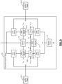
- FIG. 2 shows the optical transmitter 12 in further detail.
- the optical transmitter 12 comprises a power supply that generates all of the power supply voltages required by the components of the optical transmitter 12 (e.g., power supply voltages, bias voltages, and reference voltages described below).
- the DSP 20 receives digital data (bits) to be transmitted.
- the DSP 20 splits the data into multiple data streams of bits.
- Each of the serializers 22 serializes the bits in the respective data streams and outputs serial data.
- Each of the DACs 24 converts the serial data received from the respective serializer and outputs a current signal. The current signals from the DACs 24 are combined and input to the driver 26.
- the driver 26 converts the combined current signals output by the DACs 24 to a proportional voltage that can drive an external load (e.g., the optical fiber 16).
- the driver 26 generates a modulating signal based on the combined current signals output by the DACs 24.
- the driver 26 outputs the modulating signal to the optical modulator 30.
- the laser source 28 generates an optical signal (e.g., laser) that is used as a carrier by the transmitter 12 to transmit data.
- the optical modulator 30 modulates the optical signal with the modulating signal received from the driver 26 and generates a modulated optical signal.
- the transmitter 12 transmits the modulated optical signal via the optical fiber 16.
- FIGS. 3A and 3B show a design of the DACs 24.
- Each DAC 24 shown in FIG. 2 comprises the components shown in FIGS. 3A and 3B .
- each individual DAC 24 shown in FIG. 2 is referred to as the DAC 24.
- the following description applies to each of the DACs 24 shown in FIG. 2 .
- the DAC 24 comprises a timing circuit 50, circuitry 52, and DAC switches 54.
- the timing circuit 50 comprises a clock generator 60 and a phase control circuit 62.
- the circuitry 52 comprises a logic circuit 64 and a bias control circuit 66.
- the clock generator 60, the phase control circuit 62, and the bias control circuit 66 may be common to all the DACs 24 shown in FIG. 2 . That is, in some embodiments, only one clock generator 60, only one phase control circuit 62, and only one bias control circuit 66 may be used to drive all the DACs 24 shown in FIG. 2 .
- the DAC 24 is configured to convert digital data into analog data that is modulated by the optical modulator 30 (shown in FIG. 2 ) into an optical modulated signal for transmission over the optical fiber 16 (shown in FIG. 1 ).
- the timing circuit 50 is configured to generate timing signals to control the DAC switches 54.
- the clock generator 60 generates timing signals (e.g., clock signals) to control the DAC switches 54.
- the phase control circuit 62 controls a phase difference (shown at 70 in FIG. 5A ) between the clock signals to control an output data rate of the DAC 24. Accordingly, the timing circuit 50 generates the timing signals that include clock signals with a phase difference and adjusts the phase difference to control the output data rate of the DAC 24 as described below in further detail.
- the logic circuit 64 receives the clock signals output by the timing circuit 50 with a phase difference tuned (selected) by the phase control circuit 62 to achieve a desired output data rate of the DAC 24.
- the logic circuit 64 also receives the digital data D output by the respective serializer 22 (shown in FIG. 2 ).
- the circuitry 52 is configured to control the output data rate of the DAC 24 by biasing the DAC switches 54 based on a logical combination of the digital data and the timing signals as described below in further detail with reference to FIGS. 4A and 5A-5B .
- the DAC 24 By biasing the DAC switches 54 based on the logical combination of the digital data and the timing signals, the DAC 24 outputs analog data having a data rate that is greater than a data rate of the digital data. For example, by selecting a suitable phase difference between the clock signals used to drive the DAC switches 54, which is selected based on the desired output data rate of the DAC 24, the output data rate of the DAC 24 can be more (e.g., twice or even higher) than the data rate of the digital data.
- the DAC 24 By adjusting the phase difference of the timing signals using the phase control circuit 62, the DAC 24 outputs data at a data rate that is greater than the data rate of the digital data regardless of the pulse widths of the timing signals and a pulse width of the digital data.
- the phase difference between the clock signals can be tuned to scale the output data rate of the DAC 24. Controlling the output data rate of the DAC 24 by adjusting the phase difference of the timing signals relaxes timing constraints on the digital data and the timing signals. Accordingly, the output data rate of the DAC 24 can be scaled without imposing constraints on the timing (e.g., without narrowing pulse widths of) of the digital data and the timing signals.
- the DAC 24 outputs a current signal that is linear regardless of the output data rate of the DAC 24.
- the DAC 24 does not operate in voltage mode, where input and output of the DAC are synchronized voltage signals, and where achieving linearity of the DAC output at higher data rates is challenging as explained below.
- the DAC 24 operates in current mode using two series-connected switches (shown in FIG. 4A ), where the inputs (the digital data and the timing signals) to the DAC 24 are voltage signals but the output parameter of interest of the DAC 24 is a current signal of smaller pulse width compared to the input voltage signals.
- the current signal output by the DAC 24 varies linearly regardless of the output data rate of the DAC 24 and regardless of the pulse widths of the digital data and the timing signals as explained below.
- current mode has none of these limitations. This is because the output current of the DAC switches 54 is controlled by driving the DAC switches 54 using the logical combination of the digital data and the timing signals. By varying the phase difference of the timing signals, the logical combination of the digital data and the timing signals can vary the output current of the DAC 24 linearly regardless of the pulse widths of the digital data and the timing signals. Accordingly, unlike voltage mode, in current mode, the output current of the DAC 24 is independent of the pulse heights of the digital data and the timing signals (up to a certain limit).
- the pulse width of the output data of the DAC 24 can be varied linearly by adjusting the phase difference between the clock signals without regard to the pulse widths of the digital data and the timing signals and without increasing power supply voltage, which reduces power consumption. Accordingly, by operating the DAC 24 in current mode, driving the DAC 24 by the logical combination of the digital data and the timing signals, and controlling the phase difference between the clock signals, the output data rate of the DAC 24 can be increased linearly without increasing power consumption while relaxing the timing constraints on the inputs of the DAC 24.
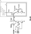
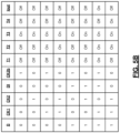
- FIGS. 4A-4B and 5A-5B show an example of implementation of the DAC 24 shown in FIGS. 3A and 3B .
- the DAC 24 comprises switches T1, T2, T3, and T4 (the DAC switches 54 shown in FIGS. 3A and 3B ); and a NAND gate (the circuitry 52 shown in FIGS. 3A and 3B ).
- the timing circuit 50 shown in FIGS. 3A and 3B generates the clock signals CK1 and CK2 shown in FIG. 5A .
- the clock generator 60 shown in FIG. 3B generates the clock signals CK1 and CK2, and the phase control circuit 62 shown in FIG. 3B controls the phase difference 70 between the clock signals CK1 and CK2 based on the desired output data rate of the DAC 24.
- the DAC 24 comprises the switches T1 and T2 connected to each other in series.
- the switches T3 and T4 are connected to the switch T1 at a node N as shown in FIG. 4A .
- the node N is called a source node since the node N is at a source terminal of the switch T1.
- the switch T3 is called a biasing switch, and the switch T4 is called a pullup switch. The operations of the switches T3 and T4 are described below.
- the NAND gate receives two inputs and receives an input as a power supply for the NAND gate.
- the two inputs to the NAND gate are the two clock signals CK1 and CK2 generated by the timing circuit 50 shown in FIGS. 3A and 3B .
- the digital data D output by the serializer 22 (shown in FIG. 2 ) is applied to the NAND gate as the power supply of the NAND gate.
- the NAND gate generates an output DI based on the two inputs CK1 and CK2 of the NAND gate and the digital data D, which is the power supply of the NAND gate.
- the bias control circuit 66 can control the bias voltage VB based on the swing requirements of the circuits following the driver 26 without compromising the performance provided by the DACs 24 and the driver 26.
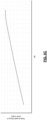
- the output swing of the driver 26 varies linearly with the bias voltage VB of the DACs 24 over an operating range.
- the performance of the driver 26 (e.g., including signal-to-ripple ratio) is insensitive to the swing amplitude (peak-to-peak output) of the driver 26.
Landscapes
- Physics & Mathematics (AREA)
- Engineering & Computer Science (AREA)
- Electromagnetism (AREA)
- Computer Networks & Wireless Communication (AREA)
- Signal Processing (AREA)
- Optics & Photonics (AREA)
- Theoretical Computer Science (AREA)
- Dc Digital Transmission (AREA)
- Optical Communication System (AREA)
Applications Claiming Priority (1)
| Application Number | Priority Date | Filing Date | Title |
|---|---|---|---|
| US202363609338P | 2023-12-12 | 2023-12-12 |
Publications (2)
| Publication Number | Publication Date |
|---|---|
| EP4583409A2 true EP4583409A2 (de) | 2025-07-09 |
| EP4583409A3 EP4583409A3 (de) | 2025-10-22 |
Family
ID=93923623
Family Applications (1)
| Application Number | Title | Priority Date | Filing Date |
|---|---|---|---|
| EP24219439.7A Pending EP4583409A3 (de) | 2023-12-12 | 2024-12-12 | Hochgeschwindigkeitssenderschaltung für optische übertragung |
Country Status (3)
| Country | Link |
|---|---|
| US (1) | US20250192890A1 (de) |
| EP (1) | EP4583409A3 (de) |
| CN (1) | CN120150837A (de) |
Family Cites Families (3)
| Publication number | Priority date | Publication date | Assignee | Title |
|---|---|---|---|---|
| EP3280074B1 (de) * | 2016-08-01 | 2018-11-14 | Knowledge Development for POF SL | Led-treiber für optische hochgeschwindigkeitskommunikation auf der basis linearer modulationen |
| US10951250B1 (en) * | 2019-05-29 | 2021-03-16 | Sitrus Technology Corporation | High-speed DC shifting predrivers with low ISI |
| US12111786B2 (en) * | 2020-11-09 | 2024-10-08 | Intel Corporation | Active inductor based high-bandwidth 2-state 4-way data serialization apparatus and method |
-
2024
- 2024-12-11 US US18/977,840 patent/US20250192890A1/en active Pending
- 2024-12-12 CN CN202411832053.XA patent/CN120150837A/zh active Pending
- 2024-12-12 EP EP24219439.7A patent/EP4583409A3/de active Pending
Also Published As
| Publication number | Publication date |
|---|---|
| CN120150837A (zh) | 2025-06-13 |
| EP4583409A3 (de) | 2025-10-22 |
| US20250192890A1 (en) | 2025-06-12 |
Similar Documents
| Publication | Publication Date | Title |
|---|---|---|
| US8669782B1 (en) | Active biasing in metal oxide semiconductor (MOS) differential pairs | |
| KR102279089B1 (ko) | 전압-모드 드라이버에 대한 임피던스 및 스윙 제어 | |
| US9130582B2 (en) | Systems and methods for correcting an offset at an output of a digital to analog converter | |
| US10110204B2 (en) | Low power buffer with gain boost | |
| US20060091955A1 (en) | Circuits and methods for improving slew rate of differential amplifiers | |
| CN101447785B (zh) | 差分驱动电路和通信设备 | |
| JP6585828B2 (ja) | ドライバ回路および光送信器 | |
| US7391264B2 (en) | Amplifier | |
| US7253685B2 (en) | Class AB amplifier having adjustable quiescent current and output current | |
| EP4115522B1 (de) | Architektur eines linearen transimpedanzverstärkers mit doppelregler und abstimmung | |
| Palermo et al. | High-speed transmitters in 90nm CMOS for high-density optical interconnects | |
| CN114756076B (zh) | 电压缓冲电路 | |
| US10298419B2 (en) | Low voltage differential signaling driver | |
| EP4583409A2 (de) | Hochgeschwindigkeitssenderschaltung für optische übertragung | |
| JP2010109512A (ja) | ドライバ回路及びドライバic | |
| US7053699B2 (en) | Current output stages | |
| US20060012433A1 (en) | Amplifier with a voltage-controlled quiescent current and output current | |
| US7342418B2 (en) | Low voltage differential signal receiver | |
| JP3759117B2 (ja) | I/v変換回路およびdaコンバータ | |
| US6798802B2 (en) | High-speed laser driver including wave-shaping circuits | |
| CN121077443B (zh) | H桥电路的驱动信号校准电路、数模转换器和发射机 | |
| JP3947085B2 (ja) | パルス幅調整回路 | |
| CN120377836A (zh) | 使用经调制信号修整电阻器 | |
| CN121193261A (zh) | 具有基于输出的校准的dac驱动器 |
Legal Events
| Date | Code | Title | Description |
|---|---|---|---|
| PUAI | Public reference made under article 153(3) epc to a published international application that has entered the european phase |
Free format text: ORIGINAL CODE: 0009012 |
|
| STAA | Information on the status of an ep patent application or granted ep patent |
Free format text: STATUS: THE APPLICATION HAS BEEN PUBLISHED |
|
| AK | Designated contracting states |
Kind code of ref document: A2 Designated state(s): AL AT BE BG CH CY CZ DE DK EE ES FI FR GB GR HR HU IE IS IT LI LT LU LV MC ME MK MT NL NO PL PT RO RS SE SI SK SM TR |
|
| PUAL | Search report despatched |
Free format text: ORIGINAL CODE: 0009013 |
|
| AK | Designated contracting states |
Kind code of ref document: A3 Designated state(s): AL AT BE BG CH CY CZ DE DK EE ES FI FR GB GR HR HU IE IS IT LI LT LU LV MC ME MK MT NL NO PL PT RO RS SE SI SK SM TR |
|
| RIC1 | Information provided on ipc code assigned before grant |
Ipc: H03M 1/74 20060101AFI20250912BHEP Ipc: H04B 10/50 20130101ALI20250912BHEP Ipc: H04B 10/40 20130101ALI20250912BHEP |
|
| STAA | Information on the status of an ep patent application or granted ep patent |
Free format text: STATUS: REQUEST FOR EXAMINATION WAS MADE |
|
| 17P | Request for examination filed |
Effective date: 20251021 |