EP4576574A1 - Systeme und verfahren zur leistungsschaltersteuerung für einen wechselrichter für ein elektrofahrzeug - Google Patents
Systeme und verfahren zur leistungsschaltersteuerung für einen wechselrichter für ein elektrofahrzeug Download PDFInfo
- Publication number
- EP4576574A1 EP4576574A1 EP24213611.7A EP24213611A EP4576574A1 EP 4576574 A1 EP4576574 A1 EP 4576574A1 EP 24213611 A EP24213611 A EP 24213611A EP 4576574 A1 EP4576574 A1 EP 4576574A1
- Authority
- EP
- European Patent Office
- Prior art keywords
- power switch
- voltage level
- gate voltage
- signal
- state
- Prior art date
- Legal status (The legal status is an assumption and is not a legal conclusion. Google has not performed a legal analysis and makes no representation as to the accuracy of the status listed.)
- Pending
Links
Images



Classifications
-
- H—ELECTRICITY
- H02—GENERATION; CONVERSION OR DISTRIBUTION OF ELECTRIC POWER
- H02P—CONTROL OR REGULATION OF ELECTRIC MOTORS, ELECTRIC GENERATORS OR DYNAMO-ELECTRIC CONVERTERS; CONTROLLING TRANSFORMERS, REACTORS OR CHOKE COILS
- H02P27/00—Arrangements or methods for the control of AC motors characterised by the kind of supply voltage
- H02P27/04—Arrangements or methods for the control of AC motors characterised by the kind of supply voltage using variable-frequency supply voltage, e.g. inverter or converter supply voltage
- H02P27/06—Arrangements or methods for the control of AC motors characterised by the kind of supply voltage using variable-frequency supply voltage, e.g. inverter or converter supply voltage using DC to AC converters or inverters
-
- H—ELECTRICITY
- H02—GENERATION; CONVERSION OR DISTRIBUTION OF ELECTRIC POWER
- H02M—APPARATUS FOR CONVERSION BETWEEN AC AND AC, BETWEEN AC AND DC, OR BETWEEN DC AND DC, AND FOR USE WITH MAINS OR SIMILAR POWER SUPPLY SYSTEMS; CONVERSION OF DC OR AC INPUT POWER INTO SURGE OUTPUT POWER; CONTROL OR REGULATION THEREOF
- H02M1/00—Details of apparatus for conversion
- H02M1/0003—Details of control, feedback or regulation circuits
- H02M1/0029—Circuits or arrangements for limiting the slope of switching signals, e.g. slew rate
-
- H—ELECTRICITY
- H02—GENERATION; CONVERSION OR DISTRIBUTION OF ELECTRIC POWER
- H02M—APPARATUS FOR CONVERSION BETWEEN AC AND AC, BETWEEN AC AND DC, OR BETWEEN DC AND DC, AND FOR USE WITH MAINS OR SIMILAR POWER SUPPLY SYSTEMS; CONVERSION OF DC OR AC INPUT POWER INTO SURGE OUTPUT POWER; CONTROL OR REGULATION THEREOF
- H02M1/00—Details of apparatus for conversion
- H02M1/0003—Details of control, feedback or regulation circuits
- H02M1/0038—Circuits or arrangements for suppressing, e.g. by masking incorrect turn-on or turn-off signals, e.g. due to current spikes in current mode control
-
- H—ELECTRICITY
- H02—GENERATION; CONVERSION OR DISTRIBUTION OF ELECTRIC POWER
- H02M—APPARATUS FOR CONVERSION BETWEEN AC AND AC, BETWEEN AC AND DC, OR BETWEEN DC AND DC, AND FOR USE WITH MAINS OR SIMILAR POWER SUPPLY SYSTEMS; CONVERSION OF DC OR AC INPUT POWER INTO SURGE OUTPUT POWER; CONTROL OR REGULATION THEREOF
- H02M1/00—Details of apparatus for conversion
- H02M1/08—Circuits specially adapted for the generation of control voltages for semiconductor devices incorporated in static converters
-
- H—ELECTRICITY
- H02—GENERATION; CONVERSION OR DISTRIBUTION OF ELECTRIC POWER
- H02M—APPARATUS FOR CONVERSION BETWEEN AC AND AC, BETWEEN AC AND DC, OR BETWEEN DC AND DC, AND FOR USE WITH MAINS OR SIMILAR POWER SUPPLY SYSTEMS; CONVERSION OF DC OR AC INPUT POWER INTO SURGE OUTPUT POWER; CONTROL OR REGULATION THEREOF
- H02M1/00—Details of apparatus for conversion
- H02M1/32—Means for protecting converters other than automatic disconnection
-
- H—ELECTRICITY
- H02—GENERATION; CONVERSION OR DISTRIBUTION OF ELECTRIC POWER
- H02M—APPARATUS FOR CONVERSION BETWEEN AC AND AC, BETWEEN AC AND DC, OR BETWEEN DC AND DC, AND FOR USE WITH MAINS OR SIMILAR POWER SUPPLY SYSTEMS; CONVERSION OF DC OR AC INPUT POWER INTO SURGE OUTPUT POWER; CONTROL OR REGULATION THEREOF
- H02M7/00—Conversion of AC power input into DC power output; Conversion of DC power input into AC power output
- H02M7/42—Conversion of DC power input into AC power output without possibility of reversal
- H02M7/44—Conversion of DC power input into AC power output without possibility of reversal by static converters
- H02M7/48—Conversion of DC power input into AC power output without possibility of reversal by static converters using discharge tubes with control electrode or semiconductor devices with control electrode
- H02M7/53—Conversion of DC power input into AC power output without possibility of reversal by static converters using discharge tubes with control electrode or semiconductor devices with control electrode using devices of a triode or transistor type requiring continuous application of a control signal
- H02M7/537—Conversion of DC power input into AC power output without possibility of reversal by static converters using discharge tubes with control electrode or semiconductor devices with control electrode using devices of a triode or transistor type requiring continuous application of a control signal using semiconductor devices only, e.g. single switched pulse inverters
- H02M7/5387—Conversion of DC power input into AC power output without possibility of reversal by static converters using discharge tubes with control electrode or semiconductor devices with control electrode using devices of a triode or transistor type requiring continuous application of a control signal using semiconductor devices only, e.g. single switched pulse inverters in a bridge configuration
-
- H—ELECTRICITY
- H02—GENERATION; CONVERSION OR DISTRIBUTION OF ELECTRIC POWER
- H02M—APPARATUS FOR CONVERSION BETWEEN AC AND AC, BETWEEN AC AND DC, OR BETWEEN DC AND DC, AND FOR USE WITH MAINS OR SIMILAR POWER SUPPLY SYSTEMS; CONVERSION OF DC OR AC INPUT POWER INTO SURGE OUTPUT POWER; CONTROL OR REGULATION THEREOF
- H02M7/00—Conversion of AC power input into DC power output; Conversion of DC power input into AC power output
- H02M7/42—Conversion of DC power input into AC power output without possibility of reversal
- H02M7/44—Conversion of DC power input into AC power output without possibility of reversal by static converters
- H02M7/48—Conversion of DC power input into AC power output without possibility of reversal by static converters using discharge tubes with control electrode or semiconductor devices with control electrode
- H02M7/53—Conversion of DC power input into AC power output without possibility of reversal by static converters using discharge tubes with control electrode or semiconductor devices with control electrode using devices of a triode or transistor type requiring continuous application of a control signal
- H02M7/537—Conversion of DC power input into AC power output without possibility of reversal by static converters using discharge tubes with control electrode or semiconductor devices with control electrode using devices of a triode or transistor type requiring continuous application of a control signal using semiconductor devices only, e.g. single switched pulse inverters
- H02M7/5387—Conversion of DC power input into AC power output without possibility of reversal by static converters using discharge tubes with control electrode or semiconductor devices with control electrode using devices of a triode or transistor type requiring continuous application of a control signal using semiconductor devices only, e.g. single switched pulse inverters in a bridge configuration
- H02M7/53871—Conversion of DC power input into AC power output without possibility of reversal by static converters using discharge tubes with control electrode or semiconductor devices with control electrode using devices of a triode or transistor type requiring continuous application of a control signal using semiconductor devices only, e.g. single switched pulse inverters in a bridge configuration with automatic control of output voltage or current
- H02M7/53873—Conversion of DC power input into AC power output without possibility of reversal by static converters using discharge tubes with control electrode or semiconductor devices with control electrode using devices of a triode or transistor type requiring continuous application of a control signal using semiconductor devices only, e.g. single switched pulse inverters in a bridge configuration with automatic control of output voltage or current with digital control
-
- H—ELECTRICITY
- H02—GENERATION; CONVERSION OR DISTRIBUTION OF ELECTRIC POWER
- H02P—CONTROL OR REGULATION OF ELECTRIC MOTORS, ELECTRIC GENERATORS OR DYNAMO-ELECTRIC CONVERTERS; CONTROLLING TRANSFORMERS, REACTORS OR CHOKE COILS
- H02P27/00—Arrangements or methods for the control of AC motors characterised by the kind of supply voltage
- H02P27/04—Arrangements or methods for the control of AC motors characterised by the kind of supply voltage using variable-frequency supply voltage, e.g. inverter or converter supply voltage
- H02P27/06—Arrangements or methods for the control of AC motors characterised by the kind of supply voltage using variable-frequency supply voltage, e.g. inverter or converter supply voltage using DC to AC converters or inverters
- H02P27/08—Arrangements or methods for the control of AC motors characterised by the kind of supply voltage using variable-frequency supply voltage, e.g. inverter or converter supply voltage using DC to AC converters or inverters with pulse width modulation
-
- H—ELECTRICITY
- H03—ELECTRONIC CIRCUITRY
- H03K—PULSE TECHNIQUE
- H03K17/00—Electronic switching or gating, i.e. not by contact-making and –breaking
- H03K17/04—Modifications for accelerating switching
- H03K17/041—Modifications for accelerating switching without feedback from the output circuit to the control circuit
- H03K17/04106—Modifications for accelerating switching without feedback from the output circuit to the control circuit in field-effect transistor switches
-
- H—ELECTRICITY
- H03—ELECTRONIC CIRCUITRY
- H03K—PULSE TECHNIQUE
- H03K17/00—Electronic switching or gating, i.e. not by contact-making and –breaking
- H03K17/12—Modifications for increasing the maximum permissible switched current
- H03K17/122—Modifications for increasing the maximum permissible switched current in field-effect transistor switches
-
- H—ELECTRICITY
- H03—ELECTRONIC CIRCUITRY
- H03K—PULSE TECHNIQUE
- H03K17/00—Electronic switching or gating, i.e. not by contact-making and –breaking
- H03K17/16—Modifications for eliminating interference voltages or currents
- H03K17/161—Modifications for eliminating interference voltages or currents in field-effect transistor switches
- H03K17/162—Modifications for eliminating interference voltages or currents in field-effect transistor switches without feedback from the output circuit to the control circuit
-
- H—ELECTRICITY
- H02—GENERATION; CONVERSION OR DISTRIBUTION OF ELECTRIC POWER
- H02M—APPARATUS FOR CONVERSION BETWEEN AC AND AC, BETWEEN AC AND DC, OR BETWEEN DC AND DC, AND FOR USE WITH MAINS OR SIMILAR POWER SUPPLY SYSTEMS; CONVERSION OF DC OR AC INPUT POWER INTO SURGE OUTPUT POWER; CONTROL OR REGULATION THEREOF
- H02M1/00—Details of apparatus for conversion
- H02M1/0048—Circuits or arrangements for reducing losses
- H02M1/0054—Transistor switching losses
Definitions
- Various embodiments of the present disclosure relate generally to systems and methods for one or more controllers for a power switch, and, more particularly, to systems and methods for controlling a gate driver for a power switch for an inverter for an electric vehicle.
- Inverters such as those used to drive a motor in an electric vehicle, for example, are responsible for converting High Voltage Direct Current (HVDC) into Alternating Current (AC) to drive the motor.
- HVDC High Voltage Direct Current
- AC Alternating Current
- switching losses of a power device switch can contribute to the inefficiencies of the inverter.
- the techniques described herein relate to a system including: an inverter configured to convert DC power from a battery to AC power to drive a motor, wherein the inverter includes: a power switch including a gate terminal; and a gate driver configured to: receive a pulse to control an operation of the power switch, generate, based on the received pulse, a first signal to the gate terminal to increase a gate voltage level of the power switch at a first rate from an off-state gate voltage level to a first on-state gate voltage level in a first time period, and generate, based on the received pulse, a second signal to the gate terminal to increase the gate voltage level of the power switch at a second rate, less than the first rate, to a second on-state gate voltage level in a second time period subsequent to the first time period.
- the techniques described herein relate to a system, wherein the gate driver is further configured to: generate, based on the received pulse, a third signal to the gate terminal to decrease the gate voltage level of the power switch from the first on-state gate voltage level to a third on-state gate voltage level, lower than the first on-state gate voltage level, in a third time period subsequent to the first time period and preceding the second time period.
- the techniques described herein relate to a system, wherein the second signal is configured to increase the gate voltage level of the power switch from the third on-state gate voltage level to the second on-state gate voltage level.
- the techniques described herein relate to a system, wherein the third signal is configured to cause the power switch to decrease to the third on-state gate voltage level to avoid an overshoot of the gate voltage level of the power switch above a maximum rated gate voltage level of the power switch.
- the techniques described herein relate to a system, wherein the gate driver is further configured to: generate, based on the received pulse, a fourth signal to the gate terminal to decrease the gate voltage level of the power switch from the second on-state gate voltage level to the off-state gate voltage level in a fourth time period subsequent to the second time period.
- the techniques described herein relate to a system, further including: the battery configured to supply the DC power to the inverter; and the motor configured to receive the AC power from the inverter to drive the motor.
- the techniques described herein relate to a system, further including: an electric vehicle including the battery, the inverter, and the motor.
- the techniques described herein relate to a system including: a power switch driver configured to: receive a pulse to control an operation of a power switch, generate, based on the received pulse, a first signal to the power switch to increase a gate voltage level of the power switch at a first rate from an off-state gate voltage level to a first on-state gate voltage level in a first time period, and generate, based on the received pulse, a second signal to the power switch to increase the gate voltage level of the power switch at a second rate, less than the first rate, to a second on-state gate voltage level in a second time period subsequent to the first time period.
- the techniques described herein relate to a system, wherein: the first rate is at least 22V/1 ⁇ s, and the second rate is approximately 3V/8 ⁇ s.
- the techniques described herein relate to a system, wherein the power switch driver is an external waveform controller for a gate driver.
- the techniques described herein relate to a system, wherein the power switch driver includes one or more power supplies to generate one or more of the first signal or the second signal.
- the techniques described herein relate to a system, wherein the power switch driver includes one or more switches to generate one or more of the first signal or the second signal.
- the techniques described herein relate to a system, wherein the power switch driver includes one or more diodes to control flow of current from an external power supply.
- the techniques described herein relate to a system, wherein the power switch driver includes one or more resistors to control the first rate and the second rate.
- the techniques described herein relate to a system including: a gate driver configured to receive a pulse to control an operation of a power switch, and generate a gate signal based on the pulse; and a waveform controller configured to: receive the gate signal from the gate driver, generate, based on the received gate signal, a first signal to the power switch to increase a gate voltage level of the power switch at a first rate from an off-state gate voltage level to a first on-state gate voltage level in a first time period, and generate, based on the received gate signal, a second signal to the power switch to increase the gate voltage level of the power switch at a second rate, less than the first rate, to a second on-state gate voltage level in a second time period subsequent to the first time period.
- the techniques described herein relate to a system, wherein the waveform controller includes one or more electrical hardware components to control a time delay between an initial rise in the gate voltage level of the power switch to the first on-state gate voltage level and a subsequent rise in the gate voltage level of the power switch to the second on-state gate voltage level.
- the techniques described herein relate to a system, wherein the waveform controller includes one or more electrical hardware components to control the second rate.
- the techniques described herein relate to a method including performing, by one or more controllers, operations including: receiving a pulse to control an operation of a power switch including a gate terminal; generating, based on the received pulse, a first signal to the gate terminal to increase a gate voltage level of the power switch at a first rate from an off-state gate voltage level to a first on-state gate voltage level in a first time period; and generating, based on the received pulse, a second signal to the gate terminal to increase the gate voltage level of the power switch at a second rate, less than the first rate, to a second on-state gate voltage level in a second time period subsequent to the first time period.
- the techniques described herein relate to a method, wherein the first rate is configured to cause the power switch to transition from the off-state gate voltage level to the first on-state gate voltage level in less than 1 ⁇ s.
- the techniques described herein relate to a method, wherein the second time period is subsequent to a settling of a ringing phase at the gate terminal of the power switch, wherein the ringing phase is caused by the generated first signal.
- the techniques described herein relate to a method, wherein the second rate is configured to cause the power switch to increase to the second on-state gate voltage level with reduced oscillations relative to oscillations of the gate voltage level of the power switch in the first time period.
- the techniques described herein relate to a method, wherein the operations further include: generating, based on the received pulse, a third signal to the gate terminal to decrease the gate voltage level of the power switch from the first on-state gate voltage level to a third on-state gate voltage level, lower than the first on-state gate voltage level, in a third time period subsequent to the first time period and preceding the second time period.
- the techniques described herein relate to a method, wherein the second signal is configured to increase the gate voltage level of the power switch from the third on-state gate voltage level to the second on-state gate voltage level.
- the techniques described herein relate to a method, wherein the third signal is configured to cause the power switch to decrease to the third on-state gate voltage level to avoid an overshoot of the gate voltage level of the power switch above a maximum rated gate voltage level of the power switch.
- the techniques described herein relate to a method, wherein the operations further include: generating, based on the received pulse, a fourth signal to the gate terminal to decrease the gate voltage level of the power switch from the second on-state gate voltage level to the off-state gate voltage level in a fourth time period subsequent to the second time period.
- the techniques described herein relate to a method, further including: receiving DC power from a battery; converting the DC power to AC power using the operation of the power switch; and providing the AC power to a motor.
- the techniques described herein relate to a method, wherein: the one or more controllers, the power switch, the battery, and the motor are provided as a system in an electric vehicle.
- the techniques described herein relate to a method including performing, by one or more controllers, operations including: receiving a pulse to control an operation of a power switch; generating, based on the received pulse, a first signal to the power switch to increase a gate voltage level of the power switch at a first rate from an off-state gate voltage level to a first on-state gate voltage level in a first time period, and generating, based on the received pulse, a second signal to the power switch to increase the gate voltage level of the power switch at a second rate, less than the first rate, to a second on-state gate voltage level in a second time period subsequent to the first time period.
- the techniques described herein relate to a method, wherein: the first rate is configured to cause the power switch to transition from the off-state gate voltage level to the first on-state gate voltage level in less than 1 ⁇ s, and the second rate is configured to cause the power switch to increase to the second on-state gate voltage level with reduced oscillations relative to oscillations of the gate voltage level of the power switch in the first time period.
- the techniques described herein relate to a method, wherein the second time period is subsequent to a settled ringing phase of the power switch, wherein the ringing phase is caused by the generated first signal.
- the techniques described herein relate to a method, wherein the operations further include: generating, based on the received pulse, a third signal to the power switch to decrease the gate voltage level of the power switch from the first on-state gate voltage level to a third on-state gate voltage level, lower than the first on-state gate voltage level, in a third time period subsequent to the first time period and preceding the second time period.
- the techniques described herein relate to a method, wherein the second signal is configured to increase the gate voltage level of the power switch from the third on-state gate voltage level to the second on-state gate voltage level.
- the techniques described herein relate to a method, wherein the third signal is configured to cause the power switch to decrease to the third on-state gate voltage level to avoid an overshoot of the gate voltage level of the power switch above a maximum rated gate voltage level of the power switch.
- the techniques described herein relate to a method, wherein the operations further include: generating, based on the received pulse, a fourth signal to the power switch to decrease the gate voltage level of the power switch from the second on-state gate voltage level to the off-state gate voltage level in a fourth time period subsequent to the second time period.
- the techniques described herein relate to a method including performing, by one or more controllers, operations including: receiving a pulse to control an operation of a power switch; generating a gate signal based on the pulse; generating, based on the received gate signal, a first signal to the power switch to increase a gate voltage level of the power switch at a first rate from an off-state gate voltage level to a first on-state gate voltage level in a first time period; and generating, based on the received gate signal, a second signal to the power switch to increase the gate voltage level of the power switch at a second rate, less than the first rate, to a second on-state gate voltage level in a second time period subsequent to the first time period.
- the techniques described herein relate to a method, wherein: the first rate is configured to cause the power switch to transition from the off-state gate voltage level to the first on-state gate voltage level in less than 1 ⁇ s, and the second rate is configured to cause the power switch to increase to the second on-state gate voltage level with reduced oscillations relative to oscillations of the gate voltage level of the power switch in the first time period.
- the techniques described herein relate to a method, wherein the operations further include: generating, based on the received gate signal, a third signal to the power switch to decrease the gate voltage level of the power switch from the first on-state gate voltage level to a third on-state gate voltage level, lower than the first on-state gate voltage level, in a third time period subsequent to the first time period and preceding the second time period.
- switches may be described as switches or devices, but may refer to any device for controlling the flow of power in an electrical circuit.
- switches may be metal-oxide-semiconductor field-effect transistors (MOSFETs), bipolar junction transistors (BJTs), insulated-gate bipolar transistors (IGBTs), or relays, for example, or any combination thereof, but are not limited thereto.
- MOSFETs metal-oxide-semiconductor field-effect transistors
- BJTs bipolar junction transistors
- IGBTs insulated-gate bipolar transistors
- Various embodiments of the present disclosure relate generally to systems and methods for one or more controllers for a power switch, and, more particularly, to systems and methods for controlling a gate driver for a power switch for an inverter for an electric vehicle.
- a three phase inverter may include a bridge with six power device switches (for example, power transistors such as IGBT or MOSFET) that are controlled by Pulse Width Modulation (PWM) signals generated by a controller.
- An inverter may include three phase switch groups, (e.g. six power switches) to control the phase voltage, upper and lower gate drivers to control the switches, and a PWM controller to control the gate drivers.
- the PWM controller may generate signals to define the intended states of the system.
- the gate drivers may send the amplified signals from the PWM controller to the phase switches.
- the phase switches may drive the phase voltage.
- a power module may be an important component of the overall system, and an efficiency of the system may be directly proportional to losses occurring in the power module. Addressing switching losses and conduction losses of the power module may be necessary for an efficient, cost-effective, and robust inverter design. One or more embodiments may reduce switching and conduction losses.
- a gate of a MOSFET is turned on with a fixed gate voltage. Therefore, the gate sourcing current is limited by gate resistance only. A fixed gate voltage does not allow a reduction of an on-state resistance of the MOSFET.
- Some solutions address this limitation by using a current-controlled gate driver to control the gate sourcing current of the MOSFET.
- Some solutions use a gate voltage margin to maximum limit (Vgs max) based on oscillations and dynamic behavior.
- Vgs max gate voltage margin to maximum limit
- a power switch may be controlled by gate-to-source voltage (Vgs).
- Vgs gate-to-source voltage
- a negative Vgs may transition the power switch to an off, or open, state
- a positive Vgs may transition the power switch to an on, or closed, state.
- the positive, or turn-on, Vgs is limited to a value below a maximum positive Vgs for the power switch to maintain dynamic voltages within a safety margin for the power switch to avoid failure of the power switch.
- the negative, or turn-off, Vgs is limited to a value above a maximum negative Vgs for the power switch.
- a power switch having a maximum rating from -8V to 19V may have a turn-off Vgs of -4V and a turn-on Vgs of 15V.
- Switching losses in the power switch are dependent on a switching speed of the power switch, such as a loss in a turn-on transition of the power switch. Turning the power switch on more quickly will decrease this turn-on loss.
- One or more embodiments may include a system to turn on a power switch with an initial Vgs having a first value, reduce the Vgs from the first value to a second value in a ringing phase, and increase the Vgs from the second value to a third value after the ringing phase.
- the first value for the Vgs may be 18V
- the second value may be 15V
- the third value may be 18V.
- the initial Vgs may quickly, at a first rate, transition the power switch from an off state to an on state, which, if not mitigated, may introduce excessive oscillations, or ringing, in the power switch.
- the 18V initial Vgs is maintained during the ringing phase, the power switch may overshoot a maximum current rating of the switch, which may damage the power switch.
- one or more embodiments may reduce the initial Vgs (e.g. 18V) to a second value (e.g. 15V) during the ringing phase of the power switch subsequent to the initial turn-on. Reducing the initial Vgs to the second value may avoid exceeding a rated gate voltage of the power switch during the ringing phase.
- a voltage level at the output of gate driver may be higher than a MOSFET gate voltage capability. Accordingly, a gate voltage may be reduced due to a static gate voltage limit and to avoid exceeding the limit during ringing.
- the reduced Vgs also increases the on-state resistance of the power switch, which may increase a junction temperature of the power switch and/or increase a conduction loss of the power switch.
- one or more embodiments may slowly increase, at a second rate less than the first rate, the Vgs to a third value (e.g. 18V) higher than the second value (e.g. 15V).
- the slow increase to the third value may limit dynamics in the complete inverter/converter system.
- the increased Vgs may reduce the on-state resistance of the power switch, which may decrease (or avoid an increase in) a junction temperature of the power switch and/or decrease a conduction loss of the power switch.
- the first value may be less than, the same as, or greater than a maximum Vgs of the power switch.
- the second value may be less than the first value.
- the third value may be greater than the second value, and may be less than, the same as, or greater than the first value.
- One or more embodiments may decrease a switching loss of the power switch with a first high Vgs.
- One or more embodiments may avoid exceeding a rated gate voltage during a ringing phase of the power switch with a second lower Vgs.
- a voltage level at the output of gate driver may be higher than a MOSFET gate voltage capability. Accordingly, a gate voltage may be reduced due to a static gate voltage limit and to avoid exceeding the limit during ringing.
- One or more embodiments may decrease a conduction loss of the power switch with a third higher Vgs.
- One or more embodiments may limit dynamics, such as additional ringing of the power switch, during the transition from the second lower Vgs to the third higher Vgs with a ramped Vgs.
- one or more embodiments may apply a higher gate voltage.
- the gate voltage may then be reduced to avoid exceeding a rated gate voltage.
- a voltage level at the output of gate driver may be higher than a MOSFET gate voltage capability. Accordingly, a gate voltage may be reduced due to a static gate voltage limit and to avoid exceeding the limit during ringing.
- one or more embodiments may increase the gate voltage to reduce an on-state resistance (Rdson) of the power switch.
- Rdson on-state resistance
- One or more embodiments may increase the gate voltage slowly to avoid further ringing in the circuit. Due to the increased gate voltage, a conduction loss in the power switch will decrease.
- One or more embodiments may provide a gate signal pattern that increases a gate voltage after ringing (following an initial turn-on of a power switch).
- One or more embodiments may provide a power level signal pattern for one or more Si MOSFET, SiC MOSFET, IGBT, or GaN devices, for example.
- a power level may refer to an output signal from a gate driver.
- a power level may be a gate voltage level, for example.
- One or more embodiments may apply a higher gate voltage to charge the gate faster.
- One or more embodiments may reduce the gate voltage to avoid exceeding a rated gate voltage.
- a voltage level at the output of gate driver may be higher than a MOSFET gate voltage capability. Accordingly, a gate voltage may be reduced due to a static gate voltage limit and to avoid exceeding the limit during ringing.
- One or more embodiments may increase the gate voltage to a higher voltage to reduce on-state resistance when the ringing subsides.
- One or more embodiments may provide a fast turn-on power switch without an increase in ringing.
- One or more embodiments may provide a reduced on-state resistance, reduced conduction loss, and reduced junction temperature.
- One or more embodiments may provide a reduced substrate size and reduction in a cost and overall size of the power module, due to the reduced junction temperature.
- FIG. 1 depicts an exemplary system infrastructure for a vehicle including a combined inverter and converter, according to one or more embodiments.
- the combined inverter and converter may be referred to as an inverter.
- electric vehicle 100 may include an inverter 110, a motor 190, and a battery 195.
- the inverter 110 may include components to receive electrical power from an external source and output electrical power to charge battery 195 of electric vehicle 100.
- the inverter 110 may convert DC power from battery 195 in electric vehicle 100 to AC power, to drive motor 190 of the electric vehicle 100, for example, but the embodiments are not limited thereto.
- the inverter 110 may be bidirectional, and may convert DC power to AC power, or convert AC power to DC power, such as during regenerative braking, for example.
- Inverter 110 may be a three-phase inverter, a single-phase inverter, or a multi-phase inverter.
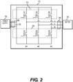
- FIG. 2 depicts an electrical power schematic of a three phase inverter module, according to one or more embodiments.
- inverter 110 may be connected to a battery, or power supply, 195 and a motor, or load, 190.
- Inverter 110 may include first three-phase switch group 210, and second three-phase switch group 220.
- a first phase U may correlate with ⁇ A including switches Q1 and Q4, a second phase V may correlate with ⁇ B including switches Q3 and Q6, and a third phase W may correlate with ⁇ C including switches Q5 and Q2, as illustrated in FIG. 2 .
- First three-phase switch group 210 may include first phase switch Q1, second phase switch Q3, and third phase switch Q5.
- Second three-phase switch group 220 may include first phase switch Q4, second phase switch Q6, and third phase switch Q2.
- Switches Q1-Q6 may be metal-oxide-semiconductor field-effect transistors (MOSFET), for example, but are not limited thereto.
- MOSFET metal-oxide-semiconductor field-effect transistors
- the first three-phase switch group 210 and second three-phase switch group 220 may be driven by a PWM signal (as illustrated, for example, in FIGS. 5 , 7 , and 9 ) generated by inverter controller 300 to convert DC power delivered via input terminal set 285 at capacitor 230 to three phase AC power at outputs U, V, and W via output terminal set 295 to motor 190.
- a PWM signal as illustrated, for example, in FIGS. 5 , 7 , and 9
- FIGS. 1 and 2 illustrate a three-phase inverter, the disclosure is not limited thereto, and may include single phase or multi-phase inverters.
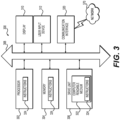
- FIG. 3 depicts an exemplary system infrastructure for inverter controller 300 of FIG. 2 , according to one or more embodiments.
- Inverter controller 300 may include one or more controllers.
- the inverter controller 300 may include a set of instructions that can be executed to cause the inverter controller 300 to perform any one or more of the methods or computer based functions disclosed herein.
- the inverter controller 300 may operate as a standalone device or may be connected, e.g., using a network, to other computer systems or peripheral devices.
- the inverter controller 300 may operate in the capacity of a server or as a client in a server-client user network environment, or as a peer computer system in a peer-to-peer (or distributed) network environment.
- the inverter controller 300 can also be implemented as or incorporated into various devices, such as inverter 110 in electric vehicle 100, a personal computer (PC), a tablet PC, a set-top box (STB), a personal digital assistant (PDA), a mobile device, a palmtop computer, a laptop computer, a desktop computer, a communications device, a wireless telephone, a land-line telephone, a control system, a camera, a scanner, a facsimile machine, a printer, a pager, a personal trusted device, a web appliance, a network router, switch or bridge, or any other machine capable of executing a set of instructions (sequential or otherwise) that specify actions to be taken by that machine.
- PC personal computer
- PDA personal digital assistant
- STB set-top box
- the inverter controller 300 can be implemented using electronic devices that provide voice, video, or data communication. Further, while the inverter controller 300 is illustrated as a single system, the term "system” shall also be taken to include any collection of systems or sub-systems that individually or jointly execute a set, or multiple sets, of instructions to perform one or more computer functions.
- the inverter controller 300 may include a processor 302, e.g., a central processing unit (CPU), a graphics processing unit (GPU), or both.
- the processor 302 may be a component in a variety of systems.
- the processor 302 may be part of a standard inverter.
- the processor 302 may be one or more general processors, digital signal processors, application specific integrated circuits, field programmable gate arrays, servers, networks, digital circuits, analog circuits, combinations thereof, or other now known or later developed devices for analyzing and processing data.
- the processor 302 may implement a software program, such as code generated manually (i.e., programmed).
- the inverter controller 300 may include a memory 304 that can communicate via a bus 308.
- the memory 304 may be a main memory, a static memory, or a dynamic memory.
- the memory 304 may include, but is not limited to computer readable storage media such as various types of volatile and non-volatile storage media, including but not limited to random access memory, read-only memory, programmable read-only memory, electrically programmable read-only memory, electrically erasable read-only memory, flash memory, magnetic tape or disk, optical media and the like.
- the memory 304 includes a cache or random-access memory for the processor 302.
- the memory 304 is separate from the processor 302, such as a cache memory of a processor, the system memory, or other memory.
- the memory 304 may be an external storage device or database for storing data. Examples include a hard drive, compact disc (“CD”), digital video disc (“DVD”), memory card, memory stick, floppy disc, universal serial bus (“USB”) memory device, or any other device operative to store data.
- the memory 304 is operable to store instructions executable by the processor 302.
- the functions, acts or tasks illustrated in the figures or described herein may be performed by the processor 302 executing the instructions stored in the memory 304.
- the functions, acts or tasks are independent of the particular type of instructions set, storage media, processor or processing strategy and may be performed by software, hardware, integrated circuits, firmware, micro-code and the like, operating alone or in combination.
- processing strategies may include multiprocessing, multitasking, parallel processing and the like.
- the inverter controller 300 may further include a display 310, such as a liquid crystal display (LCD), an organic light emitting diode (OLED), a flat panel display, a solid-state display, a cathode ray tube (CRT), a projector, a printer or other now known or later developed display device for outputting determined information.
- a display 310 such as a liquid crystal display (LCD), an organic light emitting diode (OLED), a flat panel display, a solid-state display, a cathode ray tube (CRT), a projector, a printer or other now known or later developed display device for outputting determined information.
- the display 310 may act as an interface for the user to see the functioning of the processor 302, or specifically as an interface with the software stored in the memory 304 or in the drive unit 306.
- the inverter controller 300 may include an input device 312 configured to allow a user to interact with any of the components of inverter controller 300.
- the input device 312 may be a number pad, a keyboard, or a cursor control device, such as a mouse, or a joystick, touch screen display, remote control, or any other device operative to interact with the inverter controller 300.
- the inverter controller 300 may also or alternatively include drive unit 306 implemented as a disk or optical drive.
- the drive unit 306 may include a computer-readable medium 322 in which one or more sets of instructions 324, e.g. software, can be embedded. Further, the instructions 324 may embody one or more of the methods or logic as described herein. The instructions 324 may reside completely or partially within the memory 304 and/or within the processor 302 during execution by the inverter controller 300.
- the memory 304 and the processor 302 also may include computer-readable media as discussed above.
- a computer-readable medium 322 includes instructions 324 or receives and executes instructions 324 responsive to a propagated signal so that a device connected to a network 370 can communicate voice, video, audio, images, or any other data over the network 370. Further, the instructions 324 may be transmitted or received over the network 370 via a communication port or interface 320, and/or using a bus 308.
- the communication port or interface 320 may be a part of the processor 302 or may be a separate component.
- the communication port or interface 320 may be created in software or may be a physical connection in hardware.
- the communication port or interface 320 may be configured to connect with a network 370, external media, the display 310, or any other components in inverter controller 300, or combinations thereof.
- connection with the network 370 may be a physical connection, such as a wired Ethernet connection or may be established wirelessly as discussed below.
- additional connections with other components of the inverter controller 300 may be physical connections or may be established wirelessly.
- the network 370 may alternatively be directly connected to a bus 308.
- While the computer-readable medium 322 is shown to be a single medium, the term “computer-readable medium” may include a single medium or multiple media, such as a centralized or distributed database, and/or associated caches and servers that store one or more sets of instructions.
- the term “computer-readable medium” may also include any medium that is capable of storing, encoding, or carrying a set of instructions for execution by a processor or that cause a computer system to perform any one or more of the methods or operations disclosed herein.
- the computer-readable medium 322 may be non-transitory, and may be tangible.
- the computer-readable medium 322 can include a solid-state memory such as a memory card or other package that houses one or more non-volatile read-only memories.
- the computer-readable medium 322 can be a random-access memory or other volatile re-writable memory. Additionally or alternatively, the computer-readable medium 322 can include a magneto-optical or optical medium, such as a disk or tapes or other storage device to capture carrier wave signals such as a signal communicated over a transmission medium.
- a digital file attachment to an e-mail or other self-contained information archive or set of archives may be considered a distribution medium that is a tangible storage medium. Accordingly, the disclosure is considered to include any one or more of a computer-readable medium or a distribution medium and other equivalents and successor media, in which data or instructions may be stored.
- dedicated hardware implementations such as application specific integrated circuits, programmable logic arrays and other hardware devices, can be constructed to implement one or more of the methods described herein.
- Applications that may include the apparatus and systems of various implementations can broadly include a variety of electronic and computer systems.
- One or more implementations described herein may implement functions using two or more specific interconnected hardware modules or devices with related control and data signals that can be communicated between and through the modules, or as portions of an application-specific integrated circuit. Accordingly, the present system encompasses software, firmware, and hardware implementations.
- the inverter controller 300 may be connected to a network 370.
- the network 370 may define one or more networks including wired or wireless networks.
- the wireless network may be a cellular telephone network, an 802.11, 802.16, 802.20, or WiMAX network.
- such networks may include a public network, such as the Internet, a private network, such as an intranet, or combinations thereof, and may utilize a variety of networking protocols now available or later developed including, but not limited to TCP/IP based networking protocols.
- the network 370 may include wide area networks (WAN), such as the Internet, local area networks (LAN), campus area networks, metropolitan area networks, a direct connection such as through a Universal Serial Bus (USB) port, or any other networks that may allow for data communication.
- WAN wide area networks
- LAN local area networks
- USB Universal Serial Bus
- the network 370 may be configured to couple one computing device to another computing device to enable communication of data between the devices.
- the network 370 may generally be enabled to employ any form of machine-readable media for communicating information from one device to another.
- the network 370 may include communication methods by which information may travel between computing devices.
- the network 370 may be divided into sub-networks. The sub-networks may allow access to all of the other components connected thereto or the sub-networks may restrict access between the components.
- the network 370 may be regarded as a public or private network connection and may include, for example, a virtual private network or an encryption or other security mechanism employed over the public Internet, or the like.
- the methods described herein may be implemented by software programs executable by a computer system.
- implementations can include distributed processing, component or object distributed processing, and parallel processing.
- virtual computer system processing can be constructed to implement one or more of the methods or functionality as described herein.
- FIG. 4 depicts a power switch control system, according to one or more embodiments.
- gate driver system 400 may include gate driver 450 and power switch 420.
- Gate driver 450 may receive a pulse width modulation signal as PWM signal 405 from an external source, such as inverter controller 300, for example.
- Gate driver 450 provide an output signal (e.g. see output signal 501 in FIG. 5 ) through gate resistor 415 to a gate of power switch 420 based on the PWM signal 405.
- Gate driver 450 may convert an input voltage 410 to the output signal using one or more of logic 455, first switch 460, or second switch 465.
- Logic 455 may be one or more of hardware-based logic or software-based logic.
- Gate driver system 400 may include an external waveform controller for a gate driver or an internal waveform controller in a gate driver.
- the input voltage 410 may be any voltage limit as per the power switch rating and is not limited to 19V.
- the power switch limit voltage may be split into two or more voltages and may be controlled later to set a particular conduction loss or RDsoN of the MOSFET.
- FIG. 5 depicts an output signal of a power switch control system, according to one or more embodiments.
- output signal 501 may be an output signal to a gate of a power switch, such as the output signal generated to a gate of power switch 420, for example.
- Output signal 501 may be signal at a gate of a power switch, which may be different from an output signal from a gate driver to the gate, for example.
- Output signal 501 may include a first off-state power level 505, a first on-state power level 510, a second on-state power level 515, and a turn-off signal 520 to a second off-state power level 525.
- a power level may refer to an output signal from a gate driver.
- a power level may be a gate voltage level, for example.
- Output signal 501 may include various signal artefacts, such as a signal spike in first off-state power level 505, for example.
- Output signal 501 may be periodic so that second off-state power level 525 corresponds to first off-state power level 505 with a time delay.
- output signal 501 may have a period of approximately 25 ⁇ s.
- output signal 501 may include a first off-state power level 505 of approximately -4V, a first on-state power level 510 of approximately 15V, a second on-state power level 515 of approximately 18V, and turn-off signal 520 from a power level of approximately 18V to a second off-state power level 525 of approximately -4V.
- output signal 501 may increase at a first rate from first off-state power level 505 to first on-state power level 510 to quickly transition from first off-state power level 505 to first on-state power level 510.
- Output signal 501 may increase at a second rate from first on-state power level 510 to second on-state power level 515 to increase to second on-state power level 515 with reduced oscillations relative to oscillations of the power level of the power switch from first off-state power level 505 to first on-state power level 510.
- FIG. 6 depicts an electrical schematic of power switch control in a system, according to one or more embodiments.
- system 600 may include power supply 610, high side gate supply 621, high side gate connection 631, high side drain connection 641, high side source connection 643, high side power switch 651, low side gate supply 622, low side gate connection 632, low side source connection 642, low side power switch 652, and load 660.
- High side gate supply 621 may include a voltage supply V0, characteristic resistance R12, and characteristic inductance L3.
- High side power switch 651 may include parallel switches V1, V2, V3, V4, V9, and V10.
- Low side gate supply 622 may include a voltage supply V4, characteristic resistance R5, and characteristic inductance L4.
- Low side power switch 652 may include parallel switches V5, V6, V7, V8, V11, and V12.
- FIG. 7 depicts selected signals 700 of a power switch control system, according to one or more embodiments.
- a load current e.g. at L16 in FIG. 6
- a power switch resistance e.g. on-state resistance Rdson of high side power switch 651
- a power switch gate-to-source voltage may generally follow an output signal waveform.
- one or more embodiments may increase a power level of the power switch at a first rate from an off-state power level to a first on-state power level in a first time period from approximately 8.9 ⁇ s to approximately 9.1 ⁇ s.
- the power switch may increase from an off-state power level of approximately -4V to a first on-state power level of approximately 18V in less than approximately 1 ⁇ s (i.e. a rate of at least 22V/1 ⁇ s).
- One or more embodiments may decrease the power level of the power switch from the first on-state power level (e.g. approximately 18V) to a third on-state power level (e.g. approximately 15V), lower than the first on-state power level, in a third time period (e.g. approximately 9.1 ⁇ s to approximately 10 ⁇ s) subsequent to the first time period (e.g. approximately 8.9 ⁇ s to approximately 9.1 ⁇ s) and preceding the second time period (e.g. approximately 10 ⁇ s to approximately 18 ⁇ s).
- a third time period e.g. approximately 9.1 ⁇ s to approximately 10 ⁇ s
- the first time period e.g. approximately 8.9 ⁇ s to approximately 9.1 ⁇ s
- second time period e.g. approximately 10 ⁇ s to approximately 18 ⁇ s.
- FIG. 8 depicts an electrical schematic of a power switch control system, according to one or more embodiments.
- Gate driver system 800 may include various electrical hardware components. Gate driver system 800 may include R5 delay resistor 805, R12 ramp resistor 812, R14 delay resistor 814, C1 delay capacitor 821, V3 power supply 833, R8 resistor 808, V2 power supply 832, U2 comparator 842, V1 power supply 831, R9 resistor 809, R6 resistor 806, R3 resistor 803, R4 resistor 804, Q1 switch 851, Q2 switch 852, R12 ramp resistor 812, R15 resistor 815, D2 diode 862, and R7 resistor 807.
- Gate driver system 800 may function as a waveform controller to adjust a PWM signal. D2 diode 862 may control a flow of current from an external power supply of gate driver system 800.
- Gate driver system 800 may be an external waveform controller for a gate driver or may be integrated into a gate driver.
- One or more embodiments may decrease a switching loss of the power switch with a first high Vgs.
- One or more embodiments may avoid exceeding a rated gate voltage during a ringing phase of the power switch with a second lower Vgs.
- a voltage level at the output of gate driver may be higher than a MOSFET gate voltage capability. Accordingly, a gate voltage may be reduced due to a static gate voltage limit and to avoid exceeding the limit during ringing.
- One or more embodiments may decrease a conduction loss of the power switch with a third higher Vgs.
- One or more embodiments may limit dynamics, such as additional ringing of the power switch, during the transition from the second lower Vgs to the third higher Vgs with a ramped Vgs.
Landscapes
- Engineering & Computer Science (AREA)
- Power Engineering (AREA)
- Inverter Devices (AREA)
Applications Claiming Priority (1)
| Application Number | Priority Date | Filing Date | Title |
|---|---|---|---|
| US18/543,071 US20250202340A1 (en) | 2023-12-18 | 2023-12-18 | Systems and methods for power switch control for inverter for electric vehicle |
Publications (1)
| Publication Number | Publication Date |
|---|---|
| EP4576574A1 true EP4576574A1 (de) | 2025-06-25 |
Family
ID=93566404
Family Applications (1)
| Application Number | Title | Priority Date | Filing Date |
|---|---|---|---|
| EP24213611.7A Pending EP4576574A1 (de) | 2023-12-18 | 2024-11-18 | Systeme und verfahren zur leistungsschaltersteuerung für einen wechselrichter für ein elektrofahrzeug |
Country Status (3)
| Country | Link |
|---|---|
| US (1) | US20250202340A1 (de) |
| EP (1) | EP4576574A1 (de) |
| CN (1) | CN120185485A (de) |
Citations (3)
| Publication number | Priority date | Publication date | Assignee | Title |
|---|---|---|---|---|
| US20170274776A1 (en) * | 2016-03-22 | 2017-09-28 | Ford Global Technologies, Llc | Dynamic igbt gate drive to reduce switching loss |
| US20180062633A1 (en) * | 2016-08-31 | 2018-03-01 | Fuji Electric Co., Ltd. | Gate driver |
| US11277127B1 (en) * | 2019-05-15 | 2022-03-15 | H. Alan Mantooth | Intelligent multi-level voltage gate driving system for semiconductor power devices |
Family Cites Families (2)
| Publication number | Priority date | Publication date | Assignee | Title |
|---|---|---|---|---|
| JP6659427B2 (ja) * | 2016-03-31 | 2020-03-04 | ルネサスエレクトロニクス株式会社 | 半導体装置 |
| EP3748826B1 (de) * | 2018-02-02 | 2026-03-25 | Kabushiki Kaisha Yaskawa Denki | Ansteuerschaltung für halbleiterelement und ansteuerverfahren für halbleiterelement |
-
2023
- 2023-12-18 US US18/543,071 patent/US20250202340A1/en active Pending
-
2024
- 2024-11-18 EP EP24213611.7A patent/EP4576574A1/de active Pending
- 2024-12-13 CN CN202411839865.7A patent/CN120185485A/zh active Pending
Patent Citations (3)
| Publication number | Priority date | Publication date | Assignee | Title |
|---|---|---|---|---|
| US20170274776A1 (en) * | 2016-03-22 | 2017-09-28 | Ford Global Technologies, Llc | Dynamic igbt gate drive to reduce switching loss |
| US20180062633A1 (en) * | 2016-08-31 | 2018-03-01 | Fuji Electric Co., Ltd. | Gate driver |
| US11277127B1 (en) * | 2019-05-15 | 2022-03-15 | H. Alan Mantooth | Intelligent multi-level voltage gate driving system for semiconductor power devices |
Non-Patent Citations (1)
| Title |
|---|
| SUKHATME YASH ET AL: "A simple reduced order model for switching dynamics of Silicon Carbide MOSFET power module", 2018 IEEE INTERNATIONAL CONFERENCE ON POWER ELECTRONICS, DRIVES AND ENERGY SYSTEMS (PEDES), IEEE, 18 December 2018 (2018-12-18), pages 1 - 5, XP033546021, [retrieved on 20190506], DOI: 10.1109/PEDES.2018.8707647 * |
Also Published As
| Publication number | Publication date |
|---|---|
| CN120185485A (zh) | 2025-06-20 |
| US20250202340A1 (en) | 2025-06-19 |
Similar Documents
| Publication | Publication Date | Title |
|---|---|---|
| RU2691964C1 (ru) | Преобразователь мощности | |
| CN102835014B (zh) | 功率转换装置以及浪涌电压抑制方法 | |
| CN119790596A (zh) | 用于针对用于电动车辆的逆变器的多输出集成栅极驱动器的系统和方法 | |
| JP6802126B2 (ja) | インバータ制御装置 | |
| US20140321180A1 (en) | Inverter Circuit, Power Converter Circuit, And Electric Vehicle | |
| EP4075658B1 (de) | Wechselrichtersteuerungsverfahren und zugehörige vorrichtung | |
| US20160243946A1 (en) | Power Conversion Device | |
| US12101047B2 (en) | Systems and methods for inverter with hybrid power device switching | |
| EP4576575A1 (de) | Systeme und verfahren zur leistungsschaltersteuerung für einen wechselrichter für ein elektrofahrzeug | |
| EP4576574A1 (de) | Systeme und verfahren zur leistungsschaltersteuerung für einen wechselrichter für ein elektrofahrzeug | |
| US7843156B2 (en) | Method and apparatus for active voltage control of electric motors | |
| JP2020058177A (ja) | 充電制御方法および充電制御装置 | |
| JP2016123202A (ja) | 電力変換装置及び電力変換装置の制御方法 | |
| JP4655056B2 (ja) | スイッチング素子の駆動装置 | |
| JP6392464B2 (ja) | 車両用駆動装置、車両用駆動システム、および、車両用駆動装置の制御方法 | |
| US12603597B2 (en) | Systems and methods for controlling operation of inverter for electric vehicle | |
| JP5320356B2 (ja) | 電力変換装置 | |
| US11831267B2 (en) | Systems and methods for controlling inverter active discharge using power device switching losses | |
| EP4378070A1 (de) | Pulsbreitenmodulationsschema zur verwaltung der thermischen belastung eines wechselrichters während eines stillstands | |
| US20260058587A1 (en) | Systems for inverter having power module with t-type arrangement for electric vehicle | |
| JP5734120B2 (ja) | 電力変換装置 | |
| EP4701062A1 (de) | Systeme für wechselrichter mit t-anordnung für elektrofahrzeug | |
| JP6969480B2 (ja) | 電力変換装置 | |
| JP7719659B2 (ja) | 電力変換装置、プログラム | |
| US20260019021A1 (en) | Systems for active discharge for inverter for electric vehicle |
Legal Events
| Date | Code | Title | Description |
|---|---|---|---|
| PUAI | Public reference made under article 153(3) epc to a published international application that has entered the european phase |
Free format text: ORIGINAL CODE: 0009012 |
|
| STAA | Information on the status of an ep patent application or granted ep patent |
Free format text: STATUS: THE APPLICATION HAS BEEN PUBLISHED |
|
| AK | Designated contracting states |
Kind code of ref document: A1 Designated state(s): AL AT BE BG CH CY CZ DE DK EE ES FI FR GB GR HR HU IE IS IT LI LT LU LV MC ME MK MT NL NO PL PT RO RS SE SI SK SM TR |
|
| STAA | Information on the status of an ep patent application or granted ep patent |
Free format text: STATUS: REQUEST FOR EXAMINATION WAS MADE |
|
| 17P | Request for examination filed |
Effective date: 20251114 |
|
| P01 | Opt-out of the competence of the unified patent court (upc) registered |
Free format text: CASE NUMBER: UPC_APP_0002979_4576574/2026 Effective date: 20260128 |