EP4576535A1 - Stromversorgungsschaltung, elektronische vorrichtung und kommunikationssystem - Google Patents
Stromversorgungsschaltung, elektronische vorrichtung und kommunikationssystem Download PDFInfo
- Publication number
- EP4576535A1 EP4576535A1 EP23859332.1A EP23859332A EP4576535A1 EP 4576535 A1 EP4576535 A1 EP 4576535A1 EP 23859332 A EP23859332 A EP 23859332A EP 4576535 A1 EP4576535 A1 EP 4576535A1
- Authority
- EP
- European Patent Office
- Prior art keywords
- power supply
- switch module
- diode
- connecting end
- inductor
- Prior art date
- Legal status (The legal status is an assumption and is not a legal conclusion. Google has not performed a legal analysis and makes no representation as to the accuracy of the status listed.)
- Pending
Links
Images


Classifications
-
- H—ELECTRICITY
- H02—GENERATION; CONVERSION OR DISTRIBUTION OF ELECTRIC POWER
- H02M—APPARATUS FOR CONVERSION BETWEEN AC AND AC, BETWEEN AC AND DC, OR BETWEEN DC AND DC, AND FOR USE WITH MAINS OR SIMILAR POWER SUPPLY SYSTEMS; CONVERSION OF DC OR AC INPUT POWER INTO SURGE OUTPUT POWER; CONTROL OR REGULATION THEREOF
- H02M3/00—Conversion of DC power input into DC power output
- H02M3/02—Conversion of DC power input into DC power output without intermediate conversion into AC
- H02M3/04—Conversion of DC power input into DC power output without intermediate conversion into AC by static converters
- H02M3/10—Conversion of DC power input into DC power output without intermediate conversion into AC by static converters using discharge tubes with control electrode or semiconductor devices with control electrode
- H02M3/145—Conversion of DC power input into DC power output without intermediate conversion into AC by static converters using discharge tubes with control electrode or semiconductor devices with control electrode using devices of a triode or transistor type requiring continuous application of a control signal
- H02M3/155—Conversion of DC power input into DC power output without intermediate conversion into AC by static converters using discharge tubes with control electrode or semiconductor devices with control electrode using devices of a triode or transistor type requiring continuous application of a control signal using semiconductor devices only
- H02M3/156—Conversion of DC power input into DC power output without intermediate conversion into AC by static converters using discharge tubes with control electrode or semiconductor devices with control electrode using devices of a triode or transistor type requiring continuous application of a control signal using semiconductor devices only with automatic control of output voltage or current, e.g. switching regulators
- H02M3/158—Conversion of DC power input into DC power output without intermediate conversion into AC by static converters using discharge tubes with control electrode or semiconductor devices with control electrode using devices of a triode or transistor type requiring continuous application of a control signal using semiconductor devices only with automatic control of output voltage or current, e.g. switching regulators including plural semiconductor devices as final control devices for a single load
-
- G—PHYSICS
- G06—COMPUTING OR CALCULATING; COUNTING
- G06F—ELECTRIC DIGITAL DATA PROCESSING
- G06F1/00—Details not covered by groups G06F3/00 - G06F13/00 and G06F21/00
- G06F1/26—Power supply means, e.g. regulation thereof
-
- H—ELECTRICITY
- H02—GENERATION; CONVERSION OR DISTRIBUTION OF ELECTRIC POWER
- H02J—CIRCUIT ARRANGEMENTS OR SYSTEMS FOR SUPPLYING OR DISTRIBUTING ELECTRIC POWER; SYSTEMS FOR STORING ELECTRIC ENERGY
- H02J1/00—Circuit arrangements for DC mains or DC distribution networks
-
- H—ELECTRICITY
- H02—GENERATION; CONVERSION OR DISTRIBUTION OF ELECTRIC POWER
- H02M—APPARATUS FOR CONVERSION BETWEEN AC AND AC, BETWEEN AC AND DC, OR BETWEEN DC AND DC, AND FOR USE WITH MAINS OR SIMILAR POWER SUPPLY SYSTEMS; CONVERSION OF DC OR AC INPUT POWER INTO SURGE OUTPUT POWER; CONTROL OR REGULATION THEREOF
- H02M1/00—Details of apparatus for conversion
- H02M1/0048—Circuits or arrangements for reducing losses
- H02M1/0051—Diode reverse recovery losses
-
- H—ELECTRICITY
- H02—GENERATION; CONVERSION OR DISTRIBUTION OF ELECTRIC POWER
- H02M—APPARATUS FOR CONVERSION BETWEEN AC AND AC, BETWEEN AC AND DC, OR BETWEEN DC AND DC, AND FOR USE WITH MAINS OR SIMILAR POWER SUPPLY SYSTEMS; CONVERSION OF DC OR AC INPUT POWER INTO SURGE OUTPUT POWER; CONTROL OR REGULATION THEREOF
- H02M1/00—Details of apparatus for conversion
- H02M1/0048—Circuits or arrangements for reducing losses
- H02M1/0054—Transistor switching losses
- H02M1/0058—Transistor switching losses by employing soft switching techniques, i.e. commutation of transistors when applied voltage is zero or when current flow is zero
-
- H—ELECTRICITY
- H02—GENERATION; CONVERSION OR DISTRIBUTION OF ELECTRIC POWER
- H02M—APPARATUS FOR CONVERSION BETWEEN AC AND AC, BETWEEN AC AND DC, OR BETWEEN DC AND DC, AND FOR USE WITH MAINS OR SIMILAR POWER SUPPLY SYSTEMS; CONVERSION OF DC OR AC INPUT POWER INTO SURGE OUTPUT POWER; CONTROL OR REGULATION THEREOF
- H02M1/00—Details of apparatus for conversion
- H02M1/08—Circuits specially adapted for the generation of control voltages for semiconductor devices incorporated in static converters
- H02M1/088—Circuits specially adapted for the generation of control voltages for semiconductor devices incorporated in static converters for the simultaneous control of series or parallel connected semiconductor devices
-
- H—ELECTRICITY
- H02—GENERATION; CONVERSION OR DISTRIBUTION OF ELECTRIC POWER
- H02M—APPARATUS FOR CONVERSION BETWEEN AC AND AC, BETWEEN AC AND DC, OR BETWEEN DC AND DC, AND FOR USE WITH MAINS OR SIMILAR POWER SUPPLY SYSTEMS; CONVERSION OF DC OR AC INPUT POWER INTO SURGE OUTPUT POWER; CONTROL OR REGULATION THEREOF
- H02M1/00—Details of apparatus for conversion
- H02M1/32—Means for protecting converters other than automatic disconnection
-
- H—ELECTRICITY
- H02—GENERATION; CONVERSION OR DISTRIBUTION OF ELECTRIC POWER
- H02M—APPARATUS FOR CONVERSION BETWEEN AC AND AC, BETWEEN AC AND DC, OR BETWEEN DC AND DC, AND FOR USE WITH MAINS OR SIMILAR POWER SUPPLY SYSTEMS; CONVERSION OF DC OR AC INPUT POWER INTO SURGE OUTPUT POWER; CONTROL OR REGULATION THEREOF
- H02M3/00—Conversion of DC power input into DC power output
- H02M3/02—Conversion of DC power input into DC power output without intermediate conversion into AC
- H02M3/04—Conversion of DC power input into DC power output without intermediate conversion into AC by static converters
- H02M3/10—Conversion of DC power input into DC power output without intermediate conversion into AC by static converters using discharge tubes with control electrode or semiconductor devices with control electrode
- H02M3/145—Conversion of DC power input into DC power output without intermediate conversion into AC by static converters using discharge tubes with control electrode or semiconductor devices with control electrode using devices of a triode or transistor type requiring continuous application of a control signal
- H02M3/155—Conversion of DC power input into DC power output without intermediate conversion into AC by static converters using discharge tubes with control electrode or semiconductor devices with control electrode using devices of a triode or transistor type requiring continuous application of a control signal using semiconductor devices only
- H02M3/156—Conversion of DC power input into DC power output without intermediate conversion into AC by static converters using discharge tubes with control electrode or semiconductor devices with control electrode using devices of a triode or transistor type requiring continuous application of a control signal using semiconductor devices only with automatic control of output voltage or current, e.g. switching regulators
- H02M3/158—Conversion of DC power input into DC power output without intermediate conversion into AC by static converters using discharge tubes with control electrode or semiconductor devices with control electrode using devices of a triode or transistor type requiring continuous application of a control signal using semiconductor devices only with automatic control of output voltage or current, e.g. switching regulators including plural semiconductor devices as final control devices for a single load
- H02M3/1582—Buck-boost converters
-
- H—ELECTRICITY
- H03—ELECTRONIC CIRCUITRY
- H03K—PULSE TECHNIQUE
- H03K17/00—Electronic switching or gating, i.e. not by contact-making and –breaking
- H03K17/08—Modifications for protecting switching circuit against overcurrent or overvoltage
- H03K17/081—Modifications for protecting switching circuit against overcurrent or overvoltage without feedback from the output circuit to the control circuit
Definitions
- the present application relates to the technical field of circuits, in particular to a power supply circuit, an electronic device, and a communication system.
- a power supply circuit is needed to realize a function of direct current power supply.
- Embodiments of the present application provide a power supply circuit, an electronic device, and a communication system which can solve a problem that a reverse recovery current causes high voltage spikes at two ends of a switch tube in some cases.
- an embodiment of the present application provides a power supply circuit.
- the power supply circuit includes a first power supply end, a second power supply end, a third power supply end, a fourth power supply end, a first inductor, a first switch module, a second switch module, and an auxiliary circuit.
- the first power supply end is connected to the second power supply end by means of the first switch module and the first inductor.
- the first power supply end is connected to the fourth power supply end by means of the first switch module and the second switch module.
- the auxiliary circuit includes a target module, a third switch module, and a second inductor connected to the first inductor in parallel.
- a first connecting end of the target module is connected to a reference ground
- a second connecting end of the target module is connected to a first connecting end of the second inductor
- a second connecting end of the second inductor is connected to a first connecting end of the third switch module
- a second connecting end of the third switch module is connected to the reference ground.
- an embodiment of the present application provides a communication system, including a load and the electronic device according to the second aspect, wherein the electronic device includes a power converter connected to the load, and the power converter is configured to supply power to the load.
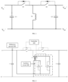
- FIG. 1 is a schematic diagram of a circuit principle of a power supply circuit of an example in some cases.
- the power supply circuit of this example is an inverting buck boost (IBB) circuit, and more specifically, may be an inverting buck boost circuit under a direct current-common (DC-C) architecture.
- IBB inverting buck boost
- DC-C direct current-common
- the power supply circuit includes: an input negative end (Vin-), an input positive end (Vin+), an output negative end (Vout-), an output positive end (Vout+), a capacitor C1, a capacitor C2, an inductor L1, a first switch module S1, and a second switch module S2.
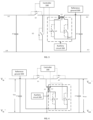
- an embodiment of the present application provides a power supply circuit.
- the power supply circuit provided by the embodiment of the present application may have a variety of circuit forms.
- FIG. 2 to FIG. 3 show several forms of the power supply circuit provided by the embodiment of the present application. It needs to be understood that the forms shown in the figures are only examples and are not intended as limitations.
- the first power supply end A1 is connected to the second power supply end A2 by means of the first switch module S1 and the first inductor L1.
- the first power supply end A1 is connected to the fourth power supply end A4 by means of the first switch module S1 and the second switch module S2.
- a first connecting end of the target module Sa1 is connected to a reference ground 300, a second connecting end of the target module Sa1 is connected to a first connecting end of the second inductor L2, a second connecting end of the second inductor L2 is connected to a first connecting end of the third switch module Sa2, and a second connecting end of the third switch module Sa2 is connected to the reference ground 300.
- the target module may be a unidirectional switch-on device, or a switch module of a signal controllable type.
- the target module may include at least one target diode, or, the target module includes a fourth switch module. It needs to be understood that the target module is shown in a form of the switch module in the accompanying drawing, which is only an example and is not intended as a limitation.
- the power supply circuit may include, but is not limited to, an inverting buck boost circuit under a direct current-common architecture, a non-isolated buck circuit under a direct current-common architecture, a non-isolated boost circuit under a direct current-common architecture, etc.
- the set position of the reference ground may vary. That is, the set position of the reference ground in the embodiment of the present application may change with the power supply circuit.
- the set position of the reference ground may be located at the first power supply end or the second power supply end.
- the reference ground is arranged at the first power supply end.
- the auxiliary circuit may further include a first diode and a second diode (not shown in FIG. 2 , referring to FIG. 5-1 hereafter).
- the second connecting end of the target module is connected to a first connecting end of the first diode, and a second connecting end of the first diode is connected to a first clamping point, where the first clamping point is arranged at the second power supply end or the third power supply end.
- the second connecting end of the second inductor is connected to a first connecting end of the second diode, and a second connecting end of the second diode is connected to a second clamping point, wherein the second clamping point is arranged at the fourth power supply end.
- the power supply circuit may be the inverting buck boost circuit.
- the first power supply end may be a power supply input negative end
- the second power supply end may be a power supply input positive end
- the third power supply end may be a power supply output negative end
- the fourth power supply end may be a power supply output positive end.
- the reference ground in the power supply circuit provided by the embodiment of the present application may not only be arranged at the first power supply end, but in another possible implementation, the reference ground may also be arranged at the second power supply end, as shown in FIG. 3 .
- the auxiliary circuit further includes a first diode and a second diode (not shown in FIG. 3 , referring to FIG. 7-1 hereafter).
- the second connecting end of the target module is connected to a first connecting end of the first diode, and a second connecting end of the first diode is connected to a first clamping point, wherein the first clamping point is arranged at the first power supply end.
- the second connecting end of the second inductor is connected to a first connecting end of the second diode, and a second connecting end of the second diode is connected to the first clamping point.
- the power supply circuit may be a non-isolated buck circuit under a direct current-common architecture.
- the first power supply end is a power supply input positive end
- the second power supply end is a power supply output positive end
- the third power supply end is a power supply output negative end
- the fourth power supply end is a power supply input negative end.
- the power supply circuit in the embodiment of the present application may not only be a non-isolated buck circuit, but may also be a non-isolated boost circuit.
- the first power supply end is a power supply output positive end
- the second power supply end is a power supply input positive end
- the third power supply end is a power supply input negative end
- the fourth power supply end is a power supply output negative end.
- FIG. 4 is a schematic diagram of a power supply circuit of an example provided by an embodiment of the present application.
- the power supply circuit in FIG. 4 may be, for example, an inverting buck boost circuit under a direct current-common architecture.
- the power supply circuit shown in FIG. 4 may include four power supply ends, a first switch module S1, a second switch module S2, and an auxiliary circuit.
- the four power supply ends may include: a power supply input negative end, a power supply input positive end, a power supply output negative end, and a power supply output positive end.
- the power supply input negative end is connected to the power supply input positive end by means of the first switch module S1 and the first inductor L1.
- the power supply input negative end is connected to the power supply output positive end by means of the first switch module S1 and the second switch module S2.
- the first switch module S1 in a first stage, the first switch module S1 is switched on, the second switch module S2 is switched off, and an input voltage Vin of a power source stores energy to the inductor L1; and in a second stage, the first switch module S1 is switched off, the second switch module S2 is switched on, and the inductor L1 releases energy through the second switch module S2, and provides the energy to a load. Conversion of the input voltage Vin to an output voltage Vout is realized by repeating the above cycle.
- a body diode of the second switch module S2 may continue the current in the inductor, and at this time, if the first switch module S1 is switched on, it will lead to a problem of a relatively heavy reverse recovery current existing in the second switch module S2.
- the embodiment of the present application introduces an auxiliary circuit 200 as in FIG. 4 .
- a part boxed in a dashed box in FIG. 4 is the introduced auxiliary circuit 200, and the auxiliary circuit includes a target module (exemplarily shown as a switch module Sa1 in the figure), a third switch module Sa2, and a second inductor L2 connected to the first inductor L1 in parallel.
- a first connecting end of the target module is connected to a reference ground 300, a second connecting end of the target module is connected to a first connecting end of the second inductor L2, a second connecting end of the second inductor L2 is connected to a first connecting end of the third switch module Sa2, and a second connecting end of the third switch module Sa2 is connected to the reference ground 300.
- the auxiliary circuit may be an auxiliary soft switching circuit.
- it may be a zero voltage turn (ZVT) circuit.
- the second inductor L2 may be a coupling inductor.
- a set position of the reference ground may be located at the power supply input negative end.
- the auxiliary circuit 200 Before the first switch module S1 is switched on, the auxiliary circuit 200 may be controlled to be switched on. At this time the inductor L2, the target module Sa1, and the third switch module Sa2 form a closed loop to control the body diode of the second switch module S2 to be switched off at a zero current without a reverse recovery loss, while the first switch module S1 may be switched on at a zero voltage.
- the power supply circuit shown in FIG. 4 may overcome the problem of high voltage spikes at two ends of the second switch module S2 in the inverting buck boost circuit to a certain extent by introducing the auxiliary circuit 200 which includes the target module Sa1, the third switch module Sa2, and the second inductor L2 connected to the first inductor in parallel, and having the first connecting end of the target module Sa1 and the second connecting end of the third switch module Sa2 in the auxiliary circuit 200 both connected to the reference ground 300.
- the auxiliary circuitry may change between switching on the third switch module Sa2 and switching off the third switch module Sa2 repeatedly in the process that the auxiliary circuit 200 realizes the soft switching function (e.g., the second switch module is switched off at the zero current, and the first switch module is switched on at the zero voltage) of the first switch module S1 and the second switch module S2.
- the third switch module Sa2 may be switched on at this time.
- impedance of the loop formed by the auxiliary circuit may be negligible, it may be regarded as a short circuit at two ends of the inductor L1, and currents in the inductor L1 all pass through the loop formed by the auxiliary circuit.
- the third switch module Sa2 may be switched off at this time.
- the embodiment of the present application introduces clamping points in the power supply circuit. This is discussed below with reference to FIG. 5-1 .
- FIG. 5-1 is a schematic diagram of a power supply circuit of another example provided by an embodiment of the present application.
- two diodes i.e., the first diode D1 and the second diode D2
- two clamping points i.e., the first clamping point and the second clamping point are added in the power supply circuit shown in FIG. 5-1 .
- the first clamping point is connected to the first diode D1
- the second clamping point is connected to the second diode D2.
- the auxiliary circuit 200 may include the first diode D1 and the second diode D2.
- the second connecting end of the target module Sa1 is connected to a first connecting end of the first diode D1, and a second connecting end of the first diode D1 is connected to the first clamping point, wherein the first clamping point is arranged at the power supply input positive end or the power supply output negative end.
- the second connecting end of the second inductor L2 is connected to a first connecting end of the second diode D2, and a second connecting end of the second diode D2 is connected to the second clamping point, wherein the second clamping point is arranged at the power supply output positive end.
- the second connecting end of the second inductor is connected to the first connecting end of the third switch module, the second connecting end of the second inductor L2 is further connected to the first connecting end of the second diode D2, and thus the first connecting end of the second diode D2 may be connected to the first connecting end of the third switch module.
- the power supply circuit shown in FIG. 5-1 uses the input negative end as the reference ground, the first connecting end of the target module is connected to the reference ground, and the second connecting end of the target module Sa1 is connected to the first clamping point by means of the first diode D1. In this way, a voltage stress of the target module in the auxiliary circuit may be clamped to the voltage between the reference ground and the first clamping point. Also, since the first clamping point may be arranged at the power supply input positive end or the power supply output negative end in FIG. 5-1 , the voltage between the reference ground and the first clamping point is Vin.
- the first connecting end of the third switch module Sa2 is connected to the second clamping point by means of the second diode D2.
- the second connecting end of the third switch module Sa2 is connected to the reference ground.
- the voltage stress of the third switch module Sa2 in the auxiliary circuit may be clamped to the voltage between the reference ground and the second clamping point.
- the second clamping point is arranged at or connected to the power supply output positive end in FIG. 5-1 , the voltage between the reference ground and the second clamping point is (Vin+Vout).
- the voltage spike stress of the target module Sa1 may be clamped to the voltage between the reference ground and the first clamping point, i.e., Vin, and energy beyond Vin is fed back to the power supply input end without loss.
- the spike voltage stress of the third switch module Sa2 may be clamped to the voltage between the reference ground and the second clamping point, i.e., (Vin+Vout), and energy beyond (Vin+Vout) is fed back to the output end.
- the voltage spike generated at the two ends of the target module Sa1 in the auxiliary circuit and the voltage spike generated between the two ends of the third switch module Sa2 in the auxiliary circuit may be reduced.
- FIG. 5-2 and FIG. 5-3 are each a schematic diagram of a power supply circuit of another example provided by an embodiment of the present application.
- FIG. 5-2 marks a clamping path of the target module Sa1 in a form of a dashed line based on FIG. 5-1 .
- FIG. 5-3 marks a clamping path of the third switch module Sa2 in a form of a dashed line based on FIG. 5-1 . That is, the clamping path of the target module Sa1 may be shown as the dashed line in FIG. 5-2 , and the clamping path of the third switch module Sa2 may be shown as the dashed line in FIG. 5-3 .
- the embodiment of the present application takes advantage of the reference ground 300 connected to the input negative end, and uses a clamping manner to reduce the voltage stresses of the target module Sa1 as well as the third switch module Sa2 without loss, which has a good application effect in an IBB topology circuit. That is, in the IBB topology circuit, independent of the limitations of input voltage and output voltage ranges, the voltage stresses on the two ends of the target module Sa1 as well as the two ends of the third switch module Sa2 in the auxiliary circuit can be effectively clamped, and a stress optimization effect is better.
- the input voltage Vin may be shocked to a very high voltage in an instant.
- the two ends of the target module Sa1 only need to withstand the Vin voltage, compared to other manners in which the spike voltage stress is much higher than the input voltage Vin, the voltage stress of the target module Sa1 in the embodiment of the present application is controlled to be within the input voltage Vin, and the reliability is high.
- the present application utilizes the input negative end as the reference ground of the target module Sa1 as well as the third switch module Sa2 to reduce the voltage stresses on the two ends of each device in the auxiliary circuit, and the manner of clamping the voltage spike stress of the target module Sa1 to be equal to the input voltage Vin enhances a voltage resistance of the soft switching circuit, and has a better lightning prevention effect in the IBB topology circuit.
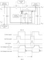
- FIG. 6 A schematic diagram of currents, voltages, and drive signals for some related devices in FIG. 5-1 and FIG. 5-2 may be shown in FIG. 6 .
- the maximum voltage between the two ends of Sa1 is clamped to Vin
- the maximum voltages between the two ends of Sa2 is clamped to (Vin+Vout).
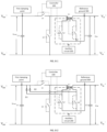
- FIG. 7-1 is a schematic diagram of a power supply circuit of an example provided by an embodiment of the present application.
- the power supply circuit in FIG. 7-1 may be, for example, a non-isolated buck circuit under a direct current-common architecture.
- the power supply circuit shown in FIG. 7-1 may include four power supply ends, a first switch module S1, a second switch module S2, and an auxiliary circuit.
- the four power supply ends may include: a power supply input negative end, a power supply input positive end, a power supply output negative end, and a power supply output positive end.
- the power supply input positive end is connected to the power supply output positive end by means of the first switch module S1 and the first inductor L1.
- the power supply input positive end is connected to the power supply output negative end by means of the first switch module S1 and the second switch module S2.
- the first switch module S1 in a first stage, the first switch module S1 is switched on, the second switch module S2 is switched off, and an input voltage Vin of a power source stores energy to the inductor L1; and in a second stage, the first switch module S1 is switched off, the second switch module S2 is switched on, and the inductor L1 releases energy through the second switch module S2 to provide the energy to a load, and conversion of the input voltage Vin to an output voltage Vout is realized by repeating the above cycle.
- the embodiment of the present application introduces an auxiliary circuit 200 in FIG. 7-1 .
- a part boxed in a dashed box in FIG. 7-1 is the introduced auxiliary circuit 200, and the auxiliary circuit includes a target module (exemplarily shown as a switch module Sa1 in the figure), a third switch module Sa2, and a second inductor L2 connected to the first inductor L1 in parallel.
- a target module exemplarily shown as a switch module Sa1 in the figure
- Sa2 exemplarily shown as a switch module Sa2 in the figure
- second inductor L2 connected to the first inductor L1 in parallel.
- the auxiliary circuit may be an auxiliary soft switching circuit.
- it may be a zero voltage turn (ZVT) circuit.
- the second inductor L2 may be a coupling inductor.
- a set position of the reference ground may be located at the power supply output positive end.
- the power supply circuit shown in FIG. 7-1 may overcome the problem of high voltage spikes at two ends of the second switch module S2 in the non-isolated buck circuit to a certain extent by introducing the auxiliary circuit 200 which includes the target module Sa1, the third switch module Sa2, and the second inductor L2 connected to the first inductor in parallel, and having the first connecting end of the target module Sa1 and the second connecting end of the third switch module Sa2 in the auxiliary circuit 200 both connected to the reference ground 300.
- the auxiliary circuitry may switch change between switching on the third switch module Sa2 and switching off the third switch module Sa2 repeatedly in the process that the auxiliary circuit 200 realizes the soft switching function (e.g., the second switch module is switched off at the zero current, and the first switch module is switched on at the zero voltage) of the first switch module S1 and the second switch module S2.
- the auxiliary circuit 200 when the auxiliary circuit 200 is configured to be switched on by the loop formed by Sa1 and Sa2, the third switch module Sa2 may be switched on at this time.
- the third switch module Sa2 If the third switch module Sa2 is switched on, impedance of the loop formed by the auxiliary circuit may be negligible, it may be regarded as a short circuit at two ends of the inductor L1, and currents in the inductor L1 all pass through the loop formed by the auxiliary circuit.
- the third switch module Sa2 may be switched off at this time.
- the third switch module Sa2 is switched off, due to the existence of a high change rate of a current on the loop of the auxiliary circuit itself (i.e., the current changes faster per unit of time), the current in the inductor L2 may pass through the target module Sa1 and the third switch module Sa2, which in turn causes the problem of reverse recovery current.
- the leakage inductance is excited by the reverse recovery current, and some devices in the auxiliary circuit may themselves generate large voltage spikes, which may reach more than twice the input voltage Vin in some cases.
- the input voltage Vin may be shocked to a very high voltage in an instant, which is prone to cause damage to the Sa1 device in the auxiliary circuit.
- higher requirements will be put forward when the Sa1 device is selected, which will undoubtedly affect a performance or increase a cost.
- the embodiment of the present application introduces clamping points in the power supply circuit. This is discussed below with reference to FIG. 7-2 .
- FIG. 7-2 is a schematic diagram of a power supply circuit of another example provided by an embodiment of the present application.
- adds two diodes i.e., the first diode D1 and the second diode D2 and a clamping point, i.e., the first clamping point are added in the power supply circuit shown in FIG. 7-1 .
- the first diode D1 and the second diode D2 are both connected to the first clamping point.
- the auxiliary circuit 200 may include the first diode D1 and the second diode D2.
- a second connecting end of the target module Sa1 is connected to a first connecting end of the first diode D1, and a second connecting end of the first diode D1 is connected to a first clamping point, wherein the first clamping point is arranged at the first power supply end.
- a second connecting end of the second inductor L2 is connected to a first connecting end of the second diode D2, and a second connecting end of the second diode D2 is connected to the first clamping point.
- the power supply circuit shown in FIG. 7-2 uses the output positive end as the reference ground, assisting a first switch tube Sa1 to be clamped to the first clamping point of the input positive end through the first diode D1, and assisting a second switch tube Sa2 to be clamped to the first clamping point of the output positive end through the second diode D2.
- the power supply circuit shown in FIG. 7-2 uses the output positive end as the reference ground, the first connecting end of the target module Sa1 is connected to the reference ground, and the second connecting end of the target module Sa1 is connected to the first clamping point by means of the first diode D1. In this way, a voltage stress of the target module Sa1 in the auxiliary circuit may be clamped to a voltage between the reference ground and the first clamping point. Also, since the first clamping point may be arranged at the power supply input positive end in FIG. 7-2 , the voltage between the reference ground and the first clamping point is (Vin-Vout).
- the first connecting end of the third switch module Sa2 is connected to the first clamping point by means of the second diode D2.
- the second connecting end of the third switch module Sa2 is connected to the reference ground.
- the voltage stress of the third switch module Sa2 in the auxiliary circuit may be clamped to a voltage between the reference ground and the first clamping point.
- the first clamping point is arranged at or connected to the power supply input positive end in FIG. 7-2 , the voltage between the reference ground and the first clamping point is (Vin-Vout).
- the voltage spike stress of the target module Sa1 may be clamped to the voltage between the reference ground and the first clamping point, i.e., (Vin-Vout), and energy beyond (Vin-Vout) is fed back to the power supply end without loss.
- the spike voltage stress of the third switch module Sa2 may be clamped to the voltage between the reference ground and the first clamping point, i.e., (Vin-Vout), and energy beyond (Vin-Vout) is fed back to the power supply end.
- FIG. 8-1 is a schematic diagram of a power supply circuit of an example provided by an embodiment of the present application.
- the power supply circuit in FIG. 8-1 may be, for example, a non-isolated boost circuit under a direct current-common architecture.
- the power supply circuit shown in FIG. 8-1 may include four power supply ends, a first switch module S1, a second switch module S2, and an auxiliary circuit.
- the four power supply ends may include: a power supply input negative end, a power supply input positive end, a power supply output negative end, and a power supply output positive end.
- the power supply output positive end is connected to the power supply input positive end by means of the first switch module S1 and the first inductor L1.
- the power supply output positive end is connected to the power supply output negative end by means of the first switch module S1 and the second switch module S2.
- the second switch module S2 in a first stage, the second switch module S2 is switched on, the first switch module S1 is switched off, and an input voltage Vin of a power source stores energy to the inductor L1; and in a second stage, the second switch module S2 is switched off, the first switch module S1 is switched on, and the inductor L1 releases energy through the first switch module S1 to provide the energy to a load, and boost conversion of the input voltage Vin to an output voltage Vout is realized by repeating the above cycle.
- the embodiment of the present application introduces an auxiliary circuit 200 in FIG. 8-1 .
- a part boxed in a dashed box in FIG. 8-1 is the introduced auxiliary circuit 200, and the auxiliary circuit includes a target module (exemplarily shown as a switch module Sa1 in the figure), a third switch module Sa2, and a second inductor L2 connected to the first inductor L1 in parallel.
- a target module exemplarily shown as a switch module Sa1 in the figure
- Sa2 exemplarily shown as a switch module Sa2 in the figure
- second inductor L2 connected to the first inductor L1 in parallel.
- the auxiliary circuit may be an auxiliary soft switching circuit.
- it may be a zero voltage turn (ZVT) circuit.
- the second inductor L2 may be a coupling inductor.
- a set position of the reference ground may be located at the power supply input positive end.
- the power supply circuit shown in FIG. 8-1 may reduce a problem of high voltage spikes at two ends of the first switch tube S1 in the non-isolated boost circuit to a certain extent by introducing the auxiliary circuit 200 which includes the target module Sa1, the third switch module Sa2, and the second inductor L2 connected to the first inductor in parallel, and having the first connecting end of the target module Sa1 and the second connecting end of the third switch module Sa2 in the auxiliary circuit 200 both connected to the reference ground 300.
- the auxiliary circuitry may change between switching on the third switch module Sa2 and switching off the third switch module Sa2 repeatedly in the process that the auxiliary circuit 200 realizes a soft switching function (e.g., the second switch module is switched off at the zero current, and the first switch module is switched on at the zero voltage) of the first switch module S1 and the second switch module S2.
- the third switch module Sa2 may be switched on at this time.
- impedance of the loop formed by the auxiliary circuit may be negligible, it may be regarded as a short circuit at two ends of the inductor L1, and currents in the inductor L1 all pass through the loop formed by the auxiliary circuit.
- the third switch module Sa2 may be switched off at this time.
- the third switch module Sa2 When the third switch module Sa2 is switched off, due to the existence of a high change rate of a current on the loop of the auxiliary circuit itself (i.e., the current changes faster per unit of time), the current in the inductor L2 may pass through the target module Sa1 and the third switch module Sa2, which in turn causes a problem of a reverse recovery current.
- the leakage inductance is excited by the reverse recovery current, and some devices in the auxiliary circuit may themselves generate large voltage spikes, which may reach more than twice the input voltage Vin in some cases.
- the input voltage Vin may be shocked to a very high voltage in an instant, which is prone to cause damage to the device in the auxiliary circuit.
- higher requirements will be put forward when the device is selected, which will undoubtedly affect a performance or increase a cost.
- the auxiliary circuit 200 may include the first diode D1 and the second diode D2.
- a second connecting end of the target module Sa1 is connected to a first connecting end of the first diode D1, and a second connecting end of the first diode D1 is connected to a first clamping point, wherein the first clamping point is arranged at the first power supply end.
- a second connecting end of the second inductor L2 is connected to a first connecting end of the second diode D2, and a second connecting end of the second diode D2 is connected to the first clamping point.
- the power supply circuit shown in FIG. 8-2 uses the input positive end as the reference ground, assisting a first switch tube Sa1 to be clamped to the first clamping point of the output positive end through the first diode D1, and assisting the second switch tube Sa2 to be clamped to the first clamping point of the output positive end through the second diode D2.
- the first connecting end of the third switch module Sa2 is connected to the first clamping point by means of the second diode D2.
- the second connecting end of the third switch module Sa2 is connected to the reference ground.
- the voltage stress of the third switch module Sa2 in the auxiliary circuit may be clamped to a voltage between the reference ground and the first clamping point.
- the first clamping point is arranged to be connected at the power supply input positive end in FIG. 8-2 , the voltage between the reference ground and the first clamping point is (Vout-Vin).
- the voltage spike stress of the target module Sa1 may be clamped to the voltage between the reference ground and the first clamping point, i.e., (Vout-Vin), and energy beyond (Vout-Vin) is fed back to the power supply end without loss.
- the spike voltage stress of the third switch module Sa2 may be clamped to the voltage between the reference ground and the first clamping point, i.e., (Vout-Vin), and energy beyond (Vout-Vin) is fed back to the power supply end.
- the individual switch module in the embodiment of the present application may be an element having a unidirectional switch-on characteristic or a signal controllable element, such as a triode, a field-effect transistor or a relay. That is, the first switch module, the second switch module, the third switch module, and the fourth switch module referred to in the embodiment of the present application may each be a triode, a field-effect transistor, or a relay.
- the field-effect transistor may be, for example, a metal-oxide-semiconductor field-effect transistor (MOSFET).
- the power supply circuit provided in the embodiment of the present application may also include a controller if needed.
- the switch modules are signal controllable elements, e.g., in a case where the first switch module is a first field-effect transistor, the second switch module is a second field-effect transistor, and the third switch module is a third field-effect transistor, gates of the first field-effect transistor, the second field-effect transistor, and the third field-effect transistor may all be connected to the controller, and switching on or off of the first field-effect transistor, the second field-effect transistor, or the third field-effect transistor is controlled by the controller. In this way, switching on and off of the individual switching modules may be conveniently controlled.
- FIG. 9 is a schematic diagram of a hardware structure of an electronic device of an embodiment of the present application.
- the electronic device 900 provided by the embodiment of the present application includes, but is not limited to, parts such as: a radio frequency unit 901, a power converter 902, an interface unit 908, a memory 909, and a processor 910.
- the power converter may be a direct current-direct current power converter. It needs to be understood that the structure of the electronic device shown in FIG. 9 does not constitute a limitation of the electronic device, and the electronic device may include more or fewer parts than illustrated, or a combination of certain parts, or a different arrangement of parts, which will not be described herein.
- the electronic device 900 provided by the embodiment of the present application may further include: a power supply circuit.
- the power supply circuit may be any of the power supply circuits provided by the above embodiments of the present application.
- the power supply circuit may include a first power supply end, a second power supply end, a third power supply end, a fourth power supply end, a first inductor, a first switch module, a second switch module, and an auxiliary circuit.
- the first power supply end is connected to the second power supply end by means of the first switch module and the first inductor.
- the first power supply end is connected to the fourth power supply end by means of the first switch module and the second switch module.
- the auxiliary circuit includes a target module, a third switch module, and a second inductor connected to the first inductor in parallel.
- a first connecting end of the target module is connected to a reference ground
- a second connecting end of the target module is connected to a first connecting end of the second inductor
- a second connecting end of the second inductor is connected to a first connecting end of the third switch module
- a second connecting end of the third switch module is connected to the reference ground.
- the power supply circuit may be located, for example, in the power converter 902. In this way, by solving the problem of a high voltage spike caused by a reverse recovery current in the power supply circuit and by introducing one or more clamping points, the electronic device may be made to operate more smoothly, thereby improving the reliability and safety.
- the electronic device provided in the embodiment of the present application may be, by way of example, a base station.
- the smooth operation of the base station may be better ensured under extreme adverse conditions (e.g., a lightning condition).
- the radio frequency unit 901 may be configured to receive and send information, e.g., for signal receiving and sending. Specifically, downlink data from a network device may be received and then given to a processor 910 for processing. Additionally, uplink data is sent to the network device.
- the radio frequency unit 901 includes, but is not limited to, an antenna, at least one amplifier, a transceiver, a coupler, a low noise amplifier, a duplexer, etc.
- the radio frequency unit 901 may further communicate with a network and other devices via a wireless communication system.
- An interface unit 908 is an interface for an external apparatus to be connected to the electronic device 900.
- the interface unit 908 may be configured to receive an input (e.g., data information, power, etc.) from an external apparatus and transmit the received input to one or more components in the electronic device 900 or may be configured to transmit data between the electronic device 900 and the external apparatus.
- an input e.g., data information, power, etc.
- the memory 909 may be configured to store various data.
- the memory 909 may include a highspeed random access memory, and may further include a non-volatile memory, etc.
- the processor 910 is the control center of the electronic device, connects various portions of the entire electronic device using various interfaces and lines, and performs various functions and processes data of the electronic device by operating or executing software programs and/or modules stored in the memory 909 and by calling data stored in the memory 909, so as to monitor the electronic device as a whole.
- the processor 910 may include one or more processing units.
- the electronic device 900 includes some functional modules that are not shown, which will not be repeated herein.
- the power converter 902 may include a controller (e.g. corresponding to the processor 910) as well as a power conversion circuit.
- the power conversion circuit is configured to convert input power provided to the power converter by an input power source to output power of a load, the input power source may be an additional power source connected to the power converter, and the load may be an output load connected to the power converter.
- FIG. 10-1 is a schematic diagram of a communication system provided by an embodiment of the present application.
- the communication system 1000 provided by the embodiment of the present application may include: an electronic device 1010 and a load 1020.
- the electronic device is connected to the load.
- a structure of the electronic device 1010 may refer to FIG. 9 .
- the electronic device may include a power converter, and the power converter may be configured to supply power to the load.
- the power converter may be a direct current-direct current converter (DC-DC converter).
- the communication system provided by the embodiment of the present application may further include an alternating current-direct current converter 1005, and the alternating current-direct current converter 1005 is connected to the direct current-direct current converter 1011.
- the load includes a remote radio unit 1021.
- the direct current-direct current converter 1011 is connected to the remote radio unit.
- a current output from a power grid may first pass through an alternating current-direct current (AC-DC) converter 1005 to convert the alternating current output from the power grid to a direct current.
- the current then passes through a direct current-direct current (DC-DC) converter 1011 (corresponding to the power converter 902 in FIG. 9 ) to distribute power for a power amplifier of the remote radio unit 1021. That is, power distribution may be performed using the DC-DC converter (a power converter) in a communication direct current power supply system.
- AC-DC alternating current-direct current
- DC-DC direct current-direct current
- the communication system provided by the embodiment of the present application may make the communication system operate more smoothly and improve reliability and safety by solving a problem of a high voltage spike caused by a reverse recovery current in the power supply circuit, and by introducing one or more clamping points.
Landscapes
- Engineering & Computer Science (AREA)
- Power Engineering (AREA)
- Theoretical Computer Science (AREA)
- Physics & Mathematics (AREA)
- General Engineering & Computer Science (AREA)
- General Physics & Mathematics (AREA)
- Dc-Dc Converters (AREA)
Applications Claiming Priority (2)
| Application Number | Priority Date | Filing Date | Title |
|---|---|---|---|
| CN202211066864.4A CN117674568A (zh) | 2022-09-01 | 2022-09-01 | 供电电路、电子设备及通信系统 |
| PCT/CN2023/115451 WO2024046302A1 (zh) | 2022-09-01 | 2023-08-29 | 供电电路、电子设备及通信系统 |
Publications (2)
| Publication Number | Publication Date |
|---|---|
| EP4576535A1 true EP4576535A1 (de) | 2025-06-25 |
| EP4576535A4 EP4576535A4 (de) | 2025-11-19 |
Family
ID=90079551
Family Applications (1)
| Application Number | Title | Priority Date | Filing Date |
|---|---|---|---|
| EP23859332.1A Pending EP4576535A4 (de) | 2022-09-01 | 2023-08-29 | Stromversorgungsschaltung, elektronische vorrichtung und kommunikationssystem |
Country Status (4)
| Country | Link |
|---|---|
| EP (1) | EP4576535A4 (de) |
| KR (1) | KR20250039476A (de) |
| CN (1) | CN117674568A (de) |
| WO (1) | WO2024046302A1 (de) |
Families Citing this family (1)
| Publication number | Priority date | Publication date | Assignee | Title |
|---|---|---|---|---|
| CN118449260B (zh) * | 2024-07-08 | 2024-08-30 | 中通服网盈科技有限公司 | 一种5g基站发电油机智能运行系统 |
Family Cites Families (8)
| Publication number | Priority date | Publication date | Assignee | Title |
|---|---|---|---|---|
| US5977754A (en) * | 1999-02-01 | 1999-11-02 | Astec International Limited | Offset resonance zero volt switching boost converter |
| US6188209B1 (en) * | 2000-02-07 | 2001-02-13 | University Of Hong Kong | Stepping inductor for fast transient response of switching converter |
| US6815937B2 (en) * | 2002-10-24 | 2004-11-09 | The University Of Hong Kong | Stepping inductor for fast transient response of switching converter |
| US8115460B2 (en) * | 2010-01-23 | 2012-02-14 | Moshe Kalechshtein | Power conversion with zero voltage switching |
| CN105119489B (zh) * | 2015-08-28 | 2017-10-31 | 株洲南车时代电气股份有限公司 | 一种双向升降压斩波电路 |
| CN108900083B (zh) * | 2018-06-05 | 2020-09-18 | 华为技术有限公司 | 功率转换器及相关系统 |
| IT201900006719A1 (it) * | 2019-05-10 | 2020-11-10 | St Microelectronics Srl | Convertitore elettronico |
| CN115039328A (zh) * | 2020-05-29 | 2022-09-09 | 华为数字能源技术有限公司 | 一种开关电感功率变换器、通信系统及方法 |
-
2022
- 2022-09-01 CN CN202211066864.4A patent/CN117674568A/zh active Pending
-
2023
- 2023-08-29 KR KR1020257006371A patent/KR20250039476A/ko active Pending
- 2023-08-29 EP EP23859332.1A patent/EP4576535A4/de active Pending
- 2023-08-29 WO PCT/CN2023/115451 patent/WO2024046302A1/zh not_active Ceased
Also Published As
| Publication number | Publication date |
|---|---|
| EP4576535A4 (de) | 2025-11-19 |
| KR20250039476A (ko) | 2025-03-20 |
| CN117674568A (zh) | 2024-03-08 |
| WO2024046302A1 (zh) | 2024-03-07 |
Similar Documents
| Publication | Publication Date | Title |
|---|---|---|
| US12169428B2 (en) | Power supply apparatus, power supply system, and data center | |
| US11784552B2 (en) | Power converter and related system | |
| US8270129B2 (en) | Device arranged for converting an AC input voltage to a DC output voltage | |
| EP2911282A1 (de) | Stromquelle und spannungsregelverfahren für die stromquelle | |
| JP6189786B2 (ja) | 電源装置、及び電源装置の制御方法 | |
| CN105657900A (zh) | 调光电路、控制电路和调光方法 | |
| EP4148932B1 (de) | Stromversorgungsvorrichtung und stromversorgungsverfahren | |
| US20240055985A1 (en) | Active Current Limiting Circuit, Power Supply Device, Power Supply System and Control Method | |
| CN102315759B (zh) | 具有抗饱和电路的栅极驱动控制器电路及其加电电路 | |
| US20230036842A1 (en) | Dc-to-dc converter with freewheeling circuits | |
| EP4576535A1 (de) | Stromversorgungsschaltung, elektronische vorrichtung und kommunikationssystem | |
| US11277036B2 (en) | Rectenna controller and rectenna apparatus including the same | |
| EP4589830A1 (de) | Gleichstromwandlerschaltung und photovoltaikwechselrichter | |
| US20240055855A1 (en) | Active current limiting circuit, power supply device, power supply system and control method | |
| US9582016B2 (en) | Boost converter with capacitive boost stages | |
| US20220385187A1 (en) | Switch-mode power supply | |
| US20110286245A1 (en) | Dc/dc power converter having active self driving synchronous rectification | |
| WO2021017697A1 (zh) | 一种局端设备、供电系统、触电保护方法及装置 | |
| CN106787628B (zh) | 变换器互联系统的控制方法及变换器的控制电路 | |
| CN210958156U (zh) | 一种双向直流变换电路 | |
| US20250047200A1 (en) | Single inductor multiple output regulator | |
| CN107483009A (zh) | 一种光伏发电系统的优化器旁路控制方法 | |
| US20230137732A1 (en) | Power Conversion System, Power Conversion Module, and Processing Apparatus | |
| US10439487B2 (en) | Voltage converter circuit and method for operating a voltage converter circuit | |
| CN119362885A (zh) | 一种优化器、优化器的控制方法和光伏发电系统 |
Legal Events
| Date | Code | Title | Description |
|---|---|---|---|
| STAA | Information on the status of an ep patent application or granted ep patent |
Free format text: STATUS: THE INTERNATIONAL PUBLICATION HAS BEEN MADE |
|
| PUAI | Public reference made under article 153(3) epc to a published international application that has entered the european phase |
Free format text: ORIGINAL CODE: 0009012 |
|
| STAA | Information on the status of an ep patent application or granted ep patent |
Free format text: STATUS: REQUEST FOR EXAMINATION WAS MADE |
|
| 17P | Request for examination filed |
Effective date: 20250318 |
|
| AK | Designated contracting states |
Kind code of ref document: A1 Designated state(s): AL AT BE BG CH CY CZ DE DK EE ES FI FR GB GR HR HU IE IS IT LI LT LU LV MC ME MK MT NL NO PL PT RO RS SE SI SK SM TR |
|
| A4 | Supplementary search report drawn up and despatched |
Effective date: 20251021 |
|
| RIC1 | Information provided on ipc code assigned before grant |
Ipc: H02M 1/32 20070101AFI20251015BHEP Ipc: H02M 3/158 20060101ALI20251015BHEP Ipc: G06F 1/26 20060101ALI20251015BHEP Ipc: H02M 1/00 20060101ALI20251015BHEP Ipc: H02M 1/088 20060101ALI20251015BHEP Ipc: H03K 17/081 20060101ALI20251015BHEP |
|
| DAV | Request for validation of the european patent (deleted) | ||
| DAX | Request for extension of the european patent (deleted) |