EP4576216A1 - Dispositif de protection contre les décharges électrostatiques en tranchée - Google Patents
Dispositif de protection contre les décharges électrostatiques en tranchée Download PDFInfo
- Publication number
- EP4576216A1 EP4576216A1 EP23219323.5A EP23219323A EP4576216A1 EP 4576216 A1 EP4576216 A1 EP 4576216A1 EP 23219323 A EP23219323 A EP 23219323A EP 4576216 A1 EP4576216 A1 EP 4576216A1
- Authority
- EP
- European Patent Office
- Prior art keywords
- trenches
- trench
- doped regions
- semiconductor device
- metal layer
- Prior art date
- Legal status (The legal status is an assumption and is not a legal conclusion. Google has not performed a legal analysis and makes no representation as to the accuracy of the status listed.)
- Pending
Links
Images


Classifications
-
- H—ELECTRICITY
- H10—SEMICONDUCTOR DEVICES; ELECTRIC SOLID-STATE DEVICES NOT OTHERWISE PROVIDED FOR
- H10D—INORGANIC ELECTRIC SEMICONDUCTOR DEVICES
- H10D89/00—Aspects of integrated devices not covered by groups H10D84/00 - H10D88/00
- H10D89/60—Integrated devices comprising arrangements for electrical or thermal protection, e.g. protection circuits against electrostatic discharge [ESD]
- H10D89/601—Integrated devices comprising arrangements for electrical or thermal protection, e.g. protection circuits against electrostatic discharge [ESD] for devices having insulated gate electrodes, e.g. for IGFETs or IGBTs
- H10D89/611—Integrated devices comprising arrangements for electrical or thermal protection, e.g. protection circuits against electrostatic discharge [ESD] for devices having insulated gate electrodes, e.g. for IGFETs or IGBTs using diodes as protective elements
-
- H—ELECTRICITY
- H02—GENERATION; CONVERSION OR DISTRIBUTION OF ELECTRIC POWER
- H02H—EMERGENCY PROTECTIVE CIRCUIT ARRANGEMENTS
- H02H9/00—Emergency protective circuit arrangements for limiting excess current or voltage without disconnection
- H02H9/04—Emergency protective circuit arrangements for limiting excess current or voltage without disconnection responsive to excess voltage
- H02H9/045—Emergency protective circuit arrangements for limiting excess current or voltage without disconnection responsive to excess voltage adapted to a particular application and not provided for elsewhere
- H02H9/046—Emergency protective circuit arrangements for limiting excess current or voltage without disconnection responsive to excess voltage adapted to a particular application and not provided for elsewhere responsive to excess voltage appearing at terminals of integrated circuits
-
- H—ELECTRICITY
- H10—SEMICONDUCTOR DEVICES; ELECTRIC SOLID-STATE DEVICES NOT OTHERWISE PROVIDED FOR
- H10D—INORGANIC ELECTRIC SEMICONDUCTOR DEVICES
- H10D30/00—Field-effect transistors [FET]
- H10D30/60—Insulated-gate field-effect transistors [IGFET]
- H10D30/64—Double-diffused metal-oxide semiconductor [DMOS] FETs
- H10D30/66—Vertical DMOS [VDMOS] FETs
- H10D30/668—Vertical DMOS [VDMOS] FETs having trench gate electrodes, e.g. UMOS transistors
-
- H—ELECTRICITY
- H10—SEMICONDUCTOR DEVICES; ELECTRIC SOLID-STATE DEVICES NOT OTHERWISE PROVIDED FOR
- H10D—INORGANIC ELECTRIC SEMICONDUCTOR DEVICES
- H10D84/00—Integrated devices formed in or on semiconductor substrates that comprise only semiconducting layers, e.g. on Si wafers or on GaAs-on-Si wafers
- H10D84/101—Integrated devices comprising main components and built-in components, e.g. IGBT having built-in freewheel diode
- H10D84/141—VDMOS having built-in components
- H10D84/148—VDMOS having built-in components the built-in components being breakdown diodes, e.g. Zener diodes
-
- H—ELECTRICITY
- H10—SEMICONDUCTOR DEVICES; ELECTRIC SOLID-STATE DEVICES NOT OTHERWISE PROVIDED FOR
- H10D—INORGANIC ELECTRIC SEMICONDUCTOR DEVICES
- H10D84/00—Integrated devices formed in or on semiconductor substrates that comprise only semiconducting layers, e.g. on Si wafers or on GaAs-on-Si wafers
- H10D84/101—Integrated devices comprising main components and built-in components, e.g. IGBT having built-in freewheel diode
- H10D84/141—VDMOS having built-in components
- H10D84/143—VDMOS having built-in components the built-in components being PN junction diodes
Definitions
- the present disclosure relates to a semiconductor device and in particular to a semiconductor device comprising electrostatic protection devices formed in trenches of a semiconductor device.
- Electrostatic discharge is the sudden transfer of charge between differently charged objects.
- Certain electrical components formed as part of semiconductor devices e.g. MOS based transistor devices
- MOS based transistor devices are at risk of being damaged by ESD. This is particularly likely to be the case where the gate oxide layer of the transistor device is thinned to provide a lower threshold voltage for operation.
- ESD protection devices may be used to protect against sudden ESD events, in order to prevent active components, e.g. transistors from suffering damage.
- Such ESD protection devices may comprise one or more diodes connected to an active electrical component. At least some of these diodes are arranged such that in the event of ESD, the current flows in the reverse direction through the diode, and hence the diodes only conduct current in the event of a sudden large voltage spike.
- a type of electrical component that may require the implementation of ESD protection devices is a trench gate transistor device.
- Trench gate transistor devices are formed in trenches provided in a semiconductor substrate.
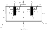
- Figure 1 illustrates a semiconductor device 100 in which trench gate transistor devices are formed.
- the semiconductor device 100 comprises a substrate 102, a lower part 108 of the substrate 102 is an N doped region 108, whilst an upper part 106 of the substrate is a P doped region 106.
- the semiconductor device 100 further comprises trenches 104 formed in the substrate 102.
- Gate electrodes 112 are formed within the trenches 104 in the substrate 102 and insulating material 114 is formed on the sides of the trenches 104.
- a drain metal electrode 118 is formed on the lower side of the semiconductor substrate 102, whilst a source electrode 116 is formed on the upper side of the semiconductor substrate 102.
- the transistor device When a positive voltage is applied to the gate electrodes 112, the transistor device is turned on and a current may flow vertically between the source electrode 116 and the drain electrode 118.
- One approach to providing ESD protection devices is to form a polysilicon layer above the semiconductor substrate and to form a plurality of P doped and N doped regions in the polysilicon layer, such that pairs of the P doped and N doped regions form PN junctions, hence providing diodes for providing ESD protection.
- an additional photomask may be required in order to define the polysilicon layer pattern, resulting in a more expensive manufacturing process.
- each well comprises a PN junction and/or an NP junction.
- the formation of these wells may eliminate the need for a further polysilicon layer formed above the substrate.
- the process required to produce such wells differs from the processes normally used to produce the trenches in active regions, e.g. the trenches in which the gates of transistors are formed.
- the formation of such different trench geometries increases the complexity and cost associated with fabricating the semiconductor device.
- surface area utilisation associated with the use of such wells may be sub-optimal.
- a semiconductor device comprising: a semiconductor substrate comprising a plurality of trenches arranged in parallel, each of the trenches comprising a semiconductor comprising a plurality of first doped regions and a second doped region; a plurality of trench electrostatic discharge protection devices formed in the trenches and connected between a first metal layer formed above the semiconductor substrate and a second metal layer formed above the semiconductor substrate, wherein each of the plurality of trenches comprises two or more of the trench electrostatic discharge protection devices, wherein each of the plurality of trench electrostatic discharge protection devices comprises at least one of a PN junction or NP junction formed between one of the first doped regions and the second doped region of the respective trench, wherein the semiconductor device further comprising a plurality of connection electrodes formed above the semiconductor substrate for connecting the electrostatic discharge protection devices of each trench to the electrostatic protection devices of an adjacent at least one of the trenches, wherein for a first outer one of the trenches, the electrostatic discharge protection devices of the first outer one
- Each of the trenches comprises a plurality of ESD protection devices formed by PN or NP junctions between respective first doped regions (e.g. a P-doped region) and a second doped region (e.g. an N-doped region).
- the ESD protection devices are connected in series across the trenches by connection electrodes, which connect the trenches at corresponding points.
- the two outer trenches comprise ESD protection devices that are connected in parallel to first and second metal layers.
- the first and second metals between which the ESD protection devices are connected may, for example, be source and gate metal layers. An ESD event causes current to flow through the ESD protection devices.
- the ESD protection devices are connected in parallel between a first metal layer, which may be connected to source electrodes of the transistors, and a second metal layer, which may be connected to gate electrodes of the transistors.
- the ESD protection devices are formed in parallel across trenches, enabling greater surface area utilisation and better integration with the techniques for forming trenches in a neighbouring active region.
- the use of the stripped arrangement of trenches make it possible to design a network ESD protection devices to achieve the appropriate current carrying capacity and breakdown voltage.
- a first region is an active region in which the trench gate transistors using first trenches are formed.
- the second region comprises the trenches (i.e. the second trenches) in which ESD protection devices are formed.
- the second trenches are arranged in parallel with the first trenches and used for the formation of the ESD protection devices.
- connection electrodes are configured to, for each of the electrostatic protection devices: provide a connection between a terminal of the respective electrostatic protection device and a terminal of a corresponding electrostatic protection device in the adjacent at least one of the trenches; and/or provide a connection between a terminal of the respective electrostatic protection device and terminals of a plurality of electrostatic protection devices in the adjacent at least one of the trenches.
- the electrostatic protection devices may be said to be corresponding if they are located in an equivalent position within different trenches.
- each of the connection electrodes form connections between: corresponding ones of the first doped regions belonging to different trenches; or the second doped regions belonging to different trenches.
- the first doped regions may be said to be corresponding if they are located in an equivalent position within different trenches.
- the semiconductor device further comprises: an insulating layer over the plurality of trenches; and conductive contacts formed through the insulating layer and connected to the connection electrodes.
- At least some of the conductive contacts are in contact with ones of the first doped regions of the trenches.
- some of the conductive contacts are in contact with ones of the second doped regions of the trenches.
- the plurality of trenches are a plurality of second trenches disposed in a second region of the semiconductor substrate, wherein the semiconductor device further comprises at least one first trench disposed in a first region defined in the semiconductor substrate, wherein one or more trench gate transistor devices are disposed in the first device region, the one or more trench gate transistor devices comprising gates disposed in the at least one first trench.
- the first metal layer is electrically connected to a first terminal of each of the trench gate transistor devices, wherein the second metal layer is electrically connected to a second terminal of each of the trench gate transistor devices.
- the second trenches are deeper than the at least one first trench.
- connections electrodes form connections with the second doped regions belonging to different trenches.
- each of the trenches comprises third doped regions electrically connected to ones of the connection electrodes connected to the respective trench, wherein each of the third doped regions comprises a same doping type as the first doped regions, wherein the third doped regions are more heavily doped that the first doped regions.
- the first metal layer is a source metal layer connected to a source terminal of a transistor of the semiconductor device.
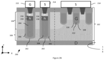
- the semiconductor device 100 comprises a substrate 102, which may be formed of silicon.
- the semiconductor device comprises a first region 210 of the substrate 102, which is an active region 210 in which the trench gate transistors are formed.
- the trenches 104 for forming the gates of the transistors are shown as formed within this first region 210.
- the transistors formed within this region 210 may be the same as those shown in Figure 1 .
- a drain metal layer 118 On the rear side of the substrate 102 is shown a drain metal layer 118, which provides the drain terminal of the transistors.
- the semiconductor device 200 in addition to the active region 210, also comprises a second region 212 of the substrate 102.
- the second region 212 comprises the ESD protection devices, which are also formed in trenches.
- the second region 212 comprises the ESD protection devices, which are also formed in trenches 202.
- the trenches 202 may be formed with the same trench geometry, e.g. the same width, depth, and length as the trenches 104 of the first region 210.
- an insulating material 206 which separates a semiconductor material 204 formed in the trenches from the material of the semiconductor substrate 102.
- the semiconductor material 204 may be polysilicon 204.
- the semiconductor material 204 formed in the trenches comprises first doped regions 216 and second doped regions 218.
- the first doped regions 216 are P-doped regions, whilst the second doped regions 218 are N-doped regions.
- the P-doping and N-doping regions may reversed, i.e. the first doped regions 216, described in the examples as being P-doped, may be N-doped, whilst the second doped regions 218, described in the examples as being N-doped, may be P-doped.
- conductive contacts 220 are in electrical contact with the P-doped regions 216 of the trenches 202. Some of these contacts 220 are in electrical contact with a metal layer 222 (which is a gate metal layer 222 in the example of Figure 2A ), forming electrical connections between the gate metal layer 222 and the respective P-doped regions 216. Some of the contacts 220 are in electrical contact with the metal layer 214 (which is a source metal layer 214 in the example of Figure 2A ) forming electrical connections between the source metal layer 214 and the respective P-doped regions 216.
- a metal layer 222 which is a gate metal layer 222 in the example of Figure 2A
- the contacts 220 are in electrical contact with the metal layer 214 (which is a source metal layer 214 in the example of Figure 2A ) forming electrical connections between the source metal layer 214 and the respective P-doped regions 216.
- the metal layers 214, 222 are shown in the example of Figure 2A as being source metal layers 214 and gate metal layer 222, the metal layers 214, 222 may be connected to other components than the source and gate terminal of a transistor.
- one of the metal layers 214, 222 may be a drain metal layer for connection to the drain electrode 118 of the transistor, whilst another of the metal layers 214, 222 may be a gate metal layer. Therefore, the metal layer 214 is described herein as being a first metal layer 214, whilst the metal layer 222 is described herein as being a second metal layer 222.
- contacts 220 shown in Figure 2A may be formed to form connections between P-doped region or N-doped regions of different trenches 202 so as to form series connections between ESD protection devices implemented in different trenches 202. These connections are described in more detail with respect to Figures 4A and 4B .
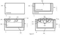
- FIG. 2B illustrates a further example embodiment of the semiconductor device in which the trenches 202 for forming the ESD protection devices are larger than the trenches 104.
- the smaller size trench ranges from 0.6.
- the trenches 202 in this embodiment are deep trench isolation (DTI) trenches.
- the deep isolation trenches may provide a higher breakdown voltage for the resulting ESD protection devices.
- the smaller sized trenches 202 shown in Figure 2A may be between 0.6 ⁇ m and 1.8 ⁇ m in depth.
- the deep sized trenches 202 shown in Figure 2B may be between 2 ⁇ m and 12 ⁇ m in depth.
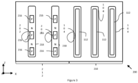
- FIG. 3 illustrates a top-view of the semiconductor device 200.
- both sets of trenches 104 and 202 extend across the device 200 in a further direction (i.e. the Z-direction) that is perpendicular to the vertical direction (i.e. the Y-direction) in which the trenches are formed in the substrate 102.
- the trenches 104, 202 are arranged parallel to one another.
- the gate electrodes 114 are shown formed in the trenches 104.
- each of the trenches 202 comprises a plurality of P-doped regions 216, which are separated from one another by an N-doped region 218.
- the semiconductor device 100 comprises four trenches 202a-d.
- the number of trenches 202 may be a different number that is greater than or equal to two.
- the number of first doped-regions 216 is shown as being equal to three, but could be a different number.
- Figure 4A is a top view showing the trenches 202a-d and the conductive structures above the trenches 202.
- the conductive structures may be made of copper. These conductive structures include the source metal layer 220 and the second metal layer 222 discussed with respect to Figures 2A and 2B .
- the source metal layer 220 is connected to the P-doped regions 216 of a first outer trench 202a, whilst the second metal layer 222 is connected to the P-doped regions 216 of a second outer trench 202d.
- the conductive structures also include connection electrodes 402 for forming connections between adjacent ones of the trenches 402a-d.
- connection electrodes 402 may also be referred to as connection structures 402 and form a further metal layer for forming connections between the trenches 202a-d.
- Each of the trenches 202a-d is connected to its adjacent trenches (of which there are either one or two) via the connection electrodes 402.
- the connection electrodes 402 are at a floating potential.
- the semiconductor device 200 comprises three contacts 220 implemented in the insulating layer 110 that connect respective P-doped regions 216 of the trench 202a to respective parts of the first metal layer 214.
- a second trench 202b located adjacent to the first trench 202a is electrically connected at a number of points to the first trench 202a.
- a plurality of contacts 400 are formed through the insulating layer 110 for connecting the N-doped regions 218 of the first and second trenches 202a, 202b to connection electrodes 402.
- the connection electrodes 402 are parts of a further metal layer for forming connections between the trenches 202a-d.
- the device 200 comprises three contacts 400 forming electrical connections between the N-doped region 218 of the trench 202a and the connecting structures 402 and three contacts 400 forming electrical connections between the N-doped region 218 of the trench 202b and the same connecting structures 402. Hence, at these three points, the N-doped regions 218 of the trenches 202a, 202b are electrically connected.
- a third trench 202c is located adjacent to the second trench 202b and is electrically connected to the second trench 202b.
- the connections are formed between respective P-doped regions 216 of the two trenches 202b, 202c.
- Contacts formed through the insulating layer 110 connect the P-doped regions of the trenches 202b, 202c to respective connecting structures 400.
- an electrical connection is formed between respective P-doped regions of the trenches 202b, 202c via the contacts 400 and the connecting structures 402.
- a fourth trench 202d is located adjacent to the third trench 202c and is located at an edge of the set of trenches that is opposite to the edge at which the first trench 202a is located.
- a plurality of contacts 400 are formed through the insulating layer 110 for connecting the N-doped regions 218 of the third and fourth trenches 202a, 202b to connection electrodes 402, so as to electrically connect the N-doped regions of the third and fourth trenches 202c, 202d.
- a plurality of contacts 220 are formed in contact with the P-doped regions 216 of the fourth trench 202d. These contacts 220 are connected to the second metal layer 222.
- Each parallel connection comprises a number of ESD protection devices arranged in series for providing a high breakdown voltage, such that current flows only in response to a large potential difference, e.g. resulting from an ESD event.
- FIG. 4B illustrates a further view of a trench 202 and its corresponding contacts 220/400, 400.
- the trench 202 may be any of the trenches 202a-d shown in Figure 4A . However, if the trench 202 is one of the outer trenches 202a,d, the contacts labelled as 220/400 are contacts 220. On the other hand, if the trench 202 is one of the inner trenches 202b,c, the contacts 220/400 are contacts 400.
- ESD protection devices 404j,k,l comprise PN junctions formed in trench 202d. As a result, the ESD protection devices 404j,k,l are connected in parallel with one another between the second metal layer 222 and the N-doped region 218 of trench 202d.
- the ESD protection devices 404a-I provide protection against ESD events by allowing current to flow through the circuit 500 formed by these device 404a-I when a large potential difference exists between the first metal layer 214 and the second metal layer 222. Since the devices 404a-I comprise multiple diodes 404a-I implemented with different polarity, a large potential difference is required to cause current to flow (either from layer 214 to layer 222 or from layer 222 to layer 214) in the reverse direction through some of the diodes. The number of diodes 404a-I connected together in series can be increased to increase the breakdown voltage at which current flows between metal layers 214 and 222 through the circuit 500.
- the number of diodes 404a-I may be increased either by adding further trenches 202 to the set of trenches 202 or by adding additional P-doped regions connected to the connection electrodes 400 (as described below with reference to Figure 6 ).
- the total current carrying capacity of the circuit 500 may be increased by adding additional ESD devices connected in parallel.
- the example circuit 500 has sets of three ESD devices that are connected in parallel. However, by adding additional P-doped regions and connection electrodes, this number may be increased.
- the second trench 202b comprises a third set 600c of ESD protection devices 202 arranged in parallel and formed by the PN junctions between P-doped regions 216 and the N-doped region 218 of that trench 202b.
- associated pairs of ESD protection devices belonging to the second set 600b and the third set 600c are arranged in series with one another, since they are connected by respective one of the connection electrodes 402.
- the second trench 202b further comprises a fourth set 600d of ESD protection devices arranged in parallel and formed by the NP junctions between the N-doped region 218 of that trench 202b and the P-doped regions of that trench 202b.
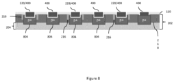
- the second doped-region 218 of the trench 202 is implanted.
- a contact mask is then used to define the first-doped regions 216 and the first-doped regions are implanted.
- the electrically insulating layer 110 is then formed on the surface of the substrate 102.
- the contacts 900 are etched through the insulating layer 110 to form connections through the insulating layer 110 with the first-doped regions 216 and the second doped region 218.
- Each of the contacts 900 is one of the contacts 220/400 discussed earlier.
- the metal layers 902 are then deposited on each of the contacts.
- Each of the metal layers 902 is a connection electrode 402 or is part of the first metal layer 214 or second metal layer 222.
- Figure 9 illustrates the process for constructing one trench 202, but a similar process may be followed for constructing other similar trenches 202.
- the metal layers 902 are formed on different trenches 202 to connect the trenches 202, between the first metal layer 214 and second metal layer 222, e.g. as discussed with respect to Figures 4A , 5 or 7 .
- a similar process to that illustrated in Figure 9 may be applied to produce the example trenches 202 shown in Figures 6 and 8 .
- the process may be the same, but with additional first doped region implants 216a added at stage 3.
- the process may be the same, but with heavily doped region implants 804 added at Figure 8 .
Landscapes
- Engineering & Computer Science (AREA)
- Microelectronics & Electronic Packaging (AREA)
- Metal-Oxide And Bipolar Metal-Oxide Semiconductor Integrated Circuits (AREA)
- Semiconductor Integrated Circuits (AREA)
Priority Applications (3)
| Application Number | Priority Date | Filing Date | Title |
|---|---|---|---|
| EP23219323.5A EP4576216A1 (fr) | 2023-12-21 | 2023-12-21 | Dispositif de protection contre les décharges électrostatiques en tranchée |
| CN202411867069.4A CN120201785A (zh) | 2023-12-21 | 2024-12-18 | 沟槽静电放电保护器件 |
| US18/987,917 US20250212526A1 (en) | 2023-12-21 | 2024-12-19 | Trench electrostatic discharge protection device |
Applications Claiming Priority (1)
| Application Number | Priority Date | Filing Date | Title |
|---|---|---|---|
| EP23219323.5A EP4576216A1 (fr) | 2023-12-21 | 2023-12-21 | Dispositif de protection contre les décharges électrostatiques en tranchée |
Publications (1)
| Publication Number | Publication Date |
|---|---|
| EP4576216A1 true EP4576216A1 (fr) | 2025-06-25 |
Family
ID=89308416
Family Applications (1)
| Application Number | Title | Priority Date | Filing Date |
|---|---|---|---|
| EP23219323.5A Pending EP4576216A1 (fr) | 2023-12-21 | 2023-12-21 | Dispositif de protection contre les décharges électrostatiques en tranchée |
Country Status (3)
| Country | Link |
|---|---|
| US (1) | US20250212526A1 (fr) |
| EP (1) | EP4576216A1 (fr) |
| CN (1) | CN120201785A (fr) |
Citations (3)
| Publication number | Priority date | Publication date | Assignee | Title |
|---|---|---|---|---|
| US20100258853A1 (en) * | 2009-04-10 | 2010-10-14 | Wei-Chieh Lin | Trench semiconductor device and method of making the same |
| US20150349091A1 (en) * | 2014-05-31 | 2015-12-03 | Hamza Yilmaz | Semiconductor power devices manufactured with self-aligned processes and more reliable electrical contacts |
| US20230134063A1 (en) * | 2021-10-29 | 2023-05-04 | Stmicroelectronics (Rousset) Sas | Electronic device comprising transistors |
-
2023
- 2023-12-21 EP EP23219323.5A patent/EP4576216A1/fr active Pending
-
2024
- 2024-12-18 CN CN202411867069.4A patent/CN120201785A/zh active Pending
- 2024-12-19 US US18/987,917 patent/US20250212526A1/en active Pending
Patent Citations (3)
| Publication number | Priority date | Publication date | Assignee | Title |
|---|---|---|---|---|
| US20100258853A1 (en) * | 2009-04-10 | 2010-10-14 | Wei-Chieh Lin | Trench semiconductor device and method of making the same |
| US20150349091A1 (en) * | 2014-05-31 | 2015-12-03 | Hamza Yilmaz | Semiconductor power devices manufactured with self-aligned processes and more reliable electrical contacts |
| US20230134063A1 (en) * | 2021-10-29 | 2023-05-04 | Stmicroelectronics (Rousset) Sas | Electronic device comprising transistors |
Also Published As
| Publication number | Publication date |
|---|---|
| US20250212526A1 (en) | 2025-06-26 |
| CN120201785A (zh) | 2025-06-24 |
Similar Documents
| Publication | Publication Date | Title |
|---|---|---|
| EP2985790B1 (fr) | Dispositif à semi-conducteur et procédé de fabrication de dispositif à semi-conducteur | |
| US7952137B2 (en) | Trench semiconductor device and method of making the same | |
| KR101464885B1 (ko) | 정전기 방전 보호를 위한 장치 | |
| TWI430432B (zh) | 具有防靜電結構之功率半導體元件及其製作方法 | |
| US9741846B2 (en) | Semiconductor device | |
| CN113540073A (zh) | 包括垂直沟道结构的集成电路和该集成电路的布局方法 | |
| US11652167B2 (en) | Semiconductor device having junction termination structure and method of formation | |
| TW201535719A (zh) | 帶有自對準接觸增強型插頭之高密度溝槽閘極mosfet陣列及其製備方法 | |
| CN112951823B (zh) | 半导体器件 | |
| US10784251B2 (en) | Internally stacked NPN with segmented collector | |
| DE102023102551A1 (de) | Halbleitervorrichtung und herstellungsverfahren | |
| CN112534569A (zh) | 半导体装置、功率模块以及半导体装置的制造方法 | |
| CN113782527A (zh) | 静电放电器件和包括该静电放电器件的静电放电保护电路 | |
| EP4576216A1 (fr) | Dispositif de protection contre les décharges électrostatiques en tranchée | |
| US10249614B2 (en) | Semiconductor device | |
| JP4326762B2 (ja) | 横型トレンチ構造を有するショットキー・バリア・ダイオード及びその製造方法 | |
| US5831312A (en) | Electrostic discharge protection device comprising a plurality of trenches | |
| US10680087B2 (en) | Gated diode having fingers with elevated gates | |
| CN118073408A (zh) | 半导体结构及其形成方法 | |
| CN110678979B (zh) | 用于沟槽dmos的沟槽内集成堆叠esd网络 | |
| CN118486738B (zh) | 提高静电能力的功率半导体器件及制造方法 | |
| US11791220B2 (en) | Semiconductor device and semiconductor device fabrication method | |
| CN105097787B (zh) | 半导体器件 | |
| EP4421877A1 (fr) | Puce semi-conductrice et son procédé de fabrication | |
| CN119650552A (zh) | 静电防护环结构及其制作方法 |
Legal Events
| Date | Code | Title | Description |
|---|---|---|---|
| PUAI | Public reference made under article 153(3) epc to a published international application that has entered the european phase |
Free format text: ORIGINAL CODE: 0009012 |
|
| STAA | Information on the status of an ep patent application or granted ep patent |
Free format text: STATUS: THE APPLICATION HAS BEEN PUBLISHED |
|
| AK | Designated contracting states |
Kind code of ref document: A1 Designated state(s): AL AT BE BG CH CY CZ DE DK EE ES FI FR GB GR HR HU IE IS IT LI LT LU LV MC ME MK MT NL NO PL PT RO RS SE SI SK SM TR |