EP4575601A1 - Vorrichtung, computerprogramm und verfahren - Google Patents
Vorrichtung, computerprogramm und verfahren Download PDFInfo
- Publication number
- EP4575601A1 EP4575601A1 EP24219212.8A EP24219212A EP4575601A1 EP 4575601 A1 EP4575601 A1 EP 4575601A1 EP 24219212 A EP24219212 A EP 24219212A EP 4575601 A1 EP4575601 A1 EP 4575601A1
- Authority
- EP
- European Patent Office
- Prior art keywords
- optical
- property
- constituent
- constituent elements
- photonic circuit
- Prior art date
- Legal status (The legal status is an assumption and is not a legal conclusion. Google has not performed a legal analysis and makes no representation as to the accuracy of the status listed.)
- Pending
Links
Images




Classifications
-
- H—ELECTRICITY
- H04—ELECTRIC COMMUNICATION TECHNIQUE
- H04Q—SELECTING
- H04Q11/00—Selecting arrangements for multiplex systems
- H04Q11/0001—Selecting arrangements for multiplex systems using optical switching
- H04Q11/0005—Switch and router aspects
-
- G—PHYSICS
- G02—OPTICS
- G02B—OPTICAL ELEMENTS, SYSTEMS OR APPARATUS
- G02B6/00—Light guides; Structural details of arrangements comprising light guides and other optical elements, e.g. couplings
- G02B6/10—Light guides; Structural details of arrangements comprising light guides and other optical elements, e.g. couplings of the optical waveguide type
- G02B6/12—Light guides; Structural details of arrangements comprising light guides and other optical elements, e.g. couplings of the optical waveguide type of the integrated circuit kind
-
- G—PHYSICS
- G02—OPTICS
- G02B—OPTICAL ELEMENTS, SYSTEMS OR APPARATUS
- G02B6/00—Light guides; Structural details of arrangements comprising light guides and other optical elements, e.g. couplings
- G02B6/10—Light guides; Structural details of arrangements comprising light guides and other optical elements, e.g. couplings of the optical waveguide type
- G02B6/12—Light guides; Structural details of arrangements comprising light guides and other optical elements, e.g. couplings of the optical waveguide type of the integrated circuit kind
- G02B6/12004—Combinations of two or more optical elements
-
- G—PHYSICS
- G02—OPTICS
- G02B—OPTICAL ELEMENTS, SYSTEMS OR APPARATUS
- G02B6/00—Light guides; Structural details of arrangements comprising light guides and other optical elements, e.g. couplings
- G02B6/10—Light guides; Structural details of arrangements comprising light guides and other optical elements, e.g. couplings of the optical waveguide type
- G02B6/12—Light guides; Structural details of arrangements comprising light guides and other optical elements, e.g. couplings of the optical waveguide type of the integrated circuit kind
- G02B6/122—Basic optical elements, e.g. light-guiding paths
- G02B6/125—Bends, branchings or intersections
-
- G—PHYSICS
- G02—OPTICS
- G02B—OPTICAL ELEMENTS, SYSTEMS OR APPARATUS
- G02B6/00—Light guides; Structural details of arrangements comprising light guides and other optical elements, e.g. couplings
- G02B6/24—Coupling light guides
- G02B6/26—Optical coupling means
- G02B6/28—Optical coupling means having data bus means, i.e. plural waveguides interconnected and providing an inherently bidirectional system by mixing and splitting signals
- G02B6/293—Optical coupling means having data bus means, i.e. plural waveguides interconnected and providing an inherently bidirectional system by mixing and splitting signals with wavelength selective means
- G02B6/29346—Optical coupling means having data bus means, i.e. plural waveguides interconnected and providing an inherently bidirectional system by mixing and splitting signals with wavelength selective means operating by wave or beam interference
- G02B6/2935—Mach-Zehnder configuration, i.e. comprising separate splitting and combining means
- G02B6/29352—Mach-Zehnder configuration, i.e. comprising separate splitting and combining means in a light guide
- G02B6/29355—Cascade arrangement of interferometers
-
- G—PHYSICS
- G02—OPTICS
- G02B—OPTICAL ELEMENTS, SYSTEMS OR APPARATUS
- G02B6/00—Light guides; Structural details of arrangements comprising light guides and other optical elements, e.g. couplings
- G02B6/24—Coupling light guides
- G02B6/26—Optical coupling means
- G02B6/28—Optical coupling means having data bus means, i.e. plural waveguides interconnected and providing an inherently bidirectional system by mixing and splitting signals
- G02B6/293—Optical coupling means having data bus means, i.e. plural waveguides interconnected and providing an inherently bidirectional system by mixing and splitting signals with wavelength selective means
- G02B6/29379—Optical coupling means having data bus means, i.e. plural waveguides interconnected and providing an inherently bidirectional system by mixing and splitting signals with wavelength selective means characterised by the function or use of the complete device
- G02B6/29395—Optical coupling means having data bus means, i.e. plural waveguides interconnected and providing an inherently bidirectional system by mixing and splitting signals with wavelength selective means characterised by the function or use of the complete device configurable, e.g. tunable or reconfigurable
-
- G—PHYSICS
- G02—OPTICS
- G02B—OPTICAL ELEMENTS, SYSTEMS OR APPARATUS
- G02B6/00—Light guides; Structural details of arrangements comprising light guides and other optical elements, e.g. couplings
- G02B6/24—Coupling light guides
- G02B6/42—Coupling light guides with opto-electronic elements
-
- G—PHYSICS
- G02—OPTICS
- G02B—OPTICAL ELEMENTS, SYSTEMS OR APPARATUS
- G02B6/00—Light guides; Structural details of arrangements comprising light guides and other optical elements, e.g. couplings
- G02B6/24—Coupling light guides
- G02B6/42—Coupling light guides with opto-electronic elements
- G02B6/43—Arrangements comprising a plurality of opto-electronic elements and associated optical interconnections
-
- H—ELECTRICITY
- H03—ELECTRONIC CIRCUITRY
- H03K—PULSE TECHNIQUE
- H03K19/00—Logic circuits, i.e. having at least two inputs acting on one output; Inverting circuits
- H03K19/02—Logic circuits, i.e. having at least two inputs acting on one output; Inverting circuits using specified components
- H03K19/173—Logic circuits, i.e. having at least two inputs acting on one output; Inverting circuits using specified components using elementary logic circuits as components
- H03K19/177—Logic circuits, i.e. having at least two inputs acting on one output; Inverting circuits using specified components using elementary logic circuits as components arranged in matrix form
- H03K19/17724—Structural details of logic blocks
- H03K19/17728—Reconfigurable logic blocks, e.g. lookup tables
-
- H—ELECTRICITY
- H04—ELECTRIC COMMUNICATION TECHNIQUE
- H04B—TRANSMISSION
- H04B10/00—Transmission systems employing electromagnetic waves other than radio-waves, e.g. infrared, visible or ultraviolet light, or employing corpuscular radiation, e.g. quantum communication
- H04B10/27—Arrangements for networking
-
- H—ELECTRICITY
- H10—SEMICONDUCTOR DEVICES; ELECTRIC SOLID-STATE DEVICES NOT OTHERWISE PROVIDED FOR
- H10D—INORGANIC ELECTRIC SEMICONDUCTOR DEVICES
- H10D62/00—Semiconductor bodies, or regions thereof, of devices having potential barriers
- H10D62/80—Semiconductor bodies, or regions thereof, of devices having potential barriers characterised by the materials
- H10D62/881—Semiconductor bodies, or regions thereof, of devices having potential barriers characterised by the materials being a two-dimensional material
- H10D62/882—Graphene
-
- B—PERFORMING OPERATIONS; TRANSPORTING
- B82—NANOTECHNOLOGY
- B82Y—SPECIFIC USES OR APPLICATIONS OF NANOSTRUCTURES; MEASUREMENT OR ANALYSIS OF NANOSTRUCTURES; MANUFACTURE OR TREATMENT OF NANOSTRUCTURES
- B82Y10/00—Nanotechnology for information processing, storage or transmission, e.g. quantum computing or single electron logic
-
- B—PERFORMING OPERATIONS; TRANSPORTING
- B82—NANOTECHNOLOGY
- B82Y—SPECIFIC USES OR APPLICATIONS OF NANOSTRUCTURES; MEASUREMENT OR ANALYSIS OF NANOSTRUCTURES; MANUFACTURE OR TREATMENT OF NANOSTRUCTURES
- B82Y20/00—Nanooptics, e.g. quantum optics or photonic crystals
-
- G—PHYSICS
- G02—OPTICS
- G02B—OPTICAL ELEMENTS, SYSTEMS OR APPARATUS
- G02B6/00—Light guides; Structural details of arrangements comprising light guides and other optical elements, e.g. couplings
- G02B6/10—Light guides; Structural details of arrangements comprising light guides and other optical elements, e.g. couplings of the optical waveguide type
- G02B6/12—Light guides; Structural details of arrangements comprising light guides and other optical elements, e.g. couplings of the optical waveguide type of the integrated circuit kind
- G02B2006/12133—Functions
- G02B2006/12147—Coupler
-
- G—PHYSICS
- G02—OPTICS
- G02B—OPTICAL ELEMENTS, SYSTEMS OR APPARATUS
- G02B6/00—Light guides; Structural details of arrangements comprising light guides and other optical elements, e.g. couplings
- G02B6/10—Light guides; Structural details of arrangements comprising light guides and other optical elements, e.g. couplings of the optical waveguide type
- G02B6/12—Light guides; Structural details of arrangements comprising light guides and other optical elements, e.g. couplings of the optical waveguide type of the integrated circuit kind
- G02B2006/12133—Functions
- G02B2006/12159—Interferometer
-
- H—ELECTRICITY
- H10—SEMICONDUCTOR DEVICES; ELECTRIC SOLID-STATE DEVICES NOT OTHERWISE PROVIDED FOR
- H10F—INORGANIC SEMICONDUCTOR DEVICES SENSITIVE TO INFRARED RADIATION, LIGHT, ELECTROMAGNETIC RADIATION OF SHORTER WAVELENGTH OR CORPUSCULAR RADIATION
- H10F30/00—Individual radiation-sensitive semiconductor devices in which radiation controls the flow of current through the devices, e.g. photodetectors
- H10F30/20—Individual radiation-sensitive semiconductor devices in which radiation controls the flow of current through the devices, e.g. photodetectors the devices having potential barriers, e.g. phototransistors
- H10F30/21—Individual radiation-sensitive semiconductor devices in which radiation controls the flow of current through the devices, e.g. photodetectors the devices having potential barriers, e.g. phototransistors the devices being sensitive to infrared, visible or ultraviolet radiation
- H10F30/28—Individual radiation-sensitive semiconductor devices in which radiation controls the flow of current through the devices, e.g. photodetectors the devices having potential barriers, e.g. phototransistors the devices being sensitive to infrared, visible or ultraviolet radiation the devices being characterised by field-effect operation, e.g. junction field-effect phototransistors
Definitions
- the waveguides have optical losses. In other words, as the light passes through the waveguide, some light leaks from the waveguide. This is undesirable as the signal to noise ratio reduces as light is lost. Also, leakage from one waveguide may result in cross-talk with another waveguide.
- a method of selecting an optical path through a photonic circuit between an input port and an output port, wherein there are a plurality of different optical pathways connecting the input port and the output port and each optical pathway is configured to contain a plurality of constituent elements comprising: establishing at least one property of each of the constituent elements; and selecting the optical pathway based upon the established at least one property.
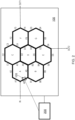
- Figure 1 shows a photonic circuit in general.
- a photonic circuit has a mesh of optical pathways formed of sections. These sections are formed by waveguides on a semiconductor substrate.
- the waveguides are formed on a silicon substrate.
- the semiconductor substrate is silicon
- a layer of SiO 2 is deposited on the Silicon and the sections of the optical pathway formed of Silicon or Silicon Nitrate (SiN) is formed within the SiO 2 to act as the section of the optical pathway.
- the disclosure is not so limited and may include Barium titanate (BTO) or Lithium niobate (LiNbOs) or the like.
- BTO Barium titanate
- LiNbOs Lithium niobate
- the photonic circuit has, in this case, one input (IN) and two outputs (OUT1 and OUT2).
- the constituent sections A6, B1, B6, B5, B4, D5, D4, F5 and F4 may be used.
- the optical pathway may be formed from constituent sections A 1, A2, A3, D2, D3, F5, F4.
- optical pathway between the input IN and output OUT2 is required.
- the optical light may follow a path along constituent sections A6, A5, B3, B4, EG, E5 or sections A1, A2, A3, A4, B3, B4, E6, E5. Again, there are many sections that may make up the optical pathway between the input and output OUT2.
- phase shifters and a tunable coupler which can be configured between a bar and cross-state in the constituent sections.
- the selection of the constituent sections used is arbitrary and simply the selection of an optical pathway is sufficient. This is particularly the case where the system is instructed to switch optical pathways between outputs (i.e. from OUT1 to OUT2 for example). In other words, it is the selection of any constituent sections that form the optical pathway between the input and output that is important rather than the specific constituent sections forming that pathway.
- the inventors have realised that with a configurable photonic circuit, it is desirable to select the most appropriate route between the input and either or both outputs. In other words, careful selection of the constituent sections forming the optical pathway can improve the performance of the configurable photonic circuit.
- the most appropriate route is selected based upon at least one property of the constituent sections making up the optical pathway. In embodiments, this at least one property is the optical loss along the respective constituent sections.
- the disclosure is not so limited and other criteria may be used when determining the most appropriate route. For example, the length of the constituent sections may be used as this would impact not only optical loss but also latency within the configurable photonic circuit as the further the light needs to travel, the higher the latency.
- Figure 2 shows a configurable photonic circuit 100 according to embodiments of the disclosure.
- a detector 105 is located on constituent section A6.
- the structure of the detector 105 according to embodiments will be described with reference to Figure 3 .
- the purpose of the detector 105 is to detect optical light emanating from the constituent section A6. This emanating optical light will form optical losses from the constituent section A6 which reduces the signal to noise ratio and increases cross-talk between the constituent sections.
- the detector 105 is therefore located along at least part of the constituent section A6 to measure the optical losses.
- the detector 105 may be located anywhere along the constituent section. However, in embodiments, the detector 105 may be located near junctions between different constituent sections. This is because the optical losses tend to be worse near to junctions and so placing detectors 105 so that the optical losses are measured at the junctions improves the determined optical pathway.
- FIG. 2 shows a single detector 105, it is envisaged that, in embodiments, there will be multiple detectors 105 and, in instances, one or more detectors 105 along each constituent section.
- Figure 3 shows a detector 105 according to embodiments. Although it is envisaged that any detector 105 that is capable of detecting and measuring the optical light emanating from the constituent section A6, the inventors have identified one particular type of detector 105 that is particularly useful.
- the detector 105 in embodiments will be formed of one or more graphene patch.
- a detector 105 formed of one or more graphene patch is particularly advantageous for a number of reasons. Firstly, graphene easily absorbs light in the range of 1 ⁇ m-3 ⁇ m. This wavelength of light is typically used in photonic circuits formed on a Silicon substrate. Further, graphene detectors are unbiased meaning that there is zero power consumption in the idle state. Furthermore, graphene detects high data rate signals due to its high electron mobility.
- a detector 105 is shown.
- the detector 105 sits above a waveguide shown which forms part of the constituent section A6.
- the detector 105 and has a source, drain and two gates (gate 1 and gate 2).
- a graphene patch 110 is positioned between the two gates and over the waveguide.
- the graphene patch 110 may be directly deposited on the SiOz layer or may be encapsulated to avoid contamination.
- the graphene patch may be encapsulated with Al 2 O 3 to preserve the layer of graphene and avoid contamination.
- a single patch of graphene is shown, the disclosure is not so limited and a multi-patch structure is envisaged which may be used to cover a more complex circuit.
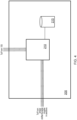
- controller 200 is connected to the configurable photonic circuit 100.
- the controller 200 is configured to control the operation of the configurable photonic circuit 100 by selecting the optical pathway and the constituent sections which form the optical pathway based upon, at least, the output of the or each detector 105.
- the controller 200 controls the tunable couplers and the phase shifters within the constituent sections of the optical pathway in the configurable photonic circuit 100 to control the flow of light through the constituent sections.
- the controller 200 includes connections to each of the detectors 105 within the configurable photonic circuit 100. This allows the output from each detector 105 to be provided to the controller 200 as will be explained later. Furthermore, the controller 200 includes connections to each of the constituent sections to control the phase shifters and/or tunable couplers within the constituent sections. It will be appreciated, that although Figure 4 shows a direct connection between the controller 200 and each detector 105 and the tunable couplers and phase shifters, the disclosure is not so limited and the controller 200 may be connected via any kind of arrangement and a direct connection is not required.
- a control section 210 is provided in the controller 200.
- the control section 210 is solid-state circuitry such as an Application Specific Integrated Circuit or, in embodiments, is circuitry whose operation is controlled using computer software.
- storage 215 is provided.
- the storage 215 is solid state circuitry configured to store data associated with each constituent section and computer readable code which, when loaded onto the control section 210 configures the control section 210 to perform steps according to embodiments of the disclosure.
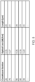
- Figure 5 shows a table that associates at least one property of the constituent section with the constituent section.
- the at least one property includes the optical loss along the constituent section and/or the length of the constituent section. It shall be noted that the disclosure is not limited to any one property of the constituent section and any one or more property may be chosen as will be appreciated Moreover, the one or more property of one or more constituent sections may be used to determine the optical pathway. For example, the optical loss across many constituent sections may be used to determine the optical pathway.
- the property of the constituent section is updated periodically. In embodiments, this update will occur regularly (maybe twice every second) or may occur when the difference between the stored value and the current value is above a threshold. For example, if the optical loss along a constituent section changes by greater than a threshold amount such as 0.05 dB/km is the property updated.
- the optical loss value will be provided by the detector 105 which is connected to the controller 200 and the controller 200 will update the stored optical loss value. In embodiments, the output from the detector 105 may be amplified before being provided to the controller 200.
- the length of the constituent section is unlikely to change as it is defined by the length of the waveguide.
- constituent section has been described as being part of a waveguide, the disclosure is not so limited.
- a constituent section may include any part of an optical pathway such as an optical switch or coupler or the like.
- the terms 'constituent section' may include any element that forms part of an optical pathway such as a waveguide (or part thereof), coupler, optical switch or the like.
- the graphene detector is used to measure the optical loss at the element.
- the disclosure is not so limited and the optical loss (or other property) may be determined at the constituent element using any appropriate mechanism.
- Figures 6A and 6B show a User Interface according to embodiments.
- the User Interface shows a schematic diagram of the photonic circuit with the input (IN) and outputs (OUT1 and OUT2).
- the disclosure is not so limited and the User Interface may be in any configuration that allows the user to control the controller 200.
- the User Interface is displayed on a display 600 that has a touch screen allowing the user to control the operation of the controller 200 using a touch screen.
- the disclosure is not so limited and any type of display and user control element (such as a mouse or the like) is envisaged.
- the user touches the input (in Figure 6A ) and then touches one of the outputs. In this case, the user touches OUT1.
- This user control instructs the controller 200 to create an optical pathway between IN and OUT1.
- any equivalent control is envisaged and any number of input(s) and/or output(s) is envisaged.
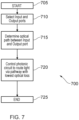
- Figure 7 shows a process 700 according to embodiments which is performed by the controller 200.
- the process starts at step 705.
- the process then moves to step 710 where the input and output port is selected.
- this is performed by the user, but in embodiments, this is performed by an external controller which selects the input and output ports based on one or more other criteria such as routing an input optical fibre port to a different optical fibre output port.
- step 715 the various paths between the selected input port and output port are processed so that one optical pathway is determined.
- This may be performed, in embodiments, using Dijkstra's algorithm whereby the property or properties of interest are used as the cost of a vector.
- the optical loss property will provide a cost of each vector and in embodiments, the length of each constituent section will also provide a cost of each vector.
- the disclosure is not so limited and any property or properties may provide a cost of each vector.
- the disclosure is not limited to using Dijkstra's algorithm and any suitable routing algorithm is envisaged.
- step 720 the controller 200 controls the photonic circuit to route the light via a pathway having the lowest cost.
- the controller will control the photonic circuit to route the light according to the property which is used in the Dijkstra algorithm.
- this control will be performed by controlling the phase shifters and/or tunable couplers (not shown) which are provided within a photonic circuit. This control of the phase shifters and tunable couplers is using known techniques.
- step 725 where the process 700 ends.
- the controller 200 In addition to establishing the optical pathway between an input and an output (or between a plurality of inputs and outputs), in embodiments, the controller 200 also controls the output power of the input emitter. This control may be via direct control of the input emitter or by issuing commands to the input emitter.
- the term 'input emitter' means the provider of the optical light at the input port, which, in embodiments, is a laser.
- the controller 200 informs the input emitter of the optical power required at the input port to achieve a given output optical power. This allows the input emitter to dynamically change the input optical power to achieve a certain output laser power. This improves energy efficiency of the system whilst ensuring there is sufficient optical power for an output port.
- optical loss as the property, the disclosure is not so limited and any property is envisaged.
- the optical loss for each constituent section is stored and compared with the previous iteration of the manufacturing process.
- the level of SiN doping used in the constituent sections of the optical pathways may be different to the level of SiN doping in the current iteration. Accordingly, it is possible to evaluate whether, for example, the previous level or the current level of doping is better.
- Described embodiments may be implemented in any suitable form including hardware, software, firmware or any combination of these. Described embodiments may optionally be implemented at least partly as computer software running on one or more data processors and/or digital signal processors.
- the elements and components of any embodiment may be physically, functionally and logically implemented in any suitable way. Indeed the functionality may be implemented in a single unit, in a plurality of units or as part of other functional units. As such, the disclosed embodiments may be implemented in a single unit or may be physically and functionally distributed between different units, circuitry and/or processors.
Landscapes
- Physics & Mathematics (AREA)
- General Physics & Mathematics (AREA)
- Optics & Photonics (AREA)
- Engineering & Computer Science (AREA)
- Microelectronics & Electronic Packaging (AREA)
- Mathematical Physics (AREA)
- Computer Networks & Wireless Communication (AREA)
- Computing Systems (AREA)
- Electromagnetism (AREA)
- Signal Processing (AREA)
- Computer Hardware Design (AREA)
- General Engineering & Computer Science (AREA)
- Optical Integrated Circuits (AREA)
- Photometry And Measurement Of Optical Pulse Characteristics (AREA)
Applications Claiming Priority (1)
| Application Number | Priority Date | Filing Date | Title |
|---|---|---|---|
| GB2319997.9A GB2636854A (en) | 2023-12-22 | 2023-12-22 | A device, computer program and method |
Publications (1)
| Publication Number | Publication Date |
|---|---|
| EP4575601A1 true EP4575601A1 (de) | 2025-06-25 |
Family
ID=89767991
Family Applications (1)
| Application Number | Title | Priority Date | Filing Date |
|---|---|---|---|
| EP24219212.8A Pending EP4575601A1 (de) | 2023-12-22 | 2024-12-11 | Vorrichtung, computerprogramm und verfahren |
Country Status (4)
| Country | Link |
|---|---|
| US (1) | US20250208340A1 (de) |
| EP (1) | EP4575601A1 (de) |
| CN (1) | CN120201333A (de) |
| GB (1) | GB2636854A (de) |
Citations (5)
| Publication number | Priority date | Publication date | Assignee | Title |
|---|---|---|---|---|
| US20210333818A1 (en) * | 2020-04-27 | 2021-10-28 | Lightmatter, Inc. | Photonics processor architecture |
| US20220413222A1 (en) * | 2019-05-09 | 2022-12-29 | Universitat Politècnica De València | Photonic chip, field programmable photonic array and photonic integrated circuit |
| US20230029063A1 (en) * | 2019-12-18 | 2023-01-26 | Universitat Politecnica De Valencia | Integrated photonic device comprising a field-programmable photonic gate array, a quantum device and programmable circuits |
| US20230251423A1 (en) * | 2020-07-16 | 2023-08-10 | Universitat Politècnica De València | Programmable photonic integrated circuit and related method of operation |
| US20230366913A1 (en) * | 2020-09-28 | 2023-11-16 | Psiquantum, Corp. | Method and structure to incorporate multiple low loss photonic circuit components |
-
2023
- 2023-12-22 GB GB2319997.9A patent/GB2636854A/en active Pending
-
2024
- 2024-12-11 EP EP24219212.8A patent/EP4575601A1/de active Pending
- 2024-12-13 CN CN202411842085.8A patent/CN120201333A/zh active Pending
- 2024-12-14 US US18/981,477 patent/US20250208340A1/en active Pending
Patent Citations (5)
| Publication number | Priority date | Publication date | Assignee | Title |
|---|---|---|---|---|
| US20220413222A1 (en) * | 2019-05-09 | 2022-12-29 | Universitat Politècnica De València | Photonic chip, field programmable photonic array and photonic integrated circuit |
| US20230029063A1 (en) * | 2019-12-18 | 2023-01-26 | Universitat Politecnica De Valencia | Integrated photonic device comprising a field-programmable photonic gate array, a quantum device and programmable circuits |
| US20210333818A1 (en) * | 2020-04-27 | 2021-10-28 | Lightmatter, Inc. | Photonics processor architecture |
| US20230251423A1 (en) * | 2020-07-16 | 2023-08-10 | Universitat Politècnica De València | Programmable photonic integrated circuit and related method of operation |
| US20230366913A1 (en) * | 2020-09-28 | 2023-11-16 | Psiquantum, Corp. | Method and structure to incorporate multiple low loss photonic circuit components |
Non-Patent Citations (3)
| Title |
|---|
| "European Horizon", 2020, SCUOLA SUPERIORE SANT'ANNA |
| CHEN XIANGFENG ET AL: "Graph Representations for Programmable Photonic Circuits", JOURNAL OF LIGHTWAVE TECHNOLOGY, IEEE, USA, vol. 38, no. 15, 3 April 2020 (2020-04-03), pages 4009 - 4018, XP011800056, ISSN: 0733-8724, [retrieved on 20200721], DOI: 10.1109/JLT.2020.2984990 * |
| S. MARCONIA. GIAMBRA ET AL., NATURE COMMUNICATIONS, Retrieved from the Internet <URL:https://doi.org/10.1038/s41467-021-21137-z> |
Also Published As
| Publication number | Publication date |
|---|---|
| GB202319997D0 (en) | 2024-02-07 |
| US20250208340A1 (en) | 2025-06-26 |
| CN120201333A (zh) | 2025-06-24 |
| GB2636854A (en) | 2025-07-02 |
Similar Documents
| Publication | Publication Date | Title |
|---|---|---|
| US20250341675A1 (en) | Photonic communication platform | |
| Smit et al. | Past, present, and future of InP-based photonic integration | |
| US7251386B1 (en) | Integrated photonic-electronic circuits and systems | |
| US6583645B1 (en) | Field programmable optical arrays | |
| US10684497B2 (en) | Electro-optic modulator | |
| CN114563845B (zh) | 一种非对称定向耦合器及可调控模式产生器、光环行器 | |
| WO2015139584A1 (en) | Apparatus and method for feedback system for optical switch controller | |
| Temporiti et al. | A 3D-integrated 25Gbps silicon photonics receiver in PIC25G and 65nm CMOS technologies | |
| CN113191115A (zh) | 基于dbs算法的可编程任意功率分配器 | |
| CN103326781B (zh) | 光交换设备和方法 | |
| CN112087259A (zh) | 一种光交换网络的检测方法 | |
| EP4575601A1 (de) | Vorrichtung, computerprogramm und verfahren | |
| de Cea et al. | Single-mode waveguide-coupled light emitting diodes in unmodified silicon photonics fabrication processes | |
| CN114740341B (zh) | 一种光开关切换延时线中光开关控制电压的标定方法 | |
| Ian et al. | Advanced research in on-chip optical interconnects | |
| CN217561775U (zh) | 一种非对称定向耦合器及可调控模式产生器、光环行器 | |
| WO2015161537A1 (zh) | 微环光开关芯片的设计方法 | |
| CN114253010A (zh) | 一种微环调制器 | |
| CN105810774A (zh) | 一种高功率大带宽锗硅光电探测器 | |
| Dumais et al. | Scaling up silicon photonic switch fabrics | |
| CN110191379B (zh) | 光缓存芯片及电子设备 | |
| Suzuki et al. | Broadband 8x8 Si-wire PILOSS switch with double Mach-Zehnder switch elements | |
| JP2009152357A (ja) | 半導体基板の処理方法および半導体基板の処理装置 | |
| EP3726753A1 (de) | Optisches multi-bit-rechnersystem | |
| KR20210031346A (ko) | 실리콘 기반 광 변조 장치 |
Legal Events
| Date | Code | Title | Description |
|---|---|---|---|
| PUAI | Public reference made under article 153(3) epc to a published international application that has entered the european phase |
Free format text: ORIGINAL CODE: 0009012 |
|
| STAA | Information on the status of an ep patent application or granted ep patent |
Free format text: STATUS: REQUEST FOR EXAMINATION WAS MADE |
|
| 17P | Request for examination filed |
Effective date: 20241211 |
|
| AK | Designated contracting states |
Kind code of ref document: A1 Designated state(s): AL AT BE BG CH CY CZ DE DK EE ES FI FR GB GR HR HU IE IS IT LI LT LU LV MC ME MK MT NL NO PL PT RO RS SE SI SK SM TR |