EP4572075A1 - Stromversorgungsschaltung mit mehreren eingängen und elektronische vorrichtung - Google Patents
Stromversorgungsschaltung mit mehreren eingängen und elektronische vorrichtung Download PDFInfo
- Publication number
- EP4572075A1 EP4572075A1 EP23869756.9A EP23869756A EP4572075A1 EP 4572075 A1 EP4572075 A1 EP 4572075A1 EP 23869756 A EP23869756 A EP 23869756A EP 4572075 A1 EP4572075 A1 EP 4572075A1
- Authority
- EP
- European Patent Office
- Prior art keywords
- input
- voltage
- circuit
- power supply
- switch
- Prior art date
- Legal status (The legal status is an assumption and is not a legal conclusion. Google has not performed a legal analysis and makes no representation as to the accuracy of the status listed.)
- Pending
Links
Images


Classifications
-
- H—ELECTRICITY
- H02—GENERATION; CONVERSION OR DISTRIBUTION OF ELECTRIC POWER
- H02J—CIRCUIT ARRANGEMENTS OR SYSTEMS FOR SUPPLYING OR DISTRIBUTING ELECTRIC POWER; SYSTEMS FOR STORING ELECTRIC ENERGY
- H02J4/00—Circuit arrangements for mains or distribution networks not specified as AC or DC
-
- H—ELECTRICITY
- H02—GENERATION; CONVERSION OR DISTRIBUTION OF ELECTRIC POWER
- H02M—APPARATUS FOR CONVERSION BETWEEN AC AND AC, BETWEEN AC AND DC, OR BETWEEN DC AND DC, AND FOR USE WITH MAINS OR SIMILAR POWER SUPPLY SYSTEMS; CONVERSION OF DC OR AC INPUT POWER INTO SURGE OUTPUT POWER; CONTROL OR REGULATION THEREOF
- H02M1/00—Details of apparatus for conversion
- H02M1/42—Circuits or arrangements for compensating for or adjusting power factor in converters or inverters
- H02M1/4208—Arrangements for improving power factor of AC input
-
- G—PHYSICS
- G11—INFORMATION STORAGE
- G11C—STATIC STORES
- G11C7/00—Arrangements for writing information into, or reading information out from, a digital store
- G11C7/06—Sense amplifiers; Associated circuits, e.g. timing or triggering circuits
-
- H—ELECTRICITY
- H02—GENERATION; CONVERSION OR DISTRIBUTION OF ELECTRIC POWER
- H02J—CIRCUIT ARRANGEMENTS OR SYSTEMS FOR SUPPLYING OR DISTRIBUTING ELECTRIC POWER; SYSTEMS FOR STORING ELECTRIC ENERGY
- H02J1/00—Circuit arrangements for DC mains or DC distribution networks
- H02J1/10—Parallel operation of DC sources
-
- H—ELECTRICITY
- H02—GENERATION; CONVERSION OR DISTRIBUTION OF ELECTRIC POWER
- H02M—APPARATUS FOR CONVERSION BETWEEN AC AND AC, BETWEEN AC AND DC, OR BETWEEN DC AND DC, AND FOR USE WITH MAINS OR SIMILAR POWER SUPPLY SYSTEMS; CONVERSION OF DC OR AC INPUT POWER INTO SURGE OUTPUT POWER; CONTROL OR REGULATION THEREOF
- H02M1/00—Details of apparatus for conversion
- H02M1/0003—Details of control, feedback or regulation circuits
- H02M1/0032—Control circuits allowing low power mode operation, e.g. in standby mode
-
- H—ELECTRICITY
- H02—GENERATION; CONVERSION OR DISTRIBUTION OF ELECTRIC POWER
- H02M—APPARATUS FOR CONVERSION BETWEEN AC AND AC, BETWEEN AC AND DC, OR BETWEEN DC AND DC, AND FOR USE WITH MAINS OR SIMILAR POWER SUPPLY SYSTEMS; CONVERSION OF DC OR AC INPUT POWER INTO SURGE OUTPUT POWER; CONTROL OR REGULATION THEREOF
- H02M1/00—Details of apparatus for conversion
- H02M1/10—Arrangements incorporating converting means for enabling loads to be operated at will from different kinds of power supplies, e.g. from AC or DC
-
- H—ELECTRICITY
- H02—GENERATION; CONVERSION OR DISTRIBUTION OF ELECTRIC POWER
- H02M—APPARATUS FOR CONVERSION BETWEEN AC AND AC, BETWEEN AC AND DC, OR BETWEEN DC AND DC, AND FOR USE WITH MAINS OR SIMILAR POWER SUPPLY SYSTEMS; CONVERSION OF DC OR AC INPUT POWER INTO SURGE OUTPUT POWER; CONTROL OR REGULATION THEREOF
- H02M1/00—Details of apparatus for conversion
- H02M1/32—Means for protecting converters other than automatic disconnection
-
- H—ELECTRICITY
- H02—GENERATION; CONVERSION OR DISTRIBUTION OF ELECTRIC POWER
- H02M—APPARATUS FOR CONVERSION BETWEEN AC AND AC, BETWEEN AC AND DC, OR BETWEEN DC AND DC, AND FOR USE WITH MAINS OR SIMILAR POWER SUPPLY SYSTEMS; CONVERSION OF DC OR AC INPUT POWER INTO SURGE OUTPUT POWER; CONTROL OR REGULATION THEREOF
- H02M3/00—Conversion of DC power input into DC power output
- H02M3/02—Conversion of DC power input into DC power output without intermediate conversion into AC
- H02M3/04—Conversion of DC power input into DC power output without intermediate conversion into AC by static converters
- H02M3/10—Conversion of DC power input into DC power output without intermediate conversion into AC by static converters using discharge tubes with control electrode or semiconductor devices with control electrode
- H02M3/145—Conversion of DC power input into DC power output without intermediate conversion into AC by static converters using discharge tubes with control electrode or semiconductor devices with control electrode using devices of a triode or transistor type requiring continuous application of a control signal
- H02M3/155—Conversion of DC power input into DC power output without intermediate conversion into AC by static converters using discharge tubes with control electrode or semiconductor devices with control electrode using devices of a triode or transistor type requiring continuous application of a control signal using semiconductor devices only
- H02M3/156—Conversion of DC power input into DC power output without intermediate conversion into AC by static converters using discharge tubes with control electrode or semiconductor devices with control electrode using devices of a triode or transistor type requiring continuous application of a control signal using semiconductor devices only with automatic control of output voltage or current, e.g. switching regulators
- H02M3/158—Conversion of DC power input into DC power output without intermediate conversion into AC by static converters using discharge tubes with control electrode or semiconductor devices with control electrode using devices of a triode or transistor type requiring continuous application of a control signal using semiconductor devices only with automatic control of output voltage or current, e.g. switching regulators including plural semiconductor devices as final control devices for a single load
Definitions
- This application relates to the field of power supply technologies, and in particular, to a multi-input power supply circuit and an electronic device.
- An electronic device includes a power supply circuit and a load.
- the power supply circuit is configured to receive an input voltage provided by an external power supply, process the input voltage, and then provide an output voltage for the load, to drive the load to operate.
- a multi-input power supply circuit is a power supply circuit that can simultaneously receive a plurality of input voltages.
- the multi-input power supply circuit receives the plurality of input voltages respectively through a plurality of input interfaces, and provides an output voltage for the load based on one of the input voltages.
- the multi-input power supply circuit further includes a sampling circuit and a control circuit.
- the sampling circuit includes isolators such as optocouplers, isolated power supplies that supply power to the isolators, and the like.
- the isolator may sample voltage values of the plurality of input voltages, and send feedback signals to the control circuit.
- the control circuit controls, based on the feedback signal, an input interface of one of the input voltages to be connected to the power conversion circuit, so that the power conversion circuit processes the input voltage and then provides an output voltage for the load.
- This application provides a multi-input power supply circuit and an electronic device, to resolve a technical problem of high complexity of a structure of a multi-input power supply circuit in the conventional technology.
- a first aspect of this application provides a multi-input power supply circuit, including a plurality of input interfaces, a first switch, a power conversion circuit, a sampling circuit, and a control circuit.
- the sampling circuit includes at least one resistor.
- the at least one resistor is configured to: provide a voltage feedback signal for the control circuit based on voltage values of input voltages of the plurality of input interfaces; and provide a function of isolation between the control circuit and the input interfaces.
- the control circuit controls the first switch based on the voltage feedback signals. For example, the control circuit controls an input end of the first switch to be connected to an output end, so that the power conversion circuit provides an output voltage for a load based on the input voltages provided by the input interfaces.
- the sampling circuit may implement functions of input voltage sampling and isolation by using the at least one resistor. Therefore, complexity of a circuit structure of the sampling circuit is low, thereby reducing the complexity and costs of the circuit structure of the multi-input power supply circuit.
- the at least one resistor in the sampling circuit does not introduce more interference, and overall reliability of the multi-input power supply circuit can also be improved.
- the sampling circuit specifically includes a plurality of sampling subcircuits, and each sampling subcircuit includes a plurality of resistors that are connected in series.
- An input end of the plurality of resistors that are connected in series may be configured to connect to a positive electrode or a negative electrode of one input interface, and an output end of the plurality of resistors that are connected in series is connected to the control circuit.
- the plurality of resistors may be configured to provide a voltage feedback signal for the control circuit based on a voltage value of the connected positive electrode or negative electrode.
- the sampling circuit may implement the sampling and isolation functions by using the plurality of resistors that are connected in series. Even if the multi-input power supply circuit has more input interfaces, only a resistor needs to be added to the sampling circuit, thereby greatly reducing the complexity of the structure of the multi-input power supply circuit.
- the multi-input power supply circuit is disposed between the control circuit and the plurality of sampling subcircuits; and may be configured to: amplify a voltage feedback signal provided by the sampling subcircuit, and provide an amplified voltage feedback signal for the control circuit.
- the sampling circuit can provide, for the control circuit, a voltage feedback signal that is more suitable for processing by the control circuit, thereby improving processing efficiency and stability of the control circuit.
- the multi-input power supply circuit further includes a second switch.
- the control circuit may control an input end, corresponding to an input interface, of the second switch to be connected to an output end of the second switch.
- the sampling circuit can provide, through the second switch, a voltage feedback signal for the control circuit based on an input voltage of the input interface, and the control circuit can determine a voltage value of the input voltage of the input interface based on the voltage feedback signal. Therefore, in the multi-input power supply circuit provided in this embodiment, only two sampling subcircuits need to be disposed, and the sampling subcircuits are controlled, by using the second switch, to be connected to different input interfaces.
- the sampling circuit specifically includes a plurality of variable resistors.
- the sampling circuit provides, by using the plurality of variable resistors, the voltage feedback signal for the control circuit based on the input voltages of the input interfaces, and provides the function of isolation between the control circuit and the input interfaces.
- the sampling circuit also has the sampling and isolation functions, and the complexity of the structure of the circuit is further greatly reduced. Even if the multi-input power supply circuit has more input interfaces, only a variable resistor needs to be added to the sampling circuit.
- variable resistors may be adjusted based on input voltages of input ends of the variable resistors, thereby improving flexibility of the multi-input power supply circuit. Therefore, the multi-input power supply circuit can be used in more different scenarios such as a scenario of a variable input voltage, thereby enriching functions and application scenarios of the multi-input power supply circuit.
- the control circuit may specifically respond to a case in which a voltage value of an input voltage of a first input interface in the plurality of input interfaces is within an operating voltage range required by the load, and then the control circuit controls a first input end, corresponding to the first input interface, of the first switch to be connected to an output end of the first switch. Therefore, an input voltage that is provided by a power supply and that meets an operating requirement of the load can be determined from input voltages provided by a plurality of power supplies, to supply power to the load, thereby ensuring stable operation of the load.
- the control circuit may specifically respond to a case in which the voltage value of the input voltage of the first input interface in the plurality of input interfaces is not within the operating voltage range required by the load, and then the control circuit controls a second input end, corresponding to a second input interface, of the first switch to be connected to the output end of the first switch. Therefore, when the plurality of power supplies provides the input voltages, and an input voltage provided by one power supply cannot drive the load to operate normally, switching to an input voltage provided by another power supply can be performed in time, to supply power to the load, thereby ensuring continuous and stable operation of the load.
- the control circuit may specifically respond to a case in which the voltage values of the input voltages of all the plurality of input interfaces in the plurality of input interfaces are not within the operating voltage range required by the load, and then the control circuit controls the plurality of input ends of the first switch to be all disconnected from the output end of the first switch. Therefore, when none of the input voltages provided by the plurality of power supplies can drive the load to operate normally, the first switch may be controlled to disconnect in time the input voltages provided by all the power supplies. This provides protection for the multi-input power supply circuit and the subsequent load, thereby improving safety of the multi-input power supply circuit.
- the control circuit may respond to a case in which the voltage values of the input voltages of all the plurality of input interfaces in the plurality of input interfaces are not within the operating voltage range required by the load and a sum of voltage values of a plurality of target input interfaces in the plurality of input interfaces is within the required operating voltage range, and then the control circuit controls the input ends, corresponding to the plurality of target input interfaces, of the first switch to be connected in series, and then connects the plurality of target input interfaces to the output end of the first switch after the series connection. Therefore, the load can still operate continuously and normally when none of the input voltages provided by all the power supplies is within the operating voltage range.
- the power conversion circuit of the multi-input power supply circuit specifically includes a power factor correction circuit and a direct current conversion circuit.
- control circuit may be integrated into the power factor correction circuit or the direct current conversion circuit, so that the multi-input power supply circuit has higher integration, thereby further reducing the complexity of the structure of the multi-input power supply circuit.
- input voltages of the multi-input power supply circuit are alternating-current or direct-current.
- the multi-input power supply circuit provided in this embodiment is highly flexible, and can be used in different scenarios.
- a second aspect of this application provides an electronic device, including a load and the multi-input power supply circuit according to any one of the embodiments of the first aspect of this application.
- the multi-input power supply circuit is connected to a plurality of power supplies; and may be configured to obtain an input voltage provided by any one of the plurality of power supplies, process the input voltage, and provide an output voltage for the load.
- a process, method, system, product, or device that includes a list of steps or units is not necessarily limited to those steps or units that are expressly listed, but may include other steps or units that are not expressly listed or inherent to such a process, method, product, or device.
- a connection relationship described in this application means a direct or an indirect connection.
- that A is connected to B may be that A is directly connected to B, or that A is indirectly connected to B through one or more other electrical components.
- that A is indirectly connected to B may be that A is directly connected to C, and C is directly connected to B. In this way, A is connected to B through C.
- “A is connected to B" described in this application may be that A is directly connected to B, or may be that A is indirectly connected to B through one or more other electrical components.
- FIG. 1 is a diagram of a structure of an electronic device according to an embodiment of this application.
- the electronic device 1 shown in FIG. 1 includes a multi-input power supply circuit 10 and a load 20.
- the multi-input power supply 10 is configured to supply power to the load 20 in the electronic device 1.
- the electronic device shown in FIG. 1 may be an electrical device such as a network device, a mobile phone, a notebook computer, a computer case, a television, a smart tablet, an interactive tablet, an electric vehicle, a smart furniture device, a smartwatch, or a wearable device.
- FIG. 2 is a diagram of another structure of an electronic device according to an embodiment of this application.
- the electronic device 1 shown in FIG. 2 includes a multi-input power supply circuit 10.
- the multi-input power supply circuit 10 is configured to supply power to a load 20 outside the electronic device 1.
- the electronic device 1 shown in FIG. 2 may be a power supply device such as a power adapter, a charger, a vehicle charging station, or a mobile power supply.
- the multi-input power supply circuit 10 may be configured to receive input voltages provided by a plurality of power supplies. For example, in the examples shown in FIG. 1 and FIG. 2 , the multi-input power supply circuit 10 may be configured to receive an input voltage V A provided by a power supply A, an input voltage V B provided by a power supply B, ..., an input voltage V N provided by a power supply N, and the like. The multi-input power supply circuit 10 may perform processing such as power factor correction and voltage conversion on one of the input voltages provided by one power supply, and then provide an output voltage Vo for the load 20 to supply power to the load 20.
- an input voltage may be provided by an external power supply of the electronic device 1, or may be provided by an internal power supply of the electronic device 1.
- the multi-input power supply circuit 10 can simultaneously receive the input voltages provided by the plurality of power supplies, when a power supply in the plurality of power supplies is faulty, the multi-input power supply circuit 10 can also continue to supply power to the load 20 based on an input voltage provided by another power supply that is not faulty.
- the multi-input power supply circuit 10 is highly reliable, and can ensure continuous and stable running of the load 20.
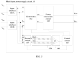
- FIG. 3 is a diagram of a structure of a multi-input power supply circuit according to an embodiment of this application.
- FIG. 3 shows a specific implementation of the multi-input power supply circuit 10 shown in FIG. 1 and FIG. 2 .
- the multi-input power supply circuit 10 includes a plurality of input interfaces 101, a first switch 102, a power conversion circuit 103, a sampling circuit 104, and a control circuit 105.
- a plurality of input ends of the first switch 102 are respectively connected to the plurality of input interfaces 101.
- an input end a of the first switch 102 provided in FIG. 3 is connected to an input interface 101A.
- the first switch 102 may receive, through the input interface 101A, an input voltage V A provided by a power supply A.
- An input end b of the first switch 102 is connected to an input interface 101B.
- the first switch 102 may receive, through the input interface 101B, an input voltage V B provided by a power supply B.
- the rest can be deduced by analogy.
- the first switch 102 has n input ends, and the n input ends may be configured to respectively connect to N input interfaces 101A to 101N is used as an example.
- a quantity of input ends of the first switch 102, a quantity of input interfaces 101 connected to the first switch 102, and a quantity of power supplies connected to the first switch 102 through the input interfaces 101 are not limited in this embodiment of this application.
- a plurality of input voltages of the multi-input power supply circuit 10 may be direct-current, and an output voltage of the multi-input power supply circuit may be direct-current.
- input voltages of the multi-input power supply circuit 10 may be alternating-current.
- the multi-input power supply circuit 10 may further perform voltage conversion on the alternating currents, and provide an output voltage Vo in a direct-current form.
- An output end o of the first switch 102 is connected to an input end of the power conversion circuit 103.
- the first switch 102 may be configured to connect one input end to the output end o of the first switch 102.
- the power conversion circuit 103 can receive, through the output end o of the first switch 102 and an input interface 101 connected to the connected input end, an input voltage by using the first switch 102 and the input interface 101.
- the power conversion circuit 103 may receive, through the output end o of the first switch 102 and the input interface 101A connected to the input end a of the first switch 102, the input voltage V A provided by the power supply A.
- the power conversion circuit 103 may be configured to: perform processing such as power factor correction and voltage conversion on the input voltage, and then provide the output voltage Vo.
- the power conversion circuit 103 includes a power factor correction (power factor correction, PFC) circuit and a direct current conversion (Direct Current-Direct Current, DC-DC) circuit.
- the power factor correction circuit is configured to adjust a power factor (power factor, PF) of an input voltage
- the direct current conversion circuit is configured to perform voltage conversion processing on the input voltage to obtain the output voltage Vo.
- a voltage value of the input voltage of the multi-input power supply circuit 10 is different from a voltage value of the output voltage Vo.
- a plurality of input ends of the sampling circuit 104 are respectively connected to the plurality of output interfaces 101, and an output end of the sampling circuit 104 is connected to the control circuit 105.
- the sampling circuit 104 is configured to send voltage feedback signals to the control circuit 105 based on voltage values of input voltages of the plurality of input interfaces 101.
- the voltage feedback signals are used to indicate the voltage values of the plurality of input voltages of the multi-input power supply circuit 10.
- the control circuit 105 is connected to the sampling circuit 104 and the first switch 102.
- the control circuit 105 may be configured to control the first switch 102.
- the control circuit 105 may receive the voltage feedback signals sent by the sampling circuit 104, and control one input end of the first switch 102 to be connected to the output end o of the first switch 102 based on the voltage feedback signals.
- control circuit 105 is further connected to the power conversion circuit 103.
- the control circuit 105 may be configured to control the power conversion circuit 103.
- control circuit 105 may be configured to control on/off of a switch transistor in the power conversion circuit 103, so that the power conversion circuit 103 performs processing such as voltage conversion on the input voltage received by the input end of the power conversion circuit 103, to obtain the output voltage Vo.
- control circuit 105 may be a pulse-width modulation (Pulse-width modulation, PWM) controller, a central processing unit (central processing unit, CPU), another general-purpose processor, a digital signal processor (digital signal processor, DSP), an application-specific integrated circuit (application-specific integrated circuit, ASIC), a field-programmable gate array (field-programmable gate array, FPGA) or another programmable logic device, a discrete gate or a transistor logic device, or the like.
- PWM pulse-width modulation
- CPU central processing unit
- DSP digital signal processor
- ASIC application-specific integrated circuit
- FPGA field-programmable gate array
- FPGA field-programmable gate array
- control circuit 105 may be dedicated to controlling the first switch 102.
- control circuit 105 may be integrated into the power factor correction circuit, and the control circuit 105 may be configured to control the first switch 102 and the power factor correction circuit.
- control circuit 105 may be integrated into the direct current conversion circuit, and the control circuit 105 may be configured to control the first switch 102 and the direct current conversion circuit.
- control circuit 105 may be integrated into the power conversion circuit 103, and the control circuit 105 may be configured to control the first switch 102 and the power conversion circuit 103.
- the voltage values of the input voltages of the input interfaces 101 of the multi-input power supply circuit 10 are relatively large, and a voltage value within a voltage range of a voltage signal that can be processed by the control circuit 105 is relatively small. Therefore, the sampling circuit 104 further has an isolation function, so that safety and reliability of the control circuit 105 and the multi-input power supply circuit 10 in which the control circuit 105 is located can be improved. For example, a voltage value of an input voltage received by the input end of the sampling circuit 104 is relatively large.
- the sampling circuit 104 may be configured to: perform voltage conversion processing on the input voltage to obtain a voltage feedback signal of a relatively small voltage value, and send the voltage feedback signal of the relatively small voltage value to the control circuit 105, so that the control circuit 105 can process the voltage feedback signal within a safe voltage range.
- the sampling circuit 104 includes isolators such as optocouplers, and further includes isolated power supplies that supply power to the isolators, and the like.
- the optocouplers in the sampling circuit 104 may implement both the following functions: a function of performing sampling processing on the input voltages of the input interfaces 101 to obtain the voltage feedback signals, and a function of isolation between the control circuit 105 and the input interfaces 101.
- a corresponding isolator and a corresponding isolated power supply need to be disposed in the sampling circuit 104 for each input interface 101.
- this application provides a multi-input power supply circuit 10, to reduce the complexity of the structure of the multi-input power supply circuit 10.
- the following describes the technical solutions of this application in detail by using specific embodiments. The following several specific embodiments may be combined with each other, and a same or similar concept or process may not be described repeatedly in some embodiments.
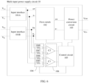
- FIG. 4 is a diagram of a structure of a multi-input power supply circuit according to an embodiment of this application.
- the multi-input power supply circuit 10 shown in FIG. 4 includes a plurality of input interfaces 101, a first switch 102, a power conversion circuit 103, a sampling circuit 104, and a control circuit 105.
- the multi-input power supply circuit 10 includes two input interfaces 101A and 101B.
- Two input ends of the input interface 101A are respectively configured to receive a positive voltage V A + and a negative voltage V A - of an input voltage V A provided by a power supply A.
- Two input ends of the input interface 101B are respectively configured to receive a positive voltage V B + and a negative voltage V B - of an input voltage V B provided by a power supply B.
- An input end a+ and an input end a- of the first switch 102 are connected to the input interface 101A, and the first switch 102 may receive, through the input interface 101A, the input voltage V A provided by the power supply A.
- An input end b+ and an input end b- of the first switch are connected to the input interface 101B, and the first switch 102 may receive, through the input interface 101B, the input voltage V B provided by the power supply B.
- a positive output end o+ and a negative output end o- of the first switch 102 are respectively connected to input ends of the power conversion circuit 103.
- the first switch 102 may be configured to connect the input end a+ to the positive output end o+, and connect the input end a- to the negative output end o-, so that the power conversion circuit 103 can receive the input voltage V A through the first switch 102 and the input interface 101A.
- the first switch 102 may be configured to connect the input end b+ to the positive output end o+, and connect the input end b- to the negative output end o-, so that the power conversion circuit 103 can receive the input voltage V B through the first switch 102 and the input interface 101B.
- the power conversion circuit 103 may be configured to: perform processing such as power factor correction and voltage conversion on the received input voltage V A or the input voltage V B , and then provide an output voltage Vo.
- the sampling circuit 104 includes a plurality of sampling subcircuits.
- Each sampling subcircuit includes a plurality of resistors that are connected in series. An input end of the plurality of resistors that are connected in series is connected to a positive electrode or a negative electrode of an input interface 101, and an output end of the plurality of resistors is connected to the control circuit 105.
- the multi-input power supply circuit 10 further includes a plurality of operational amplifiers. A positive input end and a negative input end of each operational amplifier are respectively connected, through one sampling subcircuit, to a positive electrode and a negative electrode that correspond to a same input interface.
- the sampling circuit 104 includes four sampling subcircuits that are denoted as a first sampling subcircuit 1041, a second sampling subcircuit 1042, a third sampling subcircuit 1043, and a fourth sampling subcircuit 1044.
- the first sampling subcircuit 1041 includes four resistors R1 to R4 that are connected in series. In the first sampling subcircuit 1041, one end of a resistor R1 is used as an input end, and one end of a resistor R4 is used as an output end.
- the input end of the first sampling subcircuit 1041 is connected to the positive electrode V A + of the input interface 101A, and the output end of the first sampling subcircuit 1041 is connected to a positive electrode of a first operational amplifier C1.
- an input end of the second sampling subcircuit 1042 is connected to the negative electrode V A - of the input interface 101A, and an output end of the second sampling subcircuit 1042 is connected to a negative electrode of the first operational amplifier C1.
- An output end of the first operational amplifier C1 is connected to the control circuit 105.
- an input end of the third sampling subcircuit 1043 is connected to the positive electrode V B + of the input interface 101B, and an output end of the third sampling subcircuit 1043 is connected to a positive electrode of a first operational amplifier C2.
- An input end of the fourth sampling subcircuit 1044 is connected to the negative electrode V B - of the input interface 101B, and an output end of the fourth sampling subcircuit 1044 is connected to a negative electrode of the second operational amplifier C2.
- An output end of the second operational amplifier C2 is connected to the control circuit 105.
- the positive voltage V A + of the input end of the first sampling subcircuit 1041 is divided by the four resistors R1 to R4 to obtain a first voltage feedback signal, and the input end of the first sampling subcircuit 1041 outputs the first voltage feedback signal to the positive electrode of the first operational amplifier C1.
- the negative voltage V A - of the input end of the second sampling subcircuit 1042 is divided by four resistors R1 to R4 to obtain a second voltage feedback signal, and the input end of the second sampling subcircuit 1042 outputs the second voltage feedback signal to the negative electrode of the first operational amplifier C1.
- the first operational amplifier C1 provides, based on the first voltage feedback signal and the second voltage feedback signal, an amplified voltage feedback signal of the input voltage V A for the control circuit 105.
- the voltage feedback signal is used to indicate a voltage value of the input voltage V A provided by the power supply A.
- the second operational amplifier C2 provides an amplified voltage feedback signal of the input voltage V B for the control circuit 105.
- the voltage feedback signal indicates a voltage value of the input voltage V B provided by the power supply B.
- the control circuit 105 may determine the voltage value of the input voltage V A based on the received voltage feedback signal of the input voltage V A , and determine the voltage value of the input voltage V B based on the received voltage feedback signal of the input voltage V B .
- the control circuit 105 may control the first switch 102 based on the voltage value of the input voltage V A and the voltage value of the input voltage V B .
- the control circuit may control the power conversion circuit 103 and the like based on the voltage value of the input voltage V A and the voltage value of the input voltage V B .
- the plurality of resistors that are connected in series in the sampling circuit 104 can further provide the function of isolation between the control circuit 105 and the input interfaces 101.
- parameters such as a specific quantity of the plurality of resistors that are connected in series in the sampling circuit 104 and resistance values of these resistors may be correspondingly set based on a voltage value of the input end and a voltage value of the output end of the plurality of resistors, so that the plurality of resistors can meet a voltage isolation requirement. For example, when the voltage value of the input voltage of the input end of the plurality of resistors is relatively large, more resistors that are connected in series may be disposed; when the voltage value of the input voltage of the input end of the plurality resistors is relatively small, fewer resistors that are connected in series may be disposed; or the like. This ensures that the voltage value of the voltage feedback signal provided by the output end of the plurality of resistors can meet a voltage range of a signal that can be processed by the control circuit 105.
- the multi-input power supply circuit 10 has two input interfaces is used as an example.
- sampling subcircuits are correspondingly disposed in the sampling circuit, and a quantity of sampling subcircuits is twice the quantity of input interfaces.
- the control circuit 105 may separately determine voltage values of a plurality of input voltages based on voltage feedback signals corresponding to the plurality of input voltages.
- the sampling circuit 104 includes a plurality of resistors that are connected in series.
- the plurality of resistors that are connected in series may provide voltage feedback signals for the control circuit 105 based on the input voltages of the input interfaces 101, and provide the function of isolation between the control circuit 105 and the input interfaces 101.
- a sampling function and an isolation function can be both implemented by using only a plurality of resistors that are connected in series. This greatly reduces complexity of a circuit structure of the sampling circuit 104 while the sampling function and the isolation function are implemented.
- the multi-input power supply circuit 10 Even if the multi-input power supply circuit 10 has more input interfaces 101, only a resistor needs to be added to the sampling circuit 104. Therefore, the complexity and costs of the structure of the multi-input power supply circuit 10 provided in this embodiment are low.
- resistors used for sampling and isolation in the multi-input power supply circuit 10 are all passive devices, and complexity of connection lines used when the resistors are disposed is low. Because interference generated by the plurality of resistors that are connected in series is small, overall reliability of the multi-input power supply circuit 10 can also be improved.
- FIG. 5 is a diagram of a structure of a multi-input power supply circuit according to an embodiment of this application.
- the multi-input power supply circuit shown in FIG. 5 includes a plurality of input interfaces 101, a first switch 102, a second switch 107, a power conversion circuit 103, a sampling circuit 104, and a control circuit 105.
- Specific implementations of the plurality of input interfaces 101, the first switch 102, and the power conversion circuit 103 are the same as those shown in FIG. 4 . Details are not described again.
- the sampling circuit 104 shown in FIG. 5 includes a first sampling subcircuit 1041 and a second sampling subcircuit 1042. Each sampling subcircuit includes four resistors that are connected in series.
- the second switch 107 includes four input ends. An input end p+ is connected to a positive electrode V A + of an input interface 101A, an input end p- is connected to a negative electrode V A - of the input interface 101A, an input end q+ is connected to a positive electrode V B + of an input interface 101B, and an input end q- is connected to a negative electrode V B - of the input interface 101B.
- the second switch 107 includes two output ends. An output end r is connected to an input end of the first sampling subcircuit 1041, and an output end s is connected to an input end of the second sampling subcircuit 1042.
- An output end of the first sampling subcircuit 1041 is connected to a positive electrode of a first operational amplifier C1, and an output end of the second sampling subcircuit 1042 is connected to a negative electrode of the first operational amplifier C1.
- An output end of the first operational amplifier C1 is connected to the control circuit 105.
- the control circuit 105 is further connected to a control end of the second switch 107, and the control circuit 105 may be configured to control one input end of the second switch 107 to be connected to the output end of the second switch 107.
- the sampling circuit 104 may be configured to: sample, by using the second switch 107, the input voltage V A received by the input interface 101A, and provide a voltage feedback signal for the control circuit 105 through the first power amplifier C1.
- the sampling circuit 104 is further configured to provide a function of isolation between the input interface 101A and the control circuit 105.
- the control circuit 105 may determine a voltage value of the input voltage V A of the input interface 101A based on the voltage feedback signal.
- the sampling circuit 104 may be configured to: sample, by using the second switch 107, the input voltage V B received by the input interface 101B, and provide a voltage feedback signal for the control circuit 105 through the first power amplifier C1.
- the sampling circuit 104 is further configured to provide a function of isolation between the input interface 101B and the control circuit 105.
- the control circuit 105 may determine a voltage value of the input voltage V B of the input interface 101B based on the voltage feedback signal.
- the multi-input power supply circuit 10 has two input interfaces is used as an example.
- the second switch 107 may be provided with another quantity of input ends, and the quantity of the input ends is twice the quantity of the input interfaces.
- the control circuit 105 may control an input end, corresponding to any input interface 101, of the second switch 107 to be connected to an output end. In this way, the sampling circuit 104 can provide a voltage feedback signal for the control circuit 105 based on an input voltage of the input interface 101.
- the control circuit 105 may determine a voltage value of the input voltage of the input interface 101 based on the received voltage feedback signal.
- control circuit 105 may control all input ends of the second switch 107 to be sequentially connected to the output end.
- the sampling circuit 104 can provide a voltage feedback signal for the control circuit 105 based on an input voltage of an input interface connected to the input end.
- the control circuit 105 may sequentially receive a plurality of voltage feedback signals that correspond to input power supplies and that are received by using all the plurality of input interfaces, and the control circuit 105 may determine voltage values of the plurality of input voltages of the multi-input power supply circuit 10 based on the plurality of voltage feedback signals.
- the multi-input power supply circuit 10 further includes a second switch.
- the control circuit 105 may control an input end, corresponding to an input interface, of the second switch 107 to be connected to an output end of the second switch 107.
- the sampling circuit 104 can provide, through the second switch 107, a voltage feedback signal for the control circuit 105 based on the input voltage of the input interface, and the control circuit 105 can determine a voltage value of the input voltage of the input interface based on the voltage feedback signal. If a voltage value of an input voltage of another input interface needs to be determined, the control circuit 105 may control an input end, corresponding to the another input interface, of the second switch 107 to be connected to the output end.
- the multi-input power supply circuit 10 provided in this embodiment, only two sampling subcircuits need to be disposed, and the sampling subcircuits are controlled, by using the second switch 107, to be connected to different input interfaces 101. Even if the multi-input power supply circuit 10 has more input interfaces 101, a quantity of resistors does not need to be increased, and only a quantity of input ends of the second switch 107 needs to be increased, thereby further reducing complexity of a structure of the multi-input power supply circuit 10 and further reducing costs of the multi-input power supply circuit 10.
- FIG. 6 is a diagram of a structure of a multi-input power supply circuit according to an embodiment of this application.
- the multi-input power supply circuit shown in FIG. 6 includes a plurality of input interfaces 101, a first switch 102, a second switch 107, a power conversion circuit 103, a sampling circuit 104, and a control circuit 105.
- Specific implementations of the plurality of input interfaces 101, the first switch 102, and the power conversion circuit 103 are the same as those shown in FIG. 4 . Details are not described again.
- the sampling circuit 104 shown in FIG. 5 includes a plurality of variable resistors. Input ends of the variable resistors are respectively connected to positive electrodes or negative electrodes of the plurality of input interfaces 101, and output ends of the variable resistors are separately connected to the control circuit 105 through an operational amplifier 106. A control end of the variable resistors is connected to the control circuit 105.
- the control circuit 105 may be configured to control resistance values of the plurality of variable resistors.
- the sampling circuit 104 includes four variable resistors.
- An input end of a first variable resistor 1045 is connected to a positive electrode V A + of an input interface 101A, and an output end of the first variable resistor 1045 is connected to a positive electrode of a first operational amplifier C1.
- An input end of a second variable resistor 1046 is connected to a negative electrode V A - of the input interface 101A, and an output end of the second variable resistor 1046 is connected to a negative electrode of the first operational amplifier C1.
- An output end of the first operational amplifier C1 is connected to the control circuit 105.
- An input end of a third variable resistor 1047 is connected to a positive electrode V B + of an input interface 101B, and an output end of the third variable resistor 1047 is connected to a positive electrode of a first operational amplifier C2.
- An input end of a fourth variable resistor 1048 is connected to a negative electrode V B - of the input interface 101B, and an output end of the fourth variable resistor 1048 is connected to a negative electrode of the second operational amplifier C2.
- An output end of the second operational amplifier C2 is connected to the control circuit 105.
- a positive voltage V A + of the input end of the first variable resistor 1045 is divided and then a first voltage feedback signal is output to the first operational amplifier C1, and a negative voltage V A - of the input end of the second variable resistor 1046 is divided and then a second voltage feedback signal is output to the first operational amplifier C1.
- the first operational amplifier C1 provides an amplified voltage feedback signal of the input voltage V A for the control circuit 105 based on the first voltage feedback signal and the second voltage feedback signal.
- the second operational amplifier C2 provides an amplified voltage feedback signal of the input voltage V B for the control circuit 105.
- the control circuit 105 may determine a voltage value of the input voltage V A based on the received voltage feedback signal of the input voltage V A , and determine a voltage value of the input voltage V B based on the received voltage feedback signal of the input voltage V B .
- the control circuit 105 may further adjust a resistance value of each variable resistor. For example, when a voltage value of an input voltage of an input end of a variable resistor is large, the control circuit 105 may control the variable resistor to increase a resistance value; when a voltage value of an input voltage of an input end of a variable resistor is small, the control circuit 105 may control the variable resistor to reduce a resistance value; or the like. This ensures that voltage values of voltage feedback signals provided by output ends of the variable resistors can all meet a voltage range of a signal that can be processed by the control circuit 105, thereby ensuring stability of the control circuit 105.
- the sampling circuit 104 provides, by using the plurality of variable resistors, voltage feedback signals for the control circuit 105 based on the input voltages of the input interfaces 101, and provides a function of isolation between the control circuit 105 and the input interfaces 101.
- the sampling circuit 104 provided in this embodiment also has both sampling and isolation functions. Compared with the sampling circuit 104 in which the isolator and the isolated power supply are disposed and that is of the multi-input power supply circuit 10 provided in the conventional technology, the sampling circuit 104 provided in this embodiment greatly reduces complexity of a circuit structure.
- the multi-input power supply circuit 10 can be used in more different scenarios such as a scenario of a variable input voltage, thereby enriching functions and application scenarios of the multi-input power supply circuit 10.
- control circuit 105 provided in this embodiment of this application can control the first switch 102 based on the voltage feedback signal. It may be understood that the control circuit 105 in the same multi-input power supply circuit may control the first switch 102 in one or more of the following manners.
- control circuit 105 responds to a case in which a voltage value of an input voltage of a first input interface in the plurality of input interfaces 101 is within an operating voltage range required by the load 20, and then the control circuit 105 controls a first input end, corresponding to the first input interface, of the first switch 102 to be connected to an output end of the first switch 102.
- the multi-input power supply circuit 10 shown in FIG. 4 is used as an example.
- the control circuit 105 After determining the voltage value of the input voltage V A and the voltage value of the input voltage V B based on the voltage feedback signals, the control circuit 105 determines that the voltage value of the input voltage V A is within the operating voltage range required by the load 20 and the voltage value of the input voltage V B is not within the operating voltage range required by the load 20. This indicates that the multi-input power supply circuit 10 can provide, for the load 20 based on the input voltage V A , an output voltage Vo that meets an operating requirement of the load 20.
- the control circuit 105 may control an input end a+ to be connected to an output end o+, and an input end a- to be connected to an output end o-, so that the power conversion circuit 103 receives the input voltage V A through the first switch 102, performs voltage conversion on the input voltage V A , and then provides the output voltage Vo for the load 20.
- the control circuit 105 of the multi-input power supply circuit 10 can determine, from input voltages provided by a plurality of power supplies, an input voltage that is provided by a power supply that meets the operating requirement of the load 20, to supply power to the load, thereby ensuring stable operation of the load 20.
- control circuit 105 responds to a case in which the voltage value of the input voltage of the first input interface in the plurality of input interfaces 101 is not within the operating voltage range required by the load 20, and the control circuit 105 controls a second input end, corresponding to a second input interface in the plurality of input interfaces 101, of the first switch 102 to be connected to the output end of the first switch 102.
- the multi-input power supply circuit 10 shown in FIG. 4 is used as an example.
- the control circuit 105 determines that the voltage value of the input voltage V A is not within the operating voltage range required by the load 20, it indicates that the multi-input power supply circuit 10 cannot provide, for the load 20 based on the input voltage V A , the output voltage Vo that meets the operating requirement of the load 20.
- the control circuit 105 may control an input end b+ to be connected to the output end o+, and an input end b- to be connected to the output end o-.
- the power conversion circuit 103 may receive the input voltage V B through the first switch 102, perform voltage conversion on the input voltage V B , and then provide the output voltage Vo for the load 20.
- control circuit 105 of the multi-input power supply circuit 10 can perform switching in time to an input voltage provided by another power supply, to supply power to the load 20, thereby ensuring continuous and stable operation of the load 20.
- the control circuit 105 responds to a case in which the voltage values of the input voltages of all the plurality of input interfaces in the plurality of input interfaces 101 are not within the operating voltage range required by the load 20, and the control circuit 105 controls the plurality of input ends of the first switch 102 to be all disconnected from the output end of the first switch 102.
- the control circuit 105 of the multi-input power supply circuit 10 can control the first switch 102 to disconnect in time the input voltages provided by all the power supplies. This provides protection for the multi-input power supply circuit 10 and the subsequent load, thereby improving safety of the multi-input power supply circuit 10.
- the control circuit 105 responds to a case in which the voltage values of the input voltages of all the plurality of input interfaces 101 in the plurality of input interfaces 101 are not within the operating voltage range required by the load 20 and a sum of voltage values of a plurality of target input interfaces in the plurality of input interfaces 101 is within the required operating voltage range, and the control circuit 105 controls the input ends, corresponding to the plurality of target input interfaces, of the first switch 102 to be connected in series, and then connects the plurality of target input interfaces to the output end of the first switch 102 after the series connection.
- the multi-input power supply circuit 10 shown in FIG. 3 is used as an example.
- control circuit 105 may determine that a sum V1+V2 of the voltage value V1 of the input voltage V A and the voltage value V2 of the input voltage V B is within the operating voltage range required by the load 20, the control circuit 105 controls the input end a and the input end b of the first switch 102 to be connected in series, to obtain an equivalent power supply between the input end a and the output end b.
- a voltage value that can be provided by the equivalent power supply is the sum V1+V2 of the voltage value V1 of the input voltage V A and the voltage value V2 of the input voltage V B .
- control circuit 105 further controls an entirety obtained by connecting the input end a and the input end b of the first switch 102 in series, to be connected to the output end o of the first switch 102.
- the equivalent power supply between the input end a and the output end b of the first switch 102 provides an input voltage for the power conversion circuit 103 through the first switch 102, and a voltage value of the input voltage is V1+V2.
- the power conversion circuit 103 may perform voltage conversion on the input voltage, and then provide, for the load 20, the output voltage Vo that meets the operating requirement of the load 20.
- the control circuit 105 of the multi-input power supply circuit 10 can further control input ends, corresponding to some target input interfaces, of the first switch 102 to be connected in series and then to be connected to the output interface of the first switch 102.
- the multi-input power supply circuit 10 can jointly supply power to the load 20 based on a sum of voltage values of input voltages provided by power supplies connected to the target input interfaces. This ensures continuous and normal operation of the load 20 when none of the input voltages provided by all power supplies is within the operating voltage range.
- the control circuit 105 serving as an execution body may include a hardware structure and/or a software module, and implement the foregoing functions in a form of the hardware structure, the software module, or both the hardware structure and the software module. Whether a function in the foregoing functions is performed by using the hardware structure, the software module, or the combination of the hardware structure and the software module depends on particular applications and design constraints of the technical solutions. It should be noted and understood that division of modules of the foregoing apparatus is merely logic function division.
- modules may be integrated into one physical entity, or the modules may be physically separated.
- the modules may be all implemented in a form of software invoked by a processing element, or may be all implemented in a form of hardware.
- some modules may be implemented in a form of software invoked by a processing element, and some modules are implemented in a form of hardware.
- the modules may be separately disposed processing elements, or may be integrated into a chip of the foregoing apparatus for implementation.
- the modules may be stored in a memory of the foregoing apparatus in a form of program code, and are invoked by a processing element of the foregoing apparatus to perform functions of the determining module. Implementations of other modules are similar to the implementation of the modules.
- the modules may be integrated together, or may be implemented independently.
- the processing element herein may be an integrated circuit, and have a signal processing capability.
- steps in the foregoing methods or the foregoing modules can be implemented by using a hardware integrated logic circuit in the processor element, or by using instructions in a form of software.
- the foregoing modules may be configured as one or more integrated circuits for implementing the foregoing methods, for example, one or more application-specific integrated circuits (application-specific integrated circuit, ASIC), one or more digital signal processors (digital signal processor, DSP), or one or more field programmable gate arrays (field programmable gate array, FPGA).
- the processing element may be a general-purpose processor, such as a central processing unit (central processing unit, CPU) or another processor that can invoke the program code.
- the modules may be integrated together and implemented in a form of a system-on-a-chip (system-on-a-chip, SOC).
- all or some of the steps performed by the control circuit 105 may be implemented by using software, hardware, firmware, or any combination thereof.
- all or some of the steps may be implemented in a form of a computer program product.
- the computer program product includes one or more computer instructions.
- the computer may be a general-purpose computer, a dedicated computer, a computer network, or another programmable apparatus.
- the computer instructions may be stored in a computer-readable storage medium or may be transmitted from a computer-readable storage medium to another computer-readable storage medium.
- the computer instructions may be transmitted from a website, computer, server, or data center to another website, computer, server, or data center in a wired (for example, a coaxial cable, an optical fiber, or a digital subscriber line (DSL)) or wireless (for example, infrared, radio, or microwave) manner.
- the computer-readable storage medium may be any usable medium accessible by the computer, or a data storage device, for example, a server or a data center, integrating one or more usable media.
- the usable medium may be a magnetic medium (for example, a floppy disk, a hard disk, or a magnetic tape), an optical medium (for example, a DVD), a semiconductor medium (for example, a solid state disk (solid state disk, SSD)), or the like.
- a magnetic medium for example, a floppy disk, a hard disk, or a magnetic tape
- an optical medium for example, a DVD
- a semiconductor medium for example, a solid state disk (solid state disk, SSD)
- This application further provides a computer-readable storage medium.
- the computer-readable storage medium stores computer instructions. When the computer instructions are executed, any method performed by the control circuit 105 in the foregoing embodiments of this application may be performed.
- An embodiment of this application further provides a chip for running instructions.
- the chip is configured to perform any of the foregoing methods performed by the control circuit 105 in this application.
- An embodiment of this application further provides a computer program product.
- the program product includes a computer program.
- the computer program is stored in a storage medium.
- At least one processor may read the computer program from the storage medium.
- the at least one processor may implement any of the foregoing methods performed by the control circuit 105 in this application.
- the foregoing program may be stored in a computer-readable storage medium. When the program is executed, the steps of the method embodiments are performed.
- the foregoing storage medium includes any medium that can store program code, such as a ROM, a magnetic disk, or an optical disc.
Landscapes
- Engineering & Computer Science (AREA)
- Power Engineering (AREA)
- Control Of Voltage And Current In General (AREA)
Applications Claiming Priority (2)
| Application Number | Priority Date | Filing Date | Title |
|---|---|---|---|
| CN202211190839.7A CN115549220A (zh) | 2022-09-28 | 2022-09-28 | 多输入电源电路及电子设备 |
| PCT/CN2023/101491 WO2024066508A1 (zh) | 2022-09-28 | 2023-06-20 | 多输入电源电路及电子设备 |
Publications (2)
| Publication Number | Publication Date |
|---|---|
| EP4572075A1 true EP4572075A1 (de) | 2025-06-18 |
| EP4572075A4 EP4572075A4 (de) | 2025-12-10 |
Family
ID=84729255
Family Applications (1)
| Application Number | Title | Priority Date | Filing Date |
|---|---|---|---|
| EP23869756.9A Pending EP4572075A4 (de) | 2022-09-28 | 2023-06-20 | Stromversorgungsschaltung mit mehreren eingängen und elektronische vorrichtung |
Country Status (4)
| Country | Link |
|---|---|
| US (1) | US20250219426A1 (de) |
| EP (1) | EP4572075A4 (de) |
| CN (1) | CN115549220A (de) |
| WO (1) | WO2024066508A1 (de) |
Families Citing this family (2)
| Publication number | Priority date | Publication date | Assignee | Title |
|---|---|---|---|---|
| CN115549220A (zh) * | 2022-09-28 | 2022-12-30 | 华为数字能源技术有限公司 | 多输入电源电路及电子设备 |
| CN116015048B (zh) * | 2023-03-27 | 2023-05-30 | 杭州顺元微电子有限公司 | 一种电磁辐射均衡器 |
Family Cites Families (9)
| Publication number | Priority date | Publication date | Assignee | Title |
|---|---|---|---|---|
| JPH0864707A (ja) * | 1994-08-25 | 1996-03-08 | Hitachi Ltd | バイポーラcmos複合論理回路 |
| US7126513B1 (en) * | 2005-09-27 | 2006-10-24 | Micrel, Incorporated | Analog control of a digital decision process |
| CN202550965U (zh) * | 2012-03-26 | 2012-11-21 | 北京航天时代光电科技有限公司 | 一种雪崩光电二极管探测电路 |
| CN203691236U (zh) * | 2014-01-09 | 2014-07-02 | 惠州天能源科技有限公司 | 一种电源变换器 |
| CN204707103U (zh) * | 2015-07-15 | 2015-10-14 | 上海玮舟微电子科技有限公司 | 可配置的低通滤波器及所适用的复带通滤波器 |
| CN106129997A (zh) * | 2016-06-24 | 2016-11-16 | 桂林航天电子有限公司 | 多通道智能配电装置及其运行方法 |
| US11086342B1 (en) * | 2020-09-14 | 2021-08-10 | Qualcomm Incorporated | Low power high speed maximum input supply selector |
| CN215817607U (zh) * | 2021-08-31 | 2022-02-11 | 深圳市正浩创新科技股份有限公司 | 供电电路及遥控装置 |
| CN115549220A (zh) * | 2022-09-28 | 2022-12-30 | 华为数字能源技术有限公司 | 多输入电源电路及电子设备 |
-
2022
- 2022-09-28 CN CN202211190839.7A patent/CN115549220A/zh active Pending
-
2023
- 2023-06-20 WO PCT/CN2023/101491 patent/WO2024066508A1/zh not_active Ceased
- 2023-06-20 EP EP23869756.9A patent/EP4572075A4/de active Pending
-
2025
- 2025-03-24 US US19/087,694 patent/US20250219426A1/en active Pending
Also Published As
| Publication number | Publication date |
|---|---|
| CN115549220A (zh) | 2022-12-30 |
| EP4572075A4 (de) | 2025-12-10 |
| US20250219426A1 (en) | 2025-07-03 |
| WO2024066508A1 (zh) | 2024-04-04 |
Similar Documents
| Publication | Publication Date | Title |
|---|---|---|
| US20250219426A1 (en) | Multi-input power supply circuit and electronic device | |
| US9490644B2 (en) | Reconfigurable compensator with large-signal stabilizing network | |
| US11749829B2 (en) | Series-parallel switching device and battery pack including series-parallel switching device | |
| EP2372866A2 (de) | Ausgleichssystem für ein Batteriepack | |
| KR20220131248A (ko) | 멀티-모드 dc-대-dc 전력 컨버터 | |
| US12009665B2 (en) | Photovoltaic system, optimizer, and method for adjusting working state of optimizer | |
| US12126308B2 (en) | Tracker module, power amplifier module, radio frequency module, and communication device | |
| US20260025008A1 (en) | Control method of multi-battery pack system, power conversion device, and energy storage device | |
| CN112803778B (zh) | 电源模块及电源系统 | |
| US20240072649A1 (en) | Totem-pole power factor correction circuit and power supply module | |
| EP4228120A1 (de) | Stromversorgungssystem, ladeverfahren und entladeverfahren | |
| US20250167717A1 (en) | Motor controller, drive circuit and power device | |
| US20250070720A1 (en) | Tracker circuits and voltage supply method | |
| WO2022217560A1 (zh) | 集成电路、电子设备及通信装置 | |
| US11243551B1 (en) | Method and system of dynamic voltage compensation for electrical power delivery | |
| CN214154345U (zh) | 电源模块及电源系统 | |
| EP4020751A1 (de) | Batteriesteuervorrichtung und mobile batterie | |
| US20250233559A1 (en) | Amplifier circuit, tracker module, amplifying module, and communication device | |
| US20260045960A1 (en) | Transmission system, tracker circuit, and amplification method | |
| US20260025105A1 (en) | Tracker circuit and voltage supply method | |
| US20260012136A1 (en) | Tracker circuit, tracker module, and voltage supply method | |
| US20250070721A1 (en) | Tracker circuit, tracker module, and voltage supply method | |
| US20260019037A1 (en) | Tracker circuit, communication device, and voltage supply method | |
| US20250239974A1 (en) | Tracker circuit and tracking method | |
| US20240356342A1 (en) | Power adapter, charging system, and charging method |
Legal Events
| Date | Code | Title | Description |
|---|---|---|---|
| STAA | Information on the status of an ep patent application or granted ep patent |
Free format text: STATUS: THE INTERNATIONAL PUBLICATION HAS BEEN MADE |
|
| PUAI | Public reference made under article 153(3) epc to a published international application that has entered the european phase |
Free format text: ORIGINAL CODE: 0009012 |
|
| STAA | Information on the status of an ep patent application or granted ep patent |
Free format text: STATUS: REQUEST FOR EXAMINATION WAS MADE |
|
| 17P | Request for examination filed |
Effective date: 20250312 |
|
| AK | Designated contracting states |
Kind code of ref document: A1 Designated state(s): AL AT BE BG CH CY CZ DE DK EE ES FI FR GB GR HR HU IE IS IT LI LT LU LV MC ME MK MT NL NO PL PT RO RS SE SI SK SM TR |
|
| REG | Reference to a national code |
Ref country code: DE Ref legal event code: R079 Free format text: PREVIOUS MAIN CLASS: H02J0004000000 Ipc: H02M0001100000 |
|
| A4 | Supplementary search report drawn up and despatched |
Effective date: 20251111 |
|
| RIC1 | Information provided on ipc code assigned before grant |
Ipc: H02M 1/10 20060101AFI20251105BHEP Ipc: H02M 1/42 20070101ALI20251105BHEP Ipc: G11C 7/06 20060101ALI20251105BHEP Ipc: H02M 1/00 20060101ALI20251105BHEP Ipc: H02M 3/156 20060101ALI20251105BHEP Ipc: H02M 3/158 20060101ALI20251105BHEP Ipc: H03H 11/02 20060101ALI20251105BHEP |
|
| DAV | Request for validation of the european patent (deleted) | ||
| DAX | Request for extension of the european patent (deleted) |