EP4568427A1 - Leiterplatte mit einem pad und kommunikationsvorrichtung - Google Patents
Leiterplatte mit einem pad und kommunikationsvorrichtung Download PDFInfo
- Publication number
- EP4568427A1 EP4568427A1 EP23858616.8A EP23858616A EP4568427A1 EP 4568427 A1 EP4568427 A1 EP 4568427A1 EP 23858616 A EP23858616 A EP 23858616A EP 4568427 A1 EP4568427 A1 EP 4568427A1
- Authority
- EP
- European Patent Office
- Prior art keywords
- pad
- sub
- stub
- reference layer
- vertical projection
- Prior art date
- Legal status (The legal status is an assumption and is not a legal conclusion. Google has not performed a legal analysis and makes no representation as to the accuracy of the status listed.)
- Pending
Links
Images


Classifications
-
- H—ELECTRICITY
- H05—ELECTRIC TECHNIQUES NOT OTHERWISE PROVIDED FOR
- H05K—PRINTED CIRCUITS; CASINGS OR CONSTRUCTIONAL DETAILS OF ELECTRIC APPARATUS; MANUFACTURE OF ASSEMBLAGES OF ELECTRICAL COMPONENTS
- H05K1/00—Printed circuits
- H05K1/02—Details
- H05K1/0213—Electrical arrangements not otherwise provided for
- H05K1/0237—High frequency adaptations
- H05K1/025—Impedance arrangements, e.g. impedance matching, reduction of parasitic impedance
- H05K1/0253—Impedance adaptations of transmission lines by special lay-out of power planes, e.g. providing openings
-
- H—ELECTRICITY
- H05—ELECTRIC TECHNIQUES NOT OTHERWISE PROVIDED FOR
- H05K—PRINTED CIRCUITS; CASINGS OR CONSTRUCTIONAL DETAILS OF ELECTRIC APPARATUS; MANUFACTURE OF ASSEMBLAGES OF ELECTRICAL COMPONENTS
- H05K1/00—Printed circuits
- H05K1/02—Details
- H05K1/0213—Electrical arrangements not otherwise provided for
- H05K1/0237—High frequency adaptations
- H05K1/0242—Structural details of individual signal conductors, e.g. related to the skin effect
-
- H—ELECTRICITY
- H05—ELECTRIC TECHNIQUES NOT OTHERWISE PROVIDED FOR
- H05K—PRINTED CIRCUITS; CASINGS OR CONSTRUCTIONAL DETAILS OF ELECTRIC APPARATUS; MANUFACTURE OF ASSEMBLAGES OF ELECTRICAL COMPONENTS
- H05K1/00—Printed circuits
- H05K1/02—Details
- H05K1/11—Printed elements for providing electric connections to or between printed circuits
- H05K1/111—Pads for surface mounting, e.g. lay-out
-
- H—ELECTRICITY
- H05—ELECTRIC TECHNIQUES NOT OTHERWISE PROVIDED FOR
- H05K—PRINTED CIRCUITS; CASINGS OR CONSTRUCTIONAL DETAILS OF ELECTRIC APPARATUS; MANUFACTURE OF ASSEMBLAGES OF ELECTRICAL COMPONENTS
- H05K1/00—Printed circuits
- H05K1/02—Details
- H05K1/0213—Electrical arrangements not otherwise provided for
- H05K1/0216—Reduction of cross-talk, noise or electromagnetic interference
- H05K1/0218—Reduction of cross-talk, noise or electromagnetic interference by printed shielding conductors, ground planes or power plane
- H05K1/0224—Patterned shielding planes, ground planes or power planes
- H05K1/0225—Single or multiple openings in a shielding, ground or power plane
-
- H—ELECTRICITY
- H05—ELECTRIC TECHNIQUES NOT OTHERWISE PROVIDED FOR
- H05K—PRINTED CIRCUITS; CASINGS OR CONSTRUCTIONAL DETAILS OF ELECTRIC APPARATUS; MANUFACTURE OF ASSEMBLAGES OF ELECTRICAL COMPONENTS
- H05K1/00—Printed circuits
- H05K1/02—Details
- H05K1/0213—Electrical arrangements not otherwise provided for
- H05K1/0237—High frequency adaptations
- H05K1/0245—Lay-out of balanced signal pairs, e.g. differential lines or twisted lines
-
- H—ELECTRICITY
- H05—ELECTRIC TECHNIQUES NOT OTHERWISE PROVIDED FOR
- H05K—PRINTED CIRCUITS; CASINGS OR CONSTRUCTIONAL DETAILS OF ELECTRIC APPARATUS; MANUFACTURE OF ASSEMBLAGES OF ELECTRICAL COMPONENTS
- H05K1/00—Printed circuits
- H05K1/02—Details
- H05K1/11—Printed elements for providing electric connections to or between printed circuits
- H05K1/111—Pads for surface mounting, e.g. lay-out
- H05K1/112—Pads for surface mounting, e.g. lay-out directly combined with via connections
- H05K1/114—Pad being close to via, but not surrounding the via
-
- H—ELECTRICITY
- H05—ELECTRIC TECHNIQUES NOT OTHERWISE PROVIDED FOR
- H05K—PRINTED CIRCUITS; CASINGS OR CONSTRUCTIONAL DETAILS OF ELECTRIC APPARATUS; MANUFACTURE OF ASSEMBLAGES OF ELECTRICAL COMPONENTS
- H05K1/00—Printed circuits
- H05K1/02—Details
- H05K1/11—Printed elements for providing electric connections to or between printed circuits
- H05K1/115—Via connections; Lands around holes or via connections
- H05K1/116—Lands, clearance holes or other lay-out details concerning the surrounding of a via
-
- H—ELECTRICITY
- H05—ELECTRIC TECHNIQUES NOT OTHERWISE PROVIDED FOR
- H05K—PRINTED CIRCUITS; CASINGS OR CONSTRUCTIONAL DETAILS OF ELECTRIC APPARATUS; MANUFACTURE OF ASSEMBLAGES OF ELECTRICAL COMPONENTS
- H05K2201/00—Indexing scheme relating to printed circuits covered by H05K1/00
- H05K2201/09—Shape and layout
- H05K2201/09209—Shape and layout details of conductors
- H05K2201/0929—Conductive planes
- H05K2201/093—Layout of power planes, ground planes or power supply conductors, e.g. having special clearance holes therein
-
- H—ELECTRICITY
- H05—ELECTRIC TECHNIQUES NOT OTHERWISE PROVIDED FOR
- H05K—PRINTED CIRCUITS; CASINGS OR CONSTRUCTIONAL DETAILS OF ELECTRIC APPARATUS; MANUFACTURE OF ASSEMBLAGES OF ELECTRICAL COMPONENTS
- H05K2201/00—Indexing scheme relating to printed circuits covered by H05K1/00
- H05K2201/09—Shape and layout
- H05K2201/09209—Shape and layout details of conductors
- H05K2201/09654—Shape and layout details of conductors covering at least two types of conductors provided for in H05K2201/09218 - H05K2201/095
- H05K2201/0969—Apertured conductors
-
- H—ELECTRICITY
- H05—ELECTRIC TECHNIQUES NOT OTHERWISE PROVIDED FOR
- H05K—PRINTED CIRCUITS; CASINGS OR CONSTRUCTIONAL DETAILS OF ELECTRIC APPARATUS; MANUFACTURE OF ASSEMBLAGES OF ELECTRICAL COMPONENTS
- H05K2201/00—Indexing scheme relating to printed circuits covered by H05K1/00
- H05K2201/09—Shape and layout
- H05K2201/09209—Shape and layout details of conductors
- H05K2201/09654—Shape and layout details of conductors covering at least two types of conductors provided for in H05K2201/09218 - H05K2201/095
- H05K2201/09718—Clearance holes
-
- H—ELECTRICITY
- H05—ELECTRIC TECHNIQUES NOT OTHERWISE PROVIDED FOR
- H05K—PRINTED CIRCUITS; CASINGS OR CONSTRUCTIONAL DETAILS OF ELECTRIC APPARATUS; MANUFACTURE OF ASSEMBLAGES OF ELECTRICAL COMPONENTS
- H05K2201/00—Indexing scheme relating to printed circuits covered by H05K1/00
- H05K2201/10—Details of components or other objects attached to or integrated in a printed circuit board
- H05K2201/10613—Details of electrical connections of non-printed components, e.g. special leads
- H05K2201/10621—Components characterised by their electrical contacts
- H05K2201/10628—Leaded surface mounted device
-
- H—ELECTRICITY
- H05—ELECTRIC TECHNIQUES NOT OTHERWISE PROVIDED FOR
- H05K—PRINTED CIRCUITS; CASINGS OR CONSTRUCTIONAL DETAILS OF ELECTRIC APPARATUS; MANUFACTURE OF ASSEMBLAGES OF ELECTRICAL COMPONENTS
- H05K2201/00—Indexing scheme relating to printed circuits covered by H05K1/00
- H05K2201/10—Details of components or other objects attached to or integrated in a printed circuit board
- H05K2201/10613—Details of electrical connections of non-printed components, e.g. special leads
- H05K2201/10742—Details of leads
- H05K2201/1075—Shape details
- H05K2201/10757—Bent leads
-
- H—ELECTRICITY
- H05—ELECTRIC TECHNIQUES NOT OTHERWISE PROVIDED FOR
- H05K—PRINTED CIRCUITS; CASINGS OR CONSTRUCTIONAL DETAILS OF ELECTRIC APPARATUS; MANUFACTURE OF ASSEMBLAGES OF ELECTRICAL COMPONENTS
- H05K3/00—Apparatus or processes for manufacturing printed circuits
- H05K3/30—Assembling printed circuits with electric components, e.g. with resistors
- H05K3/32—Assembling printed circuits with electric components, e.g. with resistors electrically connecting electric components or wires to printed circuits
- H05K3/34—Assembling printed circuits with electric components, e.g. with resistors electrically connecting electric components or wires to printed circuits by soldering
- H05K3/341—Surface mounted components
- H05K3/3421—Leaded components
- H05K3/3426—Leaded components characterised by the leads
-
- H—ELECTRICITY
- H05—ELECTRIC TECHNIQUES NOT OTHERWISE PROVIDED FOR
- H05K—PRINTED CIRCUITS; CASINGS OR CONSTRUCTIONAL DETAILS OF ELECTRIC APPARATUS; MANUFACTURE OF ASSEMBLAGES OF ELECTRICAL COMPONENTS
- H05K3/00—Apparatus or processes for manufacturing printed circuits
- H05K3/40—Forming printed elements for providing electric connections to or between printed circuits
- H05K3/42—Plated through-holes or plated via connections
- H05K3/429—Plated through-holes specially for multilayer circuits, e.g. having connections to inner circuit layers
Definitions
- the present invention relates to the field of design of printed circuit boards, and in particular, to a printed circuit board having a pad and a communication device.
- SI signal integrity
- the present invention provides a printed circuit board having a pad and a communication device, so as to solve the technical problem of how to reduce capacitive coupling between a pad stub and a reference ground.
- the present invention provides a printed circuit board having a pad.
- the printed circuit board comprises: a signal layer and a reference layer, wherein the signal layer is provided with a pad, the pad comprises a stub, the reference layer is provided with a first anti-pad, the vertical projection of the stub in the reference layer is located in a coverage area of the first anti-pad, and the first anti-pad is configured to reduce the impedance of the stub.
- the present invention provides a communication device.
- the communication device comprises the printed circuit board according to the first aspect.
- SI signal integrity
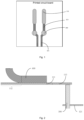
- a high-speed differential surface-mount device pad (111) needs to be connected to a differential through hole (300) by means of a differential microstrip line (113) on the surface layer, and the inner layer is fanned out by means of a differential strip line (121).
- the signal flow direction of the design is: high-speed differential surface-mount device pad (111) ⁇ differential microstrip line (113) ⁇ differential through hole (300) ⁇ differential strip line (121).
- the high-speed differential surface-mount device pad (111) needs to be longer than the tail end of the L-shaped welding pin (400) in the length direction.
- a branch structure of this portion forms a stub (112), which affects the impedance of the high-speed differential surface-mount device pad (111).
- a section of stub (112) is also left between the contact point of the gold finger pad (111) and the spring sheet (500) and the tail end of the pad, thereby affecting the impedance of the gold finger, as shown in Fig. 3 .
- the stub at the tail end of the surface-mounted device pad or the gold finger pad is coupled to the reference ground to form a capacitive impedance discontinuity
- the equivalent circuit thereof is shown in Fig. 4 , wherein C1 and C2 are equivalent capacitors of the pad stub; and the equivalent parts of structures such as welding pins and routing lines are as shown by labels. Due to the influence of C1 and C2, the differential signals (PP-IN and PN-IN) connected from the high-speed differential pad (111) are easily reflected, resulting in poor transmission quality of the high-speed signals. Therefore, how to reduce the capacitive coupling between the pad stub and the reference ground, i.e., the values of C1 and C2, to improve the transmission quality of high-speed signals, has become an urgent technical problem to be solved.
- Fig. 5 is a side view I of a printed circuit board with a pad according to the present invention.
- printed circuit board comprises: a signal layer 100 and a reference layer 200, wherein the signal layer 100 is provided with a pad 111, the pad 111 comprises a stub 112, the reference layer 200 is provided with a first anti-pad 221, the vertical projection of the stub 112 on the reference layer 200 is located in a coverage area of the first anti-pad 221, and the first anti-pad 221 is configured to reduce the impedance of the stub 112.
- the pad 111 may be a surface-mounted device pad, may also be a gold finger pad, and may also be other types of pads similar to the surface-mounted device pad or the gold finger pad, which is not specifically limited in the present invention. Whether the pad 111 is a surface-mounted device pad or a gold finger pad, the pad has a stub 112, and the principle is shown in Figs. 2 and 3 . For the sake of illustration, all subsequent embodiments use surface-mount device pads for schematic explanation.
- the signal layer 100 is configured to access and transmit a high-speed signal
- the reference layer 200 is configured to set a first anti-pad 221, so as to increase the distance between the stub 112 and the reference ground, reduce capacitive coupling and optimize impedance, and improve the signal transmission quality.
- the portion of the pad 111 exceeding the welding end a of the L-shaped welding pin 400 in a length direction forms the stub 112.
- the signal layer 100 may be provided with N pads 111, N being any integer greater than or equal to 1, and each pad 111 may be formed by two sub-pads and is configured to access a high-speed differential signal.
- each pad 111 exceeding the welding end a of the L-shaped welding pin 400 in the length direction forms a corresponding stub 112.
- the reference layer 200 may be provided with N first anti-pads 221, and the N first anti-pads 221 are in one-to-one correspondence with the N first pads 111, that is, the first anti-pad 221 is provided below the area of the stub 112 of each pad 111, so as to reduce impedance of the area of the stub 112 of each pad 111, thereby improving transmission quality of each high-speed signal.
- the signal layer 100 comprises a first sub-signal layer 110 and a second sub-signal layer 120;
- the reference layer 200 comprises a first sub-reference layer 210 and a second sub-reference layer 220;
- the first sub-signal layer 110, the first sub-reference layer 210, the second sub-reference layer 220 and the second sub-signal layer 120 are sequentially stacked;
- the first sub-signal layer 110, the first sub-reference layer 210, the second sub-reference layer 220 and the second sub-signal layer 120 are all provided with a through hole 300 penetrating each other;
- the first sub-signal layer 110 is provided with a pad 111 and a first signal wiring 113, and the pad 111 is connected to the first signal wiring 113;
- the second sub-signal layer 120 is provided with a second signal wiring 121, the first signal wiring 113 is connected to the second signal wiring 121 by means of a through hole 300, and the second signal wiring 121 is configured
- the signal layer 100 may include a first sub-signal layer 110 and a second sub-signal layer 120, and is configured to receive and transmit a signal; and the flow direction of the signal is: pad 111 ⁇ first signal wiring 113-via 300-second signal wiring 121.
- the reference layer 200 may comprise a first sub-reference layer 210 and a second sub-reference layer 220, and thus the overall impedance of the pad 111 can be reduced by using the second anti-pad 211 on the first sub-reference layer 210, and the impedance of the stub 112 can be reduced by using the first anti-pad 221 on the second sub-signal layer 120, thereby further improving the transmission quality of a signal.
- the arrangement manner of the first anti-pad 221 and the second anti-pad 211 is removing a metal material in a partial area of the reference layer made of the metal material, and replacing the metal material in the area with an insulating dielectric material.
- the first anti-pad 221 on the second sub-signal layer 120 can be used to reduce the impedance of the stub 112
- the vertical projection of the second anti-pad 211 on the second sub-reference layer 220 needs to include a coverage area of the first anti-pad 221, that is, the size of the second anti-pad 211 is greater than the size of the first anti-pad 221.
- Fig. 7 is a top-view overlay schematic diagram of a printed circuit board with a pad according to an embodiment of the present invention.
- the pad 111 includes a first sub-pad 1111 and a second sub-pad 1112;
- the first signal wiring 113 includes a first microstrip line 1131 and a second microstrip line 1132;
- the second signal wiring 121 includes a first strip line 1211 and a second strip line 1212;
- the first sub-pad 1111 is connected to the first microstrip line 1131;
- the first microstrip line 1131 is connected to the first strip line 1211 by means of a through hole 300;
- the first sub-pad 1111 comprises a first stub 1121;
- the second sub-pad 1112 is connected to the second microstrip line 1132;
- the second microstrip line 1132 is connected to the second strip line 1212 by means of a through hole 300;
- the second sub-pad 1112 includes a second stub 1122.
- the number of first anti-pads 221 is in one-to-one correspondence with the number of pads 111; and the first anti-pads 221 are used to optimize the impedance of the first stub 1121 on the first sub-pad 1111 among the pads 111 and the impedance of the second stub 1122 on the second sub-pad 1112 among the pads 111.
- the channel impedance of the high-speed differential signal may be optimized, and the influence of signal reflection on the high-speed differential signal may be reduced, thereby improving the integrity of the high-speed differential signal.
- both the vertical projection of the first sub-pad 1111 on the first sub-reference layer 210 and the vertical projection of the second sub-pad 1112 on the first sub-reference layer 210 are within the coverage area of the second counter-pad 211; the vertical projection of the first stub 1121 on the second sub-reference layer 220 and the vertical projection of the second stub 1122 on the second sub-reference layer 220 are both located within the coverage area of the first anti-pad 221.
- the second anti-pad 211 is added below the first sub-pad 1111 and the second sub-pad 1112 as the first reference layer 200 of the pad 111, and the size of the second anti-pad 211 may be determined by means of emulation.
- the second anti-pad 211 is added below the first sub-pad 1111 and the second sub-pad 1112, and an effect of reducing impedance of the first sub-pad 1111 and the second sub-pad 1112 can be achieved by reducing the capacitive coupling between the first sub-pad 1111 and second sub-pad 1112 and the reference ground.
- the first anti-pad 221 is added below the second anti-pad 211 as the second reference layer 200 of the pad 111.
- the size of the first anti-pad 221 may be determined by means of emulation.
- a first anti-pad 221 is added below the first stub 1121 and the second stub 1122, and an effect of reducing the impedances of the first stub 1121 and the second stub 1122 can be achieved by reducing the capacitive coupling between the first stub 1121 and second stub 1122 and the reference ground, thereby avoiding the occurrence of impedance low points, reducing impedance fluctuations, and increasing the channel bandwidth.
- the second anti-pad 211 can better optimize the impedances of the first sub-pad 1111 and the second sub-pad 1112, and the first anti-pad 221 can further optimize the impedances of the first stub 1121 and the second stub 1122, thereby improving signal transmission quality.
- both the first end of the vertical projection of the first stub 1121 and the first end of the vertical projection of the second stub 1122 are aligned with the first side edge of the coverage area of the first anti-pad 221; neither the second end of the vertical projection of the first stub 1121 nor the second end of the vertical projection of the second stub 1122 exceeds the second side edge of the coverage area of the first anti-pad 221; the first end of the vertical projection of the first stub 1121 is the end of the vertical projection of the first stub 1121 close to the through hole 300; the second end of the vertical projection of the first stub 1121 is the end opposite to the first end of the vertical projection of the first stub 1121; the first end of the vertical projection of the second stub 1122 is the end of the vertical projection of the second stub 1122 close to the through hole 300; the second end of the vertical projection of the second stub 1122 is the end opposite to the first end of
- the size and position of the first anti-pad 221 may be determined according to simulation; when both the first end of the vertical projection of the first stub 1121 and the first end of the vertical projection of the second stub 1122 are aligned with the first side edge of the coverage area of the first anti-pad 221, and when neither the second end of the vertical projection of the first stub 1121 nor the second end of the vertical projection of the second stub 1122 exceeds the second side edge of the coverage area of the first anti-pad 221, the impedance optimization of the first stub 1121 and the second stub 1122 is obvious.
- a ratio of a distance by which the second side edge of the coverage area of the first anti-pad 221 exceeds the second end of the vertical projection of the first stub 1121 to a length of the first stub 1121 is less than 1; and a ratio of a distance by which the second side edge of the coverage area of the first anti-pad 221 exceeds the second end of the vertical projection of the second stub 1122 to a length of the second stub 1122 is less than 1.
- a stub anti-pad i.e. the first anti-pad 221 hereinbefore
- the problem of impedance discontinuity at the tail end of the SMD pad can be effectively reduced, the impedance matching and signal integrity performance can be improved, and the channel return loss and insertion loss can be optimized.
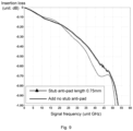
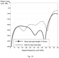
- Figs. 8 to 10 when the length of the stub 112 of the pad 111 is 0.5 mm, the influence of adding no stub anti-pad on the channel impedance and the influence of adding stub anti-pads of different lengths on the channel impedance are shown in Fig. 8 , wherein the horizontal coordinate in Fig.
- TDR Time Domain Reflectometry
- channel impedance a measurement value corresponding to each measurement time (i.e. channel impedance). It can be seen from figure 8 that the impedance continuity when no stub anti-pad is added is lower than the impedance continuity when a stub anti-pad is added; and as the length of the stub anti-pad increases, the channel impedance continuity gradually increases, and when the length of the stub anti-pad is 0.75 mm, the channel impedance continuity is optimal. Meanwhile, when the length of the stub anti-pad is 0.75 mm, the optimization effect of insertion loss and return-wave loss of the high-speed signal is also obvious, as shown in Figs. 9 and 10 .
- the horizontal coordinate in Fig. 9 represents a signal frequency
- the vertical coordinate represents an insertion loss corresponding to each signal frequency; when the signal frequency reaches a certain frequency value, an insertion loss when a stub anti-pad is added is higher than an insertion loss when no stub anti-pad is added.
- the horizontal coordinate in Fig. 10 represents a signal frequency, and the vertical coordinate represents a return loss corresponding to each signal frequency; when the signal frequency reaches a certain frequency value, a return loss when a stub anti-pad is added is lower than a return loss when no stub anti-pad is added.
- the present invention achieves an innovative improvement in technical value, and achieves both signal integrity and design reliability from the perspective of the design of anti-pads on the inner layer of the printed circuit board, thereby solving the signal distortion problem caused by the fact that pad stub impedance in the prior art cannot be optimized.
- the length of the stub anti-pad is not as long as possible, when the length of the stub anti-pad exceeds twice the length of the stub 112, it will lead to a decrease in impedance continuity. Therefore, when setting the length of the stub anti-pad, the distance by which the stub anti-pad exceeds the stub 112 is usually less than one times the length of the stub 112.
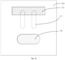
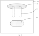
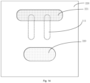
- the schematic diagram of the fan-out structure of the first sub-reference layer 210 of the pad 111 is shown in Fig. 11
- the schematic diagram of the fan-out structure of the second sub-reference layer 220 of the pad 111 is shown in Fig. 12 .
- the shape of the coverage area of the first anti-pad 221 is any one of rectangle, ellipse and a racetrack shape.
- the shape of the coverage area of the first anti-pad 221 may be any regular shape or irregular shape.
- the shape of a coverage area of the first anti-pad 221 may be rectangle, ellipse, a racetrack shape, or the like.
- the shape of the coverage area of the first anti-pad 221 may be rectangle, and may also be ellipse or a racetrack shape, as shown in Figs. 13 and 14 . That is to say, the same effect can be achieved by replacing the rectangular first anti-pad 221 in Fig. 12 with the oval first anti-pad 221 or the first anti-pad 221 in a racetrack shape.
- the first sub-reference layer 210 is further provided with a third anti-pad 310
- the second sub-reference layer 220 is further provided with a fourth anti-pad 320
- the third anti-pad 310 and the fourth anti-pad 320 are both configured to reduce the impedance of the through hole 300. In this way, the transmission quality of the high-speed signal can be further improved.
- both the first sub-reference layer 210 and the second sub-reference layer 220 are metal layers connected to the ground terminal.
- the first anti-pad 221 and the second anti-pad 211 be provided on the metal layer connected to the ground terminal, but they can also serve as a reference ground of the pad 111, thereby achieving impedance optimization of the pad and the pad stub 112.
- a design method for a printed circuit board having a pad according to the present invention is as follows.
- the entire impedance fluctuation of the channel can be reduced by using the pad stub anti-pad, and this not only eliminates the need to change the pad size or perform pad trimming, but also optimizes the impedance fluctuation of the SMD while ensuring reliable welding, and can also reduce the reflection of high-speed signals and improve signal integrity.
- the present invention further provides a communication device comprising the printed circuit board according to any one of the above embodiments.
- the communication device may be a printed circuit board including a surface-mounted device pad or a gold finger pad, and is suitable for a wired communication device and a wireless communication device of 112 Gbps or more.
- the present invention provides a printed circuit board having a pad and a communication device, so as to solve the problem, in some cases, of poor transmission quality of a high-speed signal due to the fact that the stub at the tail end of the surface-mounted device pad or the gold finger pad is coupled to the reference ground to form a capacitive impedance discontinuity.
- the printed circuit board includes a signal layer and a reference layer.
- the signal layer is provided with a pad, and the pad comprises a stub;
- the reference layer is provided with a first anti-pad, the vertical projection of the stub in the reference layer is located in a coverage area of the first anti-pad, and the first anti-pad is used for reducing the impedance of the stub.
- a first anti-pad may be provided below a stub area of a pad, and capacitive coupling between the stub and the reference ground is reduced using the first anti-pad, thereby improving the transmission quality of the high-speed signal.
Landscapes
- Engineering & Computer Science (AREA)
- Microelectronics & Electronic Packaging (AREA)
- Structure Of Printed Boards (AREA)
- Production Of Multi-Layered Print Wiring Board (AREA)
Applications Claiming Priority (2)
| Application Number | Priority Date | Filing Date | Title |
|---|---|---|---|
| CN202211042562.3A CN117440593A (zh) | 2022-08-29 | 2022-08-29 | 具有焊盘的印制电路板及通信设备 |
| PCT/CN2023/083177 WO2024045574A1 (zh) | 2022-08-29 | 2023-03-22 | 具有焊盘的印制电路板及通信设备 |
Publications (2)
| Publication Number | Publication Date |
|---|---|
| EP4568427A1 true EP4568427A1 (de) | 2025-06-11 |
| EP4568427A4 EP4568427A4 (de) | 2025-12-24 |
Family
ID=89557146
Family Applications (1)
| Application Number | Title | Priority Date | Filing Date |
|---|---|---|---|
| EP23858616.8A Pending EP4568427A4 (de) | 2022-08-29 | 2023-03-22 | Leiterplatte mit einem pad und kommunikationsvorrichtung |
Country Status (5)
| Country | Link |
|---|---|
| US (1) | US20260068034A1 (de) |
| EP (1) | EP4568427A4 (de) |
| JP (1) | JP7836465B2 (de) |
| CN (1) | CN117440593A (de) |
| WO (1) | WO2024045574A1 (de) |
Families Citing this family (1)
| Publication number | Priority date | Publication date | Assignee | Title |
|---|---|---|---|---|
| CN118215212A (zh) * | 2024-05-22 | 2024-06-18 | 苏州元脑智能科技有限公司 | 差分焊盘单元、印刷线路板、光模块电路板、交换机及计算机网络 |
Family Cites Families (12)
| Publication number | Priority date | Publication date | Assignee | Title |
|---|---|---|---|---|
| CN1305354C (zh) | 2001-10-10 | 2007-03-14 | 莫莱克斯公司 | 高速差分信号边缘卡连接器电路板布局 |
| US6803527B2 (en) * | 2002-03-26 | 2004-10-12 | Intel Corporation | Circuit board with via through surface mount device contact |
| JP4834385B2 (ja) | 2005-11-22 | 2011-12-14 | 株式会社日立製作所 | プリント基板および電子装置 |
| JP5003359B2 (ja) | 2007-08-31 | 2012-08-15 | 日本電気株式会社 | プリント配線基板 |
| US9380704B2 (en) * | 2011-03-30 | 2016-06-28 | Nec Corporation | Transmission system and method for constructing backplane system |
| JP5922604B2 (ja) | 2013-03-05 | 2016-05-24 | 日本電信電話株式会社 | 多層配線基板 |
| US10410984B1 (en) * | 2015-06-02 | 2019-09-10 | Sarcina Technology LLC | Package substrate differential impedance optimization for 25 to 60 GBPS and beyond |
| CN106793455B (zh) * | 2016-12-14 | 2019-06-14 | 广东海信宽带科技有限公司 | 一种光模块 |
| CN106646777B (zh) * | 2016-12-14 | 2019-05-28 | 青岛海信宽带多媒体技术有限公司 | 一种光模块及其设计方法 |
| CN108012415A (zh) * | 2017-11-17 | 2018-05-08 | 新华三技术有限公司 | 表贴焊盘结构、印制电路板及其制备工艺 |
| CN108901126B (zh) * | 2018-08-23 | 2019-09-13 | 新华三信息技术有限公司 | 印制电路板、电子设备及印制电路板的生产工艺 |
| US10791629B1 (en) * | 2019-09-06 | 2020-09-29 | Cisco Technology, Inc. | Printed circuit board configuration to facilitate a surface mount double density QSFP connector footprint in a belly-to-belly alignment |
-
2022
- 2022-08-29 CN CN202211042562.3A patent/CN117440593A/zh active Pending
-
2023
- 2023-03-22 WO PCT/CN2023/083177 patent/WO2024045574A1/zh not_active Ceased
- 2023-03-22 US US19/106,262 patent/US20260068034A1/en active Pending
- 2023-03-22 JP JP2025511372A patent/JP7836465B2/ja active Active
- 2023-03-22 EP EP23858616.8A patent/EP4568427A4/de active Pending
Also Published As
| Publication number | Publication date |
|---|---|
| WO2024045574A1 (zh) | 2024-03-07 |
| CN117440593A (zh) | 2024-01-23 |
| US20260068034A1 (en) | 2026-03-05 |
| JP7836465B2 (ja) | 2026-03-26 |
| EP4568427A4 (de) | 2025-12-24 |
| JP2025526970A (ja) | 2025-08-15 |
Similar Documents
| Publication | Publication Date | Title |
|---|---|---|
| US7564695B2 (en) | Circuit connection structure and printed circuit board | |
| WO2012099837A1 (en) | Substrate and electronic component including same | |
| US20160088724A1 (en) | Grounding pattern structure for high-frequency connection pad of circuit board | |
| EP4568427A1 (de) | Leiterplatte mit einem pad und kommunikationsvorrichtung | |
| US8384489B2 (en) | Serpentine micro-strip lines configured in an aggressor/victim type transmission line structure | |
| US20040016569A1 (en) | Add-in card edge-finger design/stackup to optimize connector performance | |
| JP6441850B2 (ja) | 多層プリント配線板 | |
| US8227707B2 (en) | Coaxial connector mounted circuit board | |
| EP1568099B1 (de) | Eine schaltung, die ein differenzsignal abgreift | |
| CN108811315B (zh) | 金手指结构 | |
| CN113473724B (zh) | 印刷电路板和印刷电路板布线方法 | |
| CN214154943U (zh) | 印刷电路板和视频处理设备 | |
| CN116056323A (zh) | 印刷电路板及电子设备 | |
| JP2016207834A (ja) | 印刷配線板 | |
| CN114585146B (zh) | 用于提升隔离度的电路板结构 | |
| US20250280493A1 (en) | Vertical conductive structure transition impedance optimization | |
| CN215420912U (zh) | 一种满足六类传输性能的线路板结构 | |
| CN223694063U (zh) | 一种改善表贴焊盘阻抗的非金属化孔的pcb结构 | |
| CN222030125U (zh) | Pcie信号板及pcie板卡 | |
| CN220292254U (zh) | 一种改善阻抗的pcie金手指结构 | |
| CN115473062B (zh) | 一种高速信号传输板卡及电子设备 | |
| US10999929B2 (en) | Expansion card interfaces for high-frequency signals and methods of making the same | |
| WO2025030933A1 (zh) | 电路板及其制备方法和电子设备 | |
| CN117715296A (zh) | 一种印刷电路板和电子设备 | |
| KR100372010B1 (ko) | 인쇄기판회로 패턴을 이용한 인핸스드 카테고리 5급모듈라 잭 |
Legal Events
| Date | Code | Title | Description |
|---|---|---|---|
| STAA | Information on the status of an ep patent application or granted ep patent |
Free format text: STATUS: THE INTERNATIONAL PUBLICATION HAS BEEN MADE |
|
| PUAI | Public reference made under article 153(3) epc to a published international application that has entered the european phase |
Free format text: ORIGINAL CODE: 0009012 |
|
| STAA | Information on the status of an ep patent application or granted ep patent |
Free format text: STATUS: REQUEST FOR EXAMINATION WAS MADE |
|
| 17P | Request for examination filed |
Effective date: 20250306 |
|
| AK | Designated contracting states |
Kind code of ref document: A1 Designated state(s): AL AT BE BG CH CY CZ DE DK EE ES FI FR GB GR HR HU IE IS IT LI LT LU LV MC ME MK MT NL NO PL PT RO RS SE SI SK SM TR |
|
| DAV | Request for validation of the european patent (deleted) | ||
| DAX | Request for extension of the european patent (deleted) | ||
| A4 | Supplementary search report drawn up and despatched |
Effective date: 20251120 |
|
| RIC1 | Information provided on ipc code assigned before grant |
Ipc: H05K 1/02 20060101AFI20251114BHEP Ipc: H05K 1/11 20060101ALN20251114BHEP Ipc: H05K 3/34 20060101ALN20251114BHEP Ipc: H05K 3/42 20060101ALN20251114BHEP |