EP4568264A1 - Optical assembly, preparation method for optical assembly, and electronic device - Google Patents
Optical assembly, preparation method for optical assembly, and electronic device Download PDFInfo
- Publication number
- EP4568264A1 EP4568264A1 EP23870294.8A EP23870294A EP4568264A1 EP 4568264 A1 EP4568264 A1 EP 4568264A1 EP 23870294 A EP23870294 A EP 23870294A EP 4568264 A1 EP4568264 A1 EP 4568264A1
- Authority
- EP
- European Patent Office
- Prior art keywords
- optical
- layer
- micro
- hydrophobic
- light
- Prior art date
- Legal status (The legal status is an assumption and is not a legal conclusion. Google has not performed a legal analysis and makes no representation as to the accuracy of the status listed.)
- Pending
Links
Images




Classifications
-
- G—PHYSICS
- G02—OPTICS
- G02B—OPTICAL ELEMENTS, SYSTEMS OR APPARATUS
- G02B1/00—Optical elements characterised by the material of which they are made; Optical coatings for optical elements
- G02B1/10—Optical coatings produced by application to, or surface treatment of, optical elements
- G02B1/18—Coatings for keeping optical surfaces clean, e.g. hydrophobic or photo-catalytic films
-
- G—PHYSICS
- G02—OPTICS
- G02B—OPTICAL ELEMENTS, SYSTEMS OR APPARATUS
- G02B1/00—Optical elements characterised by the material of which they are made; Optical coatings for optical elements
- G02B1/10—Optical coatings produced by application to, or surface treatment of, optical elements
- G02B1/11—Anti-reflection coatings
-
- G—PHYSICS
- G02—OPTICS
- G02B—OPTICAL ELEMENTS, SYSTEMS OR APPARATUS
- G02B1/00—Optical elements characterised by the material of which they are made; Optical coatings for optical elements
- G02B1/10—Optical coatings produced by application to, or surface treatment of, optical elements
- G02B1/11—Anti-reflection coatings
- G02B1/113—Anti-reflection coatings using inorganic layer materials only
-
- G—PHYSICS
- G02—OPTICS
- G02B—OPTICAL ELEMENTS, SYSTEMS OR APPARATUS
- G02B27/00—Optical systems or apparatus not provided for by any of the groups G02B1/00 - G02B26/00, G02B30/00
- G02B27/0018—Optical systems or apparatus not provided for by any of the groups G02B1/00 - G02B26/00, G02B30/00 with means for preventing ghost images
-
- H—ELECTRICITY
- H04—ELECTRIC COMMUNICATION TECHNIQUE
- H04N—PICTORIAL COMMUNICATION, e.g. TELEVISION
- H04N23/00—Cameras or camera modules comprising electronic image sensors; Control thereof
- H04N23/50—Constructional details
- H04N23/52—Elements optimising image sensor operation, e.g. for electromagnetic interference [EMI] protection or temperature control by heat transfer or cooling elements
-
- H—ELECTRICITY
- H04—ELECTRIC COMMUNICATION TECHNIQUE
- H04N—PICTORIAL COMMUNICATION, e.g. TELEVISION
- H04N23/00—Cameras or camera modules comprising electronic image sensors; Control thereof
- H04N23/50—Constructional details
- H04N23/55—Optical parts specially adapted for electronic image sensors; Mounting thereof
-
- G—PHYSICS
- G02—OPTICS
- G02B—OPTICAL ELEMENTS, SYSTEMS OR APPARATUS
- G02B1/00—Optical elements characterised by the material of which they are made; Optical coatings for optical elements
- G02B1/10—Optical coatings produced by application to, or surface treatment of, optical elements
- G02B1/11—Anti-reflection coatings
- G02B1/118—Anti-reflection coatings having sub-optical wavelength surface structures designed to provide an enhanced transmittance, e.g. moth-eye structures
-
- G—PHYSICS
- G02—OPTICS
- G02B—OPTICAL ELEMENTS, SYSTEMS OR APPARATUS
- G02B2207/00—Coding scheme for general features or characteristics of optical elements and systems of subclass G02B, but not including elements and systems which would be classified in G02B6/00 and subgroups
- G02B2207/101—Nanooptics
-
- G—PHYSICS
- G02—OPTICS
- G02B—OPTICAL ELEMENTS, SYSTEMS OR APPARATUS
- G02B27/00—Optical systems or apparatus not provided for by any of the groups G02B1/00 - G02B26/00, G02B30/00
- G02B27/0006—Optical systems or apparatus not provided for by any of the groups G02B1/00 - G02B26/00, G02B30/00 with means to keep optical surfaces clean, e.g. by preventing or removing dirt, stains, contamination, condensation
Definitions
- This application relates to the field of electronic device technologies, and in particular, to an optical assembly, an optical assembly preparation method, and an electronic device.
- a camera module has become a necessary functional module in an electronic device such as a mobile phone, a tablet computer, a notebook computer, or a wearable device. With continuous development of electronic devices, people's requirements on the photographing effect of the camera module gradually increase.
- the optical cover plate further includes a hydrophobic film layer.
- the hydrophobic film layer is light-transmissive, is located on a side of the optical body layer facing the optical component, and covers the light-transmissive area.
- a surface of the hydrophobic film layer facing the optical component is a hydrophobic rough surface with a first micro-nano structure.
- the first anti-reflection layer through arrangement of the first anti-reflection layer, a reflectance of the inner surface of the optical cover plate can be reduced, and ghosting intensity during photographing in a general scenario and in a strong contrast environment can be reduced.
- formation of the first micro-nano structure can be facilitated due to existence of the second micro-nano structure.
- a surface of the underlayer facing the hydrophobic layer of the hydrophobic film layer has a third micro-nano structure, where the third micro-nano structure covers the second micro-nano structure in the optical body layer and is adhered between the second micro-nano structure and the first micro-nano structure; and a shape of the third micro-nano structure matches the shape of the second micro-nano structure.
- the base material of the first anti-reflection layer is silicon dioxide
- the active underlayer is a silicon dioxide layer.
- the hydrophobic layer in the hydrophobic film layer is a perfluoropolyethers plating layer, so that while it is satisfied that the hydrophobic rough surface of the hydrophobic layer has good hydrophobic and oleophobic properties, light transmission efficiency in the light-transmissive area is not affected.
- a water drop angle of the optical cover plate on the hydrophobic film layer is greater than 150°, and/or a roll angle of the optical cover plate on the hydrophobic film layer is less than 40°. In this way, the optical cover plate has good hydrophobic performance on the hydrophobic film layer (namely, the light-transmissive area).
- the optical body layer further includes a second anti-reflection layer, where the second anti-reflection layer is light-transmissive and is located on a surface of the substrate of the optical body layer facing away from the hydrophobic film layer, to reduce reflection of light by an outer surface of the optical cover plate and protect the outer surface of the optical cover plate from being scratched.
- the second anti-reflection layer is light-transmissive and is located on a surface of the substrate of the optical body layer facing away from the hydrophobic film layer, to reduce reflection of light by an outer surface of the optical cover plate and protect the outer surface of the optical cover plate from being scratched.
- a second aspect of embodiments of this application further provides an optical assembly preparation method.
- the preparation method is used for manufacturing the optical assembly according to any one of the foregoing implementations.
- the preparation method includes:
- the surface of the optical stack on which the hydrophobic rough surface is arranged can have hydrophobic performance in the light-transmissive area. Because the hydrophobic rough surface is arranged facing the optical component, the surface of the optical stack on which the hydrophobic rough surface is arranged can be used as an inner surface of the optical cover plate, and the light-transmissive area of the optical stack can be used as a light-transmissive area of the optical cover plate, so that when the optical cover plate and the optical component are combined to form the optical assembly, a water drop angle of the inner surface of the optical cover plate in the light-transmissive area can be increased, thereby effectively reducing the proportion of mist-like dirt occurring on the optical cover plate after the entire electronic device is plated.
- the preparing the optical stack specifically includes:
- the first anti-reflection layer due to existence of the second micro-nano structure on the first anti-reflection layer, it is facilitate to formation of the first micro-nano structure on the hydrophobic film layer, to reduce the proportion of mist-like dirt occurring on the optical cover plate in the light-transmissive area, and a reflectance of the surface of the hydrophobic film layer can be reduced, to reduce ghosting intensity during photographing in a general scenario and in a strong contrast environment.
- the forming the hydrophobic film layer on the surface of the optical stack specifically includes:
- the surface of the hydrophobic layer facing the optical component can form a hydrophobic rough surface, to be combined with the first micro-nano structure, increase a water drop angle of the substrate in the light-transmissive area, and reduce the proportion of mist-like dirt formed in the light-transmissive area.
- processing the surface of the to-be-processed plate to form the optical stack specifically includes:
- the surface of the to-be-processed plate can be selectively etched, to form the second micro-nano structure.
- processing the surface of the to-be-processed plate to form the optical stack specifically includes:
- the manufacturing process and a structure of the first anti-reflection layer can be more diversified.
- the preparation method further includes: forming a second anti-reflection layer on a surface of the optical stack facing away from the hydrophobic film layer, where the optical body layer further includes the second anti-reflection layer.
- a reflectance of the surface (which is an outer surface of the optical cover plate) of the optical body layer facing away from the hydrophobic film layer can be reduced to less than 0.3%, thereby effectively preventing ghosting from being generated during photographing by the electronic device in a general scenario and a strong contrast scenario.
- a third aspect of embodiments of this application further provides an electronic device.
- the electronic device includes a housing and the optical assembly according to any one of the foregoing implementations.
- An optical component in the optical assembly is located in an accommodating space of the housing, and an optical cover plate is located on the housing and covers a light-incident surface of the optical component.
- Water drop angle is also referred to as a water contact angle, which is a type of a contact angle, and is usually defined as an angle between a gas phase-liquid phase 300 interface and a solid phase 200-liquid phase 300 interface at an intersection between the solid phase 200, the liquid phase 300, and the gas phase (not marked in FIG. 1 ).
- an angle a illustrates a water drop angle.
- the water drop angle may be used for measuring mutual wettability of the solid phase 200 and the liquid phase 300 and exhibited hydrophilic performance or hydrophobic performance.
- a small (for example, less than 90°) water drop angle indicates that a surface (the hydrophilic performance) of the solid phase 200 has high humidity and low exhibited energy, and is easy to be pasted.
- a large water drop angle indicates that the surface of the solid phase 200 exhibits the hydrophobic performance and has poor surface adhesion.
- a material with a water drop angle exceeds 150° is referred to as a super-hydrophobic material.
- the water drop angle may further be used as a measure of an anti-fouling (for example, anti-fingerprint) effect of the solid phase 200. To achieve the anti-fingerprint effect, the water drop angle is generally required to be greater than 120°.
- Contact angle of n-hexadecane is also referred to as an oil contact angle (or an oil drop angle).
- the oil drop angle is similar to the water drop angle, and is also a type of the contact angle.
- the oil drop angle is less than 90°, it indicates that the surface of the solid phase 200 has high oleophilic performance.
- the oil drop angle is greater than or equal to 90°, it indicates that the surface of the solid phase 200 has high oleophobic performance, and the adhesion of an oil drop on the surface of the solid phase 200 is poor.
- the water drop angle generally represents performance of a water drop on a horizontal plane, however, a plane in reality is more of an inclined plane.
- a liquid for example, a water drop
- Micro-nano structure may be understood as that a material surface has a micro-sized and/or nano-sized surface structure.
- the micro-nano structure is a morphology of a micro structure of the material surface.
- the electronic device may include, but is not limited to, electronic devices such as a mobile phone, a tablet computer (namely, a pad), a virtual reality (virtual reality, VR) device, a notebook computer, a personal computer (personal computer, PC), an ultra-mobile personal computer (ultra-mobile personal computer, UMPC), a handheld computer, a smart wearable device, and a point of sales (point of sales, POS).
- electronic devices such as a mobile phone, a tablet computer (namely, a pad), a virtual reality (virtual reality, VR) device, a notebook computer, a personal computer (personal computer, PC), an ultra-mobile personal computer (ultra-mobile personal computer, UMPC), a handheld computer, a smart wearable device, and a point of sales (point of sales, POS).
- electronic devices such as a mobile phone, a tablet computer (namely, a pad), a virtual reality (virtual reality, VR) device, a notebook computer, a personal computer (personal computer, PC), an ultra-
- the middle frame 21 includes a middle plate 212 and a side frame 211 that are connected.
- the side frame 211 surrounds a peripheral edge of the middle plate 212, and forms the middle frame 21 with the middle plate 212.
- the side frame 211 is a square-ring structure formed by a plurality of side frames 211 connected head-to-tail.
- the electronic device 100 when the electronic device 100 has a display function, the electronic device 100 further includes a display screen 1.
- the display screen 1 is mounted on a side of the side frame 211 that is opposite to the rear cover 22.
- the rear cover 22 covers a side of the middle frame 21, and encloses, jointly with the middle frame 21 and the rear cover 22, an accommodating space (not shown in the figure) of the electronic device 100.
- Structural members of the electronic device 100 such as a mainboard 6, a battery 5, a microphone, a speaker, and an earphone may be arranged in the accommodating space.
- the mainboard 6 and the battery 5 may be arranged together on a side of the middle plate 212 facing the rear cover 22, to facilitate electrical connection between the mainboard 6 and the battery 5.
- the mainboard 6 may be understood as a printed mainboard 6 bearing electronic elements.
- the electronic elements in the mainboard may include, but are not limited to, a system on a chip (system on a chip, SoC), an antenna module, a Bluetooth module, a wireless communication module (such as a Wi-Fi module), a positioning module, a radio frequency (radio frequency, RF) chip, a radio frequency power amplifier (radio frequency poZer amplifier, RFPA), a storage module (for example, a double data rate (double data rate, DDR) memory), a power management module, a charging module, a screen display and operation module, and the like.
- SoC system on a chip
- SoC system on a chip
- SoC system on a chip
- SoC system on a chip
- RF radio frequency
- RFPA radio frequency poZer amplifier
- storage module for example, a double data rate (double data rate, DDR) memory
- power management module for example, a charging module, a screen display and operation module, and the like.
- a surface on which the display screen 1 is located constitutes a front face of the electronic device 100, and a surface on which the rear cover 22 is located constitutes a rear face of the electronic device 100.
- the display screen 1 is electrically connected to the mainboard 6, so that the display screen 1 can implement a display or operation function.
- the electronic device 100 further includes a camera module 3.
- the camera module 3 may be arranged in the accommodating space, and is electrically connected to the mainboard 6, so that when a user inputs a photographing instruction, the camera module 3 can be controlled through the mainboard 6 to photograph an image.
- FIG. 4 shows that a camera module 3 is arranged in the electronic device 100.
- a quantity of camera modules 3 is not limited to one, and the quantity of the camera modules 3 may be two or more.
- a plurality of (for example, three, four, or five) camera modules 3 are generally arranged in the electronic device 100. Some camera modules 3 may be arranged on a side of the middle frame 21 facing the display screen 1, to form front camera modules.
- FIG. 3 shows that the front camera module (not marked in the figure) is arranged in an area of the middle frame 21 toward a top and close to an edge of the electronic device 100. It may be understood that a position of the camera module 3 is not limited to the position shown in FIG. 3 , and may alternatively be located at another position of the electronic device 100.
- Some camera modules 3 may further be arranged on a side of the middle frame 21 facing the rear cover 22, to form a rear camera module (not marked in the figure).
- a rear camera module not marked in the figure. The following further describes a structure of the electronic device 100 by using a rear camera module as an example.
- the rear camera module may be arranged in an area of the middle frame 21 toward the top of the electronic device 100 and close to the edge.
- the rear camera modules may be randomly arranged in an X-Y plane of the electronic device 100.
- the plurality of rear camera modules may be arranged in an X direction, or the plurality of rear camera modules may be arranged in a Y direction.
- the X-Y plane may be understood as a plane formed by the X direction and the Y direction, and the plane is parallel to a display surface (not marked in the figure) of the display screen 1.
- the rear camera module may include, but is not limited to, an auto focus (Auto Focus, AF) module, a fix focus (Fix Focus, FF) module, a wide-angle camera module, a telephoto camera module, a color camera module, or a grayscale camera module.
- the telephoto camera module may include, but is not limited to, a periscope telephoto camera module (or a periscope camera module).
- the electronic device 100 may include any one of the foregoing camera modules 3, or include two or more of the foregoing camera modules 3.
- FIG. 5 is a schematic diagram of a structure of a rear face of an electronic device
- FIG. 6 is a schematic diagram of a structure of an optical cover plate on a rear face of the electronic device
- FIG. 7 is a cross-sectional view of the electronic device in FIG. 6 in a direction A-A.
- the electronic device 100 further includes an optical cover plate 4a.
- An opening 221 matching a structure of the optical cover plate 4a is arranged at a position on the rear cover 22 opposite to the camera module 3.
- the optical cover plate 4a is arranged at the opening 221 and covers the plurality of camera modules 3, to shield the camera modules 3 and protect the camera modules 3.
- the optical cover plate 4 may also be referred to as a lens cover plate.
- the camera module 3 may include a module body 31 and a lens 32.
- the module body 31 includes a driving apparatus 311.
- One part of the lens 32 is mounted in the driving apparatus 311, and the other part is exposed to the outside of the driving apparatus 311.
- the lens 32 usually includes one or a plurality of stacked lenses (for example, an optical lens).
- the driving apparatus 311 is configured to drive the lens 32 to move.
- the driving apparatus 311 may further drive the lens 32 to move toward the rear cover 22 or away from the rear cover 22 in a direction of an optical axis, to implement a zoom or focus function of the camera module 3.
- the periscope camera module may provide an optical zoom of 5 times, 10 times, or another times.
- the driving apparatus 311 may drive the lens 32 to move (for example, translate or rotate) in a plane in which the driving apparatus 311 is located, to compensate for hand wobbling of the user during photographing, to achieve an anti-wobble function of the camera module 3.
- the optical cover plate 4a may cover a light-incident surface 321 of the lens 32, and a light-transmissive area 414a is arranged on the optical cover plate 4a and a position of the camera module 3 covered by the optical cover plate 4a, so that light outside the electronic device 100 can pass through the light-transmissive area 414a and enter the lens 32, to achieve a photographing function of the camera module 3.
- the light-transmissive area 414a may also be referred to as a camera aperture area.
- a shape of the light-transmissive area 414a matches a shape of the lens 32. Generally, to increase a light entering amount of the lens 32, the shape of the light-transmissive area 414a may be larger than the shape of the lens 32.
- the optical cover plate 4a may further include a non-light-transmissive area 415a, and the non-light-transmissive area 415a surrounds a peripheral edge of the light-transmissive area 414a.
- the non-light-transmissive area 415a includes a shielding area 4152a and an adhering area 4151a, and the adhering area 4151a is arranged on the peripheral edge of the light-transmissive area 414a.
- the shielding area 4152a surrounds a side of the adhering area 4151a away from the light-transmissive area 414a.
- the driving apparatus 311 may be adhered to the adhering area 4151a (not shown in the figure) on an inner surface of the optical cover plate 4a by using a buffer adhesive such as a foam adhesive, to fix the camera module 3 to the optical cover plate 4a and the rear cover 22.
- a buffer adhesive such as a foam adhesive
- the adhering areas 4151a corresponding to the plurality of camera modules 3 may be connected through the adhering area 4151a, to form the non-light-transmissive area 415a.
- the inner surface of the optical cover plate 4a may be understood as a surface of the optical cover plate 4a facing the camera module 3, and an outer surface of the optical cover plate 4a may be understood as a surface of the optical cover plate 4a facing away from the camera module 3.
- the module body 31 further includes an optical filtering assembly 312 and an image sensor assembly 313.
- the optical filtering assembly 312 and the image sensor assembly 313 are sequentially arranged on a light exit side of the lens 32.
- the optical filtering assembly 312 may include an optical filter
- the image sensor assembly 313 may include an image sensor electrically connected to the mainboard. In this way, light outside the electronic device 100 enters the lens 32 through the light-transmissive area 414a, and exits through the lens 32. The light may sequentially pass through the optical filtering assembly 312 and the image sensor assembly 313, and is processed by the image sensor, to form an image, thereby achieving the photographing function of the camera module 3.
- the optical cover plate 4a includes a substrate 411a.
- the substrate 411a is used as the only light-transmissive optical element in the optical cover plate 4a, and is usually glass.
- the glass may include, but is not limited to, common glass, tempered glass, and the like.
- the common glass may be understood as an undecorated glass having a smooth surface.
- the tempered glass is a chemical strengthened glass obtained through chemical strengthening processing such as ion exchange performed on common glass. Both the light-transmissive area 414a and the non-light-transmissive area 415a are arranged on an optical body layer of the substrate.
- a surface (for example, an inner surface) of an existing optical cover plate 4a generally has a smooth planar structure, when a liquid, for example, a water drop, falls onto the inner surface of the optical cover plate 4a, the liquid may press against the optical cover plate 4a under an action of a weight of the liquid, so that the water drop is flattened, to attach to the optical cover plate 4a.
- FIG. 8 is a schematic diagram of a structure of one of the light-transmissive areas 414a of the optical cover plate 4a after the entire electronic device 100 is plated in the related art. Refer to FIG. 8 . After the entire electronic device is plated, the applicant finds that there is mist-like dirt 43 in the light-transmissive area 414a on the inner surface of the optical cover plate 4a corresponding to the camera module 3.
- the lens 32 is fixed behind the optical cover plate 4, and there is a spacing between the lens 32 and the optical cover plate 4a.
- air inside the electronic device 100 is extracted, and air between the lens 32 and the optical cover plate 4a is also extracted.
- atoms and molecules of a plating layer, moisture, and some small molecules of the foam adhesive attach to and aggregate on the inner surface of the optical cover plate 4a along with water drops in airflow during vacuum breaking.
- a spacing between the periscope camera module and the optical cover plate 4a is larger than a spacing between a lens 32 of another rear camera module and the optical cover plate 4a. Consequently, after the entire electronic device is plated, mist-like dirt 43 at a position on the optical cover plate 4a opposite to the periscope camera module is worse.
- an embodiment of this application provides an optical assembly, so that an original optical cover plate 4a of the electronic device 100 is replaced with an optical cover plate in the optical assembly, to cover a light-incident surface of an optical component, thereby effectively reducing a proportion of mist-like dirt occurring on the optical cover plate after the entire electronic device 100 is plated.
- FIG. 9 is a schematic diagram of a structure of an optical cover plate according to an embodiment of this application.
- FIG. 10 is a schematic exploded view of a part of a camera module in the optical cover plate in FIG. 9 in a light-transmissive area, to facilitate observation of a layered structure in an optical cover plate 4.
- a surface of the hydrophobic film layer 42 facing away from the optical component can be understood as an outer surface of the hydrophobic film layer 42.
- the light-transmissive area 414 of the optical body layer 41 may also be understood as a light-transmissive area 414 of the optical cover plate 4.
- the inner surface of the hydrophobic film layer 42 has hydrophobic performance, so that the wettability between the hydrophobic rough surface and the liquid phase 300 is low, and adhesion of a liquid (for example, a water drop) on the hydrophobic rough surface is poor, avoiding the atoms and molecules of the plating layer and some small molecules of the foam adhesive attaching to and aggregating on the hydrophobic rough surface along with a liquid (such as an oil drop or a water drop in airflow) after the entire electronic device 100 is plated, to reduce a proportion of mist-like dirt 43 occurring in the light-transmissive area 414 of the surface of the optical cover plate 4 facing the optical component (the inner surface of the optical cover plate).
- a liquid for example, a water drop
- the hydrophobic rough surface presents a rough morphology with a micro-sized and/or nano-sized surface structure, and an undulating micro-nano structure is formed on the hydrophobic rough surface.
- the hydrophobic rough surface has low surface energy, and surface tension between the air and the liquid is large, when the atoms and molecules of the plating layer and some small molecules of the foam adhesive attach to a liquid (such as an oil drop or a water drop in airflow) and fall on the first micro-nano structure 4211 along with the liquid, the liquid aggregates into a liquid drop and stands on the first micro-nano structure 4211, so that the liquid drop (for example, a water drop) has a large water drop angle on the hydrophobic rough surface.
- a liquid such as an oil drop or a water drop in airflow
- the liquid such as a water drop or an oil drop can have an extremely small roll angle on the hydrophobic rough surface, making it easier for the liquid aggregating on the hydrophobic rough surface to slide out of the light-transmissive area 414, to further reduce the proportion of mist-like dirt 43 on the light-transmissive area 414 on the inner surface of the optical cover plate 4 corresponding to the camera module 3 (such as the periscope camera module 3).
- the optical component may be the camera module 3, and the camera module 3 includes the lens 32.
- the optical body layer 41 blocks the light-incident surface 321 of the lens 32.
- the light-transmissive area 414 is opposite to a position of the lens 32, to protect the lens 32 by blocking the light-incident surface 321 of the lens 32 by using the optical cover plate 4, and further reduce the proportion of mist-like dirt 43 occurring on the inner surface of the optical cover plate 4 in the light-transmissive area 414.
- the optical body layer 41 may be located at the opening 221 of the rear cover 22, and is fixed to the rear cover 22 through adhesion or in another manner, to fix the optical body layer 41 to the rear cover 22.
- a support portion 222 may be arranged on an opening wall of the opening 221 of the rear cover 22, the optical body layer 41 may be supported by the support portion 222, and is fixed on the support portion 222 through adhesion or in another manner (as shown in FIG. 7 ).
- the support portion 222 may include, but is not limited to, a support step.
- the light-transmissive area 414 may be arranged at a position corresponding to the lens 32 of the camera module 3 covered by the optical body layer 41, so that light outside the electronic device 100 can enter the lens 32 of the camera module 3 through different light-transmissive areas 414, to achieve the photographing function of the camera module 3. It should be noted that for a shape and a size of the light-transmissive area 414, reference may be made to related descriptions of the optical cover plate 4 in the related art, and details are not described herein.
- the optical cover plate 4 in this application may further be used as a cover plate of a biological tracking optical sensor (PPG) in the smart wearable device, and cover a light-incident surface of the biological tracking optical sensor.
- PPG biological tracking optical sensor
- a water drop angle of the optical cover plate 4 in this application on the hydrophobic film layer 42 may be greater than 150°, and an oil drop angle may be greater than 95°, so that the inner surface of the optical cover plate 4 has good hydrophobic and oleophobic performance in the light-transmissive area 414.
- a roll angle of the inner surface of the optical cover plate 4 in this application on the hydrophobic film layer 42 may be less than 40°, so that a liquid drop aggregating on the first micro-nano structure 4211 may slide out of the light-transmissive area 414.
- FIG. 11 is a schematic diagram of a part of the optical cover plate 4 after the entire electronic device 100 is plated according to this application. It can be seen from FIG. 11 that, due to arrangement of the hydrophobic film layer 42, after the entire electronic device 100 is plated, the mist-like dirt 43 can be hardly seen in the light-transmissive area 414 on the inner surface of the optical cover plate 4. It can be seen from this that this application can effectively reduce the proportion of the mist-like dirt 43 occurring on the inner surface of the optical cover plate 4 in the light-transmissive area 414 corresponding to the camera module 3, and even can avoid the mist-like dirt 43 on the light-transmissive area 414 on the inner surface of the optical cover plate 4.
- the camera module 3 further includes the module body 31, and the lens 32 is located on a side of the module body 31 facing the optical cover plate 4, so that light outside the electronic device 100 can enter the corresponding lens 32 through the light-transmissive area 414.
- the optical body layer 41 has a non-light-transmissive area 415, and the non-light-transmissive area 415 surrounds a peripheral edge of the light-transmissive area 414.
- the non-light-transmissive area 415 blocks the module body 31, so that while the camera module 3 and the optical cover plate 4 are combined, and a light entering amount of the light-transmissive area 414 is ensured, a size of the light-transmissive area 414 can be reduced, to block a larger quantity of camera modules 3 by using the optical cover plate 4.
- the module body 31 may be adhered to the non-light-transmissive area.
- the module body 31 may be fixed in the non-light-transmissive area 415 by using a buffer adhesive such as a foam adhesive.
- an area to which the module body 31 is adhered and that is on the non-light-transmissive area 415 is an adhering area 4151.
- the non-light-transmissive area 415 further includes a shielding area 4152, and the shielding area 4152 surrounds a side of the adhering area 4151 facing away from the light-transmissive area 414.
- the non-light-transmissive area 415 of the optical body layer 41 may also be understood as a non-light-transmissive area 415 of the optical cover plate 4.
- the optical body layer 41 may shield light through a light-shielding material on a peripheral edge of the adhering area 4151 corresponding to each lens 32 that is covered by the optical body layer 41, to form the shielding area 4152. Still refer to FIG. 10 .
- the hydrophobic film layer 42 includes a hydrophobic layer 421.
- the hydrophobic layer 421 is located on a side of the optical body layer 41 facing the optical component (for example, the camera module 3) and covers the light-transmissive area 414.
- a surface of the hydrophobic layer 421 facing the optical component is a hydrophobic rough surface.
- the hydrophobic layer 421 can be used to form the hydrophobic rough surface, and the hydrophobic film layer 42 has specific hydrophobic and oleophobic performance on the hydrophobic rough surface, to prevent the atoms and molecules of the plating layer and some small molecules of the foam adhesive from attaching to and aggregating on the hydrophobic rough surface along with a liquid (such as an oil drop or a water drop in airflow).
- a liquid such as an oil drop or a water drop in airflow.
- the hydrophobic layer 421 may be a perfluoropolyethers plating layer.
- the hydrophobic layer 421 may be another film layer prepared by using a transparent material with hydrophobic and oleophobic performance.
- the hydrophobic layer 421 is a perfluoropolyethers plating layer. Perfluoropolyethers is used as a transparent lubricant.
- perfluoropolyethers has good hydrophobic and oleophobic performance
- using the perfluoropolyethers plating layer formed by using perfluoropolyethers as the hydrophobic layer 421 satisfies that the hydrophobic rough surface of the hydrophobic layer 421 has good hydrophobic and oleophobic performance, so that the hydrophobic layer 421 has a good anti-fouling effect, and does not affect the light-transmissive efficiency in the light-transmissive area 414.
- the photographing environments of the camera module 3 in the electronic device 100 are usually classified into an ordinary photographing environment and a strong contrast environment.
- the ordinary photographing environment may include photographing an object with normal light during the day, photographing an object in plenty of light indoors, or another relatively low-contrast photographing environment.
- the strong contrast environment may include a backlighting or a strong-contrast photographing environment such as photographing sunrise in the morning, photographing the sun in the evening, or photographing a streetlight in the evening.
- FIG. 12 is a schematic diagram of transmission of light of the optical cover plate 4a in FIG. 8 .
- the optical cover plate 4a shown in FIG. 8 is used in the electronic device 100 in the related art, because the optical cover plate 4a includes only the substrate 411a, and the substrate 411a is made of ordinary glass, as shown in FIG. 12 , when light rays enter the optical cover plate 4a, there is relatively high (for example, 4.2%) reflected light on both the inner surface and the outer surface of the optical cover plate 4a, and transmittance of light on the optical cover plate 4a is generally 90%, so that there is ghosting during photographing by the camera module 3 in the electronic device 100 in a general photographing environment and in a photographed picture.
- the optical cover plate 4a (especially, the inner surface of the optical cover plate 4a) has a high reflectance.
- the optical cover plate 4a covers on the lens 32 and forms a group of lenses with a plurality of lenses inside the lens 32. Reflection exists between two adjacent lenses.
- multi-level reflection is generated at an interface between glass and air. A part of reflected light reaches the image sensor and is received by the image sensor. In this way, during photographing of the camera module 3, a photographed object is separated from an image of the photographed object, and obvious ghosting is generated during photographing in a general photographing environment and in a photographed photograph.
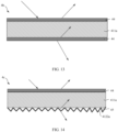
- FIG. 13 is a schematic diagram of a structure of another optical cover plate 4b provided in the related art.
- the optical cover plate 4b includes a substrate 411a and an anti-reflection (anti-reflection, AR) plating layer.
- the AR plating layer 44 is located on two opposite surfaces of the substrate 411a and forms AR plating glass together with the substrate 411a.
- the AR plating glass may alternatively be transmission improving glass or anti-reflection glass. Due to existence of the AR plating layer 44, the AR plating glass has a lower reflection ratio compared with that only the optical cover plate 4a is included, and the reflectances of an inner surface and an outer surface of the optical cover plate 4b may be reduced from 4.2% to 0.5%.
- the reflectances of the inner surface and the outer surface of the optical cover plate 4b are greatly reduced, during photographing by an electronic device 100 bearing the optical cover plate 4b in a general scenario, there is basically no ghosting. However, the inner surface and the outer surface of the optical cover plate 4b still have a reflectance of 0.5%, and there is still obvious ghosting during photographing by the electronic device 100 in a strong contrast environment.
- the inner surface of the optical cover plate 4b has strong hydrophilic performance and oleophilic performance, and it is extremely easy for moisture and small organic molecules to attach to the inner surface, generating the mist-like dirt 43.
- FIG. 14 is still another schematic diagram of a structure of an optical cover plate 4c in the related art.
- the optical cover plate 4c includes a substrate 411a, an AR plating layer 44, and a light trapping layer 45.
- the AR plating layer 44 and the light trapping layer 45 are arranged on two opposite surfaces of the substrate 411a.
- a surface on which the AR plating layer 44 is located forms an outer surface of the optical cover plate 4c, and a surface on which the light trapping layer 45 is located forms an inner surface of the optical cover plate 4c.
- the light trapping layer 45 includes a plurality of protrusions 4122a, a bottom of the protrusion 4122a is connected to the substrate 411a, and a top of the protrusion 4122a is located at an end of the substrate 411a facing away from the AR plating layer 44.
- the plurality of protrusions 4122a are continuously arranged on the substrate 411a to form the light trapping layer 45, so that a surface of the light trapping layer 45 presents a surface morphology in which a plurality of convex points (not marked in the figure) and concave points (not marked in the figure) are alternately and continuously arranged, forming a light trapping effect, to change a reflectance of the surface of the light trapping layer 45 for light.
- the convex point is a vertex of the protrusion 4122, and the concave point is located between adjacent protrusions 4122.
- the air and the material (for example, glass) of the film layer forming the light trapping layer 45 have different refractive indexes, and in the surface morphology in which the plurality of convex points and concave points are alternately and continuously arranged, the proportion of the material of the film layer in the light trapping layer 45 gradually decreases in a direction from the bottom of the protrusion 4122a to the top of the protrusion 4122a, so that the light trapping layer 45 forms a gradient film layer having a gradually changing refractive index.
- the refractive index of the light trapping layer 45 for light gradually changes from a refractive index corresponding to the film layer to a refractive index corresponding to air.
- the reflectance of the inner surface of the optical cover plate 4c can be further reduced from 0.5% to less than 0.03% through arrangement of the light trapping layer 45, and the ghosting intensity during photographing in a strong contrast environment can be reduced by half compared with the AR plating glass.
- the inner surface of the optical cover plate 4c is rougher than an inner surface of the AR plating glass. Because surface energy of the optical cover plate 4c at the convex point is relatively large, when a liquid falls on the inner surface of the optical cover plate 4c, the liquid is easy to aggregate on the convex point to form a liquid drop.
- the surface of the light trapping layer 45 has a hydrophilic property, the liquid drop aggregating on the convex point is pulled off under a syphonage effect, to attach to the convex point and concave point. This easily causes the atoms and molecules of the plating layer and some small molecules of the foam adhesive to attach to and aggregate on the inner surface of the optical cover plate 4c, and forms the mist-like dirt 43 in the light-transmissive area 414.
- FIG. 15 is a schematic diagram of a structure of the optical body layer 41 in FIG. 10 .
- the optical body layer 41 includes a substrate 411 and a first anti-reflection layer 412.
- the substrate 411 may be a glass substrate.
- the glass substrate may be made of original glass, tempered glass, or the like.
- the first anti-reflection layer 412 covers a side of the substrate 411 facing the hydrophobic film layer 42.
- the side of the first anti-reflection layer 412 facing the hydrophobic film layer 42 is a rough surface with a second micro-nano structure 4121.
- a surface of the first anti-reflection layer 412 facing the hydrophobic film layer 42 forms an inner surface of the optical body layer 41.
- the inner surface of the optical body layer 41 is a rough surface with the second micro-nano structure 4121.
- the first micro-nano structure 4211 is adhered to and covers the second micro-nano structure 4121.
- the hydrophobic film layer 42 is located on the rough surface of the first anti-reflection layer 412, to reduce a reflectance of the inner surface of the optical cover plate 4 by using the first anti-reflection layer 412, achieving a light trapping effect for reflection of an inner optical lens of the covered lens 32 and the outer surface of the lens 32, to reduce the ghosting intensity during photographing in a general scenario and in a strong contrast environment, and improve a photographing effect of the camera module 3.
- the hydrophobic rough surface has a rough morphology with a micro-sized and/or nano-sized surface structure, so that the hydrophobic film layer 42 may cover the rough surface of the first anti-reflection layer 412, and the hydrophobic film layer 42 may be combined with the second micro-nano structure 4121, to form the first micro-nano structure 4211 on the surface of the hydrophobic layer 421.
- the liquid drop has an extremely small roll angle on the hydrophobic rough surface, so that the liquid drop aggregating on the first micro-nano structure 4211 can slide out of the light-transmissive area 414 more easily, to reduce the proportion of the mist-like dirt 43 formed in the light-transmissive area 414.
- a shape of the first micro-nano structure 4211 matches a shape of the second micro-nano structure 4121, so that the first micro-nano structure 4211 matching the second micro-nano structure 4121 can be formed on a surface of the hydrophobic layer 421, and the hydrophobic rough surface of the hydrophobic film layer 42 can also have an anti-reflection effect of the first anti-reflection layer 412 without affecting an anti-reflection effect of the first anti-reflection layer 412.
- the hydrophobic rough surface is located in the light-transmissive area 414 of the inner surface of the optical cover plate 4, through matching between the shape of the first micro-nano structure 4211 and the second micro-nano structure 4121, a water drop angle of the inner surface of the optical cover plate 4 in the light-transmissive area 414 is increased, and the inner surface of the optical cover plate 4 further has an anti-reflection effect of the first anti-reflection layer 412 in the light-transmissive area 414.
- a refractive index of the first anti-reflection layer 412 is configured to gradually change from a refractive index corresponding to the first anti-reflection layer to the refractive index corresponding to air in a direction from the substrate 411 to the hydrophobic film layer 42, so that the first anti-reflection layer 412 is a gradient film layer with the refractive index continuously changing in the direction from the substrate 411 to the hydrophobic film layer 42.
- the light trapping effect can further be formed, to absorb the light reflected by the lens 32 to the first anti-reflection layer 412 (which is the light trapping effect) and reduce the ghosting intensity during photographing in a general scenario and in a strong contrast environment.
- the second micro-nano structure 4121 may include a plurality of protrusions 4122.
- a bottom 4123 of the protrusion 4122 is connected to the substrate 411, a top 4124 of the protrusion 4122 is arranged facing the hydrophobic film layer 42, and the protrusion 4122 gradually tapers from the bottom 4123 to the top 4124.
- the protrusion 4122 may be a pyramid, a semi-sphere, or another shape satisfying the foregoing requirement.
- the pyramid may include, but is not limited to, a triangular pyramid, a square pyramid, or a pyramid formed by another number of polygons.
- the triangular pyramid may be regarded as a pyramid shape.
- a shape of protrusion 4122 is not further limited herein.
- the concave point (not marked in the figure) can be formed between two adjacent protrusions 4122, so that a surface morphology of a plurality of convex points (not marked in the figure) and concave points alternately stacked is formed on the inner surface of the optical body layer 41.
- a proportion of a base material of the first anti-reflection layer 412 gradually decreases, and a proportion of air (air at the concave points) in the first anti-reflection layer 412 gradually increases in the direction from the substrate 411 to the hydrophobic film layer 42, so that the refractive index of the first anti-reflection layer 412 for light is gradually changed from the refractive index corresponding to the first anti-reflection layer to the refractive index corresponding to the air in the direction from the substrate 411 to the hydrophobic film layer 42.
- the reflectances of the inner surface of the optical body layer 41 and the inner surface of the optical cover plate 4 for light in the light-transmissive area 414 are reduced, to reduce multi-level reflection of the light in the optical cover plate 4 and the lens 32 and reduce the ghosting intensity during photographing in a strong contrast environment.
- the light trapping effect can be further formed on the surface of the first anti-reflection layer 412 facing the hydrophobic film layer 42, to absorb the light reflected by the lens 32 to the first anti-reflection layer 412, thereby further reducing the ghosting intensity during photographing in a strong contrast environment.
- the second micro-nano structure 4121 can further be formed by using the plurality of protrusions 4122, to increase, by using the second micro-nano structure, the water drop angle of the inner surface of the optical cover plate 4 in the light-transmissive area 414 and reduce the roll angle of the inner surface of the optical cover plate 4 in the light-transmissive area 414.
- Bottoms 4123 of the plurality of protrusions 4122 are connected, so that density of the protrusions 4122 on the surface of the first anti-reflection layer 412 can be increased, and the surface morphology in which a plurality of convex points and concave points are alternately and continuously arranged is formed on the inner surface of the optical body layer 41.
- the foregoing first anti-reflection layer 412 with the continuously changing refractive index is formed, the light trapping effect is enhanced, and the ghosting strength during photographing in a strong contrast environment is further reduced.
- the first anti-reflection layer 412 may be a light trapping layer.
- the protrusion 4122 on the surface of the light trapping layer may be formed by plating a metal film on a to-be-processed plate 4111 and etching after the metal film is contracted.
- the to-be-processed plate 4111 may be understood as a glass plate that is not processed (by etching or corrosion). In this way, while the reflectances of the inner surface of the optical body layer 41 and the inner surface of the optical cover plate 4 for light in the light-transmissive area 414 are reduced, and the ghosting intensity during photographing in a general scenario and in a strong contrast environment is reduced, the structure of the first anti-reflection layer 412 can be more diversified.
- the first anti-reflection layer 412 is the light trapping layer, same as the light trapping layer 45 in the related art, while the reflectance of the inner surface of the optical cover plate 4 can be reduced to less than 0.03% by using the first anti-reflection layer 412, the light trapping effect for reflection of the inner optical lens of the covered lens 32 and the outer surface of the lens 32, so that there is basically no ghosting during photographing in a general scenario, and the ghosting intensity during photographing in a strong contrast environment can be reduced.
- the second micro-nano structure 4121 may further include a plurality of depressions.
- the depressions are micro-sized and/or nano-sized depressions, and the plurality of depressions are uniformly arranged on the optical body layer 41 to form the first anti-reflection layer 412.
- the depression may include, but is not limited to, a hole or a trench on the surface of the first anti-reflection layer 412.
- the first micro-nano structure 4211 is also a hole or a trench matching the shape of the second micro-nano structure 4121.
- a micro morphology of the surface of the first anti-reflection layer 412 can also be changed, and the light trapping layer can be formed.
- the reflectance of the inner surface of the optical cover plate 4 is reduced to less than 0.03%. While the ghosting intensity during photographing in a strong contrast environment is reduced, a relatively protruding convex point may be formed in a connection area between two adjacent depressions, to increase the water drop angle and the oil drop angle of the inner surface of the optical cover plate 4 in the light-transmissive area 414 by using the first micro-nano structure 4211, and reduce the roll angle of the inner surface of the optical cover plate 4 in the light-transmissive area 414.
- the first anti-reflection layer 412 may alternatively be a porous coating layer, so that the structure of the first anti-reflection layer 412 is more diversified.
- the second micro-nano structure 4121 may further include a plurality of micro-sized and/or nano-sized depressions.
- optical cover plate 4 in this application is further described below by using the protrusion 4122 as an example.
- the protrusion 4122 is the micro-sized and/or nano-sized protrusion, facilitating forming the first anti-reflection layer 412 having a micro morphology, to reduce a thickness of the optical cover plate 4.
- a height H of the protrusion 4122 may be greater than or 50 nm and less than or equal to 200 nm, and a size of the bottom 4123 is greater than or 150 nm and less than or equal to 500 nm.
- the height H of the protrusion 4122 may alternatively be greater than or equal to 50 nm and less than or equal to 120 nm, and the size of the bottom 4123 may alternatively be greater than or equal to 170 nm and less than or equal to 500 nm.
- the height H of the protrusion 4122 may be 50 nm, 120 nm, or 200 nm, and the size of the bottom 4123 may be 170 nm, 220 nm, or 500 nm.
- the protrusion can cooperate with the first micro-nano structure 4211 to increase the water drop angle and the oil drop angle of the inner surface of the optical cover plate 4 in the light-transmissive area 414 and reduce the roll angle of the inner surface of the optical cover plate 4 in the light-transmissive area 414.
- the size of the bottom 4123 may be understood as a maximum size or a remote size of the bottom 4123 of the protrusion 4122 along the foregoing X-Y plane. With different shapes of the protrusions 4122, sizes of the corresponding bottoms 4123 are also different. For example, when the protrusion 4122 is a triangular pyramid, the size of the bottom 4123 may be understood as a maximum side length of the bottom 4123 of the triangular pyramid. When the protrusion 4122 is a square pyramid, the size of the bottom 4123 may be understood as a diagonal line of the bottom 4123 of the square pyramid.
- the size of the bottom 4123 may be understood as a diameter of the circle.
- the size of the bottom 4123 may be understood as a diameter of a major axis of the ellipse.
- a thickness D 1 of the hydrophobic layer 421 may be greater than or equal to 5 nm and less than or equal to 30 nm. In some embodiments, the thickness D 1 of the hydrophobic layer 421 may be greater than or equal to 10 nm and less than or equal to 30 nm.
- the plurality of protrusions 4122 are arranged in an array, so that the second micro-nano structure 4121 is formed, and the plurality of protrusions 4122 can be arranged on the inner surface of the optical body layer 41 in a regular manner, facilitating release of stress of the film layer and reducing stress deformation of the optical body layer 41.
- the plurality of protrusions 4122 may be irregularly arranged on the inner surface of the optical body layer 41.
- An arrangement manner of the protrusions 4122 is not further limited in this application.
- FIG. 16 is a schematic exploded view of a part of the optical cover plate 4 according to an embodiment of this application, to facilitate observation of a layered structure in the optical cover plate 4.
- the hydrophobic film layer 42 may further include an underlayer 422.
- the underlayer 422 is attached to the light-transmissive area 414 on a side of the optical body layer 41 facing the optical component (for example, the camera module 3).
- the hydrophobic layer 421 covers the underlayer 422, so that an attachment strength of the hydrophobic layer 421 on the surface of the first anti-reflection layer 412 is increased by using the underlayer 422, thereby enhancing stability of performance of the inner surface of the optical cover plate 4.
- the underlayer 422 is an active underlayer the same as the base material of the first anti-reflection layer 412. Because the active underlayer and the first anti-reflection layer 412 have the same base material, the active underlayer and the first anti-reflection layer 412 have a good bonding strength. In addition, because surface activity of the active underlayer is high, the hydrophobic layer 421 can be adsorbed to the first anti-reflection layer 412, increasing adhesion of the hydrophobic layer 421 to the first anti-reflection layer 412, so that the hydrophobic layer 421 is stably adsorbed to the first anti-reflection layer 412, and is not easy to fall off.
- the base material of the first anti-reflection layer 412 may be silicon dioxide or another light-transmissive optical base material.
- the underlayer 422 may be a silicon dioxide layer. Because the silicon dioxide layer and the base material of the first anti-reflection layer 412 are the same, and are both silicon dioxide, the base materials of the underlayer 422 and the first anti-reflection layer 412 are matched.
- the underlayer 422 can achieve a relatively high surface activity, to adsorb the hydrophobic layer 421 to the first anti-reflection layer 412 and increase the adhesion of the hydrophobic layer 421 on the first anti-reflection layer 412.
- a surface of the underlayer 422 facing the hydrophobic layer 421 has a third micro-nano structure 4221.
- the third micro-nano structure 4221 covers the second micro-nano structure 4121 and is attached between the second micro-nano structure 4121 and the first micro-nano structure 4211.
- a shape of the third micro-nano structure 4221 matches the shape of the second micro-nano structure 4121.
- the adhesion of the hydrophobic layer 421 on the first anti-reflection layer 412 is enhanced by using the underlayer 422
- consistency of the first micro-nano structure 4211 and the second micro-nano structure 4121 can be ensured due to arrangement of the third micro-nano structure 4221, so that while the water drop angle and the oil drop angle of the inner surface of the optical cover plate 4 in the light-transmissive area 414 are increased, the arrangement of the first micro-nano structure 4211 can be prevented from affecting transmission of light in the optical cover plate 4, thereby ensuring a photographing effect of the camera module 3.
- a thickness D 2 of the underlayer 422 may be less than the thickness D 1 of the hydrophobic layer 421.
- the thickness D 2 of the underlayer 422 may be greater than or equal to 8 nm and less than or equal to 13 nm.
- the thickness D 2 of the underlayer 422 may be greater than or equal to 3 nm and less than or equal to 13 nm.
- the optical body layer 41 further includes a second anti-reflection layer 413.
- the second anti-reflection layer 413 is light-transmissive and is located on a surface of the substrate 411 facing away from the hydrophobic film layer 42.
- a surface of the second anti-reflection layer 413 facing away from the substrate 411 forms the optical body layer 41 and an outer surface of the optical cover plate 4.
- the outer surface of the optical cover plate 4 may be used as a light-incident surface. In this way, through arrangement of the second anti-reflection layer 413, reflection of light by the outer surface of the optical cover plate 4 can be reduced, protecting the outer surface of the optical cover plate 4 from being scratched.
- the second anti-reflection layer 413 may be an optical anti-reflection film system.
- the optical anti-reflection film system may include, but is not limited to, an ordinary optical AR film system, a hard AR film system, and an anti-scratch AR film system.
- the ordinary optical AR film system may be understood as an AR film system having only optical performance such as anti-reflection. Because the ordinary optical AR film system, the hard AR film system, and the anti-scratch AR film system may be considered as AR plating layers 44, the reflectance of the outer surface of the optical cover plate 4 can be reduced from 0.5% to less than 0.3% through the arrangement of the second anti-reflection layer 413.
- the reflectance of the inner surface of the optical cover plate 4 in this application may be reduced to less than 0.03%, and the reflectance of the outer surface may be reduced to less than 0.3%. This can effectively prevent ghosting from being generated during photographing by the electronic device 100 in a general scenario and in a strong contrast scenario.
- FIG. 17 is a schematic diagram of layers of the second anti-reflection layer 413, and does not constitute a limitation on a quantity of layers of the second anti-reflection layer 413.
- the second anti-reflection layer 413 includes a first film layer 4131 and a second film layer 4132 with a refractive index greater than a refractive index of the first film layer 4131.
- the first film layer 4131 and the second film layer 4132 are alternately stacked on the substrate 411 of the optical body layer 41, to form the second anti-reflection layer 413.
- the first film layer 4131 is located on a surface layer of the second anti-reflection layer 413. In this way, while the reflectance of the outer surface of the optical cover plate 4 is low, ghosting is effectively prevented from being generated during photographing by the electronic device 100 in a general scenario and a strong contrast scenario
- the second anti-reflection layer 413 adopts a film stack 2H (two film materials).
- the first film layer 4131 may be made of a film material with high hardness and a relatively low refractive index, such as silicon dioxide
- the second film layer 4132 may be made of a film material with a refractive index greater than a refractive index of the first film layer 4131, such as silicon nitride.
- the outer surface of the optical cover plate 4 can have some hardness, to protect the outer surface of the optical cover plate 4 from being scratched.
- the optical performance (such as a reflectance and transmittance) of the optical cover plate 4 is separately tested by using a spectrophotometer.
- a light wave with a wavelength ranging from 380 nm to 780 nm as an example, the reflectance of the optical cover plate 4 is less than 0.3%, and the transmittance of the optical cover plate 4 is greater than 98%.
- a chrominance meter is used to test chrominance of reflected light and transmitted light of the optical cover plate 4.
- L* represents luminance
- a* represents red and green
- b* represents yellow and blue.
- a test result shows that in a color value of the reflected light, a deviation of a value a is within ⁇ 2, and a deviation of a value b is within ⁇ 2; in a color value of the transmitted light, a deviation of a value a is within ⁇ 2, and a deviation of a value b is within ⁇ 2. It can be seen from this that the color of visible light after the visible light is transmitted through the optical cover plate 4 and is reflected by the optical cover plate 4 is not affected, and the original color remains, to ensure accuracy of photographing an object by the covered camera module 3.
- an embodiment of this application further provides a preparation method for an optical assembly.
- the preparation method is applied to the foregoing optical assembly.
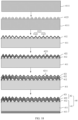
- FIG. 18 is a schematic diagram of changing of a structure of the optical cover plate 4 in an optical assembly during preparation
- FIG. 19 is a flowchart of a preparation method of the optical cover plate 4.
- the preparation method for an optical assembly includes:
- the surface of the optical stack on which the hydrophobic rough surface is arranged has a hydrophobic property in the light-transmissive area 414 of the optical body layer 41. Because the hydrophobic rough surface is arranged facing the optical component, the surface of the optical stack on which the hydrophobic rough surface is arranged may be used as an inner surface of the optical cover plate 4, and the light-transmissive area 414 of the optical body layer 41 may be used as a light-transmissive area 414 of the optical cover plate 4.
- the light-transmissive area of the optical stack is located at a position opposite to the optical component (for example, the camera module 3) that is blocked by the light-transmissive area, so that ambient light is transmitted through the light-transmissive area of the optical stack and enters the optical component.
- the optical component for example, the camera module 3
- the preparing the optical stack in step S100 may specifically include: processing a surface of a to-be-processed plate 4111 to form the optical stack, where the to-be-processed plate is an unprocessed glass plate.
- the optical stack may include a substrate 411 and a first anti-reflection layer 412, the first anti-reflection layer 412 covers a side of the substrate 411 facing the hydrophobic film layer 42, a side of the first anti-reflection layer 412 facing the hydrophobic film layer 42 is a rough surface with a second micro-nano structure 4121, and the hydrophobic film layer 42 is located on the first anti-reflection layer 412 and covers light-transmissive area 414 on the first anti-reflection layer 412 corresponding to the optical body layer 41.
- the processing on the to-be-processed plate 4111 may include, but is not limited to, etching or corrosion.
- the first anti-reflection layer 412 due to existence of the second micro-nano structure 4121, it is facilitate to formation of the first micro-nano structure 4211 on the hydrophobic film layer 42, to increase a water drop angle and an oil drop angle of the optical cover plate 4 on the surface of the hydrophobic film layer 42, reduce a roll angle, and reduce a proportion of mist-like dirt occurring on the optical cover plate 4 in the light-transmissive area 414, and the reflectance of the surface of the hydrophobic film layer 42 can be reduced, to reduce ghosting intensity during photographing in a general scenario and in a strong contrast environment.
- a corresponding processing method may be adopted for processing the surface of the to-be-processed plate 4111 based on a difference of a structure of the second micro-nano structure 4121.
- the method for processing the surface of the to-be-processed plate 4111 is further described below with reference to the second micro-nano structures 4121 of different structures.
- the second micro-nano structure 4121 includes a plurality of protrusions 4122.
- the protrusion 4122 is a micro-sized and/or nano-sized protrusion, or the second micro-nano structure 4121 includes a plurality of depressions, where the depressions are micro-sized and/or nano-sized depressions.
- the plurality of protrusions 4122 may be obtained by using a surface processing method well-known by a person skilled in the art by using processing methods such as metal masking, diamond flycutting, and chemical corrosion. This is not specially limited in this application.
- the processing the surface of the to-be-processed plate 4111 to form the optical stack may specifically include:
- a part not covered by the particles 4125 on the to-be-processed plate 4111 can be etched through metal masking, to form the optical stack including the substrate and the plurality of second micro-nano structures 4121.
- a layered structure in which the plurality of second micro-nano structures 4121 are located forms the first anti-reflection layer 412, points at which the plurality of second micro-nano structures 4121 are located form convex points on the surface of the first anti-reflection layer 412, and points between the second micro-nano structures 4121 form convex points on the surface of the first anti-reflection layer 412, so that the first anti-reflection layer 412 forms a gradient film layer.
- the first anti-reflection layer 412 may be a light trapping layer, to reduce a reflectance of the inner surface of the optical cover plate 4 and reduce ghosting during photographing by the electronic device 100, and can cooperate with the hydrophobic film layer 42 to increase the water drop angle and the oil drop angle of the inner surface of the optical cover plate 4 in the light-transmissive area 414, reduce the roll angle of the inner surface of the optical cover plate 4 in the light-transmissive area 414, and reduce the proportion of mist-like dirt 43 in the light-transmissive area 414.
- a metal film may be formed on the to-be-processed plate 4111 through vacuum deposition or liquid coating.
- the vacuum deposition may include, but is not limited to, chemical gas phase deposition, physical gas phase deposition, thermal deposition, electron beam vaporization deposition, atomic layer deposition, or the like.
- the chemical gas phase deposition may include, but is not limited to, vacuum evaporation, and the physical gas phase deposition may include, but is not limited to, sputter deposition.
- the liquid coating may include, but is not limited to, manners such as spraying, dip coating, and spin coating.
- the metal film may include, but is not limited to, a molybdenum film, an indium film, or the like.
- process parameters required for forming the molybdenum film can be first set in a plating machine.
- the process parameters include, but are not limited to, a film thickness, a vacuum degree, temperature, sputter power, gas flow rate, time, and the like.
- the to-be-processed plate 4111 to be coated is then loaded onto a substrate rack and placed in the plating machine. After vacuuming and inputting a corresponding degree, the plating is completed.
- a molybdenum target and gas are turned off, and when the vacuum degree reaches a preset parameter, the molybdenum film is heat treated (such as heated).
- Parameters during heat treatment such as a temperature rising speed, a maintained temperature after the heating, and a temperature-maintaining time, may be set, to obtain a particle template of particles with a preset diameter.
- a part on which the particle 4125 is not arranged on the particle template may be etched by using a method such as plasma etching, to form a plurality of nano-sized protrusions 4122 (nano protrusions) with a specific height and a specific bottom size, at a position at which the surface of the particle template is covered by the particle 4125.
- the plurality of protrusions 4122 are connected to form the second micro-nano structure 4121.
- the performing cleaning processing on the particle template may specifically include: at room temperature, the cleaning processing is performed on the molybdenum film on the surface of the protrusion 4122 by using a deplating solution, to obtain the optical stack having the first anti-reflection layer 412.
- a parameter of forming the molybdenum film through the vacuum sputter, a parameter of the heat treatment, and a parameter of the plasma etching are not specifically limited, and a person skilled in the art may select the parameter based on a requirement.
- a film thickness of the molybdenum film may range from 3 nm to 8 nm.
- a heating rate of the heat treatment ranges from 15°C/min to 25°C/min, heating is performed to 100°C to 200°C, and temperature is maintained for 6 min to 10 min.
- the height of the protrusion 4122 formed through etching may range from 50 nm to 200 nm, and the size of the bottom 4123 may range from 150 nm to 450 nm.
- the performing processing on the surface of the to-be-processed plate 4111 to form the optical stack may specifically further include: performing chemical corrosion on the to-be-processed plate 4111, and forming the second micro-nano structure 4121 on a surface of the to-be-processed plate 4111.
- a part of the second micro-nano structure 4121 is the first anti-reflection layer 412, and a part other than the first anti-reflection layer 412 in the optical stack is the substrate 411.
- the second micro-nano structure 4121 can be formed on the surface of the to-be-processed plate 4111 through chemical corrosion, to increase the water drop angle and the oil drop angle of the inner surface of the optical cover plate 4 in the light-transmissive area 414 while reducing the reflectance of the inner surface of the optical cover plate 4 in the light-transmissive area 414.
- the first anti-reflection layer 412 formed through the chemical etching may alternatively be the light trapping layer.
- the performing chemical corrosion on the to-be-processed plate 4111 may specifically include: after cleaning the surface of the to-be-processed plate 4111, the to-be-processed plate 4111 is first placed in a corrosion tank containing a first corrosion liquid for first preset time and taken out to be cleaned, the to-be-processed plate 4111 is then placed in a corrosion tank containing a second corrosion liquid for second preset time and taken out to be cleaned, and finally, the to-be-processed plate 4111 is dried. After the to-be-processed plate is cooled, an optical stack with a single-side reflectance less than 0.03% is obtained. The optical stack may also be referred to as anti-reflection glass.
- the first corrosion liquid may include a mixed solution including HF at a concentration of 0.001% and HCl at a concentration of 1%
- the second corrosion liquid may include a mixed solution including HF at a concentration of 0.001% and Na 2 SiO 3 at a concentration of 0.0001%.
- a porous coating layer may be further coated on the to-be-processed plate 4111, to form the optical stack.
- the porous coating layer may be understood as the first anti-reflection layer 412 in the optical stack
- the to-be-processed plate 4111 may be understood as the substrate 411 in the optical stack.
- FIG. 20 is a flowchart of a preparation method for the hydrophobic film layer 42 in the optical cover plate 4.
- the forming the hydrophobic film layer 42 on the surface of the optical stack specifically includes: Step S210: Form the hydrophobic layer with the first micro-nano structure on the surface of the substrate with the second micro-nano structure, where the first micro-nano structure is located on the second micro-nano structure and covers the light-transmissive area on the first anti-reflection layer corresponding to the optical body layer, a surface of the hydrophobic layer facing the optical component is the hydrophobic rough surface, and the hydrophobic film layer includes the hydrophobic layer.
- the hydrophobic rough surface can be formed on the surface of the hydrophobic layer 421 facing the optical component, so that while the reflectance of the substrate 411 on the surface of the first anti-reflection layer 412 is not affected, the optical stack has hydrophobic and oleophobic functions on the hydrophobic rough surface, to be bonded with the first micro-nano structure 4211. Therefore, the water drop angle and the oil drop angle of the inner surface of the optical cover plate 4 in the light-transmissive area 414 are increased, and the roll angle of the inner surface of the optical cover plate 4 in the light-transmissive area 414 is reduced, thereby reducing the proportion of the mist-like dirt 43 formed on the inner surface of the optical cover plate 4.
- the hydrophobic layer 421 may be formed on the second micro-nano structure 4121 of the substrate 411 through vacuum deposition or liquid coating.
- the hydrophobic layer 421 may include, but is not limited to, a perfluoropolyethers layer.
- vacuum evaporation may be used in this application, and a parameter in a vacuum evaporation process is set based on a desired thickness of the perfluoropolyethers layer, so that perfluoropolyethers is heated and vaporized, thereby condensing on the second micro-nano structure 4121 of the substrate 411 to form an anti-pollution hydrophobic layer 421.
- the thickness of the perfluoropolyethers layer and the parameter for forming the perfluoropolyethers layer through the vacuum evaporation are not specially limited in embodiments of this application, and may be selected by a person skilled in the art based on a requirement.
- the thickness of the perfluoropolyethers layer may range from 10 nm to 30 nm.
- the preparation method may further include: Step S201: Form an underlayer with a third micro-nano structure on the surface of the substrate with the second micro-nano structure, where the third micro-nano structure covers the second micro-nano structure and is adhered between the second micro-nano structure and the first micro-nano structure, and the hydrophobic film layer further includes the underlayer.
- the underlayer 422 has good bonding strength on the first anti-reflection layer 412, and because the underlayer 422 has high surface activity, the underlayer 422 can adsorb the hydrophobic layer 421 to the first anti-reflection layer 412, increasing adhesion of the hydrophobic layer 421 on the first anti-reflection layer 412, so that the hydrophobic layer 421 is stably adsorbed to the first anti-reflection layer 412, and is not easy to fall off.
- a material, a thickness, and the like of the underlayer 422 refer to related descriptions above, and details are not described herein again.
- the underlayer 422 may be formed on the first anti-reflection layer 412 through vacuum deposition or liquid coating.
- the underlayer 422 may be formed through sputter plating.
- a parameter of the sputter plating for forming the underlayer 422 is not specially limited in embodiments of this application, and may be selected by a person skilled in the art based on a requirement.
- the thickness of the underlayer 422 may range from 8 nm to 13 nm.
- the preparation method further includes: forming a second anti-reflection layer 413 on a surface of the optical stack facing away from the hydrophobic film layer 42, where the optical body layer 41 further includes the second anti-reflection layer 413.
- the optical cover plate 4 includes the optical body layer 41 and the hydrophobic film layer 42, through arrangement of the second anti-reflection layer 413, a reflectance of the surface (namely, an outer surface of the optical cover plate 4) of the optical body layer 41 facing away from the hydrophobic film layer 42 can be reduced to less than 0.3%, thereby effectively preventing ghosting from being generated during photographing of the electronic device 100 in a general scenario and a strong contrast scenario, and further protecting the outer surface of the optical cover plate 4 from being scratched.
- the second anti-reflection layer 413 reference may be made to the foregoing related descriptions, and details are not further described herein.
- film design software such as TFCALC and Macleod may be used to design the film based on optical requirements, and deposition is then performed based on a designed film structure, so that the second anti-reflection layer 413 formed through deposition can satisfy a requirement in which an average single-sided reflectance of visible light in a band ranging from 380 nm to 780 nm is less than 0.3%, ensuring that the visible light in this band has high transmittance.
- a film stack 2H may be used, and a second film layer 4132 is made of a film material with high hardness and a relatively low refractive index.
- the film material of the second film layer 4132 may be SiO 2 .
- a first film layer 4131 is made of a film material with a refractive index less than a refractive index of the second film layer 4132.
- the film material of the first film layer 4131 may be Si 3 N 4 .
- An initial film system is formed in optical thin film software, so that a film system in which the first film layer 4131 and the second film layer 4132 are alternately stacked is formed.
- a band optimization condition is input to continuous targets, to ensure that the transmittance and the reflectance satisfy requirements.
- a Lab value requirement is input to a color target, to ensure that a color of transmitted light is colorless, and the second anti-reflection layer 413 satisfying the foregoing requirement is obtained after a series of optimization designs.
- a vacuum sputter plating machine may be used to plate the optical stack on which the hydrophobic film layer 42 is formed, to form the optical cover plate 4 having the second anti-reflection layer 413.
- Plating parameters may be selected based on a material of each layer of the film system structure. This is not specially limited in this application.
- plating parameters of the first film layer 4131 may be: sputter power of a silicon target: 7000 W to 8000 W, a flow rate of Ar: 100 sccm to 150 sccm, a flow rate of N 2 : 50 sccm to 100 sccm, and power of a Radical Source (radical ion source): 4000 W to 5000 W.
- Plating parameters of the second film layer 4132 may be: sputter power of a silicon target: 7500 W to 8500 W, a flow rate of Ar: 200 sccm to 300 sccm, a flow rate of O 2 : 100 sccm to 150 sccm; and power of a Radical Source: 4000 W to 5000 W.
- the second anti-reflection layer 413 may be first formed on the surface of the optical stack facing away from the first anti-reflection layer 412, and the hydrophobic film layer 42 is finally formed on the first anti-reflection layer 412 of the optical stack.
- the second anti-reflection layer 413 may be first formed on a surface of a to-be-processed plate 4111, and the first anti-reflection layer 412 and the hydrophobic film layer 42 are sequentially formed on the other surface of the to-be-processed plate 4111.
- a preparing sequence of the second anti-reflection layer 413 is not further limited.
- Step 1 Vacuum sputter of a molybdenum film on the to-be-processed plate
- a film thickness of the molybdenum film was set to 5 nm, and was input to a plating machine. Then, process parameters were set as follows: background vacancy was 5.0 ⁇ 10 -4 Pa, and temperature was set to 80°C; and to strengthen adhesion between the film layer and the to-be-processed plate 4111, pre-processing was performed by using radio frequency (RF) magnetron sputter before plating, and specific parameters were as follows: power of a Radical Source was 4500 W, a flow rate of Ar was 0 sccm, a flow rate of O 2 was 120 sccm, a flow rate of N 2 was 0 sccm, and time was 240s.
- RF radio frequency
- plating parameters were set as follows: molybdenum target sputter power was 3000 W, and the flow rate of Ar was 120 sccm.
- the to-be-processed plate 4111 to be plated was loaded onto a substrate rack, and was placed in the foregoing plating machine; a door was closed to evacuate, a plating program was input, and film formation (plating metal molybdenum) was started by clicking, to complete plating.
- Step 2 Performing heat treatment on the molybdenum film
- Step 3 Plasma etching
- Step 4 Cleaning and removing a residual molybdenum film
- Cleaning processing was performed on the residual molybdenum film layer by using a deplating solution at a room temperature, and then the surface of the to-be-processed plate 4111 was cleaned by using pure water, to obtain an optical stack with a low single-side reflectance and a high transmittance.
- the transmittance of visible light on the formed optical stack is 90%, and the reflectance of the surface of the optical stack with the second micro-nano structure 4121 decreases to less than 0.03%.
- Step 1 Plasma surface treatment
- Step 2 Plating the underlayer
- the underlayer 422 Using a silicon dioxide layer as an example, to obtain the underlayer 422, background vacuum was 5.0 ⁇ 10 -3 Pa, and parameters of magnetron sputter plating were set as follows: sputter power of a silicon target was 8 kW, the flow rate of Ar was 250 sccm, the flow rate of Ar was 250 sccm, the flow rate of O 2 was 120 sccm, and plating time was 2 min. According to the foregoing plating process of vacuum sputter of the molybdenum film on the to-be-processed plate 4111, the underlayer 422 with a thickness ranging from 8 nm to 13 nm was obtained.
- Step 3 Plating the hydrophobic layer
- perfluoropolyethers layer As an example, to obtain the anti-pollution hydrophobic layer 421, parameters of the vacuum evaporation were set as follows: a plating current was 260 A, the flow rate of Ar was 220 sccm, the flow rate of O 2 was 220 sccm, and the plating time was 3 min.
- a plating current was 260 A
- the flow rate of Ar was 220 sccm
- the flow rate of O 2 was 220 sccm
- the plating time was 3 min.
- Step 1 Designing a film system structure
- Film system design of the second anti-reflection layer 413 is based on TFCALC.
- An average single-side reflectance of 380 nm to 780 nm is required to be less than 0.3%. Due to a high transmittance requirement for the visible light band, the film stack 2H is used in the film system.
- the film material of the first film layer 4131 (L) is made of SiO 2 with high hardness and a relatively low refractive index
- the film material of the second film layer 4132 (H) is made of Si 3 N 4 .
- An initial film system LH is formed in the optical thin film software. In this way, a film system in which the first film layer 4131 and the second film layer 4132 are alternately stacked is formed.
- Table 1 shows a film system structure of an optical cover plate including a second anti-reflection layer of a first film system Structure Stack Material 550 nm refractive index Physical thickness (nm) Outer surface Environment Air 1.0003 / Second anti-reflection layer SiO 2 1.4541 97.35 Si 3 N 4 1.9562 144.56 SiO 2 1.4541 199.72 Si 3 N 4 1.9562 33.4 SiO 2 1.4541 17.75 Si 3 N 4 1.9562 2158.76 SiO 2 1.4541 13.36 Si 3 N 4 1.9562 42.44 SiO 2 1.4541 39.71 Si 3 N 4 1.9562 16.57 SiO 2 1.4541 30 Base material Glass 1.5163 / First anti-reflection layer Glass Continuously changing refractive index 100 nm Inner surface Hydrophobic layer Perfluoropolyethers 1.3 10 nm
- Step 2 A second anti-reflection layer 413 was formed on the substrate 411, a film thickness of each layer in the second anti-reflection layer 413 designed in Table 1 was input to the plating machine, and process parameters were set as follows: background vacancy was 5.0 ⁇ 10 -4 , and temperature was set to 80 centigrade.
- pre-processing was performed by using RF before the plating, and specific parameters were as follows: the power of the Radical Source was 4500 W, the flow rate of Ar was 0 sccm, the flow rate of O 2 was 120 sccm, the flow rate of N 2 was 0 sccm, and time was 240s.
- the parameters of plating were set as follows: sputter power of a silicon target was 8000 W, the flow rate of Ar was 250 sccm, the power of the Radical Source was 4500 W, the flow rate of Ar was 250 sccm, and the flow rate of O 2 was 120 sccm.
- a high-performance optical cover plate 4 with transmittance of 98.45%, a reflectance of an outer surface less than 0.3%, a water drop angle in the light-transmissive area of the inner surface greater than 150°, a reflectance of the inner surface less than 0.03%, Vickers hardness of the outer surface of 1580 HV, hardness of 1300 gram-force, and Mohs hardness of 7 was obtained.
- Step 1 Vacuum sputter of a molybdenum film on the to-be-processed plate
- a film thickness of the molybdenum film was set to 5 nm, and was input to a plating machine. Then, process parameters were set as follows: background vacancy was 5.0 ⁇ 10 -4 Pa, and temperature was set to 80°C. to strengthen adhesion between the film layer and the to-be-processed plate 4111, pre-processing was performed by using radio frequency (RF) magnetron sputter before plating, and specific parameters were as follows: power of a Radical Source was 4500 W, a flow rate of Ar was 0 sccm, a flow rate of O 2 was 120 sccm, a flow rate of N 2 was 0 sccm, and time was 240s.
- RF radio frequency
- the plating parameters were set as follows: sputter power of a molybdenum target was 3000 W, and a flow rate of Ar was 120 sccm.
- the to-be-processed plate 4111 to be plated was loaded onto a substrate rack, and was placed in the foregoing plating machine; a door was closed to evacuate, a plating program was input, and film formation (plating metal molybdenum) was started by clicking, to complete plating.
- Step 2 Performing heat treatment on the molybdenum film
- Step 3 Plasma etching
- Step 4 Cleaning and removing a residual molybdenum film
- Cleaning processing was performed on the residual molybdenum film layer by using a deplating solution at a room temperature, and then the surface of the to-be-processed plate 4111 was cleaned by using pure water, to obtain an optical stack with a low single-side reflectance and a high transmittance.
- the transmittance of visible light on the formed optical stack is 98.45%, and the reflectance of the surface of the optical stack with the second micro-nano structure 4121 decreases to less than 0.03%.
- Step 1 Plasma surface treatment
- Step 2 Plating the underlayer
- the underlayer 422 Using a silicon dioxide layer as an example, to obtain the underlayer 422, background vacuum was 5.0 ⁇ 10 -3 Pa, and parameters of magnetron sputter plating were set as follows: sputter power of a silicon target was 8 kW, the flow rate of Ar was 250 sccm, the flow rate of Ar was 250 sccm, the flow rate of O 2 was 120 sccm, and plating time was 2 min. According to the foregoing plating process of vacuum sputter of the molybdenum film on the to-be-processed plate 4111, the underlayer 422 with a thickness ranging from 3 nm to 13 nm was obtained.
- Step 3 Plating the hydrophobic layer
- perfluoropolyethers layer As an example, to obtain the anti-pollution hydrophobic layer 421, parameters of the vacuum evaporation were set as follows: a plating current was 260 A, the flow rate of Ar was 220 sccm, the flow rate of O 2 was 220 sccm, and the plating time was 3 min.
- a plating current was 260 A
- the flow rate of Ar was 220 sccm
- the flow rate of O 2 was 220 sccm
- the plating time was 3 min.
- Step 1 Designing a film system structure
- Film system design of the second anti-reflection layer 413 is based on TFCALC.
- An average single-side reflectance of 380 nm to 780 nm is required to be less than 0.3%. Due to a high transmittance requirement for the visible light band, the film stack 2H is used in the film system.
- the film material of the first film layer 4131 (L) is made of SiO 2 with high hardness and a relatively low refractive index
- the film material of the second film layer 4132 (H) is made of Si 3 N 4 .
- An initial film system LH is formed in the optical thin film software. In this way, a film system in which the first film layer 4131 and the second film layer 4132 are alternately stacked is formed.
- Table 2 shows a film system structure of an optical cover plate including a second anti-reflection layer of a second film system Structure Stack Material 550 nm refractive index Physical thickness (nm) Outer surface Environment Air 1.0003 / Second anti-reflection layer SiO 2 1.4541 84.88 Si 3 N 4 1.9562 136.14 SiO 2 1.4541 31.86 Si 3 N 4 1.9562 15.66 SiO 2 1.4541 10 Base material Glass 1.5163 / First anti-reflection layer Glass Continuously changing refractive index 100 nm Inner surface Hydrophobic layer Perfluoropolyethers 1.3 10 nm
- Step 2 A second anti-reflection layer 413 was formed on the substrate 411, a film thickness of each layer in the second anti-reflection layer 413 designed in Table 2 was input to the plating machine, and process parameters were set as follows: background vacancy was 5.0 ⁇ 10 -4 , and temperature was set to 80 centigrade.
- pre-processing was performed by using RF before the plating, and specific parameters were as follows: the power of the Radical Source was 4500 W, the flow rate of Ar was 0 sccm, the flow rate of O 2 was 120 sccm, the flow rate of N 2 was 0 sccm, and time was 240s.
- the parameters of plating were set as follows: sputter power of an Aluminum target was 7500 W, the flow rate of Ar was 120 sccm, and the flow rate of N 2 was 80 sccm, and the power of the Radical Source was 4500 W.
- the parameters of plating were set as follows: sputter power of a silicon target was 8000 W, the flow rate of Ar was 250 sccm, the power of the Radical Source was 4500 W, the flow rate of Ar was 250 sccm, and the flow rate of O 2 was 120 sccm.
- an optical cover plate 4 with transmittance 98.45%, a reflectance of an outer surface less than 0.3%, a water drop angle in the transmitting area of the inner surface greater than 150°, and a reflectance of the inner surface less than 0.03% was obtained.
- the surface of the to-be-processed plate 4111 was cleaned by using a cleaning agent, and then cleaned by using deionized water.
- the to-be-processed plate 4111 after being cleaned was placed in a corrosion tank containing a first corrosion liquid for 3 h, and was taken out to be cleaned by using the deionized water, for example, the first corrosion liquid was a mixed solution including HF at a concentration of 0.001% and HCl at a concentration of 1%.
- the to-be-processed plate 4111 after being cleaned again was placed in a corrosion tank containing a second corrosion liquid for 20 h, and was taken out to be cleaned by using the deionized water, for example, the second corrosion liquid was a mixed solution including HF at a concentration of 0.001% and Na 2 SiO 3 at a concentration of 0.0001%.
- the to-be-processed plate 4111 after being cleaned again was placed in a drying oven at 300°C, and was dried for 60 min, a heat switch of the oven was turned off. When the temperature is reduced to 50°C, the to-be-processed plate 4111 was taken out of the oven, to obtain an optical stack with a single-side reflectance less than 0.03%.
- the optical stack was single-side anti reflection glass.
- a surface of the prepared optical stack had a plurality of depressions.
- the depressions were micro-sized and/or nano-sized depressions, and the plurality of depressions formed the second micro-nano structure 4121.
- a layer on which the second micro-nano structure 4121 was located was the first anti-reflection layer 412.
- Step 1 Plasma surface treatment
- Step 2 Plating the underlayer
- the underlayer 422 Using a silicon dioxide layer as an example, to obtain the underlayer 422, background vacuum was 5.0 ⁇ 10 -3 Pa, and parameters of magnetron sputter plating were set as follows: sputter power of a silicon target was 8 kW, the flow rate of Ar was 250 sccm, the flow rate of Ar was 250 sccm, the flow rate of O 2 was 120 sccm, and plating time was 2 min. According to the foregoing plating process of vacuum sputter of the molybdenum film on the to-be-processed plate 4111, the underlayer 422 with a thickness ranging from 8 nm to 13 nm was obtained.
- Step 3 Plating the hydrophobic layer
- perfluoropolyethers layer As an example, to obtain the anti-pollution hydrophobic layer 421, parameters of the vacuum evaporation were set as follows: a plating current was 260 A, the flow rate of Ar was 220 sccm, the flow rate of O 2 was 220 sccm, and the plating time was 3 min.
- a plating current was 260 A
- the flow rate of Ar was 220 sccm
- the flow rate of O 2 was 220 sccm
- the plating time was 3 min.
- Step 1 Designing a film system structure
- Table 3 shows a film system structure of an optical cover plate including a second anti-reflection layer of a third film system Structure Stack Material 550 nm refractive index Physical thickness (nm) Outer surface Environment Air 1.0003 / Second anti-reflection layer SiO 2 1.4541 84.88 Si 3 N 4 1.9562 136.14 SiO 2 1.4541 31.86 Si 3 N 4 1.9562 15.66 SiO 2 1.4541 10 Base material Glass 1.5163 / First anti-reflection layer Glass Continuously changing refractive index 100 nm Inner surface Anti-fouling layer Perfluoropolyethers 1.3 10 nm
- Step 2 A second anti-reflection layer 413 was formed on the substrate 411, a film thickness of each layer in the second anti-reflection layer 413 designed in Table 3 is input to the plating machine, and process parameters were set as follows: background vacancy was 5.0 ⁇ 10 -4 , and temperature was set to 80 centigrade.
- pre-processing was performed by using RF before the plating, and specific parameters were as follows: the power of the Radical Source was 4500 W, the flow rate of Ar was 0 sccm, the flow rate of O 2 was 120 sccm, the flow rate of N 2 was 0 sccm, and time was 240s.
- the parameters of plating were set as follows: sputter power of an Aluminum target was 7500 W, the flow rate of Ar was 120 sccm, and the flow rate of N 2 was 80 sccm, and the power of the Radical Source was 4500 W.
- the parameters of plating were set as follows: sputter power of a silicon target was 8000 W, the flow rate of Ar was 250 sccm, the power of the Radical Source was 4500 W, the flow rate of Ar was 250 sccm, and the flow rate of O 2 was 120 sccm.
- a high-performance optical cover plate 4 with transmittance of 98.45%, a reflectance of an outer surface less than 0.3%, a water drop angle in the transmitting area of the inner surface greater than 150°, a reflectance of the inner surface less than 0.03%, Vickers hardness of the outer surface of 1580 HV, hardness of 1300 gram-force, and Mohs hardness of 7 was obtained.
- a housing and the optical assembly according to any one of the foregoing aspects can be used.
- An optical component in the optical assembly is located in an accommodating space of the housing 2.
- An optical cover plate 4 is located on the housing 2 to replace an original optical cover plate 4a, and covers a light-incident surface 321 of the optical component.
- the optical component for example, the camera module 3
- the optical component for example, the camera module 3
- a water drop angle of an inner surface of the optical cover plate 4 in a light-transmissive area 414 is greater than 150°, effectively reducing a proportion of mist-like dirt 43 formed on the inner surface of the optical cover plate 4.
- the terms “mounting”, “connected”, and “connecting” should be understood broadly, for example, which may be a fixed connection, an indirect connection through an intermediary, or internal communication inside two components or an interaction relationship between two components.
- mounting should be understood broadly, for example, which may be a fixed connection, an indirect connection through an intermediary, or internal communication inside two components or an interaction relationship between two components.
- connecting should be understood broadly, for example, which may be a fixed connection, an indirect connection through an intermediary, or internal communication inside two components or an interaction relationship between two components.
Landscapes
- Physics & Mathematics (AREA)
- General Physics & Mathematics (AREA)
- Optics & Photonics (AREA)
- Chemical & Material Sciences (AREA)
- Chemical Kinetics & Catalysis (AREA)
- Engineering & Computer Science (AREA)
- Multimedia (AREA)
- Signal Processing (AREA)
- Electromagnetism (AREA)
- Inorganic Chemistry (AREA)
- Surface Treatment Of Optical Elements (AREA)
- Optical Elements Other Than Lenses (AREA)
Abstract
Description
- This application claims priority to
Chinese Patent Application No. 202211202910.9, filed with the China National Intellectual Property Administration on September 29, 2022 - This application relates to the field of electronic device technologies, and in particular, to an optical assembly, an optical assembly preparation method, and an electronic device.
- A camera module has become a necessary functional module in an electronic device such as a mobile phone, a tablet computer, a notebook computer, or a wearable device. With continuous development of electronic devices, people's requirements on the photographing effect of the camera module gradually increase.
- The camera module usually includes a module body and an optical cover plate. The module body is arranged inside a housing of the electronic device. The optical cover plate may be arranged on the housing and cover a lens of the module body. A peripheral edge of the module body may be adhered to the optical cover plate by using a foam adhesive or the like, and there is a spacing between the peripheral edge of the module body and the optical cover plate, so that a zoom function of the camera module can be satisfied while the module body is fixed inside the housing. A light-transmissive area is arranged at a position of the optical cover plate opposite to the lens, so that light outside the electronic device enters the module body through the light-transmissive area. After the entire electronic device is plated, atoms and molecules in the film layer, moisture, and some small molecules of the foam adhesive aggregate in the light-transmissive area, leading to the formation of mist-like dirt.
- Therefore, how to reduce mist-like dirt on an optical cover plate has become a technical problem to be resolved.
- This application provides an optical assembly, an optical assembly preparation method, and an electronic device, to effectively reduce a proportion of mist-like dirt occurring on an optical cover plate of the optical assembly.
- A first aspect of embodiments of this application provides an optical assembly. The optical assembly includes:
- an optical component; and
- an optical cover plate, where the optical cover plate includes an optical body layer, the optical body layer blocks a light-incident surface of the optical component and has a light-transmissive area arranged opposite to the optical component.
- The optical cover plate further includes a hydrophobic film layer. The hydrophobic film layer is light-transmissive, is located on a side of the optical body layer facing the optical component, and covers the light-transmissive area.
- A surface of the hydrophobic film layer facing the optical component is a hydrophobic rough surface with a first micro-nano structure.
- In this application, through arrangement of the hydrophobic film layer in the optical cover plate, because the hydrophobic film layer is light-transmissive, is located on the side of the optical body layer facing the optical component, and covers the light-transmissive area, the optical cover plate has hydrophobic performance in the light-transmissive area, to reduce adhesion of a liquid (for example, a water drop) on the hydrophobic rough surface, the hydrophobic rough surface presents a rough morphology with a micro-sized and/or nano-sized surface structure due to existence of the first micro-nano structure, and an undulating micro-nano structure is formed on the hydrophobic rough surface. Due to low surface energy on the hydrophobic rough surface and large surface tension between air and the liquid, a liquid drop aggregating on the first micro-nano structure has a large water drop angle and an extremely small roll angle on the hydrophobic rough surface, reducing a proportion of mist-like dirt occurring in the light-transmissive area of the surface (which is an inner surface of the optical cover plate) of the optical cover plate facing the optical component.
- In an optional implementation, the optical component is a camera module, and the camera module includes a lens, where the optical body layer blocks a light-incident surface of the lens; and a position of the light-transmissive area in the optical body layer is opposite to a position of the lens, to reduce a proportion of mist-like dirt occurring on the inner surface of the optical cover plate in the light-transmissive area.
- In an optional implementation, the camera module further includes a module body, the lens is located on a side of the module body facing the optical cover plate, where the non-light-transmissive area in the optical body layer surrounds a peripheral edge of the light-transmissive area, and the non-light-transmissive area blocks the module body, In this way, the camera module and the optical cover plate are combined, a light entering amount of the light-transmissive area is ensured, and more camera modules can be blocked by the optical cover plate.
- In an optional implementation, the hydrophobic film layer of the optical cover plate includes a hydrophobic layer, the hydrophobic layer is located on a side of the optical body layer facing the optical component and covers the light-transmissive area, and a surface of the hydrophobic layer facing the optical component is a hydrophobic rough surface. In this way, through arrangement of the hydrophobic layer, the hydrophobic rough surface is formed, and the water drop angle of the inner surface of the optical cover plate in the light-transmissive area is increased.
- In an optional implementation, the optical body layer of the optical cover plate includes a substrate and a first anti-reflection layer, the first anti-reflection layer covers a side of the substrate facing the hydrophobic film layer, and a side of the first anti-reflection layer facing the hydrophobic film layer is a rough surface with a second micro-nano structure, where the first micro-nano structure is adhered to and covers the second micro-nano structure.
- In this way, through arrangement of the first anti-reflection layer, a reflectance of the inner surface of the optical cover plate can be reduced, and ghosting intensity during photographing in a general scenario and in a strong contrast environment can be reduced. In addition, formation of the first micro-nano structure can be facilitated due to existence of the second micro-nano structure.
- In an optional implementation, a shape of the first micro-nano structure matches a shape of the second micro-nano structure, so that the first micro-nano structure matching the second micro-nano structure can be formed on a surface of the hydrophobic layer, and the inner surface of the optical cover plate further has an anti-reflection effect of the first anti-reflection layer in the light-transmissive area without affecting the anti-reflection effect of the first anti-reflection layer.
- In an optional implementation, a refractive index of the first anti-reflection layer is configured to gradually change from a refractive index corresponding to the first anti-reflection layer to a refractive index corresponding to air in a direction from the substrate to the hydrophobic film layer, so that while the first anti-reflection layer forms a gradient film layer with a gradually changing refractive index in the direction from the substrate to the hydrophobic film layer, reducing the reflectance of the inner surface of the optical cover plate, light reflected by the lens to the first anti-reflection layer can be further absorbed, reducing the ghosting intensity during photographing.
- In an optional implementation, the second micro-nano structure includes a plurality of protrusions, where a bottom of the protrusion is connected to the substrate, a top of the protrusion is arranged facing the hydrophobic film layer, and the protrusion gradually tapers from the bottom to the top, so that while through formation of the first anti-reflection layer, multi-level reflection of light between the optical cover plate and the lens is reduced, and the ghosting intensity during photographing in a strong contrast environment is reduced, a light trapping effect is further formed on a surface of the first anti-reflection layer, and light reflected by the lens to the first anti-reflection layer is absorbed, thereby further reducing the ghosting intensity during photographing in a strong contrast environment.
- In an optional implementation, bottoms of the plurality of protrusions are connected, to increase density of the protrusions on the surface of the first anti-reflection layer and enhance the light trapping effect.
- In an optional implementation, the protrusion is a micro-sized and/or nano-sized protrusion, where a height of the protrusion is greater than or 50 nm and less than or equal to 200 nm, and a size of the bottom is greater than or 150 nm and less than or equal to 500 nm, so that while transmittance of light on the optical cover plate is not affected, and reflectivity of the inner surface of the optical cover plate is reduced, the protrusion can cooperate with the first micro-nano structure, to increase the water drop angle and an oil drop angle of the inner surface of the optical cover plate.
- In an optional implementation, a thickness of the hydrophobic layer is greater than or equal to 5 nm and less than or equal to 30 nm, so that while formation of the hydrophobic layer and hydrophobic performance of the hydrophobic layer are not affected, an impact of the thickness of the hydrophobic layer on a height of the first micro-nano structure can be reduced.
- In an optional implementation, the plurality of protrusions are arranged in an array, so that the plurality of protrusions are arranged on the inner surface of the optical body layer in a regular manner, facilitating release of stress of a film layer and reducing strain of the optical body layer.
- In an optional implementation, the second micro-nano structure includes a plurality of depressions, where the depressions are micro-sized and/or nano-sized depressions, and the plurality of depressions are uniformly arranged on the optical body layer. In this way, while a micro morphology of the surface of the first anti-reflection layer is changed by using the plurality of depressions, the reflectance of the inner surface of the optical cover plate is reduced, and ghosting intensity during photographing in a strong contrast environment is reduced, the water drop angle of the inner surface of the optical cover plate can be increased, and the roll angle of the inner surface of the optical cover plate in the light-transmissive area can be reduced.
- In an optional implementation, the first anti-reflection layer is a light trapping layer or a porous coating layer, to reduce the reflectance of the inner surface of the optical cover plate and reduce the ghosting intensity during photographing in a strong contrast environment, and make the structure of the first anti-reflection layer more diversified.
- In an optional implementation, the hydrophobic film layer further includes an underlayer, the underlayer is attached to a light-transmissive area on the side of the optical body layer facing the optical component, and the hydrophobic layer covers the underlayer, so that adhesion of the hydrophobic layer on the surface of the first anti-reflection layer is increased through the underlayer, and stability of performance of the inner surface of the optical cover plate is enhanced.
- In an optional implementation, a surface of the underlayer facing the hydrophobic layer of the hydrophobic film layer has a third micro-nano structure, where the third micro-nano structure covers the second micro-nano structure in the optical body layer and is adhered between the second micro-nano structure and the first micro-nano structure; and a shape of the third micro-nano structure matches the shape of the second micro-nano structure.
- In this way, while the adhesion of the hydrophobic layer on the first anti-reflection layer is enhanced through the underlayer, due to arrangement of the third micro-nano structure, it can be helpful to ensure consistency between the first micro-nano structure and the second micro-nano structure.
- In an optional implementation, a thickness of the underlayer is less than the thickness of the hydrophobic layer in the hydrophobic film layer.
- In this way, while it is ensured that the hydrophobic layer is stably adsorbed to the first anti-reflection layer, an impact of the thickness of the underlayer on the height of the first micro-nano structure can be reduced.
- In an optional implementation, the underlayer is an active underlayer the same as a base material of the first anti-reflection layer in the optical body layer, so that the underlayer and the first anti-reflection layer have a good bonding strength.
- In an optional implementation, the base material of the first anti-reflection layer is silicon dioxide, and the active underlayer is a silicon dioxide layer. In this way, while it is ensured that the underlayer has a good bonding strength on the first anti-reflection layer, the underlayer can achieve a relatively high surface activity, to adsorb the hydrophobic layer to the first anti-reflection layer and increase the adhesion of the hydrophobic layer on the first anti-reflection layer.
- In an optional implementation, the hydrophobic layer in the hydrophobic film layer is a perfluoropolyethers plating layer, so that while it is satisfied that the hydrophobic rough surface of the hydrophobic layer has good hydrophobic and oleophobic properties, light transmission efficiency in the light-transmissive area is not affected.
- In an optional implementation, a water drop angle of the optical cover plate on the hydrophobic film layer is greater than 150°, and/or a roll angle of the optical cover plate on the hydrophobic film layer is less than 40°. In this way, the optical cover plate has good hydrophobic performance on the hydrophobic film layer (namely, the light-transmissive area).
- In an optional implementation, the optical body layer further includes a second anti-reflection layer, where the second anti-reflection layer is light-transmissive and is located on a surface of the substrate of the optical body layer facing away from the hydrophobic film layer, to reduce reflection of light by an outer surface of the optical cover plate and protect the outer surface of the optical cover plate from being scratched.
- A second aspect of embodiments of this application further provides an optical assembly preparation method. The preparation method is used for manufacturing the optical assembly according to any one of the foregoing implementations. The preparation method includes:
- preparing an optical stack, where an optical cover plate includes an optical body layer and a hydrophobic film layer, and the optical body layer includes the optical stack;
- forming a hydrophobic film layer on a surface of the optical stack, where the hydrophobic film layer covers a light-transmissive area on the optical stack corresponding to the optical body layer, and a surface of the hydrophobic film layer facing away from the optical stack is a hydrophobic rough surface with a first micro-nano structure; and
- combining the optical cover plate including the optical stack with an optical component, to form the optical assembly, where the hydrophobic rough surface is arranged facing the optical component.
- In this way, through arrangement of the hydrophobic film layer, the surface of the optical stack on which the hydrophobic rough surface is arranged can have hydrophobic performance in the light-transmissive area. Because the hydrophobic rough surface is arranged facing the optical component, the surface of the optical stack on which the hydrophobic rough surface is arranged can be used as an inner surface of the optical cover plate, and the light-transmissive area of the optical stack can be used as a light-transmissive area of the optical cover plate, so that when the optical cover plate and the optical component are combined to form the optical assembly, a water drop angle of the inner surface of the optical cover plate in the light-transmissive area can be increased, thereby effectively reducing the proportion of mist-like dirt occurring on the optical cover plate after the entire electronic device is plated.
- In an optional implementation, the preparing the optical stack specifically includes:
- processing a surface of a to-be-processed plate to form the optical stack, where the to-be-processed plate is an unprocessed glass plate, where
- the optical stack includes a substrate and a first anti-reflection layer, the first anti-reflection layer covers a side of the substrate facing the hydrophobic film layer, and a side of the first anti-reflection layer facing the hydrophobic film layer is a rough surface with a second micro-nano structure; and the hydrophobic film layer is located on the first anti-reflection layer and covers the light-transmissive area on the first anti-reflection layer corresponding to the optical body layer.
- Through arrangement of the first anti-reflection layer, due to existence of the second micro-nano structure on the first anti-reflection layer, it is facilitate to formation of the first micro-nano structure on the hydrophobic film layer, to reduce the proportion of mist-like dirt occurring on the optical cover plate in the light-transmissive area, and a reflectance of the surface of the hydrophobic film layer can be reduced, to reduce ghosting intensity during photographing in a general scenario and in a strong contrast environment.
- In an optional implementation, the forming the hydrophobic film layer on the surface of the optical stack specifically includes:
- forming a hydrophobic layer with the first micro-nano structure on a surface of the substrate with the second micro-nano structure, where
- the first micro-nano structure is located on the second micro-nano structure and covers the light-transmissive area on the first anti-reflection layer corresponding to the optical body layer, a surface of the hydrophobic layer facing the optical component is the hydrophobic rough surface, and the hydrophobic film layer includes the hydrophobic layer.
- In this way, through arrangement of the hydrophobic layer, the surface of the hydrophobic layer facing the optical component can form a hydrophobic rough surface, to be combined with the first micro-nano structure, increase a water drop angle of the substrate in the light-transmissive area, and reduce the proportion of mist-like dirt formed in the light-transmissive area.
- In an optional implementation, before the forming the hydrophobic layer with the first micro-nano structure on the surface of the substrate with the second micro-nano structure, the preparation method further includes:
- forming an underlayer with a third micro-nano structure on the surface of the substrate with the second micro-nano structure, where
- the third micro-nano structure covers the second micro-nano structure and is adhered between the second micro-nano structure and the first micro-nano structure, and the hydrophobic film layer further includes the underlayer.
- In this way, through arrangement of the underlayer, adhesion of the hydrophobic layer on the first anti-reflection layer is increased.
- In an optional implementation, the processing the surface of the to-be-processed plate to form the optical stack specifically includes:
- forming a metal film on the to-be-processed plate under a vacuum condition, and performing heat treatment on the metal film, to contract the metal film, and obtain a particle template having a plurality of particles;
- performing plasma etching on the particle template, to form the second micro-nano structure on a particle surface of the particle template; and
- performing cleaning processing on the particle template to obtain the optical stack, where a part of the second micro-nano structure is the first anti-reflection layer, and a part other than the first anti-reflection layer in the optical stack is the substrate.
- In this way, through arrangement of the metal film, the surface of the to-be-processed plate can be selectively etched, to form the second micro-nano structure.
- In an optional implementation, the processing the surface of the to-be-processed plate to form the optical stack specifically includes:
- performing chemical corrosion on the to-be-processed plate, and forming the second micro-nano structure on the surface of the to-be-processed plate to obtain the optical stack, where
- a part of the second micro-nano structure is the first anti-reflection layer, and a part other than the first anti-reflection layer in the optical stack is the substrate.
- In this way, when the first anti-reflection layer is formed, a manufacturing process and a structure of the first anti-reflection layer can be more diversified.
- In an optional implementation, after the forming the hydrophobic film layer on the surface of the optical stack, and before the combining the optical cover plate including the optical stack with the optical component, to form the optical assembly, the preparation method further includes:
forming a second anti-reflection layer on a surface of the optical stack facing away from the hydrophobic film layer, where the optical body layer further includes the second anti-reflection layer. - In this way, through arrangement of the second anti-reflection layer, a reflectance of the surface (which is an outer surface of the optical cover plate) of the optical body layer facing away from the hydrophobic film layer can be reduced to less than 0.3%, thereby effectively preventing ghosting from being generated during photographing by the electronic device in a general scenario and a strong contrast scenario.
- A third aspect of embodiments of this application further provides an electronic device. The electronic device includes a housing and the optical assembly according to any one of the foregoing implementations. An optical component in the optical assembly is located in an accommodating space of the housing, and an optical cover plate is located on the housing and covers a light-incident surface of the optical component.
- In this way, through protection for optical component by using the optical cover plate, a water drop angle of a surface of the optical cover plate facing the optical component in the light-transmissive area can be increased, thereby effectively reducing a proportion of mist-like dirt formed on the optical cover plate.
-
-
FIG. 1 is a schematic diagram of a water drop angle of a water drop; -
FIG. 2 is a schematic diagram of a roll angle of a water drop on a solid surface; -
FIG. 3 is a schematic structural diagram of a front face of an electronic device according to an embodiment of this application; -
FIG. 4 is a schematic exploded view of an electronic device according to an embodiment of this application; -
FIG. 5 is a schematic diagram of a structure of a rear face of an electronic device according to an embodiment of this application; -
FIG. 6 is a schematic diagram of a structure of an optical cover plate of a rear face of an electronic device according to an embodiment of this application; -
FIG. 7 is a cross-sectional view of the electronic device inFIG. 6 in a direction A-A; -
FIG. 8 is a schematic diagram of a part of an optical cover plate after an entire electronic device is plated in the related art; -
FIG. 9 is a schematic diagram of a structure of an optical assembly according to an embodiment of this application; -
FIG. 10 is a schematic exploded view of a part of a camera module and an optical cover plate inFIG. 9 in a light-transmissive area; -
FIG. 11 is a schematic diagram of a part of an optical cover plate after an entire electronic device is plated according to an embodiment of this application; -
FIG. 12 is a schematic diagram of transmission of light of an optical cover plate in the related art; -
FIG. 13 is another schematic diagram of a structure of an optical cover plate in the related art; -
FIG. 14 is still another schematic diagram of a structure of an optical cover plate in the related art; -
FIG. 15 is a schematic diagram of a structure of an optical body layer inFIG. 10 ; -
FIG. 16 is a schematic exploded view of a part of an optical cover plate according to an embodiment of this application; -
FIG. 17 is a schematic diagram of layers of a second anti-reflection layer according to an embodiment of this application; -
FIG. 18 is a schematic diagram of changing of a structure of an optical cover plate during preparation according to an embodiment of this application; -
FIG. 19 is a flowchart of a preparation method for an optical cover plate according to an embodiment of this application; and -
FIG. 20 is a flowchart of a preparation method for a hydrophobic film layer in an optical cover plate according to an embodiment of this application. - Descriptions of reference numerals in the accompanying drawings:
- 100: electronic device; 1: display screen; 2: housing; 21: middle frame; 211: side frame; 212: middle plate; 22: rear cover; 221: opening; 222: support portion; 3: camera module; 31: module body; 311: driving apparatus; 312: optical filtering assembly; 313: image sensor assembly; 32: lens; 321: light-incident surface;
- 4: optical cover plate; 41: optical body layer; 411: substrate; 4111: to-be-processed plate; 412: first anti-reflection layer; 4121: second micro-nano structure; 4122: protrusion; 4123: bottom; 4124: top; 4125: particle; 413: second anti-reflection layer; 4131: first film layer; 4132: second film layer; 414: light-transmissive area; 415: non-light-transmissive area; 4151: adhering area; 4152: shielding area;
- 42: hydrophobic film layer; 421: hydrophobic layer; 4211: first micro-nano structure; 422: underlayer; 4221: third micro-nano structure; 43: mist-like dirt; 44: AR plating layer; 45: light trapping layer;
- 5: battery; 6: mainboard;
- 200: solid phase; and 300: liquid phase.
- Terms used in implementations of this application are merely intended to explain specific embodiments of this application rather than limit this application.
- Water drop angle: is also referred to as a water contact angle, which is a type of a contact angle, and is usually defined as an angle between a gas phase-
liquid phase 300 interface and a solid phase 200-liquid phase 300 interface at an intersection between thesolid phase 200, theliquid phase 300, and the gas phase (not marked inFIG. 1 ). As shown inFIG. 1 , an angle a illustrates a water drop angle. Usually, the water drop angle may be used for measuring mutual wettability of thesolid phase 200 and theliquid phase 300 and exhibited hydrophilic performance or hydrophobic performance. - A small (for example, less than 90°) water drop angle indicates that a surface (the hydrophilic performance) of the
solid phase 200 has high humidity and low exhibited energy, and is easy to be pasted. A large water drop angle (for example, greater than or equal to 90°) indicates that the surface of thesolid phase 200 exhibits the hydrophobic performance and has poor surface adhesion. Generally, a material with a water drop angle exceeds 150° is referred to as a super-hydrophobic material. The water drop angle may further be used as a measure of an anti-fouling (for example, anti-fingerprint) effect of thesolid phase 200. To achieve the anti-fingerprint effect, the water drop angle is generally required to be greater than 120°. - Contact angle of n-hexadecane: is also referred to as an oil contact angle (or an oil drop angle). The oil drop angle is similar to the water drop angle, and is also a type of the contact angle. Similarly, when the oil drop angle is less than 90°, it indicates that the surface of the
solid phase 200 has high oleophilic performance. When the oil drop angle is greater than or equal to 90°, it indicates that the surface of thesolid phase 200 has high oleophobic performance, and the adhesion of an oil drop on the surface of thesolid phase 200 is poor. - The water drop angle generally represents performance of a water drop on a horizontal plane, however, a plane in reality is more of an inclined plane. A liquid (for example, a water drop) may roll or is still on the inclined plane. In this state, the water drop may be represented by a roll angle.
- As shown in
FIG. 2 , the roll angle: is a critical inclined angle of a surface when a liquid (for example, a water drop) starts to roll on the surface of thesolid phase 200. An angle b inFIG. 2 illustrates a roll angle. A smaller roll angle indicates higher hydrophobic performance of the surface of thesolid phase 200. - It can be learned from this that a larger water drop angle and a smaller roll angle indicate higher hydrophobic performance of a material surface.
- Micro-nano structure: may be understood as that a material surface has a micro-sized and/or nano-sized surface structure. The micro-nano structure is a morphology of a micro structure of the material surface.
- An embodiment of this application provides an electronic device. The electronic device may include, but is not limited to, electronic devices such as a mobile phone, a tablet computer (namely, a pad), a virtual reality (virtual reality, VR) device, a notebook computer, a personal computer (personal computer, PC), an ultra-mobile personal computer (ultra-mobile personal computer, UMPC), a handheld computer, a smart wearable device, and a point of sales (point of sales, POS).
- The following further describes a structure of the electronic device in embodiments of this application by using the mobile phone as an example.
-
FIG. 3 is a three-dimensional schematic diagram of a structure of an electronic device, andFIG. 4 is a schematic exploded view of an electronic device. Refer toFIG. 3 . Anelectronic device 100 provided in embodiments of this application may include ahousing 2. Thehousing 2 includes amiddle frame 21 and arear cover 22. Therear cover 22 is connected to a side of themiddle frame 21, and forms thehousing 2 of theelectronic device 100 with themiddle frame 21, to provide a structural frame for theelectronic device 100. - Referring to
FIG. 4 and in combination withFIG. 3 , in some embodiments, themiddle frame 21 includes amiddle plate 212 and aside frame 211 that are connected. Theside frame 211 surrounds a peripheral edge of themiddle plate 212, and forms themiddle frame 21 with themiddle plate 212. Theside frame 211 is a square-ring structure formed by a plurality of side frames 211 connected head-to-tail. - Refer to
FIG. 4 . In some embodiments, when theelectronic device 100 has a display function, theelectronic device 100 further includes adisplay screen 1. Thedisplay screen 1 is mounted on a side of theside frame 211 that is opposite to therear cover 22. Therear cover 22 covers a side of themiddle frame 21, and encloses, jointly with themiddle frame 21 and therear cover 22, an accommodating space (not shown in the figure) of theelectronic device 100. - Structural members of the
electronic device 100 such as amainboard 6, abattery 5, a microphone, a speaker, and an earphone may be arranged in the accommodating space. As shown inFIG. 4 , themainboard 6 and thebattery 5 may be arranged together on a side of themiddle plate 212 facing therear cover 22, to facilitate electrical connection between themainboard 6 and thebattery 5. Themainboard 6 may be understood as a printedmainboard 6 bearing electronic elements. The electronic elements in the mainboard may include, but are not limited to, a system on a chip (system on a chip, SoC), an antenna module, a Bluetooth module, a wireless communication module (such as a Wi-Fi module), a positioning module, a radio frequency (radio frequency, RF) chip, a radio frequency power amplifier (radio frequency poZer amplifier, RFPA), a storage module (for example, a double data rate (double data rate, DDR) memory), a power management module, a charging module, a screen display and operation module, and the like. - Still refer to
FIG. 4 . A surface on which thedisplay screen 1 is located constitutes a front face of theelectronic device 100, and a surface on which therear cover 22 is located constitutes a rear face of theelectronic device 100. Thedisplay screen 1 is electrically connected to themainboard 6, so that thedisplay screen 1 can implement a display or operation function. - Refer to
FIG. 4 . In some embodiments, theelectronic device 100 further includes acamera module 3. Thecamera module 3 may be arranged in the accommodating space, and is electrically connected to themainboard 6, so that when a user inputs a photographing instruction, thecamera module 3 can be controlled through themainboard 6 to photograph an image. -
FIG. 4 shows that acamera module 3 is arranged in theelectronic device 100. It should be noted that, in an actual application, a quantity ofcamera modules 3 is not limited to one, and the quantity of thecamera modules 3 may be two or more. To enhance photographing performance of theelectronic device 100, a plurality of (for example, three, four, or five)camera modules 3 are generally arranged in theelectronic device 100. Somecamera modules 3 may be arranged on a side of themiddle frame 21 facing thedisplay screen 1, to form front camera modules. -
FIG. 3 shows that the front camera module (not marked in the figure) is arranged in an area of themiddle frame 21 toward a top and close to an edge of theelectronic device 100. It may be understood that a position of thecamera module 3 is not limited to the position shown inFIG. 3 , and may alternatively be located at another position of theelectronic device 100. - Refer to
FIG. 4 . Somecamera modules 3 may further be arranged on a side of themiddle frame 21 facing therear cover 22, to form a rear camera module (not marked in the figure). The following further describes a structure of theelectronic device 100 by using a rear camera module as an example. - Still refer to
FIG. 4 . The rear camera module may be arranged in an area of themiddle frame 21 toward the top of theelectronic device 100 and close to the edge. When there are a plurality of rear camera modules, the rear camera modules may be randomly arranged in an X-Y plane of theelectronic device 100. For example, the plurality of rear camera modules may be arranged in an X direction, or the plurality of rear camera modules may be arranged in a Y direction. The X-Y plane may be understood as a plane formed by the X direction and the Y direction, and the plane is parallel to a display surface (not marked in the figure) of thedisplay screen 1. - The rear camera module may include, but is not limited to, an auto focus (Auto Focus, AF) module, a fix focus (Fix Focus, FF) module, a wide-angle camera module, a telephoto camera module, a color camera module, or a grayscale camera module. For example, the telephoto camera module may include, but is not limited to, a periscope telephoto camera module (or a periscope camera module). The
electronic device 100 may include any one of the foregoingcamera modules 3, or include two or more of the foregoingcamera modules 3. -
FIG. 5 is a schematic diagram of a structure of a rear face of an electronic device,FIG. 6 is a schematic diagram of a structure of an optical cover plate on a rear face of the electronic device, andFIG. 7 is a cross-sectional view of the electronic device inFIG. 6 in a direction A-A. - To facilitate light outside the
electronic device 100 to enter thecamera module 3, refer toFIG. 5 to FIG. 7 . Theelectronic device 100 further includes anoptical cover plate 4a. Anopening 221 matching a structure of theoptical cover plate 4a is arranged at a position on therear cover 22 opposite to thecamera module 3. Theoptical cover plate 4a is arranged at theopening 221 and covers the plurality ofcamera modules 3, to shield thecamera modules 3 and protect thecamera modules 3. In this case, theoptical cover plate 4 may also be referred to as a lens cover plate. - As shown in
FIG. 7 , thecamera module 3 may include amodule body 31 and alens 32. Themodule body 31 includes adriving apparatus 311. One part of thelens 32 is mounted in thedriving apparatus 311, and the other part is exposed to the outside of the drivingapparatus 311. Thelens 32 usually includes one or a plurality of stacked lenses (for example, an optical lens). The drivingapparatus 311 is configured to drive thelens 32 to move. For example, the drivingapparatus 311 may further drive thelens 32 to move toward therear cover 22 or away from therear cover 22 in a direction of an optical axis, to implement a zoom or focus function of thecamera module 3. The periscope camera module may provide an optical zoom of 5 times, 10 times, or another times. - Alternatively, in some implementations, the driving
apparatus 311 may drive thelens 32 to move (for example, translate or rotate) in a plane in which thedriving apparatus 311 is located, to compensate for hand wobbling of the user during photographing, to achieve an anti-wobble function of thecamera module 3. - In some embodiments, as shown in
FIG. 6 and FIG. 7 , theoptical cover plate 4a may cover a light-incident surface 321 of thelens 32, and a light-transmissive area 414a is arranged on theoptical cover plate 4a and a position of thecamera module 3 covered by theoptical cover plate 4a, so that light outside theelectronic device 100 can pass through the light-transmissive area 414a and enter thelens 32, to achieve a photographing function of thecamera module 3. The light-transmissive area 414a may also be referred to as a camera aperture area. A shape of the light-transmissive area 414a matches a shape of thelens 32. Generally, to increase a light entering amount of thelens 32, the shape of the light-transmissive area 414a may be larger than the shape of thelens 32. - Refer to
FIG. 6 and FIG. 7 . Theoptical cover plate 4a may further include a non-light-transmissive area 415a, and the non-light-transmissive area 415a surrounds a peripheral edge of the light-transmissive area 414a. The non-light-transmissive area 415a includes ashielding area 4152a and an adhering area 4151a, and the adhering area 4151a is arranged on the peripheral edge of the light-transmissive area 414a. Theshielding area 4152a surrounds a side of the adhering area 4151a away from the light-transmissive area 414a. The drivingapparatus 311 may be adhered to the adhering area 4151a (not shown in the figure) on an inner surface of theoptical cover plate 4a by using a buffer adhesive such as a foam adhesive, to fix thecamera module 3 to theoptical cover plate 4a and therear cover 22. When theoptical cover plate 4a covers a plurality ofcamera modules 3 at the same time, the adhering areas 4151a corresponding to the plurality ofcamera modules 3 may be connected through the adhering area 4151a, to form the non-light-transmissive area 415a. - The inner surface of the
optical cover plate 4a may be understood as a surface of theoptical cover plate 4a facing thecamera module 3, and an outer surface of theoptical cover plate 4a may be understood as a surface of theoptical cover plate 4a facing away from thecamera module 3. - Still refer to
FIG. 7 . Themodule body 31 further includes anoptical filtering assembly 312 and animage sensor assembly 313. Theoptical filtering assembly 312 and theimage sensor assembly 313 are sequentially arranged on a light exit side of thelens 32. Theoptical filtering assembly 312 may include an optical filter, and theimage sensor assembly 313 may include an image sensor electrically connected to the mainboard. In this way, light outside theelectronic device 100 enters thelens 32 through the light-transmissive area 414a, and exits through thelens 32. The light may sequentially pass through theoptical filtering assembly 312 and theimage sensor assembly 313, and is processed by the image sensor, to form an image, thereby achieving the photographing function of thecamera module 3. - Still refer to
FIG. 7 , theoptical cover plate 4a includes asubstrate 411a. Thesubstrate 411a is used as the only light-transmissive optical element in theoptical cover plate 4a, and is usually glass. The glass may include, but is not limited to, common glass, tempered glass, and the like. The common glass may be understood as an undecorated glass having a smooth surface. The tempered glass is a chemical strengthened glass obtained through chemical strengthening processing such as ion exchange performed on common glass. Both the light-transmissive area 414a and the non-light-transmissive area 415a are arranged on an optical body layer of the substrate. - Because a surface (for example, an inner surface) of an existing
optical cover plate 4a generally has a smooth planar structure, when a liquid, for example, a water drop, falls onto the inner surface of theoptical cover plate 4a, the liquid may press against theoptical cover plate 4a under an action of a weight of the liquid, so that the water drop is flattened, to attach to theoptical cover plate 4a. - After assembly of structural members of the
electronic device 100, for example, a mobile phone, is completed, the entire electronic device is usually plated, to enhance waterproofing performance of theelectronic device 100.FIG. 8 is a schematic diagram of a structure of one of the light-transmissive areas 414a of theoptical cover plate 4a after the entireelectronic device 100 is plated in the related art. Refer toFIG. 8 . After the entire electronic device is plated, the applicant finds that there is mist-like dirt 43 in the light-transmissive area 414a on the inner surface of theoptical cover plate 4a corresponding to thecamera module 3. - Due to existence of the mist-
like dirt 43, cleanliness of theoptical cover plate 4a and transmission of light in theoptical cover plate 4a and thecamera module 3 are affected. - It is found through research that a reason why the mist-
like dirt 43 is caused is that to facilitate movement of thelens 32 relative to theoptical cover plate 4a in the direction of the optical axis driven by the drivingapparatus 311, thelens 32 is fixed behind theoptical cover plate 4, and there is a spacing between thelens 32 and theoptical cover plate 4a. During plating of the entireelectronic device 100, air inside theelectronic device 100 is extracted, and air between thelens 32 and theoptical cover plate 4a is also extracted. In a deflation process after the plating of the entire electronic device, atoms and molecules of a plating layer, moisture, and some small molecules of the foam adhesive attach to and aggregate on the inner surface of theoptical cover plate 4a along with water drops in airflow during vacuum breaking. After the water drops are vaporized, the atoms and molecules of the plating layer and some small molecules of the foam adhesive remain on the inner surface of theoptical cover plate 4a, so that there is mist-like dirt 43 in the light-transmissive area 414a on the inner surface of theoptical cover plate 4a corresponding to thecamera module 3. - Because a spacing by which the periscope camera module needs to be moved is large, a spacing between the periscope camera module and the
optical cover plate 4a is larger than a spacing between alens 32 of another rear camera module and theoptical cover plate 4a. Consequently, after the entire electronic device is plated, mist-like dirt 43 at a position on theoptical cover plate 4a opposite to the periscope camera module is worse. - In view of this, an embodiment of this application provides an optical assembly, so that an original
optical cover plate 4a of theelectronic device 100 is replaced with an optical cover plate in the optical assembly, to cover a light-incident surface of an optical component, thereby effectively reducing a proportion of mist-like dirt occurring on the optical cover plate after the entireelectronic device 100 is plated. -
FIG. 9 is a schematic diagram of a structure of an optical cover plate according to an embodiment of this application.FIG. 10 is a schematic exploded view of a part of a camera module in the optical cover plate inFIG. 9 in a light-transmissive area, to facilitate observation of a layered structure in anoptical cover plate 4. - Refer to
FIG. 9 andFIG. 10 , the optical assembly includes the optical cover plate and an optical component. Theoptical cover plate 4 includes anoptical body layer 41. Theoptical body layer 41 blocks the light-incident surface 321 of the optical component (not marked in the figure). - Still refer to
FIG. 9 andFIG. 10 , theoptical body layer 41 has a light-transmissive area 414 arranged opposite to the optical component. Theoptical cover plate 4 further includes ahydrophobic film layer 42, thehydrophobic film layer 42 is light-transmissive, is located on a side of theoptical body layer 41 facing the optical component, and covers the light-transmissive area 414. A surface of thehydrophobic film layer 42 facing the optical component is a hydrophobic rough surface with a first micro-nano structure 4211 (not marked in the figure). The surface of thehydrophobic film layer 42 facing the optical component is an inner surface of thehydrophobic film layer 42. A surface of thehydrophobic film layer 42 facing away from the optical component can be understood as an outer surface of thehydrophobic film layer 42. For positions of the inner surface and the outer surface of theoptical cover plate 4 and inner layers, reference may be made to related descriptions of thehydrophobic film layer 42. Because theoptical body layer 41 is a part of theoptical cover plate 4, the light-transmissive area 414 of theoptical body layer 41 may also be understood as a light-transmissive area 414 of theoptical cover plate 4. - Due to existence of the hydrophobic rough surface, the inner surface of the
hydrophobic film layer 42 has hydrophobic performance, so that the wettability between the hydrophobic rough surface and theliquid phase 300 is low, and adhesion of a liquid (for example, a water drop) on the hydrophobic rough surface is poor, avoiding the atoms and molecules of the plating layer and some small molecules of the foam adhesive attaching to and aggregating on the hydrophobic rough surface along with a liquid (such as an oil drop or a water drop in airflow) after the entireelectronic device 100 is plated, to reduce a proportion of mist-like dirt 43 occurring in the light-transmissive area 414 of the surface of theoptical cover plate 4 facing the optical component (the inner surface of the optical cover plate). - Due to existence of the first
micro-nano structure 4211, the hydrophobic rough surface presents a rough morphology with a micro-sized and/or nano-sized surface structure, and an undulating micro-nano structure is formed on the hydrophobic rough surface. Because the hydrophobic rough surface has low surface energy, and surface tension between the air and the liquid is large, when the atoms and molecules of the plating layer and some small molecules of the foam adhesive attach to a liquid (such as an oil drop or a water drop in airflow) and fall on the firstmicro-nano structure 4211 along with the liquid, the liquid aggregates into a liquid drop and stands on the firstmicro-nano structure 4211, so that the liquid drop (for example, a water drop) has a large water drop angle on the hydrophobic rough surface. - When the hydrophobic and oleophobic properties of the hydrophobic rough surface are combined with the first
micro-nano structure 4211, the liquid such as a water drop or an oil drop can have an extremely small roll angle on the hydrophobic rough surface, making it easier for the liquid aggregating on the hydrophobic rough surface to slide out of the light-transmissive area 414, to further reduce the proportion of mist-like dirt 43 on the light-transmissive area 414 on the inner surface of theoptical cover plate 4 corresponding to the camera module 3 (such as the periscope camera module 3). In this way, the surface of theoptical cover plate 4 facing the optical component has an anti-fouling property, which ensures the cleanliness of theoptical cover plate 4 while facilitating the transmission of light in the light-transmissive area 414 and the optical component, ensuring that use of the optical component is not affected. - In some embodiments, the optical component may be the
camera module 3, and thecamera module 3 includes thelens 32. Theoptical body layer 41 blocks the light-incident surface 321 of thelens 32. The light-transmissive area 414 is opposite to a position of thelens 32, to protect thelens 32 by blocking the light-incident surface 321 of thelens 32 by using theoptical cover plate 4, and further reduce the proportion of mist-like dirt 43 occurring on the inner surface of theoptical cover plate 4 in the light-transmissive area 414. - Using the
camera module 3 as an example, referring toFIG. 10 and with reference toFIG. 7 , theoptical body layer 41 may be located at theopening 221 of therear cover 22, and is fixed to therear cover 22 through adhesion or in another manner, to fix theoptical body layer 41 to therear cover 22. For example, as shown inFIG. 7 , asupport portion 222 may be arranged on an opening wall of theopening 221 of therear cover 22, theoptical body layer 41 may be supported by thesupport portion 222, and is fixed on thesupport portion 222 through adhesion or in another manner (as shown inFIG. 7 ). For example, thesupport portion 222 may include, but is not limited to, a support step. - The
optical body layer 41 may cover acamera module 3, or theoptical body layer 41 may cover two ormore camera modules 3 at the same time. In this application, a structure of thecamera module 3 covered by theoptical body layer 41 is not further limited. - The light-
transmissive area 414 may be arranged at a position corresponding to thelens 32 of thecamera module 3 covered by theoptical body layer 41, so that light outside theelectronic device 100 can enter thelens 32 of thecamera module 3 through different light-transmissive areas 414, to achieve the photographing function of thecamera module 3. It should be noted that for a shape and a size of the light-transmissive area 414, reference may be made to related descriptions of theoptical cover plate 4 in the related art, and details are not described herein. - Alternatively, in some embodiments, when the
electronic device 100 is a smart wearable device, theoptical cover plate 4 in this application may further be used as a cover plate of a biological tracking optical sensor (PPG) in the smart wearable device, and cover a light-incident surface of the biological tracking optical sensor. For arrangement of theoptical cover plate 4 in the smart wearable device, reference may be made to related descriptions of a cover plate of a PPG in the related art, which is not further limited herein. - The following further describes the structure of the
optical cover plate 4 by using thecamera module 3 as an example. - A water drop angle of the
optical cover plate 4 in this application on thehydrophobic film layer 42 may be greater than 150°, and an oil drop angle may be greater than 95°, so that the inner surface of theoptical cover plate 4 has good hydrophobic and oleophobic performance in the light-transmissive area 414. A roll angle of the inner surface of theoptical cover plate 4 in this application on thehydrophobic film layer 42 may be less than 40°, so that a liquid drop aggregating on the firstmicro-nano structure 4211 may slide out of the light-transmissive area 414. -
FIG. 11 is a schematic diagram of a part of theoptical cover plate 4 after the entireelectronic device 100 is plated according to this application. It can be seen fromFIG. 11 that, due to arrangement of thehydrophobic film layer 42, after the entireelectronic device 100 is plated, the mist-like dirt 43 can be hardly seen in the light-transmissive area 414 on the inner surface of theoptical cover plate 4. It can be seen from this that this application can effectively reduce the proportion of the mist-like dirt 43 occurring on the inner surface of theoptical cover plate 4 in the light-transmissive area 414 corresponding to thecamera module 3, and even can avoid the mist-like dirt 43 on the light-transmissive area 414 on the inner surface of theoptical cover plate 4. - Referring to
FIG. 10 and in combination withFIG. 9 , thecamera module 3 further includes themodule body 31, and thelens 32 is located on a side of themodule body 31 facing theoptical cover plate 4, so that light outside theelectronic device 100 can enter the correspondinglens 32 through the light-transmissive area 414. - As shown in
FIG. 9 , theoptical body layer 41 has a non-light-transmissive area 415, and the non-light-transmissive area 415 surrounds a peripheral edge of the light-transmissive area 414. The non-light-transmissive area 415 blocks themodule body 31, so that while thecamera module 3 and theoptical cover plate 4 are combined, and a light entering amount of the light-transmissive area 414 is ensured, a size of the light-transmissive area 414 can be reduced, to block a larger quantity ofcamera modules 3 by using theoptical cover plate 4. - In some embodiments, the
module body 31 may be adhered to the non-light-transmissive area. For example, themodule body 31 may be fixed in the non-light-transmissive area 415 by using a buffer adhesive such as a foam adhesive. In this application, an area to which themodule body 31 is adhered and that is on the non-light-transmissive area 415 is an adheringarea 4151. The non-light-transmissive area 415 further includes ashielding area 4152, and theshielding area 4152 surrounds a side of the adheringarea 4151 facing away from the light-transmissive area 414. The non-light-transmissive area 415 of theoptical body layer 41 may also be understood as a non-light-transmissive area 415 of theoptical cover plate 4. When theoptical body layer 41 covers a plurality ofcamera modules 3 at the same time, for formation of the non-light-transmissive area 415, refer to related descriptions of theoptical cover plate 4 in the related art, and details are not described herein. - It should be noted that the
optical body layer 41 may shield light through a light-shielding material on a peripheral edge of the adheringarea 4151 corresponding to eachlens 32 that is covered by theoptical body layer 41, to form theshielding area 4152. Still refer toFIG. 10 . Thehydrophobic film layer 42 includes ahydrophobic layer 421. Thehydrophobic layer 421 is located on a side of theoptical body layer 41 facing the optical component (for example, the camera module 3) and covers the light-transmissive area 414. A surface of thehydrophobic layer 421 facing the optical component is a hydrophobic rough surface. In this way, thehydrophobic layer 421 can be used to form the hydrophobic rough surface, and thehydrophobic film layer 42 has specific hydrophobic and oleophobic performance on the hydrophobic rough surface, to prevent the atoms and molecules of the plating layer and some small molecules of the foam adhesive from attaching to and aggregating on the hydrophobic rough surface along with a liquid (such as an oil drop or a water drop in airflow). This reduces a proportion of the mist-like dirt 43 in the light-transmissive area 414 corresponding to thecamera module 3 on the inner surface of theoptical cover plate 4, and can ensure anti-fouling performance of thehydrophobic film layer 42 on the hydrophobic rough surface. - The
hydrophobic layer 421 may be a perfluoropolyethers plating layer. Alternatively, in some embodiments, thehydrophobic layer 421 may be another film layer prepared by using a transparent material with hydrophobic and oleophobic performance. In this application, thehydrophobic layer 421 is a perfluoropolyethers plating layer. Perfluoropolyethers is used as a transparent lubricant. Because perfluoropolyethers has good hydrophobic and oleophobic performance, using the perfluoropolyethers plating layer formed by using perfluoropolyethers as thehydrophobic layer 421 satisfies that the hydrophobic rough surface of thehydrophobic layer 421 has good hydrophobic and oleophobic performance, so that thehydrophobic layer 421 has a good anti-fouling effect, and does not affect the light-transmissive efficiency in the light-transmissive area 414. - Based on contrast in a photographing environment, the photographing environments of the
camera module 3 in theelectronic device 100 are usually classified into an ordinary photographing environment and a strong contrast environment. The ordinary photographing environment may include photographing an object with normal light during the day, photographing an object in plenty of light indoors, or another relatively low-contrast photographing environment. The strong contrast environment may include a backlighting or a strong-contrast photographing environment such as photographing sunrise in the morning, photographing the sun in the evening, or photographing a streetlight in the evening. -
FIG. 12 is a schematic diagram of transmission of light of theoptical cover plate 4a inFIG. 8 . Using a mobile phone as an example, when theoptical cover plate 4a shown inFIG. 8 is used in theelectronic device 100 in the related art, because theoptical cover plate 4a includes only thesubstrate 411a, and thesubstrate 411a is made of ordinary glass, as shown inFIG. 12 , when light rays enter theoptical cover plate 4a, there is relatively high (for example, 4.2%) reflected light on both the inner surface and the outer surface of theoptical cover plate 4a, and transmittance of light on theoptical cover plate 4a is generally 90%, so that there is ghosting during photographing by thecamera module 3 in theelectronic device 100 in a general photographing environment and in a photographed picture. - This is mainly because the
optical cover plate 4a (especially, the inner surface of theoptical cover plate 4a) has a high reflectance. Theoptical cover plate 4a covers on thelens 32 and forms a group of lenses with a plurality of lenses inside thelens 32. Reflection exists between two adjacent lenses. When light passes through theoptical cover plate 4a and thelens 32, multi-level reflection is generated at an interface between glass and air. A part of reflected light reaches the image sensor and is received by the image sensor. In this way, during photographing of thecamera module 3, a photographed object is separated from an image of the photographed object, and obvious ghosting is generated during photographing in a general photographing environment and in a photographed photograph. - To reduce ghosting,
FIG. 13 is a schematic diagram of a structure of anotheroptical cover plate 4b provided in the related art. Refer toFIG. 13 . Theoptical cover plate 4b includes asubstrate 411a and an anti-reflection (anti-reflection, AR) plating layer. TheAR plating layer 44 is located on two opposite surfaces of thesubstrate 411a and forms AR plating glass together with thesubstrate 411a. The AR plating glass may alternatively be transmission improving glass or anti-reflection glass. Due to existence of theAR plating layer 44, the AR plating glass has a lower reflection ratio compared with that only theoptical cover plate 4a is included, and the reflectances of an inner surface and an outer surface of theoptical cover plate 4b may be reduced from 4.2% to 0.5%. - Because the reflectances of the inner surface and the outer surface of the
optical cover plate 4b are greatly reduced, during photographing by anelectronic device 100 bearing theoptical cover plate 4b in a general scenario, there is basically no ghosting. However, the inner surface and the outer surface of theoptical cover plate 4b still have a reflectance of 0.5%, and there is still obvious ghosting during photographing by theelectronic device 100 in a strong contrast environment. - Because the
AR plating layer 44 is used on the inner surface of theoptical cover plate 4b, the inner surface of theoptical cover plate 4b has strong hydrophilic performance and oleophilic performance, and it is extremely easy for moisture and small organic molecules to attach to the inner surface, generating the mist-like dirt 43. -
FIG. 14 is still another schematic diagram of a structure of anoptical cover plate 4c in the related art. Refer toFIG. 14 , theoptical cover plate 4c includes asubstrate 411a, anAR plating layer 44, and alight trapping layer 45. TheAR plating layer 44 and thelight trapping layer 45 are arranged on two opposite surfaces of thesubstrate 411a. A surface on which theAR plating layer 44 is located forms an outer surface of theoptical cover plate 4c, and a surface on which thelight trapping layer 45 is located forms an inner surface of theoptical cover plate 4c. - The
light trapping layer 45 includes a plurality of protrusions 4122a, a bottom of theprotrusion 4122a is connected to thesubstrate 411a, and a top of theprotrusion 4122a is located at an end of thesubstrate 411a facing away from theAR plating layer 44. The plurality ofprotrusions 4122a are continuously arranged on thesubstrate 411a to form thelight trapping layer 45, so that a surface of thelight trapping layer 45 presents a surface morphology in which a plurality of convex points (not marked in the figure) and concave points (not marked in the figure) are alternately and continuously arranged, forming a light trapping effect, to change a reflectance of the surface of thelight trapping layer 45 for light. The convex point is a vertex of theprotrusion 4122, and the concave point is located betweenadjacent protrusions 4122. - Because the air and the material (for example, glass) of the film layer forming the
light trapping layer 45 have different refractive indexes, and in the surface morphology in which the plurality of convex points and concave points are alternately and continuously arranged, the proportion of the material of the film layer in thelight trapping layer 45 gradually decreases in a direction from the bottom of theprotrusion 4122a to the top of theprotrusion 4122a, so that thelight trapping layer 45 forms a gradient film layer having a gradually changing refractive index. In the direction of thelight trapping layer 45 from thesubstrate 411a to the side facing away from theAR plating layer 44, the refractive index of thelight trapping layer 45 for light gradually changes from a refractive index corresponding to the film layer to a refractive index corresponding to air. - In this way, the reflectance of the inner surface of the
optical cover plate 4c can be further reduced from 0.5% to less than 0.03% through arrangement of thelight trapping layer 45, and the ghosting intensity during photographing in a strong contrast environment can be reduced by half compared with the AR plating glass. However, due to existence of thelight trapping layer 45, the inner surface of theoptical cover plate 4c is rougher than an inner surface of the AR plating glass. Because surface energy of theoptical cover plate 4c at the convex point is relatively large, when a liquid falls on the inner surface of theoptical cover plate 4c, the liquid is easy to aggregate on the convex point to form a liquid drop. Because the surface of thelight trapping layer 45 has a hydrophilic property, the liquid drop aggregating on the convex point is pulled off under a syphonage effect, to attach to the convex point and concave point. This easily causes the atoms and molecules of the plating layer and some small molecules of the foam adhesive to attach to and aggregate on the inner surface of theoptical cover plate 4c, and forms the mist-like dirt 43 in the light-transmissive area 414. -
FIG. 15 is a schematic diagram of a structure of theoptical body layer 41 inFIG. 10 . Referring toFIG. 15 and in combination withFIG. 10 , theoptical body layer 41 includes asubstrate 411 and afirst anti-reflection layer 412. Thesubstrate 411 may be a glass substrate. The glass substrate may be made of original glass, tempered glass, or the like. Thefirst anti-reflection layer 412 covers a side of thesubstrate 411 facing thehydrophobic film layer 42. The side of thefirst anti-reflection layer 412 facing thehydrophobic film layer 42 is a rough surface with a secondmicro-nano structure 4121. A surface of thefirst anti-reflection layer 412 facing thehydrophobic film layer 42 forms an inner surface of theoptical body layer 41. In other words, the inner surface of theoptical body layer 41 is a rough surface with the secondmicro-nano structure 4121. The firstmicro-nano structure 4211 is adhered to and covers the secondmicro-nano structure 4121. - In this way, the
hydrophobic film layer 42 is located on the rough surface of thefirst anti-reflection layer 412, to reduce a reflectance of the inner surface of theoptical cover plate 4 by using thefirst anti-reflection layer 412, achieving a light trapping effect for reflection of an inner optical lens of the coveredlens 32 and the outer surface of thelens 32, to reduce the ghosting intensity during photographing in a general scenario and in a strong contrast environment, and improve a photographing effect of thecamera module 3. - In addition, due to existence of the second
micro-nano structure 4121, the hydrophobic rough surface has a rough morphology with a micro-sized and/or nano-sized surface structure, so that thehydrophobic film layer 42 may cover the rough surface of thefirst anti-reflection layer 412, and thehydrophobic film layer 42 may be combined with the secondmicro-nano structure 4121, to form the firstmicro-nano structure 4211 on the surface of thehydrophobic layer 421. Therefore, while a water drop angle of a liquid (for example, a water drop) on the hydrophobic rough surface is increased by using the secondmicro-nano structure 4121, the liquid drop has an extremely small roll angle on the hydrophobic rough surface, so that the liquid drop aggregating on the firstmicro-nano structure 4211 can slide out of the light-transmissive area 414 more easily, to reduce the proportion of the mist-like dirt 43 formed in the light-transmissive area 414. - A shape of the first
micro-nano structure 4211 matches a shape of the secondmicro-nano structure 4121, so that the firstmicro-nano structure 4211 matching the secondmicro-nano structure 4121 can be formed on a surface of thehydrophobic layer 421, and the hydrophobic rough surface of thehydrophobic film layer 42 can also have an anti-reflection effect of thefirst anti-reflection layer 412 without affecting an anti-reflection effect of thefirst anti-reflection layer 412. Because the hydrophobic rough surface is located in the light-transmissive area 414 of the inner surface of theoptical cover plate 4, through matching between the shape of the firstmicro-nano structure 4211 and the secondmicro-nano structure 4121, a water drop angle of the inner surface of theoptical cover plate 4 in the light-transmissive area 414 is increased, and the inner surface of theoptical cover plate 4 further has an anti-reflection effect of thefirst anti-reflection layer 412 in the light-transmissive area 414. - In some embodiments, a refractive index of the
first anti-reflection layer 412 is configured to gradually change from a refractive index corresponding to the first anti-reflection layer to the refractive index corresponding to air in a direction from thesubstrate 411 to thehydrophobic film layer 42, so that thefirst anti-reflection layer 412 is a gradient film layer with the refractive index continuously changing in the direction from thesubstrate 411 to thehydrophobic film layer 42. In this way, while the reflectance of the inner surface of theoptical cover plate 4 for light in the light-transmissive area 414 is reduced by using thefirst anti-reflection layer 412, the light trapping effect can further be formed, to absorb the light reflected by thelens 32 to the first anti-reflection layer 412 (which is the light trapping effect) and reduce the ghosting intensity during photographing in a general scenario and in a strong contrast environment. - Still refer to
FIG. 15 . In some embodiments, the secondmicro-nano structure 4121 may include a plurality ofprotrusions 4122. Abottom 4123 of theprotrusion 4122 is connected to thesubstrate 411, a top 4124 of theprotrusion 4122 is arranged facing thehydrophobic film layer 42, and theprotrusion 4122 gradually tapers from the bottom 4123 to the top 4124. Theprotrusion 4122 may be a pyramid, a semi-sphere, or another shape satisfying the foregoing requirement. For example, the pyramid may include, but is not limited to, a triangular pyramid, a square pyramid, or a pyramid formed by another number of polygons. The triangular pyramid may be regarded as a pyramid shape. A shape ofprotrusion 4122 is not further limited herein. - In this application, by using the plurality of
protrusions 4122 and by limiting the shape of theprotrusion 4122, the concave point (not marked in the figure) can be formed between twoadjacent protrusions 4122, so that a surface morphology of a plurality of convex points (not marked in the figure) and concave points alternately stacked is formed on the inner surface of theoptical body layer 41. In this way, a proportion of a base material of thefirst anti-reflection layer 412 gradually decreases, and a proportion of air (air at the concave points) in thefirst anti-reflection layer 412 gradually increases in the direction from thesubstrate 411 to thehydrophobic film layer 42, so that the refractive index of thefirst anti-reflection layer 412 for light is gradually changed from the refractive index corresponding to the first anti-reflection layer to the refractive index corresponding to the air in the direction from thesubstrate 411 to thehydrophobic film layer 42. The reflectances of the inner surface of theoptical body layer 41 and the inner surface of theoptical cover plate 4 for light in the light-transmissive area 414 are reduced, to reduce multi-level reflection of the light in theoptical cover plate 4 and thelens 32 and reduce the ghosting intensity during photographing in a strong contrast environment. In addition, the light trapping effect can be further formed on the surface of thefirst anti-reflection layer 412 facing thehydrophobic film layer 42, to absorb the light reflected by thelens 32 to thefirst anti-reflection layer 412, thereby further reducing the ghosting intensity during photographing in a strong contrast environment. - In addition, the second
micro-nano structure 4121 can further be formed by using the plurality ofprotrusions 4122, to increase, by using the second micro-nano structure, the water drop angle of the inner surface of theoptical cover plate 4 in the light-transmissive area 414 and reduce the roll angle of the inner surface of theoptical cover plate 4 in the light-transmissive area 414. - Still refer to
FIG. 15 .Bottoms 4123 of the plurality ofprotrusions 4122 are connected, so that density of theprotrusions 4122 on the surface of thefirst anti-reflection layer 412 can be increased, and the surface morphology in which a plurality of convex points and concave points are alternately and continuously arranged is formed on the inner surface of theoptical body layer 41. When the foregoing firstanti-reflection layer 412 with the continuously changing refractive index is formed, the light trapping effect is enhanced, and the ghosting strength during photographing in a strong contrast environment is further reduced. - Still refer to
FIG. 15 . In some embodiments, thefirst anti-reflection layer 412 may be a light trapping layer. - Using the
protrusion 4122 as an example, theprotrusion 4122 on the surface of the light trapping layer may be formed by plating a metal film on a to-be-processed plate 4111 and etching after the metal film is contracted. The to-be-processed plate 4111 may be understood as a glass plate that is not processed (by etching or corrosion). In this way, while the reflectances of the inner surface of theoptical body layer 41 and the inner surface of theoptical cover plate 4 for light in the light-transmissive area 414 are reduced, and the ghosting intensity during photographing in a general scenario and in a strong contrast environment is reduced, the structure of thefirst anti-reflection layer 412 can be more diversified. - When the
first anti-reflection layer 412 is the light trapping layer, same as thelight trapping layer 45 in the related art, while the reflectance of the inner surface of theoptical cover plate 4 can be reduced to less than 0.03% by using thefirst anti-reflection layer 412, the light trapping effect for reflection of the inner optical lens of the coveredlens 32 and the outer surface of thelens 32, so that there is basically no ghosting during photographing in a general scenario, and the ghosting intensity during photographing in a strong contrast environment can be reduced. - In some embodiments, the second
micro-nano structure 4121 may further include a plurality of depressions. The depressions are micro-sized and/or nano-sized depressions, and the plurality of depressions are uniformly arranged on theoptical body layer 41 to form thefirst anti-reflection layer 412. For example, the depression may include, but is not limited to, a hole or a trench on the surface of thefirst anti-reflection layer 412. Correspondingly, the firstmicro-nano structure 4211 is also a hole or a trench matching the shape of the secondmicro-nano structure 4121. - Due to existence of the plurality of depressions, a micro morphology of the surface of the
first anti-reflection layer 412 can also be changed, and the light trapping layer can be formed. The reflectance of the inner surface of theoptical cover plate 4 is reduced to less than 0.03%. While the ghosting intensity during photographing in a strong contrast environment is reduced, a relatively protruding convex point may be formed in a connection area between two adjacent depressions, to increase the water drop angle and the oil drop angle of the inner surface of theoptical cover plate 4 in the light-transmissive area 414 by using the firstmicro-nano structure 4211, and reduce the roll angle of the inner surface of theoptical cover plate 4 in the light-transmissive area 414. - In some embodiments, the
first anti-reflection layer 412 may alternatively be a porous coating layer, so that the structure of thefirst anti-reflection layer 412 is more diversified. When thefirst anti-reflection layer 412 is the porous coating layer, the secondmicro-nano structure 4121 may further include a plurality of micro-sized and/or nano-sized depressions. - The structure of the
optical cover plate 4 in this application is further described below by using theprotrusion 4122 as an example. - In some embodiments, the
protrusion 4122 is the micro-sized and/or nano-sized protrusion, facilitating forming thefirst anti-reflection layer 412 having a micro morphology, to reduce a thickness of theoptical cover plate 4. - Still refer to
FIG. 15 . A height H of theprotrusion 4122 may be greater than or 50 nm and less than or equal to 200 nm, and a size of the bottom 4123 is greater than or 150 nm and less than or equal to 500 nm. The height H of theprotrusion 4122 may alternatively be greater than or equal to 50 nm and less than or equal to 120 nm, and the size of the bottom 4123 may alternatively be greater than or equal to 170 nm and less than or equal to 500 nm. For example, the height H of theprotrusion 4122 may be 50 nm, 120 nm, or 200 nm, and the size of the bottom 4123 may be 170 nm, 220 nm, or 500 nm. In this way, while transmittance of the light on theoptical cover plate 4 is not affected, and the reflectivity of the inner surface of theoptical cover plate 4 is reduced, the protrusion can cooperate with the firstmicro-nano structure 4211 to increase the water drop angle and the oil drop angle of the inner surface of theoptical cover plate 4 in the light-transmissive area 414 and reduce the roll angle of the inner surface of theoptical cover plate 4 in the light-transmissive area 414. - The size of the bottom 4123 may be understood as a maximum size or a remote size of the
bottom 4123 of theprotrusion 4122 along the foregoing X-Y plane. With different shapes of theprotrusions 4122, sizes of the correspondingbottoms 4123 are also different. For example, when theprotrusion 4122 is a triangular pyramid, the size of the bottom 4123 may be understood as a maximum side length of thebottom 4123 of the triangular pyramid. When theprotrusion 4122 is a square pyramid, the size of the bottom 4123 may be understood as a diagonal line of thebottom 4123 of the square pyramid. When theprotrusion 4122 is a semi-sphere, and a projection of the bottom of theprotrusion 4122 on the X-Y plane is a circle, the size of the bottom 4123 may be understood as a diameter of the circle. When theprotrusion 4122 is a semi-sphere, and a projection of the bottom of theprotrusion 4122 on the X-Y plane is an ellipse, the size of the bottom 4123 may be understood as a diameter of a major axis of the ellipse. - As shown in
FIG. 10 , a thickness D1 of thehydrophobic layer 421 may be greater than or equal to 5 nm and less than or equal to 30 nm. In some embodiments, the thickness D1 of thehydrophobic layer 421 may be greater than or equal to 10 nm and less than or equal to 30 nm. In this way, through limiting the thickness D1 of the hydrophobic layer, without affecting formation of thehydrophobic layer 421 and the hydrophobic performance, an impact of the thickness of thehydrophobic layer 421 on the height of the firstmicro-nano structure 4211 is reduced, to ensure that the water drop angle and the oil drop angle of the inner surface of theoptical cover plate 4 can be increased through the arrangement of the firstmicro-nano structure 4211, and it can be convenient for light to pass through theoptical cover plate 4. - The plurality of
protrusions 4122 are arranged in an array, so that the secondmicro-nano structure 4121 is formed, and the plurality ofprotrusions 4122 can be arranged on the inner surface of theoptical body layer 41 in a regular manner, facilitating release of stress of the film layer and reducing stress deformation of theoptical body layer 41. Alternatively, the plurality ofprotrusions 4122 may be irregularly arranged on the inner surface of theoptical body layer 41. An arrangement manner of theprotrusions 4122 is not further limited in this application. -
FIG. 16 is a schematic exploded view of a part of theoptical cover plate 4 according to an embodiment of this application, to facilitate observation of a layered structure in theoptical cover plate 4. To enhance an attachment effect of thehydrophobic layer 421 on the surface of thefirst anti-reflection layer 412, in some embodiments, as shown inFIG. 16 , thehydrophobic film layer 42 may further include anunderlayer 422. Theunderlayer 422 is attached to the light-transmissive area 414 on a side of theoptical body layer 41 facing the optical component (for example, the camera module 3). Thehydrophobic layer 421 covers theunderlayer 422, so that an attachment strength of thehydrophobic layer 421 on the surface of thefirst anti-reflection layer 412 is increased by using theunderlayer 422, thereby enhancing stability of performance of the inner surface of theoptical cover plate 4. - Still refer to
FIG. 16 . Theunderlayer 422 is an active underlayer the same as the base material of thefirst anti-reflection layer 412. Because the active underlayer and thefirst anti-reflection layer 412 have the same base material, the active underlayer and thefirst anti-reflection layer 412 have a good bonding strength. In addition, because surface activity of the active underlayer is high, thehydrophobic layer 421 can be adsorbed to thefirst anti-reflection layer 412, increasing adhesion of thehydrophobic layer 421 to thefirst anti-reflection layer 412, so that thehydrophobic layer 421 is stably adsorbed to thefirst anti-reflection layer 412, and is not easy to fall off. - In some embodiments, the base material of the
first anti-reflection layer 412 may be silicon dioxide or another light-transmissive optical base material. Using an example in which the base material of thefirst anti-reflection layer 412 is silicon dioxide, theunderlayer 422 may be a silicon dioxide layer. Because the silicon dioxide layer and the base material of thefirst anti-reflection layer 412 are the same, and are both silicon dioxide, the base materials of theunderlayer 422 and thefirst anti-reflection layer 412 are matched. In this way, while it is ensured that theunderlayer 422 has a good bonding strength on thefirst anti-reflection layer 412, theunderlayer 422 can achieve a relatively high surface activity, to adsorb thehydrophobic layer 421 to thefirst anti-reflection layer 412 and increase the adhesion of thehydrophobic layer 421 on thefirst anti-reflection layer 412. - Still refer to
FIG. 16 , a surface of theunderlayer 422 facing thehydrophobic layer 421 has a thirdmicro-nano structure 4221. The thirdmicro-nano structure 4221 covers the secondmicro-nano structure 4121 and is attached between the secondmicro-nano structure 4121 and the firstmicro-nano structure 4211. A shape of the thirdmicro-nano structure 4221 matches the shape of the secondmicro-nano structure 4121. In this way, while the adhesion of thehydrophobic layer 421 on thefirst anti-reflection layer 412 is enhanced by using theunderlayer 422, consistency of the firstmicro-nano structure 4211 and the secondmicro-nano structure 4121 can be ensured due to arrangement of the thirdmicro-nano structure 4221, so that while the water drop angle and the oil drop angle of the inner surface of theoptical cover plate 4 in the light-transmissive area 414 are increased, the arrangement of the firstmicro-nano structure 4211 can be prevented from affecting transmission of light in theoptical cover plate 4, thereby ensuring a photographing effect of thecamera module 3. - Still referring to
FIG. 16 and in combination withFIG. 15 , a thickness D2 of theunderlayer 422 may be less than the thickness D1 of thehydrophobic layer 421. The thickness D2 of theunderlayer 422 may be greater than or equal to 8 nm and less than or equal to 13 nm. Alternatively, in some embodiments, the thickness D2 of theunderlayer 422 may be greater than or equal to 3 nm and less than or equal to 13 nm. In this way, through limiting the thickness D2 of theunderlayer 422, while the adhesion of thehydrophobic layer 421 on thefirst anti-reflection layer 412 is ensured, an impact of an excessively large thickness of theunderlayer 422 on the height of the firstmicro-nano structure 4211 and the thickness of theoptical cover plate 4 can be avoided. - Based on the foregoing descriptions, still refer to
FIG. 16 . In some embodiments, theoptical body layer 41 further includes asecond anti-reflection layer 413. Thesecond anti-reflection layer 413 is light-transmissive and is located on a surface of thesubstrate 411 facing away from thehydrophobic film layer 42. A surface of thesecond anti-reflection layer 413 facing away from thesubstrate 411 forms theoptical body layer 41 and an outer surface of theoptical cover plate 4. The outer surface of theoptical cover plate 4 may be used as a light-incident surface. In this way, through arrangement of thesecond anti-reflection layer 413, reflection of light by the outer surface of theoptical cover plate 4 can be reduced, protecting the outer surface of theoptical cover plate 4 from being scratched. - The
second anti-reflection layer 413 may be an optical anti-reflection film system. The optical anti-reflection film system may include, but is not limited to, an ordinary optical AR film system, a hard AR film system, and an anti-scratch AR film system. The ordinary optical AR film system may be understood as an AR film system having only optical performance such as anti-reflection. Because the ordinary optical AR film system, the hard AR film system, and the anti-scratch AR film system may be considered as AR plating layers 44, the reflectance of the outer surface of theoptical cover plate 4 can be reduced from 0.5% to less than 0.3% through the arrangement of thesecond anti-reflection layer 413. Therefore, the reflectance of the inner surface of theoptical cover plate 4 in this application may be reduced to less than 0.03%, and the reflectance of the outer surface may be reduced to less than 0.3%. This can effectively prevent ghosting from being generated during photographing by theelectronic device 100 in a general scenario and in a strong contrast scenario. -
FIG. 17 is a schematic diagram of layers of thesecond anti-reflection layer 413, and does not constitute a limitation on a quantity of layers of thesecond anti-reflection layer 413. - Refer to
FIG. 17 , thesecond anti-reflection layer 413 includes afirst film layer 4131 and asecond film layer 4132 with a refractive index greater than a refractive index of thefirst film layer 4131. Thefirst film layer 4131 and thesecond film layer 4132 are alternately stacked on thesubstrate 411 of theoptical body layer 41, to form thesecond anti-reflection layer 413. In a thickness direction of thesecond anti-reflection layer 413, thefirst film layer 4131 is located on a surface layer of thesecond anti-reflection layer 413. In this way, while the reflectance of the outer surface of theoptical cover plate 4 is low, ghosting is effectively prevented from being generated during photographing by theelectronic device 100 in a general scenario and a strong contrast scenario - Still refer to
FIG. 17 , thesecond anti-reflection layer 413 adopts a film stack 2H (two film materials). To enhance anti-scratch performance of the outer surface of theoptical cover plate 4, thefirst film layer 4131 may be made of a film material with high hardness and a relatively low refractive index, such as silicon dioxide, and thesecond film layer 4132 may be made of a film material with a refractive index greater than a refractive index of thefirst film layer 4131, such as silicon nitride. In this way, while the reflectance of the outer surface of theoptical cover plate 4 is low, the outer surface of theoptical cover plate 4 can have some hardness, to protect the outer surface of theoptical cover plate 4 from being scratched. - To verify the optical performance of the
optical cover plate 4, the optical performance (such as a reflectance and transmittance) of theoptical cover plate 4 is separately tested by using a spectrophotometer. Using a light wave with a wavelength ranging from 380 nm to 780 nm as an example, the reflectance of theoptical cover plate 4 is less than 0.3%, and the transmittance of theoptical cover plate 4 is greater than 98%. - According to the International Commission on Illumination, under a normal incident condition, in an (L*, a*, b*) chromaticity system, a chrominance meter is used to test chrominance of reflected light and transmitted light of the
optical cover plate 4. L* represents luminance, a* represents red and green, and b* represents yellow and blue. A test result shows that in a color value of the reflected light, a deviation of a value a is within ±2, and a deviation of a value b is within ±2; in a color value of the transmitted light, a deviation of a value a is within ±2, and a deviation of a value b is within ±2. It can be seen from this that the color of visible light after the visible light is transmitted through theoptical cover plate 4 and is reflected by theoptical cover plate 4 is not affected, and the original color remains, to ensure accuracy of photographing an object by the coveredcamera module 3. - Based on the foregoing descriptions, an embodiment of this application further provides a preparation method for an optical assembly. The preparation method is applied to the foregoing optical assembly.
FIG. 18 is a schematic diagram of changing of a structure of theoptical cover plate 4 in an optical assembly during preparation, andFIG. 19 is a flowchart of a preparation method of theoptical cover plate 4. - Refer to
FIG. 18 andFIG. 19 . The preparation method for an optical assembly includes: - Step S100: Prepare an optical stack, where an optical cover plate includes an optical body layer and a hydrophobic film layer, and the optical body layer includes the optical stack.
- Step S200: Form a hydrophobic film layer on a surface of the optical stack, where the hydrophobic film layer covers a light-transmissive area on the optical stack corresponding to the optical body layer, and a surface of the hydrophobic film layer facing away from the optical stack is a hydrophobic rough surface with a first micro-nano structure.
- Step S300: Combine the optical cover plate including the optical stack with an optical component, to form the optical assembly, where the hydrophobic rough surface is arranged facing the optical component.
- It should be noted that through arrangement of the
hydrophobic film layer 42 and the hydrophobic rough surface, the surface of the optical stack on which the hydrophobic rough surface is arranged has a hydrophobic property in the light-transmissive area 414 of theoptical body layer 41. Because the hydrophobic rough surface is arranged facing the optical component, the surface of the optical stack on which the hydrophobic rough surface is arranged may be used as an inner surface of theoptical cover plate 4, and the light-transmissive area 414 of theoptical body layer 41 may be used as a light-transmissive area 414 of theoptical cover plate 4. The light-transmissive area of the optical stack is located at a position opposite to the optical component (for example, the camera module 3) that is blocked by the light-transmissive area, so that ambient light is transmitted through the light-transmissive area of the optical stack and enters the optical component. - In this way, when the
optical cover plate 4 is combined with the optical component to form the optical assembly, and the inner surface of theoptical cover plate 4 is oriented to the optical component, a water drop angle and an oil drop angle of the inner surface of theoptical cover plate 4 in the light-transmissive area 414 can be increased, and a roll angle of the inner surface of theoptical cover plate 4 in the light-transmissive area 414 can be reduced, thereby effectively reducing a proportion of mist-like dirt occurring on theoptical cover plate 4 after the entireelectronic device 100 is plated. - For descriptions of the light-
transmissive area 414 and the firstmicro-nano structure 4211, refer to the foregoing related descriptions, and details are not further described herein. - The preparing the optical stack in step S100 may specifically include:
processing a surface of a to-be-processed plate 4111 to form the optical stack, where the to-be-processed plate is an unprocessed glass plate. - The optical stack may include a
substrate 411 and afirst anti-reflection layer 412, thefirst anti-reflection layer 412 covers a side of thesubstrate 411 facing thehydrophobic film layer 42, a side of thefirst anti-reflection layer 412 facing thehydrophobic film layer 42 is a rough surface with a secondmicro-nano structure 4121, and thehydrophobic film layer 42 is located on thefirst anti-reflection layer 412 and covers light-transmissive area 414 on thefirst anti-reflection layer 412 corresponding to theoptical body layer 41. - It should be noted that the processing on the to-
be-processed plate 4111 may include, but is not limited to, etching or corrosion. In this way, through arrangement of thefirst anti-reflection layer 412, due to existence of the secondmicro-nano structure 4121, it is facilitate to formation of the firstmicro-nano structure 4211 on thehydrophobic film layer 42, to increase a water drop angle and an oil drop angle of theoptical cover plate 4 on the surface of thehydrophobic film layer 42, reduce a roll angle, and reduce a proportion of mist-like dirt occurring on theoptical cover plate 4 in the light-transmissive area 414, and the reflectance of the surface of thehydrophobic film layer 42 can be reduced, to reduce ghosting intensity during photographing in a general scenario and in a strong contrast environment. - A corresponding processing method may be adopted for processing the surface of the to-
be-processed plate 4111 based on a difference of a structure of the secondmicro-nano structure 4121. The method for processing the surface of the to-be-processed plate 4111 is further described below with reference to the secondmicro-nano structures 4121 of different structures. - The second
micro-nano structure 4121 includes a plurality ofprotrusions 4122. Theprotrusion 4122 is a micro-sized and/or nano-sized protrusion, or the secondmicro-nano structure 4121 includes a plurality of depressions, where the depressions are micro-sized and/or nano-sized depressions. - When the second
micro-nano structure 4121 includes the plurality ofprotrusions 4122, the plurality ofprotrusions 4122 may be obtained by using a surface processing method well-known by a person skilled in the art by using processing methods such as metal masking, diamond flycutting, and chemical corrosion. This is not specially limited in this application. - Refer to
FIG. 19 . Using metal masking as an example, the processing the surface of the to-be-processed plate 4111 to form the optical stack may specifically include: - forming a metal film on the to-
be-processed plate 4111 under a vacuum condition, and performing heat treatment on the metal film, to contract the metal film, and obtain a particle template (not shown in the figure) having a plurality ofparticles 4125; - performing plasma etching on the particle template, to form the second
micro-nano structure 4121 on the particle surface of the particle template; and - performing cleaning processing on the particle template to obtain the optical stack, where a part of the second
micro-nano structure 4121 is thefirst anti-reflection layer 412, and a part other than thefirst anti-reflection layer 412 in the optical stack is thesubstrate 411. - In this way, a part not covered by the
particles 4125 on the to-be-processed plate 4111 can be etched through metal masking, to form the optical stack including the substrate and the plurality of secondmicro-nano structures 4121. A layered structure in which the plurality of secondmicro-nano structures 4121 are located forms thefirst anti-reflection layer 412, points at which the plurality of secondmicro-nano structures 4121 are located form convex points on the surface of thefirst anti-reflection layer 412, and points between the secondmicro-nano structures 4121 form convex points on the surface of thefirst anti-reflection layer 412, so that thefirst anti-reflection layer 412 forms a gradient film layer. - The
first anti-reflection layer 412 may be a light trapping layer, to reduce a reflectance of the inner surface of theoptical cover plate 4 and reduce ghosting during photographing by theelectronic device 100, and can cooperate with thehydrophobic film layer 42 to increase the water drop angle and the oil drop angle of the inner surface of theoptical cover plate 4 in the light-transmissive area 414, reduce the roll angle of the inner surface of theoptical cover plate 4 in the light-transmissive area 414, and reduce the proportion of mist-like dirt 43 in the light-transmissive area 414. - It should be noted that in this application, a metal film may be formed on the to-
be-processed plate 4111 through vacuum deposition or liquid coating. The vacuum deposition may include, but is not limited to, chemical gas phase deposition, physical gas phase deposition, thermal deposition, electron beam vaporization deposition, atomic layer deposition, or the like. The chemical gas phase deposition may include, but is not limited to, vacuum evaporation, and the physical gas phase deposition may include, but is not limited to, sputter deposition. The liquid coating may include, but is not limited to, manners such as spraying, dip coating, and spin coating. - For example, the metal film may include, but is not limited to, a molybdenum film, an indium film, or the like. Using vacuum sputter and the molybdenum film as an example, process parameters required for forming the molybdenum film can be first set in a plating machine. The process parameters include, but are not limited to, a film thickness, a vacuum degree, temperature, sputter power, gas flow rate, time, and the like. The to-
be-processed plate 4111 to be coated is then loaded onto a substrate rack and placed in the plating machine. After vacuuming and inputting a corresponding degree, the plating is completed. - It should be noted that after the plating is completed, a molybdenum target and gas are turned off, and when the vacuum degree reaches a preset parameter, the molybdenum film is heat treated (such as heated). Parameters during heat treatment, such as a temperature rising speed, a maintained temperature after the heating, and a temperature-maintaining time, may be set, to obtain a particle template of particles with a preset diameter. After the particle template is obtained, a part on which the
particle 4125 is not arranged on the particle template may be etched by using a method such as plasma etching, to form a plurality of nano-sized protrusions 4122 (nano protrusions) with a specific height and a specific bottom size, at a position at which the surface of the particle template is covered by theparticle 4125. The plurality ofprotrusions 4122 are connected to form the secondmicro-nano structure 4121. - The performing cleaning processing on the particle template may specifically include:
at room temperature, the cleaning processing is performed on the molybdenum film on the surface of theprotrusion 4122 by using a deplating solution, to obtain the optical stack having thefirst anti-reflection layer 412. - In embodiments of this application, a parameter of forming the molybdenum film through the vacuum sputter, a parameter of the heat treatment, and a parameter of the plasma etching are not specifically limited, and a person skilled in the art may select the parameter based on a requirement. To subsequently form the nano particle, in an embodiment, a film thickness of the molybdenum film may range from 3 nm to 8 nm.
- To obtain nano particles that are of a diameter ranging from 50 nm to 70 nm and uniformly distributed, a heating rate of the heat treatment ranges from 15°C/min to 25°C/min, heating is performed to 100°C to 200°C, and temperature is maintained for 6 min to 10 min. To not affect transmission of light and reduce the reflectance of the surface of the
first anti-reflection layer 412, the height of theprotrusion 4122 formed through etching may range from 50 nm to 200 nm, and the size of the bottom 4123 may range from 150 nm to 450 nm. - Alternatively, in some embodiments, using chemical corrosion as an example, the performing processing on the surface of the to-
be-processed plate 4111 to form the optical stack may specifically further include:
performing chemical corrosion on the to-be-processed plate 4111, and forming the secondmicro-nano structure 4121 on a surface of the to-be-processed plate 4111. - A part of the second
micro-nano structure 4121 is thefirst anti-reflection layer 412, and a part other than thefirst anti-reflection layer 412 in the optical stack is thesubstrate 411. - In this way, the second
micro-nano structure 4121 can be formed on the surface of the to-be-processed plate 4111 through chemical corrosion, to increase the water drop angle and the oil drop angle of the inner surface of theoptical cover plate 4 in the light-transmissive area 414 while reducing the reflectance of the inner surface of theoptical cover plate 4 in the light-transmissive area 414. Thefirst anti-reflection layer 412 formed through the chemical etching may alternatively be the light trapping layer. - The performing chemical corrosion on the to-
be-processed plate 4111 may specifically include:
after cleaning the surface of the to-be-processed plate 4111, the to-be-processed plate 4111 is first placed in a corrosion tank containing a first corrosion liquid for first preset time and taken out to be cleaned, the to-be-processed plate 4111 is then placed in a corrosion tank containing a second corrosion liquid for second preset time and taken out to be cleaned, and finally, the to-be-processed plate 4111 is dried. After the to-be-processed plate is cooled, an optical stack with a single-side reflectance less than 0.03% is obtained. The optical stack may also be referred to as anti-reflection glass. - A parameter of forming the optical stack with the single-side reflectance less than 0.03% through the chemical etching is not specifically limited in embodiments of this application, and can be selected by a person skilled in the art based on a requirement. To obtain an expected reflectance, the first corrosion liquid may include a mixed solution including HF at a concentration of 0.001% and HCl at a concentration of 1%, and the second corrosion liquid may include a mixed solution including HF at a concentration of 0.001% and Na2SiO3 at a concentration of 0.0001%.
- It should be noted that in some embodiments, a porous coating layer may be further coated on the to-
be-processed plate 4111, to form the optical stack. In this case, the porous coating layer may be understood as thefirst anti-reflection layer 412 in the optical stack, and the to-be-processed plate 4111 may be understood as thesubstrate 411 in the optical stack. -
FIG. 20 is a flowchart of a preparation method for thehydrophobic film layer 42 in theoptical cover plate 4. - Referring to
FIG. 20 and in combination withFIG. 18 , the forming thehydrophobic film layer 42 on the surface of the optical stack specifically includes:
Step S210: Form the hydrophobic layer with the first micro-nano structure on the surface of the substrate with the second micro-nano structure, where the first micro-nano structure is located on the second micro-nano structure and covers the light-transmissive area on the first anti-reflection layer corresponding to the optical body layer, a surface of the hydrophobic layer facing the optical component is the hydrophobic rough surface, and the hydrophobic film layer includes the hydrophobic layer. - In this way, through arrangement of the
hydrophobic layer 421, the hydrophobic rough surface can be formed on the surface of thehydrophobic layer 421 facing the optical component, so that while the reflectance of thesubstrate 411 on the surface of thefirst anti-reflection layer 412 is not affected, the optical stack has hydrophobic and oleophobic functions on the hydrophobic rough surface, to be bonded with the firstmicro-nano structure 4211. Therefore, the water drop angle and the oil drop angle of the inner surface of theoptical cover plate 4 in the light-transmissive area 414 are increased, and the roll angle of the inner surface of theoptical cover plate 4 in the light-transmissive area 414 is reduced, thereby reducing the proportion of the mist-like dirt 43 formed on the inner surface of theoptical cover plate 4. Reference may be made to the foregoing related descriptions for a material, a thickness, and the like of thehydrophobic layer 421, and details are not described herein again. - It should be noted that same as a forming manner of the metal film, in this application, the
hydrophobic layer 421 may be formed on the secondmicro-nano structure 4121 of thesubstrate 411 through vacuum deposition or liquid coating. Thehydrophobic layer 421 may include, but is not limited to, a perfluoropolyethers layer. Using the perfluoropolyethers layer as an example, vacuum evaporation may be used in this application, and a parameter in a vacuum evaporation process is set based on a desired thickness of the perfluoropolyethers layer, so that perfluoropolyethers is heated and vaporized, thereby condensing on the secondmicro-nano structure 4121 of thesubstrate 411 to form an anti-pollutionhydrophobic layer 421. - The thickness of the perfluoropolyethers layer and the parameter for forming the perfluoropolyethers layer through the vacuum evaporation are not specially limited in embodiments of this application, and may be selected by a person skilled in the art based on a requirement. In some embodiments, to form a perfluoropolyethers layer having a good hydrophobic effect and not affect the morphology of the first
micro-nano structure 4211, the thickness of the perfluoropolyethers layer may range from 10 nm to 30 nm. - Referring to
FIG. 20 and in combination withFIG. 18 , in some embodiments, before the forming thehydrophobic layer 421 with firstmicro-nano structure 4211 on the surface of thesubstrate 411 with the secondmicro-nano structure 4121, the preparation method may further include:
Step S201: Form an underlayer with a third micro-nano structure on the surface of the substrate with the second micro-nano structure, where the third micro-nano structure covers the second micro-nano structure and is adhered between the second micro-nano structure and the first micro-nano structure, and the hydrophobic film layer further includes the underlayer. - It should be noted that through arrangement of the
underlayer 422, theunderlayer 422 has good bonding strength on thefirst anti-reflection layer 412, and because theunderlayer 422 has high surface activity, theunderlayer 422 can adsorb thehydrophobic layer 421 to thefirst anti-reflection layer 412, increasing adhesion of thehydrophobic layer 421 on thefirst anti-reflection layer 412, so that thehydrophobic layer 421 is stably adsorbed to thefirst anti-reflection layer 412, and is not easy to fall off. For a material, a thickness, and the like of theunderlayer 422, refer to related descriptions above, and details are not described herein again. - Same as a forming manner of the metal film, in this application, the
underlayer 422 may be formed on thefirst anti-reflection layer 412 through vacuum deposition or liquid coating. Using a silicon dioxide layer as an example, in this application, theunderlayer 422 may be formed through sputter plating. A parameter of the sputter plating for forming theunderlayer 422 is not specially limited in embodiments of this application, and may be selected by a person skilled in the art based on a requirement. In some embodiments, to ensure that thehydrophobic layer 421 is stably adsorbed to thefirst anti-reflection layer 412, and the morphology of the firstmicro-nano structure 4211 is not affected, the thickness of theunderlayer 422 may range from 8 nm to 13 nm. - It should be noted that in a process of forming the
underlayer 422 and thehydrophobic layer 421, a fully automatic visual special-shaped mounting machine is required for precise positioning, to ensure precision of a non-light-transmissive area 415, and prevent adhesion between thecamera module 3 and theoptical cover plate 4 from being affected due to theunderlayer 422 and thehydrophobic layer 421 being plated to an adheringarea 4151 of theoptical cover plate 4. - As shown in
FIG. 18 , after the forming thehydrophobic film layer 42 on the surface of the optical stack, and before the combining theoptical cover plate 4 including the optical stack with the optical component, to form the optical assembly, the preparation method further includes:
forming asecond anti-reflection layer 413 on a surface of the optical stack facing away from thehydrophobic film layer 42, where theoptical body layer 41 further includes thesecond anti-reflection layer 413. - It should be noted that because the
optical cover plate 4 includes theoptical body layer 41 and thehydrophobic film layer 42, through arrangement of thesecond anti-reflection layer 413, a reflectance of the surface (namely, an outer surface of the optical cover plate 4) of theoptical body layer 41 facing away from thehydrophobic film layer 42 can be reduced to less than 0.3%, thereby effectively preventing ghosting from being generated during photographing of theelectronic device 100 in a general scenario and a strong contrast scenario, and further protecting the outer surface of theoptical cover plate 4 from being scratched. For descriptions of thesecond anti-reflection layer 413, reference may be made to the foregoing related descriptions, and details are not further described herein. - In film design of the
second anti-reflection layer 413, film design software such as TFCALC and Macleod may be used to design the film based on optical requirements, and deposition is then performed based on a designed film structure, so that thesecond anti-reflection layer 413 formed through deposition can satisfy a requirement in which an average single-sided reflectance of visible light in a band ranging from 380 nm to 780 nm is less than 0.3%, ensuring that the visible light in this band has high transmittance. - Because a transmittance requirement for the visible light band is high, a film stack 2H may be used, and a
second film layer 4132 is made of a film material with high hardness and a relatively low refractive index. For example, the film material of thesecond film layer 4132 may be SiO2. Afirst film layer 4131 is made of a film material with a refractive index less than a refractive index of thesecond film layer 4132. For example, the film material of thefirst film layer 4131 may be Si3N4. An initial film system is formed in optical thin film software, so that a film system in which thefirst film layer 4131 and thesecond film layer 4132 are alternately stacked is formed. Then, a band optimization condition is input to continuous targets, to ensure that the transmittance and the reflectance satisfy requirements. Finally, a Lab value requirement is input to a color target, to ensure that a color of transmitted light is colorless, and thesecond anti-reflection layer 413 satisfying the foregoing requirement is obtained after a series of optimization designs. - In an embodiment, a vacuum sputter plating machine may be used to plate the optical stack on which the
hydrophobic film layer 42 is formed, to form theoptical cover plate 4 having thesecond anti-reflection layer 413. Plating parameters may be selected based on a material of each layer of the film system structure. This is not specially limited in this application. For example, plating parameters of thefirst film layer 4131 may be: sputter power of a silicon target: 7000 W to 8000 W, a flow rate of Ar: 100 sccm to 150 sccm, a flow rate of N2: 50 sccm to 100 sccm, and power of a Radical Source (radical ion source): 4000 W to 5000 W. Plating parameters of thesecond film layer 4132 may be: sputter power of a silicon target: 7500 W to 8500 W, a flow rate of Ar: 200 sccm to 300 sccm, a flow rate of O2: 100 sccm to 150 sccm; and power of a Radical Source: 4000 W to 5000 W. - It should be noted that in some embodiments, during preparation of the
optical cover plate 4, after the optical stack is formed, thesecond anti-reflection layer 413 may be first formed on the surface of the optical stack facing away from thefirst anti-reflection layer 412, and thehydrophobic film layer 42 is finally formed on thefirst anti-reflection layer 412 of the optical stack. - Alternatively, in some embodiments, during preparation of the
optical cover plate 4, thesecond anti-reflection layer 413 may be first formed on a surface of a to-be-processed plate 4111, and thefirst anti-reflection layer 412 and thehydrophobic film layer 42 are sequentially formed on the other surface of the to-be-processed plate 4111. In this application, a preparing sequence of thesecond anti-reflection layer 413 is not further limited. - The following further describes a preparation method for the
optical cover plate 4 of this application with reference to specific embodiments. - Step 1: Vacuum sputter of a molybdenum film on the to-be-processed plate
- A film thickness of the molybdenum film was set to 5 nm, and was input to a plating machine. Then, process parameters were set as follows: background vacancy was 5.0×10⁻⁴ Pa, and temperature was set to 80°C; and
to strengthen adhesion between the film layer and the to-be-processed plate 4111, pre-processing was performed by using radio frequency (RF) magnetron sputter before plating, and specific parameters were as follows: power of a Radical Source was 4500 W, a flow rate of Ar was 0 sccm, a flow rate of O2 was 120 sccm, a flow rate of N2 was 0 sccm, and time was 240s. - To obtain the foregoing molybdenum film with the film thickness of 5 nm, plating parameters were set as follows: molybdenum target sputter power was 3000 W, and the flow rate of Ar was 120 sccm.
- The to-
be-processed plate 4111 to be plated was loaded onto a substrate rack, and was placed in the foregoing plating machine; a door was closed to evacuate, a plating program was input, and film formation (plating metal molybdenum) was started by clicking, to complete plating. -
- (1) After the plating was completed, the molybdenum target and gas were turned off, and after evacuation to a vacuum level of 5.0×10⁻³ Pa, the molybdenum film was heated at a heating rate of 20°C/min and heated to 120°C, and temperature was maintained for 7 min, to obtain a uniformly distributed nano particle template, where a diameter of a
particle 4125 on the nano particle template ranged from 50 nm to 70 nm. - (2) Air was introduced, cooling time was 5 min, and air inlet time was 3 min.
- (3) A sheet was taken out, and transferred into a plasma etching device, and waited to be etched.
-
- (1) Parameters of the plasma etching: Reactive ion etching power was 500 W, chamber pressure in the plasma etching device was 10 Pa, background vacuum was 5.0×10⁻³ Pa, the reactive ion etching power was 500 W, the flow rate of argon was 40 sccm, a flow rate of trifluoromethane was 5 sccm, and etching time was 10 min. After the etching was completed, a plurality of
connected protrusions 4122 were constructed on the surface of the optical stack, and theprotrusion 4122 was a nano-sized protrusion. The plurality of nano-sized protrusions can form the secondmicro-nano structure 4121. The height of theprotrusion 4122 was 120 nm, and the size of the bottom 4123 was 200 nm. - (2) Air was introduced, cooling time was 5 min, and air inlet time was 3 min.
- (3) A sheet was taken out.
- Cleaning processing was performed on the residual molybdenum film layer by using a deplating solution at a room temperature, and then the surface of the to-
be-processed plate 4111 was cleaned by using pure water, to obtain an optical stack with a low single-side reflectance and a high transmittance. - It is tested that the transmittance of visible light on the formed optical stack is 90%, and the reflectance of the surface of the optical stack with the second
micro-nano structure 4121 decreases to less than 0.03%. -
- (1) A parameter of the plasma surface treatment was: background vacancy was 5.0×10⁻³ Pa.
- (2) To strengthen the adhesion between the film layer and the
substrate 411, anodic plasma treatment was performed on the optical stack, and specific parameters were as follows: power ranged from 1 kW to 5 kW, a flow rate of Ar was 200 sccm, a flow rate of O2 was 80 sccm, and time was 240s. - Using a silicon dioxide layer as an example, to obtain the
underlayer 422, background vacuum was 5.0×10⁻³ Pa, and parameters of magnetron sputter plating were set as follows: sputter power of a silicon target was 8 kW, the flow rate of Ar was 250 sccm, the flow rate of Ar was 250 sccm, the flow rate of O2 was 120 sccm, and plating time was 2 min. According to the foregoing plating process of vacuum sputter of the molybdenum film on the to-be-processed plate 4111, theunderlayer 422 with a thickness ranging from 8 nm to 13 nm was obtained. - Using the perfluoropolyethers layer as an example, to obtain the anti-pollution
hydrophobic layer 421, parameters of the vacuum evaporation were set as follows: a plating current was 260 A, the flow rate of Ar was 220 sccm, the flow rate of O2 was 220 sccm, and the plating time was 3 min. By using the foregoing vacuum evaporation parameters, perfluoropolyethers can be evaporated on theunderlayer 422 to form ahydrophobic layer 421 with a thickness ranging from 10 nm to 30 nm. - Film system design of the
second anti-reflection layer 413 is based on TFCALC. An average single-side reflectance of 380 nm to 780 nm is required to be less than 0.3%. Due to a high transmittance requirement for the visible light band, the film stack 2H is used in the film system. The film material of the first film layer 4131 (L) is made of SiO2 with high hardness and a relatively low refractive index, and the film material of the second film layer 4132 (H) is made of Si3N4. An initial film system LH is formed in the optical thin film software. In this way, a film system in which thefirst film layer 4131 and thesecond film layer 4132 are alternately stacked is formed. The film system structure of thesecond anti-reflection layer 413 obtained after a series of optimization designs is shown in Table 1.Table 1 shows a film system structure of an optical cover plate including a second anti-reflection layer of a first film system Structure Stack Material 550 nm refractive index Physical thickness (nm) Outer surface Environment Air 1.0003 / Second anti-reflection layer SiO2 1.4541 97.35 Si3N4 1.9562 144.56 SiO2 1.4541 199.72 Si3N4 1.9562 33.4 SiO2 1.4541 17.75 Si3N4 1.9562 2158.76 SiO2 1.4541 13.36 Si3N4 1.9562 42.44 SiO2 1.4541 39.71 Si3N4 1.9562 16.57 SiO2 1.4541 30 Base material Glass 1.5163 / First anti-reflection layer Glass Continuously changing refractive index 100 nm Inner surface Hydrophobic layer Perfluoropolyethers 1.3 10 nm - Step 2: A
second anti-reflection layer 413 was formed on thesubstrate 411, a film thickness of each layer in thesecond anti-reflection layer 413 designed in Table 1 was input to the plating machine, and process parameters were set as follows: background vacancy was 5.0×10⁻⁴, and temperature was set to 80 centigrade. - To strengthen the adhesion between the film layer and the
substrate 411, pre-processing was performed by using RF before the plating, and specific parameters were as follows: the power of the Radical Source was 4500 W, the flow rate of Ar was 0 sccm, the flow rate of O2 was 120 sccm, the flow rate of N2 was 0 sccm, and time was 240s. - To obtain the physical thickness of Si3N4 in the foregoing design, the parameters of plating were set as follows: sputter power of an Aluminum target was 7500 W, the flow rate of Ar was 120 sccm, and the flow rate of N2 was 80 sccm, and the power of the Radical Source was 4500 W.
- To obtain the physical thickness of SiO2 in the foregoing design, the parameters of plating were set as follows: sputter power of a silicon target was 8000 W, the flow rate of Ar was 250 sccm, the power of the Radical Source was 4500 W, the flow rate of Ar was 250 sccm, and the flow rate of O2 was 120 sccm.
- After the plating was completed, a high-performance
optical cover plate 4 with transmittance of 98.45%, a reflectance of an outer surface less than 0.3%, a water drop angle in the light-transmissive area of the inner surface greater than 150°, a reflectance of the inner surface less than 0.03%, Vickers hardness of the outer surface of 1580 HV, hardness of 1300 gram-force, and Mohs hardness of 7 was obtained. - A film thickness of the molybdenum film was set to 5 nm, and was input to a plating machine. Then, process parameters were set as follows: background vacancy was 5.0×10⁻⁴ Pa, and temperature was set to 80°C.
to strengthen adhesion between the film layer and the to-be-processed plate 4111, pre-processing was performed by using radio frequency (RF) magnetron sputter before plating, and specific parameters were as follows: power of a Radical Source was 4500 W, a flow rate of Ar was 0 sccm, a flow rate of O2 was 120 sccm, a flow rate of N2 was 0 sccm, and time was 240s. - To obtain the foregoing molybdenum film with a film thickness of 5 mm, the plating parameters were set as follows: sputter power of a molybdenum target was 3000 W, and a flow rate of Ar was 120 sccm.
- The to-
be-processed plate 4111 to be plated was loaded onto a substrate rack, and was placed in the foregoing plating machine; a door was closed to evacuate, a plating program was input, and film formation (plating metal molybdenum) was started by clicking, to complete plating. -
- (1) After the plating was completed, the molybdenum target and gas were turned off, and after evacuation to a vacuum level of 5.0×10⁻³ Pa, the molybdenum film was heated at a heating rate of 25°C/min and heated to 150°C, and temperature was maintained for 6 min to 10 min, to obtain a uniformly distributed nano particle template, where a diameter of a nano particle on the nano particle template ranged from 60 nm to 80 nm.
- (2) Air was introduced, cooling time was 5 min, and air inlet time was 3 min.
- (3) A sheet was taken out, and transferred into a plasma etching device, and waited to be etched.
-
- (1) Parameters of the plasma etching: Reactive ion etching power was 500 W, chamber pressure in the plasma etching device was 10 Pa, background vacuum was 5.0×10⁻³ Pa, the reactive ion etching power was 500 W, the flow rate of argon was 40 sccm, a flow rate of trifluoromethane was 5 sccm, and etching time was 10 min. After the etching was completed, a plurality of
connected protrusions 4122 were constructed on the surface of the optical stack, and theprotrusion 4122 was a nano-sized protrusion. A plurality of nano-sized protrusions formed the secondmicro-nano structure 4121. The height of theprotrusion 4122 ranged from 50 nm to 120 nm, and the size of the bottom 4123 ranged from 170 nm to 500 nm. - (2) Air was introduced, cooling time was 5 min, and air inlet time was 3 min.
- (3) A sheet was taken out.
- Cleaning processing was performed on the residual molybdenum film layer by using a deplating solution at a room temperature, and then the surface of the to-
be-processed plate 4111 was cleaned by using pure water, to obtain an optical stack with a low single-side reflectance and a high transmittance. - It is tested that the transmittance of visible light on the formed optical stack is 98.45%, and the reflectance of the surface of the optical stack with the second
micro-nano structure 4121 decreases to less than 0.03%. -
- (1) A parameter of the plasma surface treatment was: background vacancy was 5.0×10⁻³ Pa.
- (2) To strengthen the adhesion between the film layer and the
substrate 411, anodic plasma treatment was performed on the optical stack, and specific parameters were as follows: power ranged from 1 kW to 5 kW, a flow rate of Ar was 200 sccm, a flow rate of O2 was 80 sccm, and time was 240s. - Using a silicon dioxide layer as an example, to obtain the
underlayer 422, background vacuum was 5.0×10⁻³ Pa, and parameters of magnetron sputter plating were set as follows: sputter power of a silicon target was 8 kW, the flow rate of Ar was 250 sccm, the flow rate of Ar was 250 sccm, the flow rate of O2 was 120 sccm, and plating time was 2 min. According to the foregoing plating process of vacuum sputter of the molybdenum film on the to-be-processed plate 4111, theunderlayer 422 with a thickness ranging from 3 nm to 13 nm was obtained. - Using the perfluoropolyethers layer as an example, to obtain the anti-pollution
hydrophobic layer 421, parameters of the vacuum evaporation were set as follows: a plating current was 260 A, the flow rate of Ar was 220 sccm, the flow rate of O2 was 220 sccm, and the plating time was 3 min. By using the foregoing vacuum evaporation parameters, perfluoropolyethers can be evaporated on theunderlayer 422 to form ahydrophobic layer 421 with a thickness ranging from 5 nm to 30 nm. - Film system design of the
second anti-reflection layer 413 is based on TFCALC. An average single-side reflectance of 380 nm to 780 nm is required to be less than 0.3%. Due to a high transmittance requirement for the visible light band, the film stack 2H is used in the film system. The film material of the first film layer 4131 (L) is made of SiO2 with high hardness and a relatively low refractive index, and the film material of the second film layer 4132 (H) is made of Si3N4. An initial film system LH is formed in the optical thin film software. In this way, a film system in which thefirst film layer 4131 and thesecond film layer 4132 are alternately stacked is formed. The film system structure of thesecond anti-reflection layer 413 obtained after a series of optimization designs is shown in Table 2.Table 2 shows a film system structure of an optical cover plate including a second anti-reflection layer of a second film system Structure Stack Material 550 nm refractive index Physical thickness (nm) Outer surface Environment Air 1.0003 / Second anti-reflection layer SiO2 1.4541 84.88 Si3N4 1.9562 136.14 SiO2 1.4541 31.86 Si3N4 1.9562 15.66 SiO2 1.4541 10 Base material Glass 1.5163 / First anti-reflection layer Glass Continuously changing refractive index 100 nm Inner surface Hydrophobic layer Perfluoropolyethers 1.3 10 nm - Step 2: A
second anti-reflection layer 413 was formed on thesubstrate 411, a film thickness of each layer in thesecond anti-reflection layer 413 designed in Table 2 was input to the plating machine, and process parameters were set as follows: background vacancy was 5.0×10⁻⁴, and temperature was set to 80 centigrade. - To strengthen the adhesion between the film layer and the
substrate 411, pre-processing was performed by using RF before the plating, and specific parameters were as follows: the power of the Radical Source was 4500 W, the flow rate of Ar was 0 sccm, the flow rate of O2 was 120 sccm, the flow rate of N2 was 0 sccm, and time was 240s. - To obtain the physical thickness of Si3N4 in the foregoing design, the parameters of plating were set as follows: sputter power of an Aluminum target was 7500 W, the flow rate of Ar was 120 sccm, and the flow rate of N2 was 80 sccm, and the power of the Radical Source was 4500 W.
- To obtain the physical thickness of SiO2 in the foregoing design, the parameters of plating were set as follows: sputter power of a silicon target was 8000 W, the flow rate of Ar was 250 sccm, the power of the Radical Source was 4500 W, the flow rate of Ar was 250 sccm, and the flow rate of O2 was 120 sccm.
- After the plating was completed, an
optical cover plate 4 with transmittance 98.45%, a reflectance of an outer surface less than 0.3%, a water drop angle in the transmitting area of the inner surface greater than 150°, and a reflectance of the inner surface less than 0.03% was obtained. - The surface of the to-
be-processed plate 4111 was cleaned by using a cleaning agent, and then cleaned by using deionized water. The to-be-processed plate 4111 after being cleaned was placed in a corrosion tank containing a first corrosion liquid for 3 h, and was taken out to be cleaned by using the deionized water, for example, the first corrosion liquid was a mixed solution including HF at a concentration of 0.001% and HCl at a concentration of 1%. - The to-
be-processed plate 4111 after being cleaned again was placed in a corrosion tank containing a second corrosion liquid for 20 h, and was taken out to be cleaned by using the deionized water, for example, the second corrosion liquid was a mixed solution including HF at a concentration of 0.001% and Na2SiO3 at a concentration of 0.0001%. - The to-
be-processed plate 4111 after being cleaned again was placed in a drying oven at 300°C, and was dried for 60 min, a heat switch of the oven was turned off. When the temperature is reduced to 50°C, the to-be-processed plate 4111 was taken out of the oven, to obtain an optical stack with a single-side reflectance less than 0.03%. The optical stack was single-side anti reflection glass. A surface of the prepared optical stack had a plurality of depressions. The depressions were micro-sized and/or nano-sized depressions, and the plurality of depressions formed the secondmicro-nano structure 4121. A layer on which the secondmicro-nano structure 4121 was located was thefirst anti-reflection layer 412. -
- (1) A parameter of the plasma surface treatment was: background vacancy was 5.0×10⁻³ Pa.
- (2) To strengthen the adhesion between the film layer and the
substrate 411, anodic plasma treatment was performed on the optical stack, and specific parameters were as follows: power ranged from 1 kW to 5 kW, a flow rate of Ar was 200 sccm, a flow rate of O2 was 80 sccm, and time was 240s. - Using a silicon dioxide layer as an example, to obtain the
underlayer 422, background vacuum was 5.0×10⁻³ Pa, and parameters of magnetron sputter plating were set as follows: sputter power of a silicon target was 8 kW, the flow rate of Ar was 250 sccm, the flow rate of Ar was 250 sccm, the flow rate of O2 was 120 sccm, and plating time was 2 min. According to the foregoing plating process of vacuum sputter of the molybdenum film on the to-be-processed plate 4111, theunderlayer 422 with a thickness ranging from 8 nm to 13 nm was obtained. - Using the perfluoropolyethers layer as an example, to obtain the anti-pollution
hydrophobic layer 421, parameters of the vacuum evaporation were set as follows: a plating current was 260 A, the flow rate of Ar was 220 sccm, the flow rate of O2 was 220 sccm, and the plating time was 3 min. By using the foregoing vacuum evaporation parameters, perfluoropolyethers can be evaporated on theunderlayer 422 to form ahydrophobic layer 421 with a thickness ranging from 10 nm to 30 nm. - Film system design of the
second anti-reflection layer 413 is based on TFCALC. An average single-side reflectance of 380 nm to 780 nm is required to be less than 0.3%. Due to a high transmittance requirement for the visible light band, the film stack 2H is used in the film system. The film material of the first film layer 4131 (L) is made of SiO2 with high hardness and a relatively low refractive index, and the film material of the second film layer 4132 (H) is made of Si3N4. An initial film system LH is formed in the optical thin film software. In this way, a film system in which thefirst film layer 4131 and thesecond film layer 4132 are alternately stacked is formed. The film system structure of thesecond anti-reflection layer 413 obtained after a series of optimization designs is shown in Table 1.Table 3 shows a film system structure of an optical cover plate including a second anti-reflection layer of a third film system Structure Stack Material 550 nm refractive index Physical thickness (nm) Outer surface Environment Air 1.0003 / Second anti-reflection layer SiO2 1.4541 84.88 Si3N4 1.9562 136.14 SiO2 1.4541 31.86 Si3N4 1.9562 15.66 SiO2 1.4541 10 Base material Glass 1.5163 / First anti-reflection layer Glass Continuously changing refractive index 100 nm Inner surface Anti-fouling layer Perfluoropolyethers 1.3 10 nm - Step 2: A
second anti-reflection layer 413 was formed on thesubstrate 411, a film thickness of each layer in thesecond anti-reflection layer 413 designed in Table 3 is input to the plating machine, and process parameters were set as follows: background vacancy was 5.0×10⁻⁴, and temperature was set to 80 centigrade. - To strengthen the adhesion between the film layer and the
substrate 411, pre-processing was performed by using RF before the plating, and specific parameters were as follows: the power of the Radical Source was 4500 W, the flow rate of Ar was 0 sccm, the flow rate of O2 was 120 sccm, the flow rate of N2 was 0 sccm, and time was 240s. - To obtain the physical thickness of Si3N4 in the foregoing design, the parameters of plating were set as follows: sputter power of an Aluminum target was 7500 W, the flow rate of Ar was 120 sccm, and the flow rate of N2 was 80 sccm, and the power of the Radical Source was 4500 W.
- To obtain the physical thickness of SiO2 in the foregoing design, the parameters of plating were set as follows: sputter power of a silicon target was 8000 W, the flow rate of Ar was 250 sccm, the power of the Radical Source was 4500 W, the flow rate of Ar was 250 sccm, and the flow rate of O2 was 120 sccm.
- After the plating was completed, a high-performance
optical cover plate 4 with transmittance of 98.45%, a reflectance of an outer surface less than 0.3%, a water drop angle in the transmitting area of the inner surface greater than 150°, a reflectance of the inner surface less than 0.03%, Vickers hardness of the outer surface of 1580 HV, hardness of 1300 gram-force, and Mohs hardness of 7 was obtained. - Based on the foregoing descriptions, in the
electronic device 100 provided in embodiments of this application, a housing and the optical assembly according to any one of the foregoing aspects can be used. An optical component in the optical assembly is located in an accommodating space of thehousing 2. Anoptical cover plate 4 is located on thehousing 2 to replace an originaloptical cover plate 4a, and covers a light-incident surface 321 of the optical component. While the optical component (for example, the camera module 3) is protected, to effectively reduce ghosting intensity during photographing by thecamera module 3 in a strong contrast environment, it can further be ensured that a water drop angle of an inner surface of theoptical cover plate 4 in a light-transmissive area 414 is greater than 150°, effectively reducing a proportion of mist-like dirt 43 formed on the inner surface of theoptical cover plate 4. - It should be noted that using the
camera module 3 as an example, for a structure of thehousing 2, formation of the accommodating space, and arrangement of the optical component in the accommodating space, refer to the foregoing related descriptions of theelectronic device 100, and details are not described herein again. - In the descriptions of embodiments of this application, it should be noted that unless specified or limited otherwise, the terms "mounting", "connected", and "connecting" should be understood broadly, for example, which may be a fixed connection, an indirect connection through an intermediary, or internal communication inside two components or an interaction relationship between two components. A person of ordinary skill in the art can understand specific meanings of the foregoing terms in embodiments of this application according to a specific situation.
- The terms such as "first", "second", "third", and "fourth" (if any) in the specification of embodiments of this application and claims and in the accompanying drawings are used for distinguishing between similar objects and not necessarily used for describing any particular order or sequence.
Claims (30)
- An optical assembly, comprising:an optical component; andan optical cover plate, wherein the optical cover plate comprises an optical body layer, the optical body layer blocks a light-incident surface of the optical component and has a light-transmissive area arranged opposite to the optical component; andthe optical cover plate further comprises a hydrophobic film layer, the hydrophobic film layer is light-transmissive, is located on a side of the optical body layer facing the optical component, and covers the light-transmissive area, wherein a surface of the hydrophobic film layer facing the optical component is a hydrophobic rough surface with a first micro-nano structure.
- The optical assembly according to claim 1, wherein the optical component is a camera module, and the camera module comprises a lens, whereinthe optical body layer blocks a light-incident surface of the lens; anda position of the light-transmissive area in the optical body layer is opposite to a position of the lens.
- The optical assembly according to claim 2, wherein the camera module further comprises a module body, the lens is located on a side of the module body facing the optical cover plate, wherein the non-light-transmissive area in the optical body layer surrounds a peripheral edge of the light-transmissive area, and the non-light-transmissive area blocks the module body.
- The optical assembly according to any one of claims 1 to 3, wherein the hydrophobic film layer of the optical cover plate comprises a hydrophobic layer, the hydrophobic layer is located on a side of the optical body layer facing the optical component and covers the light-transmissive area, and a surface of the hydrophobic layer facing the optical component is a hydrophobic rough surface.
- The optical assembly according to any one of claims 1 to 4, wherein the optical body layer of the optical cover plate comprises a substrate and a first anti-reflection layer, the first anti-reflection layer covers a side of the substrate facing the hydrophobic film layer, and a side of the first anti-reflection layer facing the hydrophobic film layer is a rough surface with a second micro-nano structure, wherein the first micro-nano structure is adhered to and covers the second micro-nano structure.
- The optical assembly according to claim 5, wherein a shape of the first micro-nano structure matches a shape of the second micro-nano structure.
- The optical assembly according to claim 5, wherein a refractive index of the first anti-reflection layer is configured to: gradually change from a refractive index corresponding to the first anti-reflection layer to a refractive index corresponding to air in a direction from the substrate to the hydrophobic film layer.
- The optical assembly according to any one of claims 5 to 7, wherein the second micro-nano structure comprises a plurality of protrusions, wherein
a bottom of the protrusion is connected to the substrate, a top of the protrusion is arranged facing the hydrophobic film layer, and the protrusion gradually tapers from the bottom to the top. - The optical assembly according to claim 8, wherein bottoms of the plurality of protrusions are connected.
- The optical assembly according to claim 8 or 9, wherein the protrusion is a micro-sized and/or nano-sized protrusion, wherein a height of the protrusion is greater than or 50 nm and less than or equal to 200 nm, and a size of the bottom of the protrusion is greater than or 150 nm and less than or equal to 500 nm.
- The optical assembly according to claim 4, wherein a thickness of the hydrophobic layer is greater than or equal to 5 nm and less than or equal to 30 nm.
- The optical assembly according to any one of claims 8 to 10, wherein the plurality of protrusions are arranged in an array.
- The optical assembly according to any one of claims 5 to 7, wherein the second micro-nano structure comprises a plurality of depressions, wherein the depressions are micro-sized and/or nano-sized depressions, and the plurality of depressions are uniformly arranged on the optical body layer.
- The optical assembly according to claim 5, wherein the first anti-reflection layer is a light trapping layer or a porous coating layer.
- The optical assembly according to any one of claims 5 to 14, wherein the hydrophobic film layer further comprises an underlayer, the underlayer is attached to a light-transmissive area on the side of the optical body layer facing the optical component, and the hydrophobic layer of the hydrophobic film layer covers the underlayer.
- The optical assembly according to claim 15, wherein a surface of the underlayer facing the hydrophobic layer of the hydrophobic film layer has a third micro-nano structure, whereinthe third micro-nano structure covers the second micro-nano structure in the optical body layer and is adhered between the second micro-nano structure and the first micro-nano structure; anda shape of the third micro-nano structure matches the shape of the second micro-nano structure.
- The optical assembly according to claim 15, wherein a thickness of the underlayer is less than the thickness of the hydrophobic layer in the hydrophobic film layer.
- The optical assembly according to claim 15, wherein the underlayer is an active underlayer the same as a base material of the first anti-reflection layer in the optical body layer.
- The optical assembly according to claim 18, wherein the base material of the first anti-reflection layer is silicon dioxide, and the active underlayer is a silicon dioxide layer.
- The optical assembly according to any one of claims 5 to 14, wherein the hydrophobic layer of the hydrophobic film layer is a perfluoropolyethers plating layer.
- The optical assembly according to any one of claims 1 to 14, wherein a water drop angle of the optical cover plate on the hydrophobic film layer is greater than 150°, and/or a roll angle of the optical cover plate on the hydrophobic film layer is less than 40°.
- The optical assembly according to any one of claims 1 to 14, wherein the optical body layer further comprises a second anti-reflection layer, wherein the second anti-reflection layer is light-transmissive and is located on a surface of the substrate of the optical body layer facing away from the hydrophobic film layer.
- An optical assembly preparation method, wherein the preparation method is used for preparing the optical assembly according to any one of claims 1 to 22, and the preparation method comprises:preparing an optical stack, wherein an optical cover plate comprises an optical body layer and a hydrophobic film layer, and the optical body layer comprises the optical stack;forming a hydrophobic film layer on a surface of the optical stack, wherein the hydrophobic film layer covers a light-transmissive area on the optical stack corresponding to the optical body layer, and a surface of the hydrophobic film layer facing away from the optical stack is a hydrophobic rough surface with a first micro-nano structure; andcombining the optical cover plate comprising the optical stack with an optical component, to form the optical assembly, wherein the hydrophobic rough surface is arranged facing the optical component.
- The preparation method according to claim 23, wherein the preparing an optical stack specifically comprises:processing a surface of a to-be-processed plate to form the optical stack, wherein the to-be-processed plate is an unprocessed glass plate, whereinthe optical stack comprises a substrate and a first anti-reflection layer, the first anti-reflection layer covers a side of the substrate facing the hydrophobic film layer, a side of the first anti-reflection layer facing the hydrophobic film layer is a rough surface with a second micro-nano structure, and the hydrophobic film layer is located on the first anti-reflection layer and covers a light-transmissive area on the first anti-reflection layer corresponding to the optical body layer.
- The preparation method according to claim 24, wherein the forming a hydrophobic film layer on a surface of the optical stack specifically comprises:forming a hydrophobic layer with the first micro-nano structure on a surface of the substrate with the second micro-nano structure, whereinthe first micro-nano structure is located on the second micro-nano structure and covers the light-transmissive area on the first anti-reflection layer corresponding to the optical body layer, a surface of the hydrophobic layer facing the optical component is the hydrophobic rough surface, and the hydrophobic film layer comprises the hydrophobic layer.
- The preparation method according to claim 25, wherein before the forming a hydrophobic layer with the first micro-nano structure on a surface of the substrate with the second micro-nano structure, the preparation method further comprises:forming an underlayer with a third micro-nano structure on the surface of the substrate with the second micro-nano structure, whereinthe third micro-nano structure covers the second micro-nano structure and is adhered between the second micro-nano structure and the first micro-nano structure, and the hydrophobic film layer further comprises the underlayer.
- The preparation method according to any one of claims 24 to 26, wherein the processing a surface of a to-be-processed plate to form the optical stack specifically comprises:forming a metal film on the to-be-processed plate under a vacuum condition, and performing heat treatment on the metal film, to contract the metal film, and obtain a particle template having a plurality of particles;performing plasma etching on the particle template, to form the second micro-nano structure on a particle surface of the particle template; andperforming cleaning processing on the particle template to obtain the optical stack, wherein a part of the second micro-nano structure is the first anti-reflection layer, and a part other than the first anti-reflection layer in the optical stack is the substrate.
- The preparation method according to any one of claims 24 to 26, wherein the processing a surface of a to-be-processed plate to form the optical stack specifically comprises:performing chemical corrosion on the to-be-processed plate, and forming the second micro-nano structure on the surface of the to-be-processed plate to obtain the optical stack, whereina part of the second micro-nano structure is the first anti-reflection layer, and a part other than the first anti-reflection layer in the optical stack is the substrate.
- The preparation method according to any one of claims 24 to 26, wherein after the forming a hydrophobic film layer on a surface of the optical stack, and before the combining the optical cover plate comprising the optical stack with an optical component, to form the optical assembly, the preparation method further comprises:
forming a second anti-reflection layer on a surface of the optical stack facing away from the hydrophobic film layer, wherein the optical body layer further comprises the second anti-reflection layer. - An electronic device, comprising a housing and the optical assembly according to any one of claims 1 to 22, wherein an optical component in the optical assembly is located in an accommodating space of the housing, and the optical cover plate is located on the housing and covers a light-incident surface of the optical component.
Applications Claiming Priority (2)
| Application Number | Priority Date | Filing Date | Title |
|---|---|---|---|
| CN202211202910.9A CN117857904B (en) | 2022-09-29 | 2022-09-29 | Optical component, method for preparing optical component and electronic device |
| PCT/CN2023/118106 WO2024067055A1 (en) | 2022-09-29 | 2023-09-11 | Optical assembly, preparation method for optical assembly, and electronic device |
Publications (2)
| Publication Number | Publication Date |
|---|---|
| EP4568264A1 true EP4568264A1 (en) | 2025-06-11 |
| EP4568264A4 EP4568264A4 (en) | 2025-11-12 |
Family
ID=90476050
Family Applications (1)
| Application Number | Title | Priority Date | Filing Date |
|---|---|---|---|
| EP23870294.8A Pending EP4568264A4 (en) | 2022-09-29 | 2023-09-11 | OPTICAL ARRANGEMENT, MANUFACTURING METHOD FOR OPTICAL ARRANGEMENT AND ELECTRONIC DEVICE |
Country Status (4)
| Country | Link |
|---|---|
| US (1) | US20260072201A1 (en) |
| EP (1) | EP4568264A4 (en) |
| CN (2) | CN117857904B (en) |
| WO (1) | WO2024067055A1 (en) |
Family Cites Families (12)
| Publication number | Priority date | Publication date | Assignee | Title |
|---|---|---|---|---|
| JP2007183366A (en) * | 2006-01-05 | 2007-07-19 | Pentax Corp | Dust-proof light-transmitting member, use thereof, and image pickup apparatus including the member |
| JP4964049B2 (en) * | 2006-11-14 | 2012-06-27 | アルパイン株式会社 | Image display device for vehicle |
| JPWO2013015406A1 (en) * | 2011-07-28 | 2015-02-23 | コニカミノルタ株式会社 | OPTICAL DEVICE, IMAGING DEVICE, AND IMAGING DEVICE MANUFACTURING METHOD |
| JP6317954B2 (en) * | 2013-10-15 | 2018-04-25 | 富士フイルム株式会社 | Lens unit, imaging module, and electronic device |
| CN103951278B (en) * | 2014-05-04 | 2015-12-09 | 江南大学 | A kind of superhydrophobic superoleophobic anti-reflection glass surface layer and preparation method thereof |
| CN107108044B (en) * | 2016-05-27 | 2019-05-17 | 深圳市大疆创新科技有限公司 | Optical housing and photographing device and drone using the same |
| CN109860420A (en) * | 2019-01-30 | 2019-06-07 | 京东方科技集团股份有限公司 | Packaging film layer and preparation method thereof, packaging structure, and display device |
| CN110090557B (en) * | 2019-04-22 | 2021-10-15 | 大连理工大学 | A kind of preparation method of porous superhydrophobic membrane with structural gradient change |
| CN111996497A (en) * | 2019-05-27 | 2020-11-27 | 华为技术有限公司 | Anti-fouling film layer, electronic equipment workpiece, display screen, shell and electronic equipment |
| CN216599746U (en) * | 2021-08-24 | 2022-05-24 | 宁波信泰机械有限公司 | Vehicle-mounted camera |
| CN216490769U (en) * | 2022-01-17 | 2022-05-10 | 深圳市华正飞扬电子科技有限公司 | Camera and vehicle event data recorder with self-cleaning camera lens |
| CN114779554B (en) * | 2022-04-07 | 2024-07-23 | 维沃移动通信有限公司 | Camera modules and electronic equipment |
-
2022
- 2022-09-29 CN CN202211202910.9A patent/CN117857904B/en active Active
-
2023
- 2023-09-11 EP EP23870294.8A patent/EP4568264A4/en active Pending
- 2023-09-11 CN CN202380060692.6A patent/CN119732067A/en active Pending
- 2023-09-11 US US19/107,771 patent/US20260072201A1/en active Pending
- 2023-09-11 WO PCT/CN2023/118106 patent/WO2024067055A1/en not_active Ceased
Also Published As
| Publication number | Publication date |
|---|---|
| CN117857904B (en) | 2025-03-21 |
| EP4568264A4 (en) | 2025-11-12 |
| US20260072201A1 (en) | 2026-03-12 |
| CN119732067A (en) | 2025-03-28 |
| CN117857904A (en) | 2024-04-09 |
| WO2024067055A1 (en) | 2024-04-04 |
Similar Documents
| Publication | Publication Date | Title |
|---|---|---|
| KR101052709B1 (en) | Anti-glare hard coat film, polarizing plate and image display device using the same | |
| US7850319B2 (en) | Light-absorbing member | |
| KR101102296B1 (en) | Antiglare Films for Flat Panel Displays and Flat Panel Displays | |
| TWI432770B (en) | Optical system | |
| JP6317954B2 (en) | Lens unit, imaging module, and electronic device | |
| TWI676852B (en) | Sunshade | |
| CN114647021B (en) | Miniature optical lens, imaging device and electronic device | |
| CN104280793A (en) | Optical lens, lens unit, camera module and electronic device | |
| CN115469382A (en) | Camera module, electronic device and vehicle tool | |
| CN110073247B (en) | Optical elements, imaging element packages, imaging devices, and electronic equipment | |
| US20260072201A1 (en) | Optical assembly, optical assembly preparation method, and electronic device | |
| CN113009601B (en) | Antireflection film system, optical element, and method for producing film system | |
| CN110376664A (en) | Shading spacer ring and its manufacturing method, imaging lens group, photographic device | |
| CN114355494B (en) | Dual-pass filter and preparation method thereof | |
| CN216646942U (en) | Imaging lens and electronic device | |
| US10705259B2 (en) | Optical element, method for manufacturing optical element, optical system, and optical apparatus | |
| JP6505736B2 (en) | Optical element and method of manufacturing optical element | |
| WO2023185179A1 (en) | Electronic device | |
| EP1562069A1 (en) | Trans-reflecting sheet, LCD device having the same, and method for fabricating the trans-reflecting sheet | |
| JP2003043202A (en) | Antireflection film and optical parts | |
| US11091830B2 (en) | Moth-eye transfer mold, method of manufacturing moth-eye transfer mold, and method of transferring moth-eye structure | |
| CN112979172A (en) | Method for manufacturing substrate surface structure | |
| EP2881423B1 (en) | Film having water repellency and oil repellency and electric/electronic device | |
| CN116804775A (en) | Low reflection layer, optical lens group, image capturing device and electronic device | |
| CN215067384U (en) | Antireflection film system and optical element |
Legal Events
| Date | Code | Title | Description |
|---|---|---|---|
| STAA | Information on the status of an ep patent application or granted ep patent |
Free format text: STATUS: THE INTERNATIONAL PUBLICATION HAS BEEN MADE |
|
| PUAI | Public reference made under article 153(3) epc to a published international application that has entered the european phase |
Free format text: ORIGINAL CODE: 0009012 |
|
| STAA | Information on the status of an ep patent application or granted ep patent |
Free format text: STATUS: REQUEST FOR EXAMINATION WAS MADE |
|
| 17P | Request for examination filed |
Effective date: 20250301 |
|
| AK | Designated contracting states |
Kind code of ref document: A1 Designated state(s): AL AT BE BG CH CY CZ DE DK EE ES FI FR GB GR HR HU IE IS IT LI LT LU LV MC ME MK MT NL NO PL PT RO RS SE SI SK SM TR |
|
| A4 | Supplementary search report drawn up and despatched |
Effective date: 20251013 |
|
| RIC1 | Information provided on ipc code assigned before grant |
Ipc: H04N 23/55 20230101AFI20251007BHEP Ipc: G02B 1/113 20150101ALI20251007BHEP Ipc: G02B 1/18 20150101ALI20251007BHEP Ipc: H04N 23/52 20230101ALI20251007BHEP Ipc: G02B 1/118 20150101ALN20251007BHEP |
|
| DAV | Request for validation of the european patent (deleted) | ||
| DAX | Request for extension of the european patent (deleted) | ||
| STAA | Information on the status of an ep patent application or granted ep patent |
Free format text: STATUS: EXAMINATION IS IN PROGRESS |
|
| 17Q | First examination report despatched |
Effective date: 20260410 |