EP4567165A1 - Method for manufacturing 3c-sic laminated substrate, 3c-sic laminated substrate, and 3c-sic independent substrate - Google Patents
Method for manufacturing 3c-sic laminated substrate, 3c-sic laminated substrate, and 3c-sic independent substrate Download PDFInfo
- Publication number
- EP4567165A1 EP4567165A1 EP23849777.0A EP23849777A EP4567165A1 EP 4567165 A1 EP4567165 A1 EP 4567165A1 EP 23849777 A EP23849777 A EP 23849777A EP 4567165 A1 EP4567165 A1 EP 4567165A1
- Authority
- EP
- European Patent Office
- Prior art keywords
- sic
- substrate
- single crystal
- crystal silicon
- silicon substrate
- Prior art date
- Legal status (The legal status is an assumption and is not a legal conclusion. Google has not performed a legal analysis and makes no representation as to the accuracy of the status listed.)
- Pending
Links
Images

Classifications
-
- H—ELECTRICITY
- H10—SEMICONDUCTOR DEVICES; ELECTRIC SOLID-STATE DEVICES NOT OTHERWISE PROVIDED FOR
- H10P—GENERIC PROCESSES OR APPARATUS FOR THE MANUFACTURE OR TREATMENT OF DEVICES COVERED BY CLASS H10
- H10P10/00—Bonding of wafers, substrates or parts of devices
- H10P10/12—Bonding of semiconductor wafers or semiconductor substrates to semiconductor wafers or semiconductor substrates
-
- C—CHEMISTRY; METALLURGY
- C30—CRYSTAL GROWTH
- C30B—SINGLE-CRYSTAL GROWTH; UNIDIRECTIONAL SOLIDIFICATION OF EUTECTIC MATERIAL OR UNIDIRECTIONAL DEMIXING OF EUTECTOID MATERIAL; REFINING BY ZONE-MELTING OF MATERIAL; PRODUCTION OF A HOMOGENEOUS POLYCRYSTALLINE MATERIAL WITH DEFINED STRUCTURE; SINGLE CRYSTALS OR HOMOGENEOUS POLYCRYSTALLINE MATERIAL WITH DEFINED STRUCTURE; AFTER-TREATMENT OF SINGLE CRYSTALS OR A HOMOGENEOUS POLYCRYSTALLINE MATERIAL WITH DEFINED STRUCTURE; APPARATUS THEREFOR
- C30B25/00—Single-crystal growth by chemical reaction of reactive gases, e.g. chemical vapour-deposition growth
- C30B25/02—Epitaxial-layer growth
- C30B25/18—Epitaxial-layer growth characterised by the substrate
-
- C—CHEMISTRY; METALLURGY
- C30—CRYSTAL GROWTH
- C30B—SINGLE-CRYSTAL GROWTH; UNIDIRECTIONAL SOLIDIFICATION OF EUTECTIC MATERIAL OR UNIDIRECTIONAL DEMIXING OF EUTECTOID MATERIAL; REFINING BY ZONE-MELTING OF MATERIAL; PRODUCTION OF A HOMOGENEOUS POLYCRYSTALLINE MATERIAL WITH DEFINED STRUCTURE; SINGLE CRYSTALS OR HOMOGENEOUS POLYCRYSTALLINE MATERIAL WITH DEFINED STRUCTURE; AFTER-TREATMENT OF SINGLE CRYSTALS OR A HOMOGENEOUS POLYCRYSTALLINE MATERIAL WITH DEFINED STRUCTURE; APPARATUS THEREFOR
- C30B25/00—Single-crystal growth by chemical reaction of reactive gases, e.g. chemical vapour-deposition growth
- C30B25/02—Epitaxial-layer growth
- C30B25/18—Epitaxial-layer growth characterised by the substrate
- C30B25/186—Epitaxial-layer growth characterised by the substrate being specially pre-treated by, e.g. chemical or physical means
-
- C—CHEMISTRY; METALLURGY
- C30—CRYSTAL GROWTH
- C30B—SINGLE-CRYSTAL GROWTH; UNIDIRECTIONAL SOLIDIFICATION OF EUTECTIC MATERIAL OR UNIDIRECTIONAL DEMIXING OF EUTECTOID MATERIAL; REFINING BY ZONE-MELTING OF MATERIAL; PRODUCTION OF A HOMOGENEOUS POLYCRYSTALLINE MATERIAL WITH DEFINED STRUCTURE; SINGLE CRYSTALS OR HOMOGENEOUS POLYCRYSTALLINE MATERIAL WITH DEFINED STRUCTURE; AFTER-TREATMENT OF SINGLE CRYSTALS OR A HOMOGENEOUS POLYCRYSTALLINE MATERIAL WITH DEFINED STRUCTURE; APPARATUS THEREFOR
- C30B29/00—Single crystals or homogeneous polycrystalline material with defined structure characterised by the material or by their shape
- C30B29/10—Inorganic compounds or compositions
- C30B29/36—Carbides
-
- C—CHEMISTRY; METALLURGY
- C30—CRYSTAL GROWTH
- C30B—SINGLE-CRYSTAL GROWTH; UNIDIRECTIONAL SOLIDIFICATION OF EUTECTIC MATERIAL OR UNIDIRECTIONAL DEMIXING OF EUTECTOID MATERIAL; REFINING BY ZONE-MELTING OF MATERIAL; PRODUCTION OF A HOMOGENEOUS POLYCRYSTALLINE MATERIAL WITH DEFINED STRUCTURE; SINGLE CRYSTALS OR HOMOGENEOUS POLYCRYSTALLINE MATERIAL WITH DEFINED STRUCTURE; AFTER-TREATMENT OF SINGLE CRYSTALS OR A HOMOGENEOUS POLYCRYSTALLINE MATERIAL WITH DEFINED STRUCTURE; APPARATUS THEREFOR
- C30B33/00—After-treatment of single crystals or homogeneous polycrystalline material with defined structure
- C30B33/06—Joining of crystals
-
- H—ELECTRICITY
- H10—SEMICONDUCTOR DEVICES; ELECTRIC SOLID-STATE DEVICES NOT OTHERWISE PROVIDED FOR
- H10P—GENERIC PROCESSES OR APPARATUS FOR THE MANUFACTURE OR TREATMENT OF DEVICES COVERED BY CLASS H10
- H10P90/00—Preparation of wafers not covered by a single main group of this subclass, e.g. wafer reinforcement
-
- H—ELECTRICITY
- H10—SEMICONDUCTOR DEVICES; ELECTRIC SOLID-STATE DEVICES NOT OTHERWISE PROVIDED FOR
- H10P—GENERIC PROCESSES OR APPARATUS FOR THE MANUFACTURE OR TREATMENT OF DEVICES COVERED BY CLASS H10
- H10P90/00—Preparation of wafers not covered by a single main group of this subclass, e.g. wafer reinforcement
- H10P90/12—Preparing bulk and homogeneous wafers
Definitions
- the present invention relates to a method for manufacturing a 3C-SiC laminate substrate, a 3C-SiC laminate substrate, and a freestanding 3C-SiC substrate.
- SiC has a wide bandgap of 2.2 to 3.3 eV which gives a high dielectric breakdown strength and high thermal conductivity, making it a promising material as a semiconductor material for various semiconductor devices such as power devices and high-frequency devices.
- SiC is known for having different crystal structures such as 3C, 4H, and 6H, 3C is a cubic crystal and is known as a promising material for devices in which orientation dependence is absent.
- Non Patent Documents 1 and 2 discloses early heteroepitaxial growth
- Patent Documents 1 to 5 disclose recent heteroepitaxial growth on a silicon substrate
- Non Patent Document 4 a 2-inch freestanding 3C-SiC substrate is manufactured by growing approximately 100 ⁇ m of 3C-SiC on a Si (111) substrate and then removing Si using nitrohydrofluoric acid.
- An object of the present invention is to provide a method for manufacturing a 3C-SiC laminate substrate.
- an object is to provide a method for obtaining a 3C-SiC laminate substrate having a large diameter such as a diameter of 200 mm or 300 mm.
- an object is to obtain a 3C-SiC laminate substrate or a freestanding 3C-SiC substrate.
- the present invention has been made to achieve the above objects and provide a method for manufacturing a 3C-SiC laminate substrate, the method comprising the steps of:
- the 3C-SiC laminate substrate in particular, the 3C-SiC laminate substrate having a large diameter and few defects can be easily and reliably manufactured. This enables to decrease a manufacture cost.
- the 3C-SiC laminate substrate with a thin epitaxial film that has few defects, without the need for growing thick SiC.
- the epitaxially grown substrate is bonded to a support substrate and a first silicon substrate is then delaminated. This releases the epitaxial film from the lattice mismatch of the substrate, reducing the likelihood of defect generation in the 3C-SiC single crystal film.
- the manufacture of the 3C-SiC laminate substrate having a large diameter of 200 mm or even 300 mm or larger is enabled by using a silicon substrate having a diameter of 200 mm or larger.
- various substrates are envisaged as the support substrates.
- a sintered body or polycrystal of SiC, or ceramic is sufficient, and sapphire is sufficient.
- the use of the single crystal silicon substrate is the most suitable.
- the high-resistance substrate is barely etched during nitrohydrofluoric acid etching.
- the low-resistance substrate has a higher etching rate, enabling thereof to ensure selectivity to remove the low-resistance substrate while retaining the high-resistance substrate. This facilitates the manufacturing of the 3C-SiC laminate substrate.
- the first single crystal silicon substrate can have a resistivity of less than 0.1 ⁇ cm.
- the high-resistance substrate having a low concentration of boron or dopant is used for the support substrate on the 3C-SiC epitaxial side, the high-resistance substrate is barely etched during nitrohydrofluoric acid etching.
- the low-resistance substrate has a higher etching rate, enabling thereof to ensure selectivity to remove the low-resistance substrate being the first single crystal silicon substrate while retaining the high-resistance substrate being the support substrate.
- the 3C-SiC laminate substrate can be manufactured.
- the method for manufacturing a 3C-SiC laminate substrate described above is provided, wherein the support substrate is either a second single crystal silicon substrate or a substrate in which a diamond is grown on a third single crystal silicon substrate.
- the 3C-SiC laminate substrate in which the 3C-SiC single crystal film is laminated on the single crystal silicon substrate and the 3C-SiC single crystal film has a diameter of 200 mm or larger, or the 3C-SiC laminate substrate in which the 3C-SiC single crystal film is laminated on the diamond, can be obtained.
- the method for manufacturing a 3C-SiC laminate substrate described above is provided, wherein the second single crystal silicon substrate has a resistivity of 500 ⁇ cm or higher.
- the high-resistance substrate is barely etched during nitrohydrofluoric acid etching.
- the low-resistance substrate has a higher etching rate, enabling thereof to ensure selectivity to remove the low-resistance substrate being the first single crystal silicon substrate while retaining the high-resistance substrate being the second single crystal silicon substrate.
- the 3C-SiC laminate substrate in which the 3C-SiC single crystal film is laminated on the single crystal silicon substrate, and the 3C-SiC single crystal film has a diameter of 200 mm or larger, can be obtained.
- the method for manufacturing a 3C-SiC laminate substrate described above is provided, wherein the third single crystal silicon substrate has a resistivity of less than 0.1 ⁇ cm.
- the method for manufacturing a 3C-SiC laminate substrate described above wherein in a case where the substrate in which the diamond is grown on the third single crystal silicon substrate is used as the support substrate, when the first single crystal silicon substrate is removed, the third single crystal silicon substrate is also removed and the diamond is left, thereby manufacturing the 3C-SiC laminate substrate.
- the 3C-SiC laminate substrate in which the 3C-SiC single crystal film is laminated on the diamond can be efficiently obtained.
- the method for manufacturing a 3C-SiC laminate substrate described above is provided, wherein the 3C-SiC single crystal film has a diameter of 200 mm or larger.
- the 3C-SiC laminate substrate having such a large diameter can be obtained while also reducing the manufacturing cost.
- the present invention provides a 3C-SiC laminate substrate, wherein
- the present invention provides a 3C-SiC laminate substrate, wherein a 3C-SiC single crystal film is laminated on a diamond.
- 3C-SiC laminate substrate manufacturing cost can be reduced.
- it is applicable for a power device and a high-frequency device utilizing an excellent heat-dissipating property of diamond.
- the present invention provides a 3C-SiC laminate substrate, wherein a single crystal silicon substrate, a diamond, a 3C-SiC single crystal film, and a single crystal silicon substrate are laminated in this order.
- 3C-SiC laminate substrate manufacturing cost can be reliably reduced.
- it is applicable for a power device and a high-frequency device utilizing an excellent heat-dissipating property of diamond.
- the present invention provides the 3C-SiC laminate substrate described above, wherein the 3C-SiC single crystal film has a diameter of 200 mm or larger.
- the present invention provides a freestanding 3C-SiC substrate, the freestanding 3C-SiC substrate being a substrate comprising a 3C-SiC single crystal film, wherein the 3C-SiC single crystal film has a diameter of 200 mm or larger.
- the freestanding 3C-SiC substrate having such a large diameter can be obtained. Therefore, it can be expected to find applications for various devices.
- the inventive method for manufacturing a 3C-SiC laminate substrate the 3C-SiC laminate substrate, in particular, the 3C-SiC laminate substrate having a large diameter and few defects can be easily and reliably manufactured.
- a large-diameter freestanding 3C-SiC substrate can be obtained through a simple manufacturing process.
- a method for manufacturing a 3C-SiC laminate substrate in particular, a method for obtaining a 3C-SiC laminate substrate having a large diameter such as 200 mm ⁇ or 300 mm ⁇ , and a method for obtaining a 3C-SiC laminate substrate or a freestanding 3C-SiC substrate have been required.
- a 3C-SiC laminate substrate in particular, a 3C-SiC laminate substrate having a large diameter with few defects can be easily and reliably manufactured by a method for manufacturing a 3C-SiC laminate substrate.
- This method for manufacturing a 3C-SiC laminate substrate includes the steps of epitaxially growing a 3C-SiC single crystal film on a first single crystal silicon substrate, bonding a support substrate on an upper surface of the 3C-SiC single crystal film, and removing the first single crystal silicon substrate to manufacture the 3C-SiC laminate substrate. Based on this finding, the present invention has been completed.
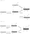
- FIG. 1 a method for manufacturing a 3C-SiC laminate substrate according to the first embodiment of the present invention is described, referring to FIG. 1 .
- FIG. 1 is a view illustrating an example of the manufacturing flow of the laminate substrate, and a view illustrating the manufacturing flow of the laminate substrate composed of a single crystal silicon substrate and a 3C-SiC.
- the inventive method for manufacturing a 3C-SiC laminate substrate includes the steps of epitaxially growing a 3C-SiC single crystal film 10 on a first single crystal silicon substrate 11, bonding a support substrate 20 on an upper surface of the 3C-SiC single crystal film, and removing the first single crystal silicon substrate 11 to manufacture a 3C-SiC laminate substrate 31.
- the first single crystal silicon substrate 11 (low-resistance substrate: resistivity is preferably 0.001 ⁇ cm or higher and less than 0.1 ⁇ cm, for example, 0.005 ⁇ cm) is placed in a reduced pressure (RP)-CVD apparatus and a native oxide film on a surface is removed by hydrogen baking (H 2 anneal).
- H 2 anneal When an oxide film remains, nucleation of SiC cannot be performed on the first single crystal silicon substrate 11.
- the H 2 anneal at this time preferably has a condition of a temperature of 1000°C or higher and 1200°C or lower. When the temperature is lower than 1000°C, a prolonged processing time is required to prevent the residual native oxide film. Conversely, the temperature exceeding 1200°C raises concerns about slip generation.
- a pressure and time for the H 2 annealing at this time are not particularly limited as long as the native oxide film is removed.
- the RP-CVD apparatus it is possible to handle a substrate having a large diameter.
- the substrate having a diameter of 200mm or larger, 450 mm or smaller is used as the first single crystal silicon substrate 11.
- the first single crystal silicon substrate 11 a substrate having a thickness of approximately 770 ⁇ m is used.
- a carbonization gas such as a propane gas or a gas containing carbon and silicon such as trimethylsilane gas is introduced as a raw material gas.
- the temperature thereof is then gradually raised from a temperature in a range of 300°C or higher and 950°C or lower to a temperature in a range of 1000°C or higher and lower than 1200°C.
- a growth rate is in a range of 0.5 to 5°C/min, and approximately 1°C/min is preferable.
- the growth may either be stopped or continued until reaching a predetermined film thickness. Alternatively, when reaching the predetermined film thickness during the temperature rise, the growth may be stopped at that point.
- a gradual increase in a film-forming rate is enabled by continuously changing a growth mode. This forms the SiC single crystal film 10.
- the support substrate 20 having the same diameter is provided, and bonding therebetween is performed.
- a second single crystal silicon substrate 12 (high-resistance substrate: a resistivity thereof is preferably 500 ⁇ cm or higher and 10000 ⁇ cm or lower, for example, larger than 1000 ⁇ cm) is bonded as the support substrate 20, at this time, a surface of the 3C-SiC substrate 10 described above may be bonded to the support substrate 20 as is, or the bonding may be performed after activating the surfaces of the respective substrates by using gases such as O 2 , N 2 , or O 3 activated by plasma.
- the bonding strength by heat treatment is further enhanced by processing at 300 to 600°C for a short time after bonding but not mandatory.
- the first single crystal silicon substrate 11 having low resistance is removed.
- Silicon having a thickness of approximately 770 ⁇ m may be completely etched using nitrohydrofluoric acid, and grinding and polishing may be combined.
- the low-resistance substrate side has a faster etching rate compared to the high-resistance substrate, only the first single crystal silicon substrate 11 is removed by etching, and the second single crystal silicon substrate 12, being the support substrate 20, is not etched away completely.
- the 3C-SiC laminate substrate 31, in which the 3C-SiC single crystal film 10 is laminated on the single crystal silicon substrate 12 and the 3C-SiC single crystal film has a diameter of 200 mm or larger, can be obtained.
- FIG. 2 is a view illustrating another example of the manufacturing flow of a laminate substrate, and a view illustrating the manufacturing flow of the laminate substrate composed of a single crystal silicon substrate, a diamond, a 3C-SiC, and a single crystal silicon substrate.
- the second embodiment has the same configuration as the first embodiment except that, a support substrate 20 in which a diamond 15 is grown on a third single crystal silicon substrate 13 is used instead of a second single crystal silicon substrate 12 as a support substrate 20, and the single crystal silicon substrate is not removed after bonding.
- the support substrate 20 having the same diameter as a first single crystal silicon substrate 11 is provided.
- the support substrate 20 is a substrate in which the diamond 15 is grown on the third single crystal silicon substrate 13.
- this substrate is formed by growing the diamond 15 on the third single crystal silicon substrate 13 by a hot-filament method.
- Bonding is performed using this support substrate 20.
- N 2 plasma is used when bonding.
- O 2 or O 3 is used, the diamond is vaporized by oxidation.
- the single crystal silicon substrate 13, the diamond 15, a 3C-SiC single crystal film 10, and the single crystal silicon substrate 11 are laminated in this order, and then a 3C-SiC laminate substrate 31 is obtained.
- the 3C-SiC single crystal film 10 preferably has a diameter of 200 mm or larger and 450 mm or smaller. Since a configuration in which the 3C-SiC single crystal film 10 on the diamond 15 with high thermal conductivity is laminated, it can be applied to a power device or a high-frequency device.
- the first single crystal silicon substrate may be removed to make a three-layer laminate substrate, depending on the purpose.
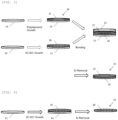
- FIG. 3 is a view illustrating a further example of the manufacturing flow of a laminate substrate, and a view illustrating the manufacturing flow of the laminate substrate composed of a diamond and a 3C-SiC.
- the third embodiment has the same configuration as the second embodiment except that a first and a third single crystal silicon substrate are removed after bonding.
- 3C-SiC laminate substrate can be obtained, in which a single crystal silicon substrate, a diamond, a 3C-SiC single crystal film, and a single crystal silicon substrate are laminated in this order, by bonding in the same configuration as in the second embodiment.
- Both single crystal silicon substrates are removed after bonding. At that time, only low-resistance silicon can be etched when nitrohydrofluoric acid is used. Consequently, by making not only a first single crystal silicon substrate 11 but also a third single crystal silicon substrate 13 into the low-resistance substrates (preferably, a resistivity is 0.001 ⁇ cm or higher and less than 0.1 ⁇ cm, for example, 0.005 ⁇ cm), then after bonding, not only the first single crystal silicon substrate 11 but also the third single crystal silicon substrate 13 can be removed.
- the 3C-SiC single crystal film 10 is laminated on the diamond 15, and then a 3C-SiC laminate substrate 31 is obtained.
- the 3C-SiC single crystal film 10 preferably has a diameter of 200 mm or larger and 450 mm or smaller. Since a configuration is composed of the 3C-SiC single crystal film 10 laminated on the diamond 15 with high thermal conductivity, it can be applied to a power device or a high-frequency device.
- FIG. 4 is a view illustrating an example of a flow diagram for manufacturing a freestanding substrate.
- a first single crystal silicon substrate 11 (low-resistance substrate: resistivity is preferably 0.001 ⁇ cm or higher and less than 0.1 ⁇ cm, for example, 0.005 ⁇ cm) is placed in a reduced pressure (RP)-CVD apparatus and a native oxide film on a surface is removed by hydrogen baking (H 2 anneal).
- H 2 anneal When an oxide film remains, nucleation of SiC cannot be performed on the first single crystal silicon substrate 11.
- the H 2 anneal at this time preferably has a condition of a temperature of 1000°C or higher and 1200°C or lower. When the temperature is lower than 1000°C, a prolonged processing time is required to prevent the residual native oxide film. Conversely, the temperature exceeding 1200°C raises concerns about slip generation.
- a pressure and time for the H 2 annealing at this time are not particularly limited as long as the native oxide film is removed.
- the RP-CVD apparatus it is possible to handle a substrate having a large diameter.
- a substrate having a diameter of 200mm or larger and 450 mm or smaller is used as the first single crystal silicon substrate 11.
- the first single crystal silicon substrate 11 a substrate having a thickness of approximately 770 ⁇ m is used.
- the temperature thereof is then gradually raised from a temperature in a range of 300°C or higher and 950°C or lower to a temperature in a range of 1000°C or higher and lower than 1200°C.
- a growth rate is in a range of 0.5 to 5°C/min, and approximately 1°C/min is preferable. At this point, after the temperature is raised to a predetermined temperature, the growth may either be stopped or continued until reaching a predetermined film thickness.
- the growth when reaching the predetermined film thickness during the temperature rise, the growth may be stopped at that point.
- a gradual increase in a film-forming rate is enabled by continuously changing a growth mode. This forms a 3C-SiC single crystal film 10.
- the first single crystal silicon substrate 11 (low-resistance substrate: resistivity is preferably 0.001 ⁇ cm or higher and less than 0.1 ⁇ cm, for example, 0.005 ⁇ cm) is removed. Silicon having a thickness of approximately 770 ⁇ m may be completely etched using nitrohydrofluoric acid, and grinding and polishing may be combined.
- a freestanding 3C-SiC substrate 32 being a substrate composed of the 3C-SiC single crystal film 10 where the 3C-SiC single crystal film has a diameter of 200 mm or larger, can be obtained.
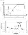
- FIG. 5 is a view illustrating an example of a growth sequence of 3C-SiC.
- 3C-SiC growths in Examples 1 and 2 were performed according to the growth sequence of 3C-SiC shown in FIG. 5 .
- a boron-doped single crystal silicon (111) substrate having low resistance (resistivity: 0.005 ⁇ cm, hereinafter also referred to as "wafer") and a diameter of 300 mm was provided.
- the wafer was placed on a susceptor in a reaction furnace of an RP-CVD apparatus and then H 2 anneal was performed at 1080°C for 1 minute.
- trimethylsilane gas was introduced while raising the temperature to 1130°C at a temperature rise rate of 1°C/sec, and nucleation of SiC and subsequent formation of a 3C-SiC single crystal film were performed.
- a growth pressure at this time was set to 100 Torr (13332.2 Pa) uniformly. After reaching 1130°C, the temperature was held for 10 minutes, and the growth of the 3C-SiC single crystal film was performed (film thickness: 200 nm).
- a boron-doped single crystal silicon (111) substrate having high resistance (resistivity: 1000 ⁇ cm) and a diameter of 300 mm was provided. Both bonding surfaces of the silicon and the 3C-SiC were irradiated with N 2 plasma (250 Torr (33330.6 Pa), N 2 : 300 sccm, RF power 100 W, 10 minutes), then bonded to each other.
- the 3C-SiC film was then confirmed by XRD in an In-plane arrangement.
- FIG. 6 is a view illustrating a result of an In-plane XRD analysis of a 3C-SiC (111) laminate substrate manufactured in Example 1.
- a boron-doped single crystal silicon (111) substrate having low resistance (resistivity: 0.005 ⁇ cm, hereinafter also referred to as "wafer") having a diameter of 300 mm was provided.
- the wafer was placed on a susceptor in a reaction furnace of an RP-CVD apparatus and then H 2 anneal was performed at 1080°C for 1 minute.
- trimethylsilane gas was introduced while raising the temperature to 1130°C at a temperature rise rate of 1°C/sec, and a nucleation step of SiC and subsequent formation of a 3C-SiC single crystal film were performed.
- a growth pressure at this time was set to 100 Torr (13332.2 Pa) uniformly. After reaching 1130°C, the temperature was held for 10 minutes, and the growth of the 3C-SiC single crystal film was performed (film thickness: 200 nm).
- a boron-doped single crystal silicon (111) substrate having low resistance (resistivity: 0.005 ⁇ cm) and a diameter of 300 mm was provided. Polydiamond was then grown thereon for 100 ⁇ m by a hot-filament CVD apparatus (5 Torr (666.612 Pa), filament temperature: 2250°C, CH 4 : 1%).
- both bonding surfaces of the silicon and the 3C-SiC were irradiated with N 2 plasma (250 Torr (33330.6 Pa), N 2 : 300 sccm, RF power 100 W, 10 minutes), then bonded to each other.
- the 3C-SiC film was then confirmed by XRD in an In-plane arrangement.
- FIG. 7 is a view illustrating a result of an In-plane XRD analysis of a 3C-SiC (111) laminate substrate manufactured in Example 2.
- the 3C-SiC laminate substrate having a large diameter and few defects was successfully manufactured in an easy and reliable manner.
- the present description includes the following embodiments.
Landscapes
- Chemical & Material Sciences (AREA)
- Engineering & Computer Science (AREA)
- Crystallography & Structural Chemistry (AREA)
- Materials Engineering (AREA)
- Metallurgy (AREA)
- Organic Chemistry (AREA)
- Chemical Kinetics & Catalysis (AREA)
- General Chemical & Material Sciences (AREA)
- Inorganic Chemistry (AREA)
- Crystals, And After-Treatments Of Crystals (AREA)
- Recrystallisation Techniques (AREA)
Abstract
The present invention is a method for manufacturing a 3C-SiC laminate substrate, the method includes the steps of epitaxially growing a 3C-SiC single crystal film on a first single crystal silicon substrate, bonding a support substrate on an upper surface of the 3C-SiC single crystal film, and removing the first single crystal silicon substrate to manufacture the 3C-SiC laminate substrate. Therefore, an object is to provide a method for manufacturing a 3C-SiC laminate substrate. In particular, this provides a method for obtaining a 3C-SiC laminate substrate having a large diameter such as 200 mmϕ or 300 mmϕ.
Description
- The present invention relates to a method for manufacturing a 3C-SiC laminate substrate, a 3C-SiC laminate substrate, and a freestanding 3C-SiC substrate.
- SiC has a wide bandgap of 2.2 to 3.3 eV which gives a high dielectric breakdown strength and high thermal conductivity, making it a promising material as a semiconductor material for various semiconductor devices such as power devices and high-frequency devices. In addition, although SiC is known for having different crystal structures such as 3C, 4H, and 6H, 3C is a cubic crystal and is known as a promising material for devices in which orientation dependence is absent.
- With such a background, 3C-SiC growth has been studied for a long time, where bulk growth (see,
Non Patent Documents 1 and 2), and heteroepitaxial growth (Non Patent Document 3 discloses early heteroepitaxial growth, andPatent Documents 1 to 5 disclose recent heteroepitaxial growth on a silicon substrate) are known. When summarizing these previous researches and patents, (1) high-temperature (higher than 1500°C) is required for the bulk growth, resulting in great difficulty in enlarging a diameter applicable to devices, (2) on the other hand, high-temperature as in 4H or 6H (higher than 1500°C) is not required in epitaxial growth, enabling the growth approximately at a temperature of 1100°C, thus the growth on the silicon substrate is also possible which is advantageous in terms of enlarging the diameter. - Based on these findings, research has been conducted for heteroepitaxially growing 3C-SiC and leaving only 3C-SiC epitaxial film (Non Patent Document 4). In this method, a 2-inch freestanding 3C-SiC substrate is manufactured by growing approximately 100 µm of 3C-SiC on a Si (111) substrate and then removing Si using nitrohydrofluoric acid.
- In order to realize this method in large-diameter substrates, it is necessary to grow thick SiC. When considering defect generation due to the difference in lattice constant and the difference in coefficient of linear expansion, thick film forming on Si is accompanied with difficulty and only small-diameter substrates such as 4H and 6H can likely be obtained.
-
- Patent Document 1:
JP 2018-522412 A - Patent Document 2:
JP 2021-20819 A - Patent Document 3:
JP 2006-253617 A - Patent Document 4:
JP 2008-184361 A - Patent Document 5:
JP 2017-39622 A -
- Non Patent Document 1: H.Nagasawa, K.Yagi and T.Kawahara: J.Cryst.Growth, 239 (2002) 1244.
- Non Patent Document 2: D.Chaussende, F.Mercier, A.Boulle, F.Conchon, M.Soueidan, G.Ferro, A.Mantzari, A.Andreadou, E.K.Polychroniadis, C.Balloud, S.Juillaguet, J.Camassel and M.Pons: J.Cryst.Growth, 310 (2008) 976.
- Non Patent Document 3: T.Ujihara, R.Maekawa, R.Tanaka, K.Sasaki, K.Kuroda and Y.Takeda: J.Cryst.Growth, 310 (2008) 1438.
- Non Patent Document 4: "Crystal Quality of Free-Standing 3C-SiC (111) Substrates by Low Temperature Growth", the 62nd JSAP Spring Meeting 2015, Extended Abstracts, 13-095 (2015).
- The present invention has been made to solve the above-described problem. An object of the present invention is to provide a method for manufacturing a 3C-SiC laminate substrate. In particular, an object is to provide a method for obtaining a 3C-SiC laminate substrate having a large diameter such as a diameter of 200 mm or 300 mm. Moreover, an object is to obtain a 3C-SiC laminate substrate or a freestanding 3C-SiC substrate.
- The present invention has been made to achieve the above objects and provide a method for manufacturing a 3C-SiC laminate substrate, the method comprising the steps of:
- epitaxially growing a 3C-SiC single crystal film on a first single crystal silicon substrate;
- bonding a support substrate on an upper surface of the 3C-SiC single crystal film; and
- removing the first single crystal silicon substrate to manufacture the 3C-SiC laminate substrate.
- According to such a method for manufacturing a 3C-SiC laminate substrate, the 3C-SiC laminate substrate, in particular, the 3C-SiC laminate substrate having a large diameter and few defects can be easily and reliably manufactured. This enables to decrease a manufacture cost.
- According to such a method, it is possible to manufacture the 3C-SiC laminate substrate with a thin epitaxial film that has few defects, without the need for growing thick SiC. The epitaxially grown substrate is bonded to a support substrate and a first silicon substrate is then delaminated. This releases the epitaxial film from the lattice mismatch of the substrate, reducing the likelihood of defect generation in the 3C-SiC single crystal film.
- According to such a method, the manufacture of the 3C-SiC laminate substrate having a large diameter of 200 mm or even 300 mm or larger is enabled by using a silicon substrate having a diameter of 200 mm or larger.
- In addition, various substrates are envisaged as the support substrates. A sintered body or polycrystal of SiC, or ceramic is sufficient, and sapphire is sufficient. When considering the low cost and ease of processing, the use of the single crystal silicon substrate is the most suitable.
- In particular, when a low-resistance substrate having a high concentration of boron or dopant is used as a substrate for an initial 3C-SiC epitaxial growth, and a high-resistance substrate having a low concentration of boron and dopant is used for the support substrate on the 3C-SiC epitaxial side, the high-resistance substrate is barely etched during nitrohydrofluoric acid etching. On the other hand, the low-resistance substrate has a higher etching rate, enabling thereof to ensure selectivity to remove the low-resistance substrate while retaining the high-resistance substrate. This facilitates the manufacturing of the 3C-SiC laminate substrate.
- In this case, the first single crystal silicon substrate can have a resistivity of less than 0.1 Ω·cm.
- In this way, when the high-resistance substrate having a low concentration of boron or dopant is used for the support substrate on the 3C-SiC epitaxial side, the high-resistance substrate is barely etched during nitrohydrofluoric acid etching. On the other hand, the low-resistance substrate has a higher etching rate, enabling thereof to ensure selectivity to remove the low-resistance substrate being the first single crystal silicon substrate while retaining the high-resistance substrate being the support substrate. As a result, the 3C-SiC laminate substrate can be manufactured.
- In this case, the method for manufacturing a 3C-SiC laminate substrate described above is provided, wherein
the support substrate is either a second single crystal silicon substrate or a substrate in which a diamond is grown on a third single crystal silicon substrate. - Accordingly, the 3C-SiC laminate substrate in which the 3C-SiC single crystal film is laminated on the single crystal silicon substrate and the 3C-SiC single crystal film has a diameter of 200 mm or larger, or the 3C-SiC laminate substrate in which the 3C-SiC single crystal film is laminated on the diamond, can be obtained.
- In this case, the method for manufacturing a 3C-SiC laminate substrate described above is provided, wherein
the second single crystal silicon substrate has a resistivity of 500 Ω·cm or higher. - In this way, the high-resistance substrate is barely etched during nitrohydrofluoric acid etching. On the other hand, the low-resistance substrate has a higher etching rate, enabling thereof to ensure selectivity to remove the low-resistance substrate being the first single crystal silicon substrate while retaining the high-resistance substrate being the second single crystal silicon substrate. As a result, the 3C-SiC laminate substrate, in which the 3C-SiC single crystal film is laminated on the single crystal silicon substrate, and the 3C-SiC single crystal film has a diameter of 200 mm or larger, can be obtained.
- In this case, the method for manufacturing a 3C-SiC laminate substrate described above is provided, wherein
the third single crystal silicon substrate has a resistivity of less than 0.1 Ω·cm. - This allows, after bonding, the removal of the third single crystal silicon substrate during silicon removal while retaining the diamond,
and obtaining the 3C-SiC laminate substrate in which the 3C-SiC single crystal film is laminated on the diamond. - In this case, the method for manufacturing a 3C-SiC laminate substrate described above is provided, wherein
in a case where the substrate in which the diamond is grown on the third single crystal silicon substrate is used as the support substrate, when the first single crystal silicon substrate is removed, the third single crystal silicon substrate is also removed and the diamond is left, thereby manufacturing the 3C-SiC laminate substrate. - In this way, the 3C-SiC laminate substrate in which the 3C-SiC single crystal film is laminated on the diamond can be efficiently obtained.
- In this case, the method for manufacturing a 3C-SiC laminate substrate described above is provided, wherein
the 3C-SiC single crystal film has a diameter of 200 mm or larger. - According to the present invention, the 3C-SiC laminate substrate having such a large diameter can be obtained while also reducing the manufacturing cost.
- The present invention provides a 3C-SiC laminate substrate, wherein
- a 3C-SiC single crystal film is laminated on a single crystal silicon substrate, and
- the 3C-SiC single crystal film has a diameter of 200 mm or larger.
- With the 3C-SiC laminate substrate having such a large diameter, manufacturing cost can be reduced.
- The present invention provides a 3C-SiC laminate substrate, wherein
a 3C-SiC single crystal film is laminated on a diamond. - According to such a 3C-SiC laminate substrate, manufacturing cost can be reduced. In particular, it is applicable for a power device and a high-frequency device utilizing an excellent heat-dissipating property of diamond.
- The present invention provides a 3C-SiC laminate substrate, wherein
a single crystal silicon substrate, a diamond, a 3C-SiC single crystal film, and a single crystal silicon substrate are laminated in this order. - According to such a 3C-SiC laminate substrate, manufacturing cost can be reliably reduced. In particular, it is applicable for a power device and a high-frequency device utilizing an excellent heat-dissipating property of diamond.
- The present invention provides the 3C-SiC laminate substrate described above, wherein
the 3C-SiC single crystal film has a diameter of 200 mm or larger. - According to such a 3C-SiC laminate substrate, manufacturing cost can be more reliably reduced.
- The present invention provides a freestanding 3C-SiC substrate, the freestanding 3C-SiC substrate being a substrate comprising a 3C-SiC single crystal film, wherein
the 3C-SiC single crystal film has a diameter of 200 mm or larger. - In the present invention, the freestanding 3C-SiC substrate having such a large diameter can be obtained. Therefore, it can be expected to find applications for various devices.
- As described above, according to the inventive method for manufacturing a 3C-SiC laminate substrate, the 3C-SiC laminate substrate, in particular, the 3C-SiC laminate substrate having a large diameter and few defects can be easily and reliably manufactured.
- According to the inventive 3C-SiC laminate substrate, manufacturing cost can be reduced.
- According to a configuration of the present invention, a large-diameter freestanding 3C-SiC substrate can be obtained through a simple manufacturing process.
-
-
FIG. 1 is a view illustrating an example of a manufacturing flow of a laminate substrate, and a view illustrating a manufacturing flow of a laminate substrate composed of a single crystal silicon substrate and a 3C-SiC. -
FIG. 2 is a view illustrating another example of a manufacturing flow of a laminate substrate, and a view illustrating a manufacturing flow of a laminate substrate composed of a single crystal silicon substrate, a diamond, a 3C-SiC, and a single crystal silicon substrate. -
FIG. 3 is a view illustrating a further example of a manufacturing flow of a laminate substrate, and a view illustrating a manufacturing flow of a laminate substrate composed of a diamond and a 3C-SiC. -
FIG. 4 is a view illustrating an example of a flow diagram for manufacturing a freestanding substrate. -
FIG. 5 is a view illustrating an example of a growth sequence of 3C-SiC. -
FIG. 6 is a view illustrating a result of an In-plane XRD analysis of a 3C-SiC (111) laminate substrate manufactured in Example 1. -
FIG. 7 is a view illustrating a result of an In-plane XRD analysis of a 3C-SiC (111) laminate substrate manufactured in Example 2. - Hereinafter, the present invention will be described in detail. However, the present invention is not limited thereto.
- As described above, a method for manufacturing a 3C-SiC laminate substrate, in particular, a method for obtaining a 3C-SiC laminate substrate having a large diameter such as 200 mmϕ or 300 mmϕ, and a method for obtaining a 3C-SiC laminate substrate or a freestanding 3C-SiC substrate have been required.
- To solve the above problems, the present inventors have earnestly studied and found out that a 3C-SiC laminate substrate, in particular, a 3C-SiC laminate substrate having a large diameter with few defects can be easily and reliably manufactured by a method for manufacturing a 3C-SiC laminate substrate. This method for manufacturing a 3C-SiC laminate substrate includes the steps of epitaxially growing a 3C-SiC single crystal film on a first single crystal silicon substrate, bonding a support substrate on an upper surface of the 3C-SiC single crystal film, and removing the first single crystal silicon substrate to manufacture the 3C-SiC laminate substrate. Based on this finding, the present invention has been completed.
- Hereinafter a method for manufacturing a 3C-SiC laminate substrate according to the first embodiment of the present invention is described, referring to
FIG. 1 . -
FIG. 1 is a view illustrating an example of the manufacturing flow of the laminate substrate, and a view illustrating the manufacturing flow of the laminate substrate composed of a single crystal silicon substrate and a 3C-SiC. - The inventive method for manufacturing a 3C-SiC laminate substrate includes the steps of epitaxially growing a 3C-SiC
single crystal film 10 on a first singlecrystal silicon substrate 11, bonding asupport substrate 20 on an upper surface of the 3C-SiC single crystal film, and removing the first singlecrystal silicon substrate 11 to manufacture a 3C-SiC laminate substrate 31. - First, the first single crystal silicon substrate 11 (low-resistance substrate: resistivity is preferably 0.001 Ω·cm or higher and less than 0.1 Ω·cm, for example, 0.005 Ω·cm) is placed in a reduced pressure (RP)-CVD apparatus and a native oxide film on a surface is removed by hydrogen baking (H2 anneal). When an oxide film remains, nucleation of SiC cannot be performed on the first single
crystal silicon substrate 11. The H2 anneal at this time preferably has a condition of a temperature of 1000°C or higher and 1200°C or lower. When the temperature is lower than 1000°C, a prolonged processing time is required to prevent the residual native oxide film. Conversely, the temperature exceeding 1200°C raises concerns about slip generation. A pressure and time for the H2 annealing at this time are not particularly limited as long as the native oxide film is removed. - In addition, by using the RP-CVD apparatus, it is possible to handle a substrate having a large diameter. In this case, as the first single
crystal silicon substrate 11, the substrate having a diameter of 200mm or larger, 450 mm or smaller is used. - Moreover, as the first single
crystal silicon substrate 11, a substrate having a thickness of approximately 770 µm is used. - Next, in order to form SiC nuclei on the surface of the first single
crystal silicon substrate 11 and subsequently form the 3C-SiC single crystal film, a carbonization gas such as a propane gas or a gas containing carbon and silicon such as trimethylsilane gas is introduced as a raw material gas. The temperature thereof is then gradually raised from a temperature in a range of 300°C or higher and 950°C or lower to a temperature in a range of 1000°C or higher and lower than 1200°C. A growth rate is in a range of 0.5 to 5°C/min, and approximately 1°C/min is preferable. At this point, after the temperature is raised to a predetermined temperature, the growth may either be stopped or continued until reaching a predetermined film thickness. Alternatively, when reaching the predetermined film thickness during the temperature rise, the growth may be stopped at that point. By growing with changing the temperature, a gradual increase in a film-forming rate is enabled by continuously changing a growth mode. This forms the SiCsingle crystal film 10. - Next, the
support substrate 20 having the same diameter is provided, and bonding therebetween is performed. While a second single crystal silicon substrate 12 (high-resistance substrate: a resistivity thereof is preferably 500 Ω·cm or higher and 10000 Ω·cm or lower, for example, larger than 1000 Ω·cm) is bonded as thesupport substrate 20, at this time, a surface of the 3C-SiC substrate 10 described above may be bonded to thesupport substrate 20 as is, or the bonding may be performed after activating the surfaces of the respective substrates by using gases such as O2, N2, or O3 activated by plasma. The bonding strength by heat treatment is further enhanced by processing at 300 to 600°C for a short time after bonding but not mandatory. - Finally, the first single
crystal silicon substrate 11 having low resistance is removed. Silicon having a thickness of approximately 770 µm may be completely etched using nitrohydrofluoric acid, and grinding and polishing may be combined. In the etching using nitrohydrofluoric acid, the low-resistance substrate side has a faster etching rate compared to the high-resistance substrate, only the first singlecrystal silicon substrate 11 is removed by etching, and the second singlecrystal silicon substrate 12, being thesupport substrate 20, is not etched away completely. - According to the above steps, the 3C-
SiC laminate substrate 31, in which the 3C-SiCsingle crystal film 10 is laminated on the singlecrystal silicon substrate 12 and the 3C-SiC single crystal film has a diameter of 200 mm or larger, can be obtained. -
FIG. 2 is a view illustrating another example of the manufacturing flow of a laminate substrate, and a view illustrating the manufacturing flow of the laminate substrate composed of a single crystal silicon substrate, a diamond, a 3C-SiC, and a single crystal silicon substrate. - The second embodiment has the same configuration as the first embodiment except that, a
support substrate 20 in which adiamond 15 is grown on a third singlecrystal silicon substrate 13 is used instead of a second singlecrystal silicon substrate 12 as asupport substrate 20, and the single crystal silicon substrate is not removed after bonding. - The
support substrate 20 having the same diameter as a first singlecrystal silicon substrate 11 is provided. Thesupport substrate 20 is a substrate in which thediamond 15 is grown on the third singlecrystal silicon substrate 13. For example, this substrate is formed by growing thediamond 15 on the third singlecrystal silicon substrate 13 by a hot-filament method. - Bonding is performed using this
support substrate 20. N2 plasma is used when bonding. When O2 or O3 is used, the diamond is vaporized by oxidation. - By the above steps, the single
crystal silicon substrate 13, thediamond 15, a 3C-SiCsingle crystal film 10, and the singlecrystal silicon substrate 11 are laminated in this order, and then a 3C-SiC laminate substrate 31 is obtained. The 3C-SiCsingle crystal film 10 preferably has a diameter of 200 mm or larger and 450 mm or smaller. Since a configuration in which the 3C-SiCsingle crystal film 10 on thediamond 15 with high thermal conductivity is laminated, it can be applied to a power device or a high-frequency device. - It is needless to say the first single crystal silicon substrate may be removed to make a three-layer laminate substrate, depending on the purpose.
-
FIG. 3 is a view illustrating a further example of the manufacturing flow of a laminate substrate, and a view illustrating the manufacturing flow of the laminate substrate composed of a diamond and a 3C-SiC. - The third embodiment has the same configuration as the second embodiment except that a first and a third single crystal silicon substrate are removed after bonding.
- 3C-SiC laminate substrate can be obtained, in which a single crystal silicon substrate, a diamond, a 3C-SiC single crystal film, and a single crystal silicon substrate are laminated in this order, by bonding in the same configuration as in the second embodiment.
- Both single crystal silicon substrates are removed after bonding. At that time, only low-resistance silicon can be etched when nitrohydrofluoric acid is used. Consequently, by making not only a first single
crystal silicon substrate 11 but also a third singlecrystal silicon substrate 13 into the low-resistance substrates (preferably, a resistivity is 0.001 Ω·cm or higher and less than 0.1 Ω·cm, for example, 0.005 Ω·cm), then after bonding, not only the first singlecrystal silicon substrate 11 but also the third singlecrystal silicon substrate 13 can be removed. - By the above steps, the 3C-SiC
single crystal film 10 is laminated on thediamond 15, and then a 3C-SiC laminate substrate 31 is obtained. The 3C-SiCsingle crystal film 10 preferably has a diameter of 200 mm or larger and 450 mm or smaller. Since a configuration is composed of the 3C-SiCsingle crystal film 10 laminated on thediamond 15 with high thermal conductivity, it can be applied to a power device or a high-frequency device. -
FIG. 4 is a view illustrating an example of a flow diagram for manufacturing a freestanding substrate. - First, a first single crystal silicon substrate 11 (low-resistance substrate: resistivity is preferably 0.001 Ω·cm or higher and less than 0.1 Ω·cm, for example, 0.005 Ω·cm) is placed in a reduced pressure (RP)-CVD apparatus and a native oxide film on a surface is removed by hydrogen baking (H2 anneal). When an oxide film remains, nucleation of SiC cannot be performed on the first single
crystal silicon substrate 11. The H2 anneal at this time preferably has a condition of a temperature of 1000°C or higher and 1200°C or lower. When the temperature is lower than 1000°C, a prolonged processing time is required to prevent the residual native oxide film. Conversely, the temperature exceeding 1200°C raises concerns about slip generation. A pressure and time for the H2 annealing at this time are not particularly limited as long as the native oxide film is removed. - In addition, by using the RP-CVD apparatus, it is possible to handle a substrate having a large diameter. In this case, as the first single
crystal silicon substrate 11, a substrate having a diameter of 200mm or larger and 450 mm or smaller is used. - Moreover, as the first single
crystal silicon substrate 11, a substrate having a thickness of approximately 770 µm is used. - Next, in order to form SiC nuclei on the surface of the first single
crystal silicon substrate 11 and subsequently form a 3C-SiC single crystal film, while a carbonization gas such as propane gas is introduced as a raw material gas, the temperature thereof is then gradually raised from a temperature in a range of 300°C or higher and 950°C or lower to a temperature in a range of 1000°C or higher and lower than 1200°C. A growth rate is in a range of 0.5 to 5°C/min, and approximately 1°C/min is preferable. At this point, after the temperature is raised to a predetermined temperature, the growth may either be stopped or continued until reaching a predetermined film thickness. Alternatively, when reaching the predetermined film thickness during the temperature rise, the growth may be stopped at that point. By growing with changing the temperature, a gradual increase in a film-forming rate is enabled by continuously changing a growth mode. This forms a 3C-SiCsingle crystal film 10. - Finally, the first single crystal silicon substrate 11 (low-resistance substrate: resistivity is preferably 0.001 Ω·cm or higher and less than 0.1 Ω·cm, for example, 0.005 Ω·cm) is removed. Silicon having a thickness of approximately 770 µm may be completely etched using nitrohydrofluoric acid, and grinding and polishing may be combined.
- With the above steps, a freestanding 3C-
SiC substrate 32, being a substrate composed of the 3C-SiCsingle crystal film 10 where the 3C-SiC single crystal film has a diameter of 200 mm or larger, can be obtained. - Hereinafter, the present invention will be specifically described with reference to Examples. However, the present invention is not limited thereto.
-
FIG. 5 is a view illustrating an example of a growth sequence of 3C-SiC. 3C-SiC growths in Examples 1 and 2 were performed according to the growth sequence of 3C-SiC shown inFIG. 5 . - First, a boron-doped single crystal silicon (111) substrate having low resistance (resistivity: 0.005 Ω·cm, hereinafter also referred to as "wafer") and a diameter of 300 mm was provided. The wafer was placed on a susceptor in a reaction furnace of an RP-CVD apparatus and then H2 anneal was performed at 1080°C for 1 minute.
- Subsequently, after lowering the temperature in the furnace to 300°C, trimethylsilane gas was introduced while raising the temperature to 1130°C at a temperature rise rate of 1°C/sec, and nucleation of SiC and subsequent formation of a 3C-SiC single crystal film were performed. A growth pressure at this time was set to 100 Torr (13332.2 Pa) uniformly. After reaching 1130°C, the temperature was held for 10 minutes, and the growth of the 3C-SiC single crystal film was performed (film thickness: 200 nm).
- After film-forming, a boron-doped single crystal silicon (111) substrate having high resistance (resistivity: 1000 Ω·cm) and a diameter of 300 mm was provided. Both bonding surfaces of the silicon and the 3C-SiC were irradiated with N2 plasma (250 Torr (33330.6 Pa), N2: 300 sccm,
RF power 100 W, 10 minutes), then bonded to each other. - Subsequently, the single crystal silicon substrate on the low-resistance side was removed by immersion in a nitrohydrofluoric acid solution (H2O: HF: HNO3=5: 1: 1).
- The 3C-SiC film was then confirmed by XRD in an In-plane arrangement.
-
FIG. 6 is a view illustrating a result of an In-plane XRD analysis of a 3C-SiC (111) laminate substrate manufactured in Example 1. - As shown in
FIG. 6 , a peak of 3C-SiC(220) parallel to Si(220) was successfully confirmed, and the growth of the 3C-SiC film of a single crystal was confirmed. - First, a boron-doped single crystal silicon (111) substrate having low resistance (resistivity: 0.005 Ω·cm, hereinafter also referred to as "wafer") having a diameter of 300 mm was provided. The wafer was placed on a susceptor in a reaction furnace of an RP-CVD apparatus and then H2 anneal was performed at 1080°C for 1 minute.
- Subsequently, after lowering the temperature in the furnace to 300°C, trimethylsilane gas was introduced while raising the temperature to 1130°C at a temperature rise rate of 1°C/sec, and a nucleation step of SiC and subsequent formation of a 3C-SiC single crystal film were performed. A growth pressure at this time was set to 100 Torr (13332.2 Pa) uniformly. After reaching 1130°C, the temperature was held for 10 minutes, and the growth of the 3C-SiC single crystal film was performed (film thickness: 200 nm).
- On the other hand, a boron-doped single crystal silicon (111) substrate having low resistance (resistivity: 0.005 Ω·cm) and a diameter of 300 mm was provided. Polydiamond was then grown thereon for 100 µm by a hot-filament CVD apparatus (5 Torr (666.612 Pa), filament temperature: 2250°C, CH4: 1%).
- Next, both bonding surfaces of the silicon and the 3C-SiC were irradiated with N2 plasma (250 Torr (33330.6 Pa), N2: 300 sccm,
RF power 100 W, 10 minutes), then bonded to each other. - Subsequently, all of the single crystal silicon substrates having low resistance were removed by immersion in a nitrohydrofluoric acid solution (H2O: HF: HNO3=5: 1: 1).
- The 3C-SiC film was then confirmed by XRD in an In-plane arrangement.
-
FIG. 7 is a view illustrating a result of an In-plane XRD analysis of a 3C-SiC (111) laminate substrate manufactured in Example 2. - As shown in
FIG. 7 , a peak of 3C-SiC(220) parallel to Si(220) was successfully confirmed, and the growth of the 3C-SiC film of a single crystal was confirmed. - As described above, according to Examples of the present invention, the 3C-SiC laminate substrate having a large diameter and few defects was successfully manufactured in an easy and reliable manner.
- The present description includes the following embodiments.
- [1]: A method for manufacturing a 3C-SiC laminate substrate, the method comprising the steps of:
- epitaxially growing a 3C-SiC single crystal film on a first single crystal silicon substrate;
- bonding a support substrate on an upper surface of the 3C-SiC single crystal film; and
- removing the first single crystal silicon substrate to manufacture the 3C-SiC laminate substrate.
- [2]: The method for manufacturing a 3C-SiC laminate substrate according to the above [1], wherein
the first single crystal silicon substrate has a resistivity of less than 0.1 Ω·cm. - [3]: The method for manufacturing a 3C-SiC laminate substrate according to the above [1] or [2], wherein
the support substrate is either a second single crystal silicon substrate or a substrate in which a diamond is grown on a third single crystal silicon substrate. - [4]: The method for manufacturing a 3C-SiC laminate substrate according to the above [3], wherein
the second single crystal silicon substrate has a resistivity of 500 Ω·cm or higher. - [5]: The method for manufacturing a 3C-SiC laminate substrate according to the above [3], wherein
the third single crystal silicon substrate has a resistivity of less than 0.1 Ω·cm. - [6]: The method for manufacturing a 3C-SiC laminate substrate according to the above [3] or [5], wherein
in a case where the substrate in which the diamond is grown on the third single crystal silicon substrate is used as the support substrate, when the first single crystal silicon substrate is removed, the third single crystal silicon substrate is also removed and the diamond is left, thereby manufacturing the 3C-SiC laminate substrate. - [7]: The method for manufacturing a 3C-SiC laminate substrate according to any one of the above [1] to [6], wherein
the 3C-SiC single crystal film has a diameter of 200 mm or larger. - [8]: A 3C-SiC laminate substrate, wherein
- a 3C-SiC single crystal film is laminated on a single crystal silicon substrate, and
- the 3C-SiC single crystal film has a diameter of 200 mm or larger.
- [9]: A 3C-SiC laminate substrate, wherein
a 3C-SiC single crystal film is laminated on a diamond. - [10]: A 3C-SiC laminate substrate, wherein
a single crystal silicon substrate, a diamond, a 3C-SiC single crystal film, and a single crystal silicon substrate are laminated in this order. - [11]: The 3C-SiC laminate substrate according to
claim 9 or 10, wherein
the 3C-SiC single crystal film has a diameter of 200 mm or larger. - [12]: A freestanding 3C-SiC substrate, the freestanding 3C-SiC substrate being a substrate comprising a 3C-SiC single crystal film, wherein
the 3C-SiC single crystal film has a diameter of 200 mm or larger. - It should be noted that the present invention is not limited to the above-described embodiments. The embodiments are just examples, and any examples that have substantially the same feature and demonstrate the same functions and effects as those in the technical concept disclosed in claims of the present invention are included in the technical scope of the present invention.
Claims (12)
- A method for manufacturing a 3C-SiC laminate substrate, the method comprising the steps of:epitaxially growing a 3C-SiC single crystal film on a first single crystal silicon substrate;bonding a support substrate on an upper surface of the 3C-SiC single crystal film; andremoving the first single crystal silicon substrate to manufacture the 3C-SiC laminate substrate.
- The method for manufacturing a 3C-SiC laminate substrate according to claim 1, wherein
the first single crystal silicon substrate has a resistivity of less than 0.1 Ω·cm. - The method for manufacturing a 3C-SiC laminate substrate according to claim 1, wherein
the support substrate is either a second single crystal silicon substrate or a substrate in which a diamond is grown on a third single crystal silicon substrate. - The method for manufacturing a 3C-SiC laminate substrate according to claim 3, wherein
the second single crystal silicon substrate has a resistivity of 500 Ω·cm or higher. - The method for manufacturing a 3C-SiC laminate substrate according to claim 3, wherein
the third single crystal silicon substrate has a resistivity of less than 0.1 Ω·cm. - The method for manufacturing a 3C-SiC laminate substrate according to claim 3, wherein
in a case where the substrate in which the diamond is grown on the third single crystal silicon substrate is used as the support substrate, when the first single crystal silicon substrate is removed, the third single crystal silicon substrate is also removed and the diamond is left, thereby manufacturing the 3C-SiC laminate substrate. - The method for manufacturing a 3C-SiC laminate substrate according to claim 1, wherein
the 3C-SiC single crystal film has a diameter of 200 mm or larger. - A 3C-SiC laminate substrate, whereina 3C-SiC single crystal film is laminated on a single crystal silicon substrate, andthe 3C-SiC single crystal film has a diameter of 200 mm or larger.
- A 3C-SiC laminate substrate, wherein
a 3C-SiC single crystal film is laminated on a diamond. - A 3C-SiC laminate substrate, wherein
a single crystal silicon substrate, a diamond, a 3C-SiC single crystal film, and a single crystal silicon substrate are laminated in this order. - The 3C-SiC laminate substrate according to claim 9 or 10, wherein
the 3C-SiC single crystal film has a diameter of 200 mm or larger. - A freestanding 3C-SiC substrate, the freestanding 3C-SiC substrate being a substrate comprising a 3C-SiC single crystal film, wherein
the 3C-SiC single crystal film has a diameter of 200 mm or larger.
Applications Claiming Priority (2)
| Application Number | Priority Date | Filing Date | Title |
|---|---|---|---|
| JP2022124317 | 2022-08-03 | ||
| PCT/JP2023/022801 WO2024029217A1 (en) | 2022-08-03 | 2023-06-20 | Method for manufacturing 3c-sic laminated substrate, 3c-sic laminated substrate, and 3c-sic independent substrate |
Publications (1)
| Publication Number | Publication Date |
|---|---|
| EP4567165A1 true EP4567165A1 (en) | 2025-06-11 |
Family
ID=89848812
Family Applications (1)
| Application Number | Title | Priority Date | Filing Date |
|---|---|---|---|
| EP23849777.0A Pending EP4567165A1 (en) | 2022-08-03 | 2023-06-20 | Method for manufacturing 3c-sic laminated substrate, 3c-sic laminated substrate, and 3c-sic independent substrate |
Country Status (6)
| Country | Link |
|---|---|
| EP (1) | EP4567165A1 (en) |
| JP (1) | JPWO2024029217A1 (en) |
| KR (1) | KR20250044274A (en) |
| CN (1) | CN119677900A (en) |
| TW (1) | TW202408802A (en) |
| WO (1) | WO2024029217A1 (en) |
Family Cites Families (10)
| Publication number | Priority date | Publication date | Assignee | Title |
|---|---|---|---|---|
| JPS53146300A (en) * | 1977-05-25 | 1978-12-20 | Sharp Corp | Production of silicon carbide substrate |
| JPH10324599A (en) * | 1997-05-20 | 1998-12-08 | Denso Corp | Method for producing silicon carbide single crystal |
| JPH11268995A (en) * | 1998-03-20 | 1999-10-05 | Denso Corp | Method for producing silicon carbide single crystal |
| CN100433257C (en) * | 2004-01-15 | 2008-11-12 | 野田优 | Method for manufacturing single crystal thin film |
| JP2006253617A (en) | 2005-02-14 | 2006-09-21 | Toshiba Ceramics Co Ltd | SiC semiconductor and manufacturing method thereof |
| JP2008184361A (en) | 2007-01-30 | 2008-08-14 | Covalent Materials Corp | Method for forming 3C-SiC single crystal film |
| WO2017013445A1 (en) | 2015-07-23 | 2017-01-26 | The University Of Warwick | Growing expitaxial 3c-sic on single-crystal silicon |
| JP6450282B2 (en) | 2015-08-19 | 2019-01-09 | エア・ウォーター株式会社 | Compound semiconductor substrate and method of manufacturing compound semiconductor substrate |
| JP7259615B2 (en) | 2019-07-24 | 2023-04-18 | 株式会社Sumco | Manufacturing method of heteroepitaxial wafer |
| CN120637219A (en) * | 2020-04-03 | 2025-09-12 | 三菱电机株式会社 | Polishing method and method for manufacturing semiconductor substrate |
-
2023
- 2023-06-20 CN CN202380055877.8A patent/CN119677900A/en active Pending
- 2023-06-20 JP JP2024538853A patent/JPWO2024029217A1/ja active Pending
- 2023-06-20 EP EP23849777.0A patent/EP4567165A1/en active Pending
- 2023-06-20 WO PCT/JP2023/022801 patent/WO2024029217A1/en not_active Ceased
- 2023-06-20 KR KR1020257003058A patent/KR20250044274A/en active Pending
- 2023-06-28 TW TW112124030A patent/TW202408802A/en unknown
Also Published As
| Publication number | Publication date |
|---|---|
| CN119677900A (en) | 2025-03-21 |
| KR20250044274A (en) | 2025-03-31 |
| JPWO2024029217A1 (en) | 2024-02-08 |
| TW202408802A (en) | 2024-03-01 |
| WO2024029217A1 (en) | 2024-02-08 |
Similar Documents
| Publication | Publication Date | Title |
|---|---|---|
| TWI313892B (en) | Low 1c screw dislocation 3 inch silicon carbide wafer | |
| JP5693946B2 (en) | Method for producing single crystal 3C-SiC substrate | |
| EP3351660B1 (en) | Manufacturing method of sic composite substrate | |
| JP6631517B2 (en) | Diamond substrate and diamond composite substrate | |
| EP3352197B1 (en) | Method for producing a composite sic substrate | |
| CN121519022A (en) | Diamond substrate and its manufacturing method | |
| KR20120001606A (en) | Substrate for Single Crystal Diamond Growth and Method of Manufacturing Single Crystal Diamond Substrate | |
| CN102465343A (en) | Method of manufacturing gan-based film | |
| JP4946264B2 (en) | Method for manufacturing silicon carbide semiconductor epitaxial substrate | |
| CN104867818B (en) | A kind of method for reducing silicon carbide epitaxy material defect | |
| CN102465342B (en) | Method of manufacturing gan-based film | |
| JP7259906B2 (en) | Manufacturing method of heteroepitaxial wafer | |
| JP2010034330A (en) | Epitaxial wafer and method of manufacturing the same | |
| JP6927429B2 (en) | Manufacturing method of SiC epitaxial substrate | |
| EP4653588A1 (en) | Method for manufacturing 3c-sic single-crystal epitaxial substrate, method for manufacturing 3c-sic free-standing substrate, and 3c-sic single-crystal epitaxial substrate | |
| JP5135545B2 (en) | Seed crystal for growing silicon carbide single crystal ingot and method for producing the same | |
| JP2006253617A (en) | SiC semiconductor and manufacturing method thereof | |
| JP7218832B1 (en) | Manufacturing method of heteroepitaxial wafer | |
| CN102017080A (en) | Method for producing Si(1-v-w-x)CwAlxNv substrate, method for producing epitaxial wafer, Si(1-v-w-x)CwAlxNv substrate, and epitaxial wafer | |
| WO2024029217A1 (en) | Method for manufacturing 3c-sic laminated substrate, 3c-sic laminated substrate, and 3c-sic independent substrate | |
| CN102016135A (en) | Method for producing Si(1-v-w-x)CwAlxNv substrate, method for producing epitaxial wafer, Si(1-v-w-x)CwAlxNv substrate, and epitaxial wafer | |
| TW202332044A (en) | Process for the manufacture of a semiconductor structure comprising a polycrystalline silicon carbide substrate and an active layer of single-crystal silicon carbide | |
| TW202605916A (en) | Sic layer transfer via remote epitaxy | |
| KR20240088776A (en) | Manufacturing method of heteroepitaxial film | |
| CN118556140A (en) | Method for forming single crystal diamond film |
Legal Events
| Date | Code | Title | Description |
|---|---|---|---|
| STAA | Information on the status of an ep patent application or granted ep patent |
Free format text: STATUS: THE INTERNATIONAL PUBLICATION HAS BEEN MADE |
|
| PUAI | Public reference made under article 153(3) epc to a published international application that has entered the european phase |
Free format text: ORIGINAL CODE: 0009012 |
|
| STAA | Information on the status of an ep patent application or granted ep patent |
Free format text: STATUS: REQUEST FOR EXAMINATION WAS MADE |
|
| 17P | Request for examination filed |
Effective date: 20250121 |
|
| AK | Designated contracting states |
Kind code of ref document: A1 Designated state(s): AL AT BE BG CH CY CZ DE DK EE ES FI FR GB GR HR HU IE IS IT LI LT LU LV MC ME MK MT NL NO PL PT RO RS SE SI SK SM TR |
|
| DAV | Request for validation of the european patent (deleted) | ||
| DAX | Request for extension of the european patent (deleted) |