EP4564435A1 - Halbleiterbauelement mit mikro-led-strukturen - Google Patents
Halbleiterbauelement mit mikro-led-strukturen Download PDFInfo
- Publication number
- EP4564435A1 EP4564435A1 EP23213341.3A EP23213341A EP4564435A1 EP 4564435 A1 EP4564435 A1 EP 4564435A1 EP 23213341 A EP23213341 A EP 23213341A EP 4564435 A1 EP4564435 A1 EP 4564435A1
- Authority
- EP
- European Patent Office
- Prior art keywords
- ingan
- microled
- semiconductor device
- mask
- layer
- Prior art date
- Legal status (The legal status is an assumption and is not a legal conclusion. Google has not performed a legal analysis and makes no representation as to the accuracy of the status listed.)
- Granted
Links
Images





Classifications
-
- H—ELECTRICITY
- H10—SEMICONDUCTOR DEVICES; ELECTRIC SOLID-STATE DEVICES NOT OTHERWISE PROVIDED FOR
- H10H—INORGANIC LIGHT-EMITTING SEMICONDUCTOR DEVICES HAVING POTENTIAL BARRIERS
- H10H20/00—Individual inorganic light-emitting semiconductor devices having potential barriers, e.g. light-emitting diodes [LED]
- H10H20/01—Manufacture or treatment
- H10H20/011—Manufacture or treatment of bodies, e.g. forming semiconductor layers
- H10H20/013—Manufacture or treatment of bodies, e.g. forming semiconductor layers having light-emitting regions comprising only Group III-V materials
- H10H20/0133—Manufacture or treatment of bodies, e.g. forming semiconductor layers having light-emitting regions comprising only Group III-V materials with a substrate not being Group III-V materials
- H10H20/01335—Manufacture or treatment of bodies, e.g. forming semiconductor layers having light-emitting regions comprising only Group III-V materials with a substrate not being Group III-V materials the light-emitting regions comprising nitride materials
-
- H—ELECTRICITY
- H10—SEMICONDUCTOR DEVICES; ELECTRIC SOLID-STATE DEVICES NOT OTHERWISE PROVIDED FOR
- H10H—INORGANIC LIGHT-EMITTING SEMICONDUCTOR DEVICES HAVING POTENTIAL BARRIERS
- H10H20/00—Individual inorganic light-emitting semiconductor devices having potential barriers, e.g. light-emitting diodes [LED]
- H10H20/80—Constructional details
- H10H20/81—Bodies
- H10H20/815—Bodies having stress relaxation structures, e.g. buffer layers
-
- H—ELECTRICITY
- H10—SEMICONDUCTOR DEVICES; ELECTRIC SOLID-STATE DEVICES NOT OTHERWISE PROVIDED FOR
- H10H—INORGANIC LIGHT-EMITTING SEMICONDUCTOR DEVICES HAVING POTENTIAL BARRIERS
- H10H20/00—Individual inorganic light-emitting semiconductor devices having potential barriers, e.g. light-emitting diodes [LED]
- H10H20/80—Constructional details
- H10H20/81—Bodies
- H10H20/817—Bodies characterised by the crystal structures or orientations, e.g. polycrystalline, amorphous or porous
-
- H—ELECTRICITY
- H10—SEMICONDUCTOR DEVICES; ELECTRIC SOLID-STATE DEVICES NOT OTHERWISE PROVIDED FOR
- H10H—INORGANIC LIGHT-EMITTING SEMICONDUCTOR DEVICES HAVING POTENTIAL BARRIERS
- H10H29/00—Integrated devices, or assemblies of multiple devices, comprising at least one light-emitting semiconductor element covered by group H10H20/00
- H10H29/10—Integrated devices comprising at least one light-emitting semiconductor component covered by group H10H20/00
- H10H29/14—Integrated devices comprising at least one light-emitting semiconductor component covered by group H10H20/00 comprising multiple light-emitting semiconductor components
-
- H—ELECTRICITY
- H10—SEMICONDUCTOR DEVICES; ELECTRIC SOLID-STATE DEVICES NOT OTHERWISE PROVIDED FOR
- H10H—INORGANIC LIGHT-EMITTING SEMICONDUCTOR DEVICES HAVING POTENTIAL BARRIERS
- H10H29/00—Integrated devices, or assemblies of multiple devices, comprising at least one light-emitting semiconductor element covered by group H10H20/00
- H10H29/10—Integrated devices comprising at least one light-emitting semiconductor component covered by group H10H20/00
- H10H29/14—Integrated devices comprising at least one light-emitting semiconductor component covered by group H10H20/00 comprising multiple light-emitting semiconductor components
- H10H29/142—Two-dimensional arrangements, e.g. asymmetric LED layout
Definitions
- the technology relates to the field of semiconductor devices, specifically for microLEDs (micro light-emitting diodes) used in display and lighting applications. This field focuses on improving the efficiency, performance, and manufacturing processes of microLEDs.
- the proposed solution is particularly related to such semiconductor devices, and methods of their manufacture, configured to obtain controlled emission wavelength.
- MicroLEDs have emerged as a promising technology for high-resolution displays in various applications, such as augmented reality (AR), virtual reality (VR), mixed reality (MR), smartwatches, and head-up displays (HUDs). These applications require small pixel sizes, typically below 10 ⁇ m, to achieve high resolution and compact form factors.
- the use of microLEDs offers several advantages over competing technologies, such as liquid crystal displays (LCDs) and organic light-emitting diodes (OLEDs), including higher brightness, longer lifetime, and lower power consumption.
- LCDs liquid crystal displays
- OLEDs organic light-emitting diodes
- microLEDs have several challenges associated with the fabrication and performance of microLEDs at small pixel sizes.
- One significant issue is the drastic loss of external quantum efficiency as pixel size decreases. This efficiency loss is mainly due to increased influence of side-wall damages caused by dry etching.
- the development of efficient microLEDs with sub-10 ⁇ m pixel sizes remains a challenge.
- the other issue is the microLEDs emitting red light, where both nitride microLEDs and AlInGaP ones are not satisfying in terms of efficiency or brightness.
- RGB red, green, and blue
- the proposed solution relates to devices and methods as outlined in the independent claims. Further aspects and features are outlined below, and at least partly set out in the dependent claims.
- a semiconductor device comprising an epiwafer and a plurality of InGaN platelets, each InGaN platelet being monolithically grown on the epiwafer and being configured with a top c-plane surface.
- An upper mask layer is provided with mask apertures over the InGaN platelets, wherein said mask apertures have a width which is smaller than said top c-plane surface.
- a plurality of microLED structures is comprised, where each microLED structure comprises a quantum well (QW) layer, wherein each microLED structure is grown on the top c-plane surface in one of said mask apertures.
- QW quantum well
- a microLED device comprising a semiconductor device according to the first aspect, and a driver circuit.
- the driver circuit is connected by p-contacts to respective top portions of each microLED structure and by an n-contact to a base side of the epiwafer, for generating light emission from the respective microLED structure.
- a method of fabricating a semiconductor device comprising:
- the proposed solution is thus based on preparing InGaN platelets for forming microLEDs, wherein the microLEDs are grown on the InGaN platelets. Specifically, by applying an upper mask layer with apertures over the InGaN platelets, the microLEDs may be formed by monolithic growth from the upper c-planes of the InGaN platelets.
- the proposed solution is particularly suitable for manufacture of semiconductor devices which comprise a large number microLEDs over a surface, such as for display technology, and allows for semiconductor devices to be made comprising a large quantity of microLEDs by monolithic growth. This is significantly more efficient than pick and place technology, where the microLEDs are formed separately.
- the exposed c-planes of the platelets may vary in size. This may result in difference in growth from one platelet to another, even under the same growth conditions. As a consequence, emission wavelength may vary.
- microLEDs may be grown in a common process which does not require InGaN material removal between manufacture of microLEDs configured for different emission wavelength. Rather, the aperture width of the mask aperture is configured to promote growth of microLED structures with selected emission wavelength.
- the proposed solution represents several advancements over the prior art due to the use of InGaN platelets, which act as pseudo substrates with optimal In composition which reduces strain and enhances efficiency in the LED structure, in combination with patterning which allows for wavelength tuning of the microLED structures.
- Ternary InGaN alloys are widely used as active layers (or quantum wells) in nitride LEDs and laser diodes.
- the thickness of the InGaN active layers is usually no more than 3 nm, mainly in order to limit impacts of quantum confined Stark effect (QCSE) which reduces the spatial overlap between the electron and hole wave functions in the quantum wells.
- QCSE quantum confined Stark effect
- Another reason is that the crystal quality of InGaN can deteriorate quickly when the layer is grown thick, partly due to a large miscibility gap between GaN and InN but mainly due to strain effects from the growth on mismatched substrates.
- the prospect of thick and relaxed InGaN films is highly desirable, for the use as a substrate for nitride optoelectronic devices where high indium-content InGaN active layers are needed.
- Fig. 1 shows three epitaxially grown semiconductor structures in the form of hexagonal InGaN pyramids, which can be used as a basis for various embodiments of the proposed solution.
- This drawing illustrates a semiconductor structure which may be fabricated and used as a starting structure for fabricating the InGaN platelets according to the proposed solution.
- a base substrate 1 of e.g., sapphire or Si, is provided with one or more layers of c-oriented GaN as growth layer 2, such as a (0001)-oriented GaN film.
- a mask layer 3 of e.g., SiN x is formed on top of the GaN layer. Holes (or openings/apertures) 4 are provided in the mask layer.
- the holes 4 may be manufactured by means of various types of lithography, such as EBL (electron beam lithography), nanoimprint, DUV (Deep UltraViolet) lithography, etc.
- the holes 4 may be very narrow, e.g., with a diameter of 20-200 nm, 50-150 nm, or 60-100 nm.
- Growth of a seed of a first III-nitride material, such as GaN may optionally be performed.
- hexagonal pyramids 5 of InGaN are epitaxially grown over the holes, from the growth layer (optionally from the seeds). The growth takes place with gallium and indium species primarily diffusing from the SiN mask surface to the holes, without any nucleation on the mask surface.
- InGaN pyramids with an indium composition up to 20% has been realized, as determined by photoluminescence (PL) measurements.
- the growth of the InGaN pyramids may be carried out with selective doping, such that negatively doped n-InGaN pyramids 5 are obtained.
- Various examples and aspects related to the prefabrication of the structure of Fig. 1 are disclosed in WO2020187986A1 , which is incorporated herein by reference.
- the hexagonal InGaN pyramids with a diagonal base size of several hundred nanometers, such as >400 nm, may be used. These pyramids have ⁇ 101 1 ⁇ side facets (s-planes), and occasionally a small flat (0001) top facet (c-plane). Each of the pyramids is a homogeneous InGaN semiconductor structure.
- the InGaN pyramid may be made of InGaN (n-InGaN) with an Indium concentration of about 10% or 8-12%.
- the pre-fabrication step of epitaxial growth from the mask holes results in the InGaN pyramids being free, or substantially free, from dislocations. As a result, emission non-uniformity caused by dislocations between pixels (individual semiconductor devices) is avoided. This contributes positively to obtain high quantum efficiency, such as more than 10%.
- a very thin GaN buffer/growth layer 2 may be used, e.g., below 1 ⁇ m, which results in very low wafer bow. This provides the benefit of high yield processing.
- the growth layer may be other than GaN, such as Si.
- InGaN platelets configured for further growth of microLEDs, each configured to emit light of one of red, green and blue.
- Each such InGaN platelet is in some embodiments processed from an array of InGaN pyramids which are substantially identical, by being concurrently grown from respective mask holes in an epitaxy process.
- the InGaN platelets are arranged/grown in a first trigonal pattern on the carrier, wherein each InGaN platelet has six neighbour InGaN platelets at the same distance. This way, uniformity in growth of the InGaN pyramids, based on which the InGaN platelets are formed, is obtained.
- an RGB triplet may e.g., be defined in a straight line, or in a triangular arrangement as shown in Fig. 8A and Fig. 8B .
- the InGaN platelets are arranged in a quadratic or rectangular pattern.
- an RGB triplet may e.g., be defined in a straight line or in an L-shape.
- the proposed solution includes a method for fabrication of a semiconductor device comprising microLED structures configured for red, green, and blue (RGB) emission on the same carrier.
- Each microLED structure is grown on an InGaN platelet grown on a common semiconductor substrate, herein also referred to as epiwafer.
- Each InGaN platelet is thus configured to carry one or more microLED structures, which are connectable to a driver circuit.
- Figs 2A-2E presents various stages of a first example of a process flow for making a semiconductor device 20 comprising a plurality of microLED structures on the same epiwafer 10 according to the proposed solution.
- these drawings only show a single microLED structure 240.
- Further features and examples related to the semiconductor device comprising a plurality of microLED structures on the same epiwafer 10, such as microLED structures for red, green, and blue light emission, will be discussed with reference to Figs 3A and 3B below. It shall be noted, though, that the semiconductor device comprising a plurality of microLED structures may comprise microLED structures configured for only one and the same emission wavelength, or configured for two, three or more than three different wavelengths.
- the process includes, or succeeds, epitaxial growth of InGaN pyramids 5 through mask openings 4 of the epiwafer 10, wherein the structure of Fig. 2A is obtained.
- the InGaN pyramids may have a certain configured indium content, such as 8-12%, e.g., 10%. This may correspond to Fig. 1 .
- the epiwafer 10 (or carrier) may comprise at least the mask layer 3, whereas the underlying growth layer 2, used for growing the InGaN pyramids through the mask holes, may be removed or thinned after finalizing the semiconductor device.
- the process may involve truncation of the InGaN pyramids 5 to form truncated InGaN pyramids 100, i.e., InGaN platelets 100.
- truncation may be obtained using one or more of various types of processes for material removal or redisposition to obtain a truncated pyramid shape.
- Truncation involves material removal, e.g., by back-etching, annealing or polishing, such as chemical mechanical polishing (CMP).
- CMP chemical mechanical polishing
- top c-plane surfaces 110 of the InGaN platelets 100 are formed at a certain elevation over the carrier, such as over a top surface of the mask layer 3.
- the InGaN platelets 100 shall desirably be identical, and each InGaN platelet 100 may have a diameter (point-to-point of its hexagonal footprint) of 150 nm to 2 ⁇ m, or 500-1000 nm.
- the lateral distance between the InGaN platelets is determined by the pitch between the mask holes 4 and for how long time they have been grown, and the drawings herein are provided to be explanatory rather than to scale.
- additional InGaN growth of an InGaN surface layer, or buffer layer may subsequently be carried out over the respective InGaN platelet 100, acting as a repair layer to provide surface improvement of the upper c-plane surface before QW growth, and optionally also to remove any curved dome shape resulting from polishing.
- buffer layer growth is carried out only on a limited, masked, part of the exposed c-planes of the InGaN platelets.
- Fig. 2C illustrates a process step, where an upper mask layer 200 has been provided over the epiwafer 10, covering the InGaN platelets 100.
- the upper mask layer 200 may be formed of an inert mask material such as SiOx, SiNx or AlOx.
- the upper mask layer may have a thickness of about 30 nm, or in the range of 5-200 nm.
- a filler material 210 may be provided to fill out the space between the InGaN platelets 100, prior to upper mask layer formation.
- the filler material 210 may be provided already at the stage of Fig. 2A (and present also in Fig. 2B ), thus being subjected to the same truncation step as the InGaN material of the pyramids 5.
- Fig. 2D illustrates forming of mask apertures 220 in the upper mask layer 200.
- this may be carried out by lithography.
- Such a process may comprise spinning resist over the upper mask layer 200, exposing the resist in a lithography machine to form an exposure pattern corresponding to the intended aperture configuration, removing the exposed/non-exposed resist (dependent on process), etching holes through the upper mask layer 200 where the resist was removed, and removing the remaining resist.
- the upper mask layer 200 is provided with apertures 220 formed over the top c-plane surfaces 110 of the InGaN platelets 100, wherein said mask apertures 220 have a width which is smaller than said top c-plane surface.
- Fig. 2E illustrates the semiconductor device 20 after growth of a microLED structure 240.
- the microLED structure 240 is grown on the top c-plane surface 110 in the mask aperture 220 and comprises QW layers 242. Growth of the microLED structure 240 may be carried out in a MOCVD chamber.
- the QW layers 242 may comprise an n-type InGaN buffer, InGaN QW, a GaN, InGaN or AlGaN electron blocking layer and a p-InGaN layer.
- the microLED structure 240 may further comprise an InGaN surface layer, or buffer layer, 241 which is first grown on the c-plane surface 110 in the mask aperture 220.
- This layer 241 may partly act as a repair layer to provide surface improvement of the upper c-plane surface before QW growth, and optionally also to remove any curved dome shape resulting from polishing.
- the microLED structure 240 may further comprises a top InGaN layer 243 grown on the QW layer 242.
- the growth rate on the side facets (s-planes) is lower than on the top c-plane i.e., the growth is anisotropic. This means that the aperture 220 will set the lateral size of the QW layers.
- the difference in the growth rate on the top c-plane and the s-planes is around 30:1.
- the apertures 220 define surface areas of further growth on the respective InGaN platelet 100.
- the apertures 220 can be seen as a collection site for material that lands on the surface of the aperture and on the surface of the upper mask layer 200 which is halfway between that aperture and the next adjacent one (material that lands between apertures will diffuse/move to a nearby aperture). If the distance between apertures remains the same but the aperture gets smaller, more material will be collected per "open aperture area". This will result in a higher growth rate and thus more growth in a smaller aperture.
- the surface area of the c-plane 110 of the respective InGaN platelet 100 will be determined by the height of the truncated pyramid/cone, due to the slanted shape of the side facets.
- controlling the height of the InGaN platelets 100 is very challenging when it is determined by truncation, i.e., by material removal, such as by CMP.
- a controlled and consistent height of a plurality of InGaN platelet is very difficult to obtain across a 6" (150 000 000 nm) epiwafer 10.
- the epiwafer 10 normally is not totally flat but can have a built-in bow of several 1000 nm. This bow cannot be fully compensated for in the truncation process which makes it difficult to control the height with desired accuracy. As a result, emission wavelength from the respective microLED would differ by 10ths of nanometers, which for many applications is not sufficient and which is clearly detectable by the human eye.
- the apertures 220 In contrast, and in accordance with the proposed solution, where the exposed part of the c-plane surface area 110 of the respective InGaN platelet 100 is determined by the apertures 220, a much more controlled growth area for QW growth is obtained.
- the aperture size (width) can be done with high precision and low spread in size, as controlled in the lithography step. As a result, lower variation in emission wavelength is obtained throughout a plurality of microLEDs grown over an area of the epiwafer 10. Tests made by the inventors indicate a spread in average emission wavelength of less than 5 nm between microLED structures 240 grown on different platelets 100.
- Fig. 3A shows one example of an embodiment of a semiconductor device 30 wherein a single mask aperture is configured over each InGaN platelet, wherein a single microLED is configured on each InGaN platelet.
- the drawing shows InGaN templates 101, 102, 103 configured by growth from the same growth layer.
- the InGaN platelets are substantially identical, whereas the respective height, and thus the size of the respective top c-plane surface, may differ due to material removal for forming the truncated pyramid shape.
- Mask apertures 221, 222, 223 are formed in the upper mask layer over the respective InGaN platelet 101, 102, 103.
- the mask apertures 221, 222, 223 are configured with different width, to promote growth of microLED structures 320, 240, 250 having different emission wavelength. Resulting emission wavelength decreases with increasing aperture width. In other words, the aperture width correlates with emission wavelength from the respective microLED structure, in the order red-green-blue.
- microLED structures for red (R) 250, green (G) 240, and blue (B) 230 emission are configured on each InGaN platelet.
- all microLED structures 230, 240, 250 may be grown in a common epitaxial process. This provides for an efficient production process.
- Emission colour is configured dependent on aperture width, which is controlled by the aperture formation in the lithography step, and QW layers are thereafter grown under the same growth conditions for all microLED structures. It may further be noted that where the respective microLED structure 230, 240, 250 comprises an InGaN buffer layer (see 241 of Fig. 2E ), also the indium concentration of that buffer layer may vary dependent on aperture width.
- Fig. 4A shows a cross-sectional view through the upper mask layer 200 of an example of the proposed solution, as configured in accordance with Fig. 3A .
- the c-plane surface (dashed) of the underlying InGaN platelets 101, 102, 103 available for further epitaxial growth of the microLED structures, is limited by the configured apertures 221, 222, 223.
- the top c-plane surface of the respective InGaN platelet has a hexagonal footprint.
- the respective mask aperture 221, 222, 223 has a substantially circular footprint, though other shapes are possible.
- the difference in aperture width is also visualized, which promotes growth of MicroLED structures having different emission wavelength.
- Fig. 3B shows an example of a second embodiment of a semiconductor device 31, wherein a plurality of mask apertures is configured over each InGaN platelet, of which only one InGaN platelet 105 is shown in the drawing.
- a plurality of microLED structures 230, 240, 250 is thus configured on each InGaN platelet, formed by epitaxial growth in a common process.
- respective microLED structures for red (R) 250, green (G) 240, and blue (B) 230 emission are configured on each InGaN platelet 105.
- a larger InGaN platelet 105 may be formed, compared to the embodiment of Fig. 3A .
- it may be configured with a height of 100-3000 nm, and a diameter of 2-8 ⁇ m.
- any resulting curved dome shape of the upper surface of the InGaN platelet 105, as caused by truncation, may be less prominent in the respective aperture. This may require less buffer layer growth.
- Fig. 4B shows a cross-sectional view through the upper mask layer 200 of an example of the proposed solution, as configured in accordance with Fig. 3B .
- the c-plane surface (dashed) of the underlying InGaN platelets 105 available for further epitaxial growth of the microLED structures, is limited by the configured apertures 221, 222, 223.
- the top c-plane surface of the respective InGaN platelet has a hexagonal footprint.
- the respective mask aperture 221, 222, 223 has a substantially circular footprint, which may be beneficial to obtain in a lithographic process, though other shapes are possible.
- the difference in aperture width is also visualized, which promotes growth of MicroLED structures having different emission wavelength.
- microLED structures may be grown for other purposes, such as for IR or UV emission. These may be configured separate from RGB, or in combination with RGB microLED structures. They may further be configured on separate InGaN platelets, corresponding to Fig. 3A , or on a common InGaN platelet as in Fig. 3B .
- each microLED structure have a truncated pyramid shape terminating in a c-plane connector surface. This provides for suitable connection to a driver circuit.
- the microLED configured to emit the longest wavelength, i.e., the one grown in the smallest aperture, will grow fastest.
- the aperture widths and the growth conditions may thus be configured such that the microLED growing in the smallest aperture does not grow to a full pyramid.
- the embodiments of Figs 5A-5D are based on the embodiment exemplified with reference to Fig. 3A
- the embodiments of Figs 6A-6D are based on the embodiment exemplified with reference to Fig. 3B .
- the same reference numerals are used in Figs 5A-5D and 6A-6D .
- reference signs are not included, reference is made to details highlighted in the other drawings.
- Figs 5A and 5B schematically illustrate an example of the semiconductor device 50 according to the proposed solution, based on the embodiment exemplified with reference to Fig. 3A
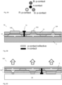
- Figs 5C and 5D show examples of a microLED device 500 where the semiconductor device 50 is connected to a driver circuit.
- Fig. 5A shows a top view of one example of a triangular arrangement of RGB mircoLED structures, where an n-contact is centrally configured in the triangular pixel arrangement. Separate n-contacts to the respective microLED is another option.
- Fig. 5B schematically illustrates the semiconductor device 50 according to an example of the proposed solution.
- the semiconductor device 50 comprises an epiwafer 10, and a plurality of InGaN platelets 100, each InGaN platelet being monolithically grown on the epiwafer and having a top c-plane surface.
- An upper mask layer 200 having mask apertures 220 is provided over the InGaN platelets, wherein said mask apertures have a width which is smaller than said top c-plane surface.
- a plurality of microLED structures, comprising QW layers, is grown on the top c-plane surface in one of said mask apertures. In this example, one microLED is grown on each InGaN platelet. In the drawing, the growth layer 2 still remains, but this layer may be stripped or thinned before or after contacting.
- a contact spacer layer 51 may be applied over microLED structures, wherein p-contacts 52B, 52G, 52R to the respective InGaN platelet project through the contact spacer layer 51 and bond to the respective top c-plane surface of the microLED structures.
- the contact spacer layer 51 is a dielectric layer, which allows for the application of leads (not shown) to the p-contacts over the surface of the microLED device.
- An n-contact 53 for the group of pixels (or separate contacts) is formed to extend from a surface of the base side of the InGaN platelets to the top side of the semiconductor structure 50, for convenient connection of the driver circuit.
- the n-contact 53 may be a metal connection, according to the shown example.
- FIGs 5C and 5D schematically illustrate examples of a microLED device 500 based on the example of Fig. 5B , comprising the semiconductor device 50 according to the proposed solution.
- the drawing indicates attachment and connection of the semiconductor device 50 to a driver circuit 54.
- Each microLED structure has a top c-plane surface connectable to the driver circuit 54, by means of the respective connector 52R, 52G, 52B for generating light emission.
- the driver circuits 54 are here exemplified by Si CMOS driver circuits. In some examples, thin film active transistor drivers may instead or additionally be used. While the top image of Fig. 5A suggests triangular grouping of RGB pixels with a central n-contact, the lower images show a linear representation for the sake of simplicity. Either is possible.
- the p-contacts 52B, 52G, 52R, connected to the upper c-planes of the respective microLED structure may be reflective to increase light output.
- the base substrate 1 (see Fig. 1 ) is removed.
- the original growth layer 2 may, as mentioned, further be thinned or stripped.
- at least a portion of the growth layer 2 remains (potentially after thinning), acting as a lead for connecting the n-connector to the base side of the respective InGaN platelet.
- Fig. 5D shows an alternative to the example of Fig. 5C .
- the growth layer 2 is completely removed, as well as the growth mask 3.
- a Transparent connector layer 55 such as a Transparent Conducting Oxide (TCO), is deposited to the base surface of the semiconductor device 50, acting as a lead for connecting the n-connector to the base side of the respective InGaN platelet.
- TCO Transparent Conducting Oxide
- the epiwafer 10 of the microLED device 500 thus comprises the InGaN platelets and a transparent conducting layer which may comprises the mask layer 3 and a part of the growth layer 2 or a transparent oxide layer.
- Figs 6A and 6B schematically illustrate another example of the semiconductor device 60 according to the proposed solution, based on the embodiment exemplified with reference to Fig. 3B where more than one microLED structure is configured on a common InGaN platelet, whereas Figs 6C and 6D show examples of a microLED device 600 where the semiconductor device 60 is connected to a driver circuit.
- Fig. 6A shows a top view of one example of a triangular arrangement of RGB mircoLED structures, where an n-contact is centrally configured in the triangular pixel arrangement. Separate n-contacts to the respective microLED is another option.
- Fig. 6B schematically illustrates the semiconductor device 60 according to an example of the proposed solution, based on the embodiment exemplified with reference to Fig. 3B .
- the semiconductor device 60 comprises an epiwafer 10, and a plurality of InGaN platelets 100, each InGaN platelet being monolithically grown on the epiwafer and configured with a truncated pyramid shape with a top c-plane surface.
- An upper mask layer 200 having mask apertures 220 is provided over the InGaN platelets, wherein said mask apertures have a width which is smaller than said top c-plane surface.
- a plurality of microLED structures comprising QW layers, is grown on the top c-plane surface in one of said mask apertures.
- three apertures are configured in the upper mask layer over each InGaN platelet.
- the growth layer 2 still remains, but this layer may be stripped or thinned before or after contacting.
- a contact spacer layer 51 may be applied over microLED structures, wherein p-contacts 52B, 52G, 52R to the respective InGaN platelet project through the contact spacer layer 51 and bond to the respective top c-plane surface of the microLED structures.
- the contact spacer layer 51 is a dielectric layer, which allows for the application of leads (not shown) to the p-contacts over the surface of the microLED device.
- An n-contact 53 for the group of pixels (or separate contacts) is formed to extend from a surface of the base side of the InGaN platelets to the top side of the semiconductor structure 60, for convenient connection of the driver circuit.
- the n-contact 53 may be a metal connection, according to the shown example.
- FIGs 6C and 6D schematically illustrate examples of a microLED device 600 based on the example of Fig. 6B , comprising the semiconductor device 60 according to the proposed solution.
- the drawing indicates attachment and connection of the semiconductor device 60 to a driver circuit 54.
- Each microLED structure has a top c-plane surface connectable to the driver circuit 54, by means of the respective connector 52R, 52G, 52B for generating light emission.
- the driver circuits 54 are here exemplified by Si CMOS driver circuits. In some examples, thin film active transistor drivers may instead or additionally be used. While the top image of Fig. 6A suggests triangular grouping of RGB pixels with a central n-contact, the lower images show a linear representation for the sake of simplicity. Either is possible.
- the p-contacts 52B, 52G, 52R, connected to the upper c-planes of the respective microLED structure may be reflective to increase light output.
- the base substrate 1 (see Fig. 1 ) is removed.
- the original growth layer 2 may, as mentioned, further be thinned or stripped.
- At least a portion of the growth layer 2 remains (potentially after thinning), acting as a lead for connecting the n-connector to the base side of the respective InGaN platelet.
- Fig. 6D shows an alternative to the example of Fig. 6C .
- the growth layer 2 is completely removed, and also the growth mask 3 is removed in this example.
- a Transparent connector layer 55 such as a TCO, is deposited to the base surface of the semiconductor device 60, acting as a lead for connecting the n-connector to the base side of the respective InGaN platelet.
- the epiwafer 10 of the microLED device 600 thus comprises the InGaN platelets and a transparent conducting layer which may comprises the mask layer 3 and a part of the growth layer 2 or a transparent oxide layer.
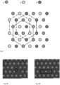
- Fig. 7 shows an example of microLED RGB array design according to some examples of the proposed solution.
- a hexagonal array is configured for each colour, as indicated in the drawing.
- the hexagonal pattern provides that the same distance/spacing is configured between all InGaN platelets prepared for the same emission wavelength. This is beneficial for growth uniformity. Specifically, by keeping trigonal symmetry (and centre-to-centre spacing) for red, green, and blue platelet LEDs, colour purity and uniformity across the wafer for each LED colour is very high. This arrangement is particularly suitable for use with the embodiment described with reference to Fig. 3A , where there is a one to one relationship between InGaN platelets and microLED structures.
- Fig. 8A shows one example of a pixel group configuration, where a triplet of RGB microLED structures is combined in one pixel group, capable of realizing any colour in the visible spectrum.
- a triangular pixel group is configured.
- Fig. 8B shows, by way of example, an alternative arrangement of a triplet of RGB microLED structures in one pixel group, capable of realizing any colour in the visible spectrum.
- a linear combination is configured.
- Fig. 9 shows an example of several pixel RGB groups, each comprising a triplet in accordance with the example of Fig. 8A .
- the pixel array layout demonstrates the arrangement of microLED structures for red, green, and blue light emission in a display application.
- the above-described embodiments provide examples of the proposed solution for a semiconductor device for microLEDs and a method of fabricating the same.
- the disclosed technology minimizes defects in crystal formation and improves external quantum efficiency for microLEDs with sub-10 ⁇ m pixel size. It further provides a solution for minimizing emission wavelength variation between microLED structures, epitaxially grown on the same wafer, intended to transmit light of the same wavelength.
- InGaN pyramids through mask openings 4 of the epiwafer 10 enables the formation of InGaN platelets 100 with a specific shape and configuration.
- This controlled growth process contributes to the overall quality and performance of the resulting microLEDs, as it allows for the formation of InGaN platelets with minimal defects and optimized external quantum efficiency.
- the growth mask 3, configured for growing InGaN pyramids, is preferably of a dielectric material such as AlO x , SiN x , TiN. Holes 4 opened through the dielectric growth mask are preferably placed in a trigonal lattice arrangement, as shown in Figs 9 -12, with hole dimensions in the 20-200 nm range and spaced 0.5 - 10 ⁇ m apart.
- the grown InGaN pyramids 5 are preferably grown as n-type InGaN.
- the n-type InGaN pyramids may be doped with e.g., Si to a level of 1-5 ⁇ 10 18 cm -3 .
- InGaN pyramids 5 of identical composition are concurrently grown, as n-type InGaN pyramids of certain indium concentration, wherein the pyramids are later processed to obtain separate InGaN platelets.
- GaN or InGaN pyramids with an indium content below 5% may be used.
- InGaN pyramids with an indium content around 10% (wavelength 420-430 nm) is preferred, and for red LEDs, 18%-20% indium contents (wavelength 480-500 nm) are preferred.
- Different content/concentration of indium may be obtained by growing the InGaN pyramids in separate processes.
- the microLED structures comprise a QW layer, also referred to as active layer, which as such may comprise one or more QWs, such as 3-5 QWs.
- Each QW of the QW layer may be about 2-3 nm thick.
- the compositions (i.e., the Indium concentration) for blue, green and red are about 10-15%, 25-27% and 35-40%, respectively.
- an electron blocking layer (EBL) of AlGaN with an Al content of 10-25% and a thickness of 10-25 nm may be used.
- an EBL of AlGaN Al content below 10%
- GaN or InGaN In content lower than n- and p-type InGaN layers
- a p-type InGaN top layer is further grown over the QW layer of the microLED structures.
- the p-layer may be p-GaN, or p-InGaN with only a few percent ( ⁇ 10% or ⁇ 5%) In, with a thickness of 100-200 nm.
- p-InGaN with an indium content of 10% and 18%, respectively may be used.
- the p-type doping is accomplished using e.g., Mg at a level at least above 1 ⁇ 10 19 cm -3 . Rapid thermal annealing may be used to activate the Mg doping.
- the contact spacer layer 51 can be a polymer.
- a dielectric spacer layer such as PECVD SiOx
- CMP to expose the top c-plane of p-InGaN layer.
- a thin layer of ALD Al 2 O 3 may be deposited first to protect the surface from being damaged by plasma at the beginning of SiOx deposition by PECVD and also to serve as surface passivation of the platelet surfaces.
- the n-type contacts to the base end of the InGaN platelets and the contacts to the p-type InGaN may be processed on the platelet side of the epiwafer 10, as shown in Figs 8B and 9B, which allows for convenient bonding to the driver circuits, such as CMOS driver chips.
- the flat c-plane top surface of the microLED structures provides a suitable surface for bonding of the p-contacts.
- the fabrication method for the semiconductor device for microLEDs described herein provides a robust and efficient approach to creating high-quality microLEDs with minimized defects in crystal formation and improved external quantum efficiency.
- the various steps and optional features of the method contribute to the formation of microLED structures with precise control over their shape, configuration, and emission properties, ensuring optimal performance of the resulting microLEDs in a wide range of applications.
- the proposed solution offers a huge advantage over prior art solutions.
- one color LED either blue, green or red
- mass transfer needs to be used to transfer sub-pixels of R, G, B microLEDs. This is a very challenging step, specifically not practical for the microLED below 10 ⁇ m.
- the proposed solution provides RGB sub-pixels on the same wafer in one growth step. This way, each full RGB pixel, containing three R/G/B sub-pixels, can be directly bonded to the driving circuit, avoiding the usage of mass transfer.
- This provides monolithic integration of RGB platelet microLEDs by epitaxy, such as Metal-Organic Chemical Vapor Deposition (MOCVD).
- MOCVD Metal-Organic Chemical Vapor Deposition
- the proposed solution may be configured in accordance with any of the items set out below.
- each microLED structure further comprises a top InGaN layer (243) grown on the respective QW layer.
- Item 3 The semiconductor device of item 1 or 2, wherein a single mask aperture is configured over each InGaN platelet, wherein a single microLED is configured on each InGaN platelet.
- Item 4 The semiconductor device of any preceding item, wherein a plurality of mask apertures (221, 222, 223) is configured over each InGaN platelet, wherein a plurality of microLED structures (230, 240, 250) is configured on each InGaN platelet.
- Item 5 The semiconductor device of item 4, wherein three mask apertures are configured over each InGaN platelet, wherein respective microLED structures for red, green and blue emission are configured on each InGaN platelet.
- Item 6 The semiconductor device of any preceding item, wherein the aperture width correlates with emission wavelength from the respective microLED structure.
- Item 7 The semiconductor device of any preceding item, wherein the apertures are configured with increasing width for different emission wavelength of the respective microLED structure, in the order red-green-blue.
- each microLED structure comprises an InGaN surface layer (241) grown in the mask aperture over the top c-plane, wherein the QW layer is grown on the InGaN surface layer.
- Item 9 The semiconductor device of item 8, wherein the InGaN surface layer has decreasing indium concentration with increasing width of the aperture.
- Item 10 The semiconductor device of any preceding item, wherein the epiwafer comprises a lower mask layer with mask openings in which the grown InGaN platelets are configured.
- Item 11 The semiconductor device of any preceding item, wherein the top c-plane surface has a hexagonal footprint.
- Item 12 The semiconductor device of any preceding item, wherein the mask aperture has a substantially circular footprint.
- each microLED structure have a truncated pyramid shape terminating in a c-plane connector surface.
- Item 15 The microLED device of item 14, wherein the driver circuit is connected by separate p-contacts to a plurality of microLED structures configured on the same InGaN platelet.
- Item 16 A method of fabricating a semiconductor structure, comprising:
- Item 17 The method of item 16, further comprising: growing, on the respective QW layer, a top InGaN layer of the respective microLED structure.
- Item 18 The method of item 16 or 17, wherein forming InGaN platelets comprises:
- Item 19 The method of any of items 16-18, wherein forming mask apertures comprises forming the apertures with different width, wherein growing of the QW layers configures the microLED structures with different emission wavelength.
- Item 20 The method of any of items 16-19, further comprising: growing an InGaN surface layer in the mask aperture over the top c-plane, wherein the QW layer is grown on the InGaN surface layer.
- Item 21 The method of item 20, wherein the InGaN surface layer has decreasing indium concentration with increasing width of the aperture.
- Item 22 The method of any of items 16-21, wherein forming mask apertures comprises forming a single mask aperture over each InGaN platelet, wherein a single microLED structure is configured on each InGaN platelet.
- Item 23 The method of any of items 16-21, wherein forming mask apertures comprises forming a plurality of mask apertures over each InGaN platelet, wherein a plurality of microLED structures is configured on each InGaN platelet.
- Item 24 The method of any of items 16-21, wherein forming mask apertures comprises forming three mask apertures with different width over each InGaN platelet, wherein growing of the QW layers form three microLED structures with respectively red, green, and blue emission wavelength on each InGaN platelet.
- Item 25 The method of any of items 16 to 24, wherein the growing of QW layers on the InGaN platelets is performed in a common epitaxy process, for forming microLED structures for different emission wavelengths.
- Item 26 The method of any of items 16 to 25, wherein each microLED structure is grown to a truncated pyramid shape terminating in a c-plane connector surface.
Landscapes
- Led Devices (AREA)
Priority Applications (2)
| Application Number | Priority Date | Filing Date | Title |
|---|---|---|---|
| EP23213341.3A EP4564435B1 (de) | 2023-11-30 | 2023-11-30 | Halbleiterbauelement mit mikro-led-strukturen |
| PCT/EP2024/077613 WO2025113850A1 (en) | 2023-11-30 | 2024-10-01 | Semiconductor device comprising microled structures |
Applications Claiming Priority (1)
| Application Number | Priority Date | Filing Date | Title |
|---|---|---|---|
| EP23213341.3A EP4564435B1 (de) | 2023-11-30 | 2023-11-30 | Halbleiterbauelement mit mikro-led-strukturen |
Publications (3)
| Publication Number | Publication Date |
|---|---|
| EP4564435A1 true EP4564435A1 (de) | 2025-06-04 |
| EP4564435C0 EP4564435C0 (de) | 2026-01-28 |
| EP4564435B1 EP4564435B1 (de) | 2026-01-28 |
Family
ID=89029696
Family Applications (1)
| Application Number | Title | Priority Date | Filing Date |
|---|---|---|---|
| EP23213341.3A Active EP4564435B1 (de) | 2023-11-30 | 2023-11-30 | Halbleiterbauelement mit mikro-led-strukturen |
Country Status (2)
| Country | Link |
|---|---|
| EP (1) | EP4564435B1 (de) |
| WO (1) | WO2025113850A1 (de) |
Citations (2)
| Publication number | Priority date | Publication date | Assignee | Title |
|---|---|---|---|---|
| WO2020187986A1 (en) | 2019-03-18 | 2020-09-24 | Hexagem Ab | Semiconductor template and fabrication method |
| US20230155060A1 (en) * | 2020-03-27 | 2023-05-18 | Google Llc | Indium gallium nitride light emitting diodes with reduced strain |
-
2023
- 2023-11-30 EP EP23213341.3A patent/EP4564435B1/de active Active
-
2024
- 2024-10-01 WO PCT/EP2024/077613 patent/WO2025113850A1/en active Pending
Patent Citations (2)
| Publication number | Priority date | Publication date | Assignee | Title |
|---|---|---|---|---|
| WO2020187986A1 (en) | 2019-03-18 | 2020-09-24 | Hexagem Ab | Semiconductor template and fabrication method |
| US20230155060A1 (en) * | 2020-03-27 | 2023-05-18 | Google Llc | Indium gallium nitride light emitting diodes with reduced strain |
Also Published As
| Publication number | Publication date |
|---|---|
| EP4564435C0 (de) | 2026-01-28 |
| EP4564435B1 (de) | 2026-01-28 |
| WO2025113850A1 (en) | 2025-06-05 |
Similar Documents
| Publication | Publication Date | Title |
|---|---|---|
| US12588317B2 (en) | LED display device, method of controlling the same, and method of manufacturing an LED display device | |
| US11637093B2 (en) | Micro light-emitting diode display fabrication and assembly | |
| KR20180133436A (ko) | 상이한 색상의 led를 포함하는 일체형 다색 직시형 디스플레이와 이의 제조 방법 | |
| US11901493B2 (en) | Semiconductor devices incorporating quantum dots | |
| JP7787232B2 (ja) | Ledアレイ | |
| CN109148652A (zh) | 无机发光二极管显示面板及其制作方法和显示装置 | |
| KR20230013072A (ko) | 직시형 디스플레이용 서브픽셀 발광 다이오드 및 이의 제조 방법 | |
| TWI912314B (zh) | 顯示器、發光二極體結構及用於形成其之相關聯的方法 | |
| US20260020403A1 (en) | Monolithic rgb microled array | |
| EP4564435B1 (de) | Halbleiterbauelement mit mikro-led-strukturen | |
| CN112289899B (zh) | Micro LED晶圆结构及其制备方法 | |
| US20240243232A1 (en) | Micro-led dbr fabrication by electrochemical etching | |
| WO2024155513A1 (en) | Color filtering distributed bragg reflector for micro-light emitting diodes and method of fabricating the same | |
| EP4525045A1 (de) | Halbleiterstrukturen für mikro-leds | |
| EP4627628A1 (de) | Anzeige mit seitlichen mehrfarben-leuchtbauelementpixeln und herstellungsverfahren dafür | |
| EP4609439A1 (de) | Mehrfarbige lichtemittierende mikro-led-anzeige und herstellungsverfahren dafür | |
| US20250185419A1 (en) | Nitride semiconductor light emitting device and display device having the same | |
| CN113451449A (zh) | 一种rgb外延结构及其制造方法与应用 | |
| CN119451331B (zh) | 一种GaN基微型LED显示单元及其制备方法 | |
| US20240243226A1 (en) | Resonant cavity micro-led fabrication | |
| US20240243225A1 (en) | Color filtering dbr for micro-leds | |
| CN115440858B (zh) | 一种用于全彩显示的RGB混合集成Micro-LED芯片阵列的制备方法 | |
| JP2025008930A (ja) | マイクロledの製造方法と発光素子および表示装置 | |
| WO2024155494A1 (en) | Micro-led dbr fabrication by electrochemical etching | |
| EP4652634A1 (de) | Herstellung von mikro-leds mit resonanzhohlraum |
Legal Events
| Date | Code | Title | Description |
|---|---|---|---|
| PUAI | Public reference made under article 153(3) epc to a published international application that has entered the european phase |
Free format text: ORIGINAL CODE: 0009012 |
|
| STAA | Information on the status of an ep patent application or granted ep patent |
Free format text: STATUS: REQUEST FOR EXAMINATION WAS MADE |
|
| 17P | Request for examination filed |
Effective date: 20240620 |
|
| AK | Designated contracting states |
Kind code of ref document: A1 Designated state(s): AL AT BE BG CH CY CZ DE DK EE ES FI FR GB GR HR HU IE IS IT LI LT LU LV MC ME MK MT NL NO PL PT RO RS SE SI SK SM TR |
|
| REG | Reference to a national code |
Ref legal event code: R079 Free format text: PREVIOUS MAIN CLASS: H01L0027150000 Ipc: H10H0029140000 Ref country code: DE Ref legal event code: R079 Ref document number: 602023011262 Country of ref document: DE Free format text: PREVIOUS MAIN CLASS: H01L0027150000 Ipc: H10H0029140000 |
|
| GRAP | Despatch of communication of intention to grant a patent |
Free format text: ORIGINAL CODE: EPIDOSNIGR1 |
|
| STAA | Information on the status of an ep patent application or granted ep patent |
Free format text: STATUS: GRANT OF PATENT IS INTENDED |
|
| RIC1 | Information provided on ipc code assigned before grant |
Ipc: H10H 29/14 20250101AFI20250918BHEP Ipc: H10H 20/01 20250101ALI20250918BHEP Ipc: H10H 20/815 20250101ALI20250918BHEP Ipc: H10H 20/817 20250101ALI20250918BHEP |
|
| INTG | Intention to grant announced |
Effective date: 20250930 |
|
| GRAS | Grant fee paid |
Free format text: ORIGINAL CODE: EPIDOSNIGR3 |
|
| GRAA | (expected) grant |
Free format text: ORIGINAL CODE: 0009210 |
|
| STAA | Information on the status of an ep patent application or granted ep patent |
Free format text: STATUS: THE PATENT HAS BEEN GRANTED |
|
| AK | Designated contracting states |
Kind code of ref document: B1 Designated state(s): AL AT BE BG CH CY CZ DE DK EE ES FI FR GB GR HR HU IE IS IT LI LT LU LV MC ME MK MT NL NO PL PT RO RS SE SI SK SM TR |
|
| REG | Reference to a national code |
Ref country code: CH Ref legal event code: F10 Free format text: ST27 STATUS EVENT CODE: U-0-0-F10-F00 (AS PROVIDED BY THE NATIONAL OFFICE) Effective date: 20260128 Ref country code: GB Ref legal event code: FG4D |
|
| REG | Reference to a national code |
Ref country code: CH Ref legal event code: W10 Free format text: ST27 STATUS EVENT CODE: U-0-0-W10-W00 (AS PROVIDED BY THE NATIONAL OFFICE) Effective date: 20260211 |
|
| REG | Reference to a national code |
Ref country code: IE Ref legal event code: FG4D |
|
| RAP4 | Party data changed (patent owner data changed or rights of a patent transferred) |
Owner name: HEXAGEM AB |
|
| U01 | Request for unitary effect filed |
Effective date: 20260202 |
|
| U07 | Unitary effect registered |
Designated state(s): AT BE BG DE DK EE FI FR IT LT LU LV MT NL PT RO SE SI Effective date: 20260206 |