EP4564409A1 - Bestückungsvorrichtung - Google Patents
Bestückungsvorrichtung Download PDFInfo
- Publication number
- EP4564409A1 EP4564409A1 EP23213527.7A EP23213527A EP4564409A1 EP 4564409 A1 EP4564409 A1 EP 4564409A1 EP 23213527 A EP23213527 A EP 23213527A EP 4564409 A1 EP4564409 A1 EP 4564409A1
- Authority
- EP
- European Patent Office
- Prior art keywords
- droplet
- electronic component
- pickup tool
- pick
- liquid
- Prior art date
- Legal status (The legal status is an assumption and is not a legal conclusion. Google has not performed a legal analysis and makes no representation as to the accuracy of the status listed.)
- Pending
Links
Images



Classifications
-
- H—ELECTRICITY
- H10—SEMICONDUCTOR DEVICES; ELECTRIC SOLID-STATE DEVICES NOT OTHERWISE PROVIDED FOR
- H10P—GENERIC PROCESSES OR APPARATUS FOR THE MANUFACTURE OR TREATMENT OF DEVICES COVERED BY CLASS H10
- H10P72/00—Handling or holding of wafers, substrates or devices during manufacture or treatment thereof
- H10P72/04—Apparatus for manufacture or treatment
- H10P72/0446—Apparatus for mounting on conductive members, e.g. leadframes or conductors on insulating substrates
Definitions
- aspects of the present disclosure relate to a pick-and-place apparatus and method for transferring an electronic component from a donor substrate towards an acceptor substrate. Aspects of the present disclosure particularly relate to pick-and-place apparatuses and methods for transferring electronic components such as semiconductor dies, either from a diced wafer or from a structured wafer, or packaged devices comprising one or more semiconductor dies.
- Pick-and-place apparatuses and methods for transferring an electronic component from a donor substrate towards an acceptor substrate are known in the art.
- An example of a known apparatus comprises a movable transfer module that includes at least one pickup tool, wherein each pickup tool is configured for picking up an electronic component.
- the pickup tool uses vacuum to capture and hold an electronic component that has been released from the donor substrate.
- the apparatus further comprises a drive unit that is mechanically coupled to the movable transfer module and that is configured for moving the transfer module.
- the pickup tool comprises a tool body with a narrow channel through which vacuum can be applied for attracting and holding an electronic component.
- the positioning of the electronic component on the pickup tool during transfer is fixed as the electronic component is firmly pulled against the tool body.
- the position and orientation of the electronic components relative to the pickup tool is subject to variation. Consequently, when the electronic component is released from the pickup tool and is transferred to the acceptor substrate, the position and orientation of the electronic component on the acceptor substrate may vary.
- the abovementioned variation in position and orientation of the electronic component on the acceptor substrate can be partially addressed by inspecting the position of the electronic component relative to the pickup tool using an optical camera and to move the acceptor substrate prior to receiving the electronic component to partially compensate for a positional offset of the electronic component relative to the pickup tool.
- the movement of the acceptor substate is performed in dependence of the readout by the optical camera.
- pick-and-place apparatuses of the type describe above present several disadvantages. Firstly, the throughput of the pick-and-place apparatuses can be hampered by the relatively slow switching speeds for switching the vacuum. Secondly, use of vacuum is less suitable for transferring small electronic components. Thirdly, as most acceptor stages used for holding and moving the acceptor substrates only allow a translational movement of the acceptor substrate, it is impossible or difficult to correct rotational offsets of the electronic component relative to the pickup tool.
- a pick-and-place apparatus that addresses at least one of the abovementioned drawbacks.
- this object is achieved by a pick-and-place apparatus that comprises a movable transfer module.
- This module comprises at least one pickup tool, wherein each pickup tool is configured for picking up an electronic component and comprises a tool body having a first surface.
- the apparatus further comprises a drive unit that is mechanically coupled to the movable transfer module and that is configured for moving the transfer module.
- the apparatus also includes a liquid droplet unit to provide, for each pickup tool, at least one droplet of a liquid on the first surface of that pickup tool for allowing an electronic component released from the donor substrate to be captured and held by said at least one droplet of liquid on said first surface.
- a liquid instead of a vacuum is used for holding the electronic component.
- the Applicant has found that by using a liquid, smaller devices can be efficiently transferred. Furthermore, delays associated with switching the vacuum on or off can be avoided, thereby improving the throughput of the apparatus.
- the apparatus may further comprise a first release unit for releasing an electronic component from the donor substrate, and a controller for controlling the liquid droplet unit, the drive unit, and the first release unit.
- the first release unit may comprise a light source, such as a laser.
- the donor substrate may comprise a film frame carrier in which a foil or film is clamped on which a structured or diced semiconductor wafer is arranged.
- the semiconductor dies can be attached to the film or foil using a light-sensitive or heat-sensitive adhesive that loses its adhesive properties when illuminated using light of suitable intensity and/or wavelength.
- the first release unit may comprise a mechanical release unit, such as a movable needle, that is configured to engage the electronic component to thereby release it from the donor substrate.
- the first release unit may comprise a needle that can be driven by an actuator, such as a pneumatic cylinder. The needle can be used to engage and push an electronic component away from the donor substrate.
- the controller can be configured to control the liquid droplet unit to provide at least one droplet of a liquid on the first surface of a given pickup tool among said at least one pickup tool, to control the drive unit to bring said given pickup tool into alignment with an electronic component to be released on the donor substrate, and to control the first release unit for releasing said electronic component.
- a typical order of events is that the at least one droplet of liquid is provided onto the first surface before the pickup tool is brought into alignment with an electronic component to be released.
- aligning the pickup tool with the electronic component to be released comprises bringing the pickup tool and donor substate into close proximity of one another leaving little space for providing the at least one droplet of liquid onto the first surface.
- the controller can be configured to control the drive unit to bring said given pickup tool into alignment with an empty placement position on the acceptor substrate thereby allowing the electronic component, which is held on the first surface of said given pickup tool by the at least one droplet of liquid, to be transferred from said pickup tool to the empty placement position on the acceptor substrate.
- the drive unit can be configured to rotate the transfer module about a rotational axis.
- the at least one pickup tool can each be configured to pick up an electronic component from a direction that is perpendicular to said rotational axis.
- the movable transfer module may have a cylindrical body of which an axial axis coincides with said rotational axis, and wherein each pickup tool is mounted to the cylindrical body.
- the at least one pickup took may comprise a plurality of pickup tools distributed at different angular positions on or in the cylindrical body, preferably with the same axial position.
- Each pickup tool may comprise a plurality of electrodes disposed in or on its tool body at or near its first surface.
- the pick-and-place apparatus may further comprise a supply unit for applying a potential difference over at least one pair of electrodes among the plurality of electrodes for the purpose of shaping and/or moving the at least one droplet of liquid on said first surface.
- a potential difference By applying a potential difference, an electric field can be generated at the first surface and inside the at least one droplet. This electric field can be used to shape, move, and/or orient the at least one droplet based on electrowetting and to thereby change the position and/or orientation of the electronic component relative to the pickup tool.
- the tool body may comprise a first body part and a second non-conductive hydrophobic body part.
- the second non-conductive hydrophobic body part is connected on a first side thereof to the first body part, while a second side thereof forms the first surface.
- the plurality of electrodes can be arranged on the first body part close to the first surface or in between the first body part and second non-conductive hydrophobic body part.
- the second non-conductive body part prevents electrical connection between the electrodes through the at least one droplet.
- the present disclosure is not limited thereto and embodiments are possible in which the electrodes come into direct contact with the at least one droplet.
- the at least one droplet may comprise a plurality of droplets.
- the plurality of electrodes may comprise a plurality of electrodes for each droplet among the plurality of droplets.
- the shape, position, and/or orientation of each droplet can preferably be changed independent from the other droplets by appropriately driving the electrodes that are associated with that droplet.
- the pick-and-place apparatus may further comprise an inspection unit, such as an optical camera, for determining an orientation and/or position of an electronic component held by the at least one droplet on the first surface of a given pickup tool among the at least one pickup tool.
- the apparatus may further comprise an alignment controller for controlling the supply unit in dependence of the determined orientation and/or position to adjust the orientation and/or position of the electronic component held by the at least one droplet of liquid by preferably individually shaping, moving, and/or orienting each droplet.
- This alignment controller is preferably part of or connected to the abovementioned controller.
- the liquid droplet unit may comprise a jetting or dripping unit to provide the at least droplet of liquid onto the first surface of a given pickup tool by means of jetting or dripping.
- the tool body of each pickup tool may comprise at least one channel exiting on the first surface for the formation of the at least one droplet, respectively, each channel being in fluid communication with a reservoir of said liquid.
- the pick-and-place apparatus may then further comprise, for each pickup tool, a pressure unit, such as a pump, for pumping the liquid through said at least one channel for forming the at least one droplet.
- the pick-and-place apparatus may also comprise a second release unit for at least partially removing the at least one droplet for the purpose of releasing the electronic component held by the at least one droplet, wherein the second release unit preferably comprises a light source, such as a laser.
- the second release unit may comprise one or more heaters for heating the electrodes such that the at least droplet at least partially evaporates.
- the one or more heaters can be provided on the pickup tool although the present disclosure is not limited thereto.
- the acceptor substrate and the movable transfer module or the pickup tool and acceptor substrate can be configured to a) move toward each other for the purpose of bringing the electronic component into contact with an adhesive layer on the acceptor substrate causing the adhesive layer to exert a force onto the electronic component that exceeds a force exerted on the electronic component by the at least one droplet, and b) move away from each other for allowing the electronic component to detach from the at least one drop and causing the electronic component to be held by the adhesive layer on the acceptor substrate.
- the acceptor substrate may be provided with an adhesive layer or spot at the placement position.
- the adhesive layer or spot may comprise a glue or solder.
- the adhesive layer or spot may exert a force onto the electronic component that exceeds the force by which the at least one droplet holds the electronic component.
- the pickup tool can be moved away from the acceptor substrate.
- the at least one droplet may remain attached to the electronic component after retracting the tool.
- the acceptor substrate is typically held at elevated temperatures to achieve sufficient adhesiveness of the adhesive layer. The elevated temperatures may therefore cause the at least one droplet to evaporate.
- the relative movement of the pickup tool and acceptor substrate required for the abovementioned release of the electronic component can be realized by moving the movable transfer module in a first direction whereas the acceptor substrate is not moved in this direction, by moving the acceptor substrate in a direction opposite to the first direction whereas the movable transfer module is not moved in this direction, or by moving both the acceptor substrate and movable transfer module.
- moving the movable transfer module in its entirety it may also be possible to move the pickup tool relative to a remainder of the movable transfer module.
- the at least one droplet of a liquid may comprise a droplet of water, de-ionized water, alcohol or glycerol.
- a method for transferring an electronic component comprises providing a pickup tool that comprises a tool body having a first surface on which at least one droplet of a liquid is arranged, releasing an electronic component from a donor substrate, capturing and holding the released electronic component using the at least one drop of liquid on the first surface, bringing the pickup tool into alignment with an empty placement position on an acceptor substrate, and transferring the electronic component from the pickup tool to the empty placement position.
- the method may additionally comprise changing the position and/or orientation of the electronic component by changing the shape, position, and/or orientation of the at least one droplet using electrowetting, prior to transferring the electronic component.
- a pick-and-place apparatus 100 is shown in accordance with the present disclosure. It comprises a movable transfer module in the form of a turret 110.
- turret 110 is provided with four pickup tools 120, of which examples are shown in figure 3 .
- turret 110 can be rotated about an axis A1.
- Figure 1 further illustrates a donor substrate 130 provided in the form of a film frame carrier on which a diced semiconductor is arranged. More in particular, donor substrate 130 comprises a film 131 on which an adhesive layer 132 is provided by which semiconductor dies 133 of a diced semiconductor wafer are arranged. Although explained using semiconductor dies 133, apparatus 100 can be configured for transferring other electronic components such as LEDs and passives.
- Donor substrate 130 is supported by a donor stage (not shown).
- a donor stage driver may be used to control the donor stage for moving donor substrate 130.
- the donor stage is able to move donor substrate 130 in the x-y plane.
- Figure 1 further illustrates an acceptor substrate 140 that is supported by an acceptor stage (not shown).
- An acceptor stage driver may be used to control the acceptor stage for moving acceptor substrate 140.
- the acceptor stage is able to move acceptor substrate 140 in the x-y plane.
- a plurality of placement positions A is defined on acceptor substrate 140. At these positions, an adhesive 141 is provided.
- Apparatus 100 comprises a liquid droplet unit 160 to provide a droplet 161 of liquid onto pickup tool 120.
- liquid droplet unit 160 can be configured to provide droplet 161 by means of jetting or dripping.
- Apparatus 100 also comprises a first release unit 150 that comprises a laser source that emits a beam 151 that is focused by a lens 152 onto a donor position P at which a semiconductor die 133 is attached to film 131.
- adhesive layer 132 which is typically heat-sensitive or light-sensitive, loses its adhesive properties causing semiconductor die 133 to become detached from film 131.
- semiconductor die 133 will fall downward onto a droplet 161 on a pickup tool 120 that was previously aligned with donor position P. Additionally, or alternatively, absorption of light by adhesive layer 132 may cause this layer to at least partially ablate thereby causing a propelling force that pushes semiconductor die 133 toward pickup tool 120.
- apparatus 100 may comprise a mechanical release unit for releasing semiconductor dies 133 from film 131.
- a movable needle can be used that punches through film 131 on which semiconductor dies 133 are placed.
- Such needle can be driven using a pneumatic cylinder or the like.
- turret 110 is rotated to bring pickup tool 120 into a position in which an image of semiconductor die 133 can be obtained using inspection system 170 that comprises an optical camera. Inspection system 170 determines the position and/or orientation of semiconductor die 133 relative to pickup tool 120.
- turret 110 is rotated further to bring pickup tool 120 into alignment with a placement position A on acceptor substrate 140.
- acceptor substrate 140 may have been moved to bring an empty position into alignment with pickup 120.
- acceptor substrate 140 may have been moved to account for a positional offset that was determined using inspection system 170.
- a correction can additionally or alternatively be performed differently as will be explained later.
- pickup tool 120 After aligning pickup tool 120 and acceptor substrate 140, semiconductor die 133 can be released. As shown in figure 1 , pickup tool 120 is moved toward acceptor substrate 140 in such a manner that semiconductor die 133 touches adhesive 141. More in particular, pickup tool 120 is moved such that the force exerted on semiconductor die 133 by adhesive exceeds the force exerted by droplet 161 on semiconductor die 133.
- Movement of pickup tool 120 can be realized by moving turret 110 in its entirety.
- pickup tool 120 can be moved relative to a remainder of turret 110.
- pickup tool 120 can be connected to a hydraulic cylinder.
- movement of pickup tool 120 is replaced by or complemented with a movement of acceptor substrate 140 toward turret 110.
- pickup tool 120 can moved back. During this motion, semiconductor die 133 will remain attached to acceptor substrate 140 through adhesive 141 as the latter exerts a stronger force on semiconductor die 133 than droplet 161.
- droplet 161, or what still remains of droplet 161 on pickup tool 120 after having released semiconductor die 133, may be removed prior to arranging a new droplet 161 by liquid droplet unit 160, for example by means of heating.
- Apparatus 100 is schematically illustrated in figure 2 .
- Apparatus 100 comprises a controller 180 that receives information from inspection system 170. Controller 180 controls liquid droplet unit 160, first release unit 150, an acceptor stage driver 149 that moves an acceptor stage that holds acceptor substrate 140, a donor stage driver 139 that moves a donor stage that holds donor substrate 130, a turret driver 111 for rotating turret 110, and a second release unit 190.
- This latter release unit may comprise a driver for mutually moving acceptor substrate 140 and pickup tool 120.
- This driver may comprise a pneumatic cylinder connected to pickup tool 120 and/or the driver may be configured for moving acceptor substrate 140 and/or turret 110.
- second release unit 190 may comprise heating means for heating droplet 161 for the purpose of causing semiconductor die 133 to be released from pickup tool 120 and/or for the purpose of removing what still remains of droplet 161 on pickup tool 120 after having released semiconductor die 133.
- These heating means may comprise a light source.
- Apparatus 100 may further comprise an alignment controller 195 that controls a supply unit 196 and that is controlled by controller 170 to change the position and/or orientation of semiconductor die 133 relative to pickup tool 120. This will be explained referring to figure 3 .
- FIG. 3 illustrates a pickup tool 120A.
- a top view is shown, as well as a cross-sectional view taken along line 129A.
- Pickup tool 120A comprises a non-conductive hydrophobic part 121A and a second part 122A, which parts are both comprised by pickup tool body 126A.
- a side of part 121A defines a first surface 125A of pickup tool 120A.
- a plurality of electrodes 123A is arranged in between parts 121A and 122A.
- Circles 124A indicate intended positions for a droplet 161 of liquid.
- pickup tool 120A is configured to hold semiconductor die 133 using four droplets 161.
- first surface 125A By applying a potential difference over electrodes 123A, the wetting properties of first surface 125A can be modified. This will cause droplets 161 arranged at circles 124A to change shape, orientation, and/or position. Consequently, the position and/orientation of a semiconductor die 133 attached to pickup tool 120A using droplets 161 can be changed accordingly.
- figure 3 illustrates a pickup tool 120B.
- a top view is shown, as well as a cross-sectional view taken along line 129B.
- pickup tool 120B comprises a non-conductive hydrophobic part 121B and a second part 122B.
- a side of part 121A defines a first surface 125B of pickup tool 120B.
- a plurality of electrodes 123B is arranged in between parts 121B and 122B.
- Circle 124B indicates an intended position for a single droplet 161 of liquid. Put differently, unlike pickup tool 120A, pickup tool 120B is configured to hold semiconductor die 133 using a single droplet 161.
- Pickup tool 120B further defines a channel 127B through which liquid can be transported for forming a droplet 161 on first surface 125B.
- channel 127B can be in fluid communication with a reservoir (not shown) of the liquid.
- a pump may be used for pumping fluid from the reservoir through channel 127B.
- Such a pump may be provided for each pickup tool 120B separately.
- the liquid droplet unit is not external from turret 110 as shown in figure 1 but may comprise the pump(s) required for pumping the liquid though channels 127B of pickup tools 120B. These pumps may be controlled using controller 180.
- a pickup tool may have one or more channels for arranging one or more droplets on the first surface of which the shape, position, and/or orientation are controlled using one or more electrodes.
- sets of electrodes can be defined for each droplet for individually controlling the shape, position, and/or orientation of the droplets.
- Pickup tool 120A for example has a set of four electrodes 123A for each droplet 161.
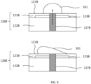
- Figure 4 illustrates an example of changing droplet 161 using electrodes 123B for pickup tool 123B.
- the top figure illustrates the situation after transporting liquid through channel 127B for forming droplet 161 without applying a potential difference over the pair of electrodes 123B.
- a potential difference has been applied over the pair of electrodes 123B causing a deformation of droplet 161 as a result of electrowetting.
- Electrodes 123A, 123B can be controlled using supply unit 195 shown in figure 2 .
- supply unit 196 may control the potential of each electrode 123A, 123B relative to a reference potential.
- the potential of one or more electrodes 123A, 123B may be set to this reference potential.
- supply unit 196 is controlled by alignment controller 195 in dependence of the information from inspection system 170.
- Figure 5 illustrates a method for transferring an electronic component in accordance with the present disclosure.
- This method comprises a step S1 of providing a pickup tool that comprises a tool body having a first surface on which at least one droplet of a liquid is arranged, and a step S2 of releasing an electronic component from a donor substrate.
- the method further comprises a step S3 of capturing and holding the released electronic component using the at least one drop of liquid on the first surface, and a step S4 of bringing the pickup tool into alignment with an empty placement position on an acceptor substrate.
- the method may comprise a step S5 of transferring the electronic component from the pickup tool to the empty placement position.
Landscapes
- Coating Apparatus (AREA)
Priority Applications (2)
| Application Number | Priority Date | Filing Date | Title |
|---|---|---|---|
| EP23213527.7A EP4564409A1 (de) | 2023-11-30 | 2023-11-30 | Bestückungsvorrichtung |
| PCT/EP2024/084153 WO2025114563A1 (en) | 2023-11-30 | 2024-11-29 | Pick-and-place apparatus |
Applications Claiming Priority (1)
| Application Number | Priority Date | Filing Date | Title |
|---|---|---|---|
| EP23213527.7A EP4564409A1 (de) | 2023-11-30 | 2023-11-30 | Bestückungsvorrichtung |
Publications (1)
| Publication Number | Publication Date |
|---|---|
| EP4564409A1 true EP4564409A1 (de) | 2025-06-04 |
Family
ID=89029964
Family Applications (1)
| Application Number | Title | Priority Date | Filing Date |
|---|---|---|---|
| EP23213527.7A Pending EP4564409A1 (de) | 2023-11-30 | 2023-11-30 | Bestückungsvorrichtung |
Country Status (2)
| Country | Link |
|---|---|
| EP (1) | EP4564409A1 (de) |
| WO (1) | WO2025114563A1 (de) |
Citations (4)
| Publication number | Priority date | Publication date | Assignee | Title |
|---|---|---|---|---|
| US20120292775A1 (en) * | 2009-12-28 | 2012-11-22 | Tokyo Electron Limited | Mounting method and mounting device |
| US20190252350A1 (en) * | 2016-10-28 | 2019-08-15 | Osram Opto Semiconductors Gmbh | Semiconductor chip transfer method and transfer tool |
| US20210339964A1 (en) * | 2018-08-23 | 2021-11-04 | Lg Display Co., Ltd. | Transportation head for microchip transfer device, microchip transfer device having same, and transfer method thereby |
| US20220277980A1 (en) * | 2019-11-08 | 2022-09-01 | Semiconductor Technologies & Instruments Pte Ltd | Component handler |
-
2023
- 2023-11-30 EP EP23213527.7A patent/EP4564409A1/de active Pending
-
2024
- 2024-11-29 WO PCT/EP2024/084153 patent/WO2025114563A1/en active Pending
Patent Citations (4)
| Publication number | Priority date | Publication date | Assignee | Title |
|---|---|---|---|---|
| US20120292775A1 (en) * | 2009-12-28 | 2012-11-22 | Tokyo Electron Limited | Mounting method and mounting device |
| US20190252350A1 (en) * | 2016-10-28 | 2019-08-15 | Osram Opto Semiconductors Gmbh | Semiconductor chip transfer method and transfer tool |
| US20210339964A1 (en) * | 2018-08-23 | 2021-11-04 | Lg Display Co., Ltd. | Transportation head for microchip transfer device, microchip transfer device having same, and transfer method thereby |
| US20220277980A1 (en) * | 2019-11-08 | 2022-09-01 | Semiconductor Technologies & Instruments Pte Ltd | Component handler |
Also Published As
| Publication number | Publication date |
|---|---|
| WO2025114563A1 (en) | 2025-06-05 |
Similar Documents
| Publication | Publication Date | Title |
|---|---|---|
| KR101606215B1 (ko) | 태양 전지 기판용 비접촉식 모서리 코팅 장치를 위한 제어 시스템 | |
| US10490525B1 (en) | High speed handling of ultra-small chips by selective laser bonding and debonding | |
| KR101600411B1 (ko) | 태양 전지 기판용 비접촉식 에지 코팅 장치 및 이를 이용하는 방법 | |
| US20200294976A1 (en) | Method for constructing micro-led display module | |
| JP6716391B2 (ja) | 実装方法および実装装置 | |
| KR20190116981A (ko) | 부품 실장 시스템, 수지 성형 장치, 수지 탑재 장치, 부품 실장 방법 및 수지 성형 방법 | |
| CN111243999B (zh) | 微元件的转移装置及转移方法 | |
| JP4372605B2 (ja) | 電子部品搭載装置および電子部品搭載方法 | |
| US11495571B2 (en) | Mounting method and mounting device | |
| JP6941513B2 (ja) | 半導体製造装置および半導体装置の製造方法 | |
| US20220302077A1 (en) | Bonding apparatus, bonding system, and bonding method | |
| JP6454812B1 (ja) | ワーク転写用チャック及びワーク転写方法 | |
| EP4564409A1 (de) | Bestückungsvorrichtung | |
| US6596115B1 (en) | Method and device for carrying out working steps on miniaturized modules | |
| JP2006147725A (ja) | チップ搭載機およびチップ搭載方法 | |
| US20230402308A1 (en) | Transfer device for transferring an electronic component | |
| KR102876238B1 (ko) | 다이 본더 | |
| JP4766258B2 (ja) | 板状物品のピックアップ装置 | |
| KR20240015581A (ko) | 웨이퍼 필름 프레임에서 칩을 제거하는 방법 및 장치,배치 시스템 및 컴퓨터 프로그램 | |
| US20240332448A1 (en) | Method for applying an electrical connection material or flux material to a component | |
| US11328942B1 (en) | Liquid crystalline elastomer for pick and place of semiconductor devices | |
| JP4221360B2 (ja) | キャリアによって支持されるコンポーネントの基板上の所望の位置への移動に好適な方法、及びこのために設計される装置 | |
| US20250167170A1 (en) | Laser transfer of microelectronic device and associated conductive pad | |
| KR102888166B1 (ko) | 반도체 제조 장치, 박리 유닛 및 반도체 장치의 제조 방법 | |
| JP2024106269A (ja) | 半導体製造装置、剥離ユニットおよび半導体装置の製造方法 |
Legal Events
| Date | Code | Title | Description |
|---|---|---|---|
| PUAI | Public reference made under article 153(3) epc to a published international application that has entered the european phase |
Free format text: ORIGINAL CODE: 0009012 |
|
| STAA | Information on the status of an ep patent application or granted ep patent |
Free format text: STATUS: THE APPLICATION HAS BEEN PUBLISHED |
|
| AK | Designated contracting states |
Kind code of ref document: A1 Designated state(s): AL AT BE BG CH CY CZ DE DK EE ES FI FR GB GR HR HU IE IS IT LI LT LU LV MC ME MK MT NL NO PL PT RO RS SE SI SK SM TR |
|
| STAA | Information on the status of an ep patent application or granted ep patent |
Free format text: STATUS: REQUEST FOR EXAMINATION WAS MADE |
|
| 17P | Request for examination filed |
Effective date: 20251204 |