EP4560663A2 - Mehrschichtiges elektronisches bauteil - Google Patents
Mehrschichtiges elektronisches bauteil Download PDFInfo
- Publication number
- EP4560663A2 EP4560663A2 EP24205770.1A EP24205770A EP4560663A2 EP 4560663 A2 EP4560663 A2 EP 4560663A2 EP 24205770 A EP24205770 A EP 24205770A EP 4560663 A2 EP4560663 A2 EP 4560663A2
- Authority
- EP
- European Patent Office
- Prior art keywords
- moles
- component
- sub
- multilayer electronic
- electronic component
- Prior art date
- Legal status (The legal status is an assumption and is not a legal conclusion. Google has not performed a legal analysis and makes no representation as to the accuracy of the status listed.)
- Pending
Links
Images

Classifications
-
- H—ELECTRICITY
- H01—ELECTRIC ELEMENTS
- H01G—CAPACITORS; CAPACITORS, RECTIFIERS, DETECTORS, SWITCHING DEVICES, LIGHT-SENSITIVE OR TEMPERATURE-SENSITIVE DEVICES OF THE ELECTROLYTIC TYPE
- H01G4/00—Fixed capacitors; Processes of their manufacture
- H01G4/002—Details
- H01G4/018—Dielectrics
- H01G4/06—Solid dielectrics
- H01G4/08—Inorganic dielectrics
- H01G4/12—Ceramic dielectrics
- H01G4/1209—Ceramic dielectrics characterised by the ceramic dielectric material
- H01G4/1236—Ceramic dielectrics characterised by the ceramic dielectric material based on zirconium oxides or zirconates
- H01G4/1245—Ceramic dielectrics characterised by the ceramic dielectric material based on zirconium oxides or zirconates containing also titanates
-
- H—ELECTRICITY
- H01—ELECTRIC ELEMENTS
- H01G—CAPACITORS; CAPACITORS, RECTIFIERS, DETECTORS, SWITCHING DEVICES, LIGHT-SENSITIVE OR TEMPERATURE-SENSITIVE DEVICES OF THE ELECTROLYTIC TYPE
- H01G4/00—Fixed capacitors; Processes of their manufacture
- H01G4/002—Details
- H01G4/018—Dielectrics
- H01G4/06—Solid dielectrics
- H01G4/08—Inorganic dielectrics
- H01G4/12—Ceramic dielectrics
- H01G4/1209—Ceramic dielectrics characterised by the ceramic dielectric material
- H01G4/1236—Ceramic dielectrics characterised by the ceramic dielectric material based on zirconium oxides or zirconates
-
- C—CHEMISTRY; METALLURGY
- C04—CEMENTS; CONCRETE; ARTIFICIAL STONE; CERAMICS; REFRACTORIES
- C04B—LIME, MAGNESIA; SLAG; CEMENTS; COMPOSITIONS THEREOF, e.g. MORTARS, CONCRETE OR LIKE BUILDING MATERIALS; ARTIFICIAL STONE; CERAMICS; REFRACTORIES; TREATMENT OF NATURAL STONE
- C04B35/00—Shaped ceramic products characterised by their composition; Ceramics compositions; Processing powders of inorganic compounds preparatory to the manufacturing of ceramic products
- C04B35/01—Shaped ceramic products characterised by their composition; Ceramics compositions; Processing powders of inorganic compounds preparatory to the manufacturing of ceramic products based on oxide ceramics
- C04B35/48—Shaped ceramic products characterised by their composition; Ceramics compositions; Processing powders of inorganic compounds preparatory to the manufacturing of ceramic products based on oxide ceramics based on zirconium or hafnium oxides, zirconates, zircon or hafnates
- C04B35/49—Shaped ceramic products characterised by their composition; Ceramics compositions; Processing powders of inorganic compounds preparatory to the manufacturing of ceramic products based on oxide ceramics based on zirconium or hafnium oxides, zirconates, zircon or hafnates containing also titanium oxides or titanates
-
- H—ELECTRICITY
- H01—ELECTRIC ELEMENTS
- H01G—CAPACITORS; CAPACITORS, RECTIFIERS, DETECTORS, SWITCHING DEVICES, LIGHT-SENSITIVE OR TEMPERATURE-SENSITIVE DEVICES OF THE ELECTROLYTIC TYPE
- H01G4/00—Fixed capacitors; Processes of their manufacture
- H01G4/002—Details
- H01G4/005—Electrodes
- H01G4/012—Form of non-self-supporting electrodes
-
- H—ELECTRICITY
- H01—ELECTRIC ELEMENTS
- H01G—CAPACITORS; CAPACITORS, RECTIFIERS, DETECTORS, SWITCHING DEVICES, LIGHT-SENSITIVE OR TEMPERATURE-SENSITIVE DEVICES OF THE ELECTROLYTIC TYPE
- H01G4/00—Fixed capacitors; Processes of their manufacture
- H01G4/002—Details
- H01G4/018—Dielectrics
- H01G4/06—Solid dielectrics
- H01G4/08—Inorganic dielectrics
- H01G4/12—Ceramic dielectrics
- H01G4/1209—Ceramic dielectrics characterised by the ceramic dielectric material
- H01G4/1218—Ceramic dielectrics characterised by the ceramic dielectric material based on titanium oxides or titanates
- H01G4/1227—Ceramic dielectrics characterised by the ceramic dielectric material based on titanium oxides or titanates based on alkaline earth titanates
-
- H—ELECTRICITY
- H01—ELECTRIC ELEMENTS
- H01G—CAPACITORS; CAPACITORS, RECTIFIERS, DETECTORS, SWITCHING DEVICES, LIGHT-SENSITIVE OR TEMPERATURE-SENSITIVE DEVICES OF THE ELECTROLYTIC TYPE
- H01G4/00—Fixed capacitors; Processes of their manufacture
- H01G4/002—Details
- H01G4/228—Terminals
- H01G4/232—Terminals electrically connecting two or more layers of a stacked or rolled capacitor
-
- H—ELECTRICITY
- H01—ELECTRIC ELEMENTS
- H01G—CAPACITORS; CAPACITORS, RECTIFIERS, DETECTORS, SWITCHING DEVICES, LIGHT-SENSITIVE OR TEMPERATURE-SENSITIVE DEVICES OF THE ELECTROLYTIC TYPE
- H01G4/00—Fixed capacitors; Processes of their manufacture
- H01G4/30—Stacked capacitors
-
- C—CHEMISTRY; METALLURGY
- C04—CEMENTS; CONCRETE; ARTIFICIAL STONE; CERAMICS; REFRACTORIES
- C04B—LIME, MAGNESIA; SLAG; CEMENTS; COMPOSITIONS THEREOF, e.g. MORTARS, CONCRETE OR LIKE BUILDING MATERIALS; ARTIFICIAL STONE; CERAMICS; REFRACTORIES; TREATMENT OF NATURAL STONE
- C04B2235/00—Aspects relating to ceramic starting mixtures or sintered ceramic products
- C04B2235/02—Composition of constituents of the starting material or of secondary phases of the final product
- C04B2235/30—Constituents and secondary phases not being of a fibrous nature
- C04B2235/32—Metal oxides, mixed metal oxides, or oxide-forming salts thereof, e.g. carbonates, nitrates, (oxy)hydroxides, chlorides
- C04B2235/3205—Alkaline earth oxides or oxide forming salts thereof, e.g. beryllium oxide
- C04B2235/3208—Calcium oxide or oxide-forming salts thereof, e.g. lime
-
- C—CHEMISTRY; METALLURGY
- C04—CEMENTS; CONCRETE; ARTIFICIAL STONE; CERAMICS; REFRACTORIES
- C04B—LIME, MAGNESIA; SLAG; CEMENTS; COMPOSITIONS THEREOF, e.g. MORTARS, CONCRETE OR LIKE BUILDING MATERIALS; ARTIFICIAL STONE; CERAMICS; REFRACTORIES; TREATMENT OF NATURAL STONE
- C04B2235/00—Aspects relating to ceramic starting mixtures or sintered ceramic products
- C04B2235/02—Composition of constituents of the starting material or of secondary phases of the final product
- C04B2235/30—Constituents and secondary phases not being of a fibrous nature
- C04B2235/32—Metal oxides, mixed metal oxides, or oxide-forming salts thereof, e.g. carbonates, nitrates, (oxy)hydroxides, chlorides
- C04B2235/3205—Alkaline earth oxides or oxide forming salts thereof, e.g. beryllium oxide
- C04B2235/3213—Strontium oxides or oxide-forming salts thereof
-
- C—CHEMISTRY; METALLURGY
- C04—CEMENTS; CONCRETE; ARTIFICIAL STONE; CERAMICS; REFRACTORIES
- C04B—LIME, MAGNESIA; SLAG; CEMENTS; COMPOSITIONS THEREOF, e.g. MORTARS, CONCRETE OR LIKE BUILDING MATERIALS; ARTIFICIAL STONE; CERAMICS; REFRACTORIES; TREATMENT OF NATURAL STONE
- C04B2235/00—Aspects relating to ceramic starting mixtures or sintered ceramic products
- C04B2235/02—Composition of constituents of the starting material or of secondary phases of the final product
- C04B2235/30—Constituents and secondary phases not being of a fibrous nature
- C04B2235/32—Metal oxides, mixed metal oxides, or oxide-forming salts thereof, e.g. carbonates, nitrates, (oxy)hydroxides, chlorides
- C04B2235/3224—Rare earth oxide or oxide forming salts thereof, e.g. scandium oxide
- C04B2235/3225—Yttrium oxide or oxide-forming salts thereof
-
- C—CHEMISTRY; METALLURGY
- C04—CEMENTS; CONCRETE; ARTIFICIAL STONE; CERAMICS; REFRACTORIES
- C04B—LIME, MAGNESIA; SLAG; CEMENTS; COMPOSITIONS THEREOF, e.g. MORTARS, CONCRETE OR LIKE BUILDING MATERIALS; ARTIFICIAL STONE; CERAMICS; REFRACTORIES; TREATMENT OF NATURAL STONE
- C04B2235/00—Aspects relating to ceramic starting mixtures or sintered ceramic products
- C04B2235/02—Composition of constituents of the starting material or of secondary phases of the final product
- C04B2235/30—Constituents and secondary phases not being of a fibrous nature
- C04B2235/32—Metal oxides, mixed metal oxides, or oxide-forming salts thereof, e.g. carbonates, nitrates, (oxy)hydroxides, chlorides
- C04B2235/3231—Refractory metal oxides, their mixed metal oxides, or oxide-forming salts thereof
- C04B2235/3239—Vanadium oxides, vanadates or oxide forming salts thereof, e.g. magnesium vanadate
-
- C—CHEMISTRY; METALLURGY
- C04—CEMENTS; CONCRETE; ARTIFICIAL STONE; CERAMICS; REFRACTORIES
- C04B—LIME, MAGNESIA; SLAG; CEMENTS; COMPOSITIONS THEREOF, e.g. MORTARS, CONCRETE OR LIKE BUILDING MATERIALS; ARTIFICIAL STONE; CERAMICS; REFRACTORIES; TREATMENT OF NATURAL STONE
- C04B2235/00—Aspects relating to ceramic starting mixtures or sintered ceramic products
- C04B2235/02—Composition of constituents of the starting material or of secondary phases of the final product
- C04B2235/30—Constituents and secondary phases not being of a fibrous nature
- C04B2235/32—Metal oxides, mixed metal oxides, or oxide-forming salts thereof, e.g. carbonates, nitrates, (oxy)hydroxides, chlorides
- C04B2235/3231—Refractory metal oxides, their mixed metal oxides, or oxide-forming salts thereof
- C04B2235/3241—Chromium oxides, chromates, or oxide-forming salts thereof
-
- C—CHEMISTRY; METALLURGY
- C04—CEMENTS; CONCRETE; ARTIFICIAL STONE; CERAMICS; REFRACTORIES
- C04B—LIME, MAGNESIA; SLAG; CEMENTS; COMPOSITIONS THEREOF, e.g. MORTARS, CONCRETE OR LIKE BUILDING MATERIALS; ARTIFICIAL STONE; CERAMICS; REFRACTORIES; TREATMENT OF NATURAL STONE
- C04B2235/00—Aspects relating to ceramic starting mixtures or sintered ceramic products
- C04B2235/02—Composition of constituents of the starting material or of secondary phases of the final product
- C04B2235/30—Constituents and secondary phases not being of a fibrous nature
- C04B2235/32—Metal oxides, mixed metal oxides, or oxide-forming salts thereof, e.g. carbonates, nitrates, (oxy)hydroxides, chlorides
- C04B2235/3262—Manganese oxides, manganates, rhenium oxides or oxide-forming salts thereof, e.g. MnO
-
- C—CHEMISTRY; METALLURGY
- C04—CEMENTS; CONCRETE; ARTIFICIAL STONE; CERAMICS; REFRACTORIES
- C04B—LIME, MAGNESIA; SLAG; CEMENTS; COMPOSITIONS THEREOF, e.g. MORTARS, CONCRETE OR LIKE BUILDING MATERIALS; ARTIFICIAL STONE; CERAMICS; REFRACTORIES; TREATMENT OF NATURAL STONE
- C04B2235/00—Aspects relating to ceramic starting mixtures or sintered ceramic products
- C04B2235/02—Composition of constituents of the starting material or of secondary phases of the final product
- C04B2235/30—Constituents and secondary phases not being of a fibrous nature
- C04B2235/32—Metal oxides, mixed metal oxides, or oxide-forming salts thereof, e.g. carbonates, nitrates, (oxy)hydroxides, chlorides
- C04B2235/327—Iron group oxides, their mixed metal oxides, or oxide-forming salts thereof
- C04B2235/3272—Iron oxides or oxide forming salts thereof, e.g. hematite, magnetite
-
- C—CHEMISTRY; METALLURGY
- C04—CEMENTS; CONCRETE; ARTIFICIAL STONE; CERAMICS; REFRACTORIES
- C04B—LIME, MAGNESIA; SLAG; CEMENTS; COMPOSITIONS THEREOF, e.g. MORTARS, CONCRETE OR LIKE BUILDING MATERIALS; ARTIFICIAL STONE; CERAMICS; REFRACTORIES; TREATMENT OF NATURAL STONE
- C04B2235/00—Aspects relating to ceramic starting mixtures or sintered ceramic products
- C04B2235/02—Composition of constituents of the starting material or of secondary phases of the final product
- C04B2235/30—Constituents and secondary phases not being of a fibrous nature
- C04B2235/32—Metal oxides, mixed metal oxides, or oxide-forming salts thereof, e.g. carbonates, nitrates, (oxy)hydroxides, chlorides
- C04B2235/327—Iron group oxides, their mixed metal oxides, or oxide-forming salts thereof
- C04B2235/3275—Cobalt oxides, cobaltates or cobaltites or oxide forming salts thereof, e.g. bismuth cobaltate, zinc cobaltite
-
- C—CHEMISTRY; METALLURGY
- C04—CEMENTS; CONCRETE; ARTIFICIAL STONE; CERAMICS; REFRACTORIES
- C04B—LIME, MAGNESIA; SLAG; CEMENTS; COMPOSITIONS THEREOF, e.g. MORTARS, CONCRETE OR LIKE BUILDING MATERIALS; ARTIFICIAL STONE; CERAMICS; REFRACTORIES; TREATMENT OF NATURAL STONE
- C04B2235/00—Aspects relating to ceramic starting mixtures or sintered ceramic products
- C04B2235/02—Composition of constituents of the starting material or of secondary phases of the final product
- C04B2235/30—Constituents and secondary phases not being of a fibrous nature
- C04B2235/32—Metal oxides, mixed metal oxides, or oxide-forming salts thereof, e.g. carbonates, nitrates, (oxy)hydroxides, chlorides
- C04B2235/327—Iron group oxides, their mixed metal oxides, or oxide-forming salts thereof
- C04B2235/3279—Nickel oxides, nickalates, or oxide-forming salts thereof
-
- C—CHEMISTRY; METALLURGY
- C04—CEMENTS; CONCRETE; ARTIFICIAL STONE; CERAMICS; REFRACTORIES
- C04B—LIME, MAGNESIA; SLAG; CEMENTS; COMPOSITIONS THEREOF, e.g. MORTARS, CONCRETE OR LIKE BUILDING MATERIALS; ARTIFICIAL STONE; CERAMICS; REFRACTORIES; TREATMENT OF NATURAL STONE
- C04B2235/00—Aspects relating to ceramic starting mixtures or sintered ceramic products
- C04B2235/02—Composition of constituents of the starting material or of secondary phases of the final product
- C04B2235/30—Constituents and secondary phases not being of a fibrous nature
- C04B2235/32—Metal oxides, mixed metal oxides, or oxide-forming salts thereof, e.g. carbonates, nitrates, (oxy)hydroxides, chlorides
- C04B2235/3281—Copper oxides, cuprates or oxide-forming salts thereof, e.g. CuO or Cu2O
-
- C—CHEMISTRY; METALLURGY
- C04—CEMENTS; CONCRETE; ARTIFICIAL STONE; CERAMICS; REFRACTORIES
- C04B—LIME, MAGNESIA; SLAG; CEMENTS; COMPOSITIONS THEREOF, e.g. MORTARS, CONCRETE OR LIKE BUILDING MATERIALS; ARTIFICIAL STONE; CERAMICS; REFRACTORIES; TREATMENT OF NATURAL STONE
- C04B2235/00—Aspects relating to ceramic starting mixtures or sintered ceramic products
- C04B2235/02—Composition of constituents of the starting material or of secondary phases of the final product
- C04B2235/30—Constituents and secondary phases not being of a fibrous nature
- C04B2235/32—Metal oxides, mixed metal oxides, or oxide-forming salts thereof, e.g. carbonates, nitrates, (oxy)hydroxides, chlorides
- C04B2235/3284—Zinc oxides, zincates, cadmium oxides, cadmiates, mercury oxides, mercurates or oxide forming salts thereof
-
- C—CHEMISTRY; METALLURGY
- C04—CEMENTS; CONCRETE; ARTIFICIAL STONE; CERAMICS; REFRACTORIES
- C04B—LIME, MAGNESIA; SLAG; CEMENTS; COMPOSITIONS THEREOF, e.g. MORTARS, CONCRETE OR LIKE BUILDING MATERIALS; ARTIFICIAL STONE; CERAMICS; REFRACTORIES; TREATMENT OF NATURAL STONE
- C04B2235/00—Aspects relating to ceramic starting mixtures or sintered ceramic products
- C04B2235/02—Composition of constituents of the starting material or of secondary phases of the final product
- C04B2235/30—Constituents and secondary phases not being of a fibrous nature
- C04B2235/34—Non-metal oxides, non-metal mixed oxides, or salts thereof that form the non-metal oxides upon heating, e.g. carbonates, nitrates, (oxy)hydroxides, chlorides
- C04B2235/3418—Silicon oxide, silicic acids or oxide forming salts thereof, e.g. silica sol, fused silica, silica fume, cristobalite, quartz or flint
-
- C—CHEMISTRY; METALLURGY
- C04—CEMENTS; CONCRETE; ARTIFICIAL STONE; CERAMICS; REFRACTORIES
- C04B—LIME, MAGNESIA; SLAG; CEMENTS; COMPOSITIONS THEREOF, e.g. MORTARS, CONCRETE OR LIKE BUILDING MATERIALS; ARTIFICIAL STONE; CERAMICS; REFRACTORIES; TREATMENT OF NATURAL STONE
- C04B2235/00—Aspects relating to ceramic starting mixtures or sintered ceramic products
- C04B2235/70—Aspects relating to sintered or melt-casted ceramic products
- C04B2235/74—Physical characteristics
- C04B2235/76—Crystal structural characteristics, e.g. symmetry
- C04B2235/768—Perovskite structure ABO3
-
- C—CHEMISTRY; METALLURGY
- C04—CEMENTS; CONCRETE; ARTIFICIAL STONE; CERAMICS; REFRACTORIES
- C04B—LIME, MAGNESIA; SLAG; CEMENTS; COMPOSITIONS THEREOF, e.g. MORTARS, CONCRETE OR LIKE BUILDING MATERIALS; ARTIFICIAL STONE; CERAMICS; REFRACTORIES; TREATMENT OF NATURAL STONE
- C04B2235/00—Aspects relating to ceramic starting mixtures or sintered ceramic products
- C04B2235/70—Aspects relating to sintered or melt-casted ceramic products
- C04B2235/74—Physical characteristics
- C04B2235/77—Density
-
- C—CHEMISTRY; METALLURGY
- C04—CEMENTS; CONCRETE; ARTIFICIAL STONE; CERAMICS; REFRACTORIES
- C04B—LIME, MAGNESIA; SLAG; CEMENTS; COMPOSITIONS THEREOF, e.g. MORTARS, CONCRETE OR LIKE BUILDING MATERIALS; ARTIFICIAL STONE; CERAMICS; REFRACTORIES; TREATMENT OF NATURAL STONE
- C04B2237/00—Aspects relating to ceramic laminates or to joining of ceramic articles with other articles by heating
- C04B2237/30—Composition of layers of ceramic laminates or of ceramic or metallic articles to be joined by heating, e.g. Si substrates
- C04B2237/32—Ceramic
- C04B2237/34—Oxidic
- C04B2237/345—Refractory metal oxides
- C04B2237/346—Titania or titanates
-
- C—CHEMISTRY; METALLURGY
- C04—CEMENTS; CONCRETE; ARTIFICIAL STONE; CERAMICS; REFRACTORIES
- C04B—LIME, MAGNESIA; SLAG; CEMENTS; COMPOSITIONS THEREOF, e.g. MORTARS, CONCRETE OR LIKE BUILDING MATERIALS; ARTIFICIAL STONE; CERAMICS; REFRACTORIES; TREATMENT OF NATURAL STONE
- C04B2237/00—Aspects relating to ceramic laminates or to joining of ceramic articles with other articles by heating
- C04B2237/30—Composition of layers of ceramic laminates or of ceramic or metallic articles to be joined by heating, e.g. Si substrates
- C04B2237/32—Ceramic
- C04B2237/34—Oxidic
- C04B2237/345—Refractory metal oxides
- C04B2237/348—Zirconia, hafnia, zirconates or hafnates
-
- C—CHEMISTRY; METALLURGY
- C04—CEMENTS; CONCRETE; ARTIFICIAL STONE; CERAMICS; REFRACTORIES
- C04B—LIME, MAGNESIA; SLAG; CEMENTS; COMPOSITIONS THEREOF, e.g. MORTARS, CONCRETE OR LIKE BUILDING MATERIALS; ARTIFICIAL STONE; CERAMICS; REFRACTORIES; TREATMENT OF NATURAL STONE
- C04B2237/00—Aspects relating to ceramic laminates or to joining of ceramic articles with other articles by heating
- C04B2237/50—Processing aspects relating to ceramic laminates or to the joining of ceramic articles with other articles by heating
- C04B2237/59—Aspects relating to the structure of the interlayer
- C04B2237/595—Aspects relating to the structure of the interlayer whereby the interlayer is continuous, but heterogeneous on macro-scale, e.g. one part of the interlayer being a joining material, another part being an electrode material
-
- C—CHEMISTRY; METALLURGY
- C04—CEMENTS; CONCRETE; ARTIFICIAL STONE; CERAMICS; REFRACTORIES
- C04B—LIME, MAGNESIA; SLAG; CEMENTS; COMPOSITIONS THEREOF, e.g. MORTARS, CONCRETE OR LIKE BUILDING MATERIALS; ARTIFICIAL STONE; CERAMICS; REFRACTORIES; TREATMENT OF NATURAL STONE
- C04B2237/00—Aspects relating to ceramic laminates or to joining of ceramic articles with other articles by heating
- C04B2237/50—Processing aspects relating to ceramic laminates or to the joining of ceramic articles with other articles by heating
- C04B2237/68—Forming laminates or joining articles wherein at least one substrate contains at least two different parts of macro-size, e.g. one ceramic substrate layer containing an embedded conductor or electrode
-
- C—CHEMISTRY; METALLURGY
- C04—CEMENTS; CONCRETE; ARTIFICIAL STONE; CERAMICS; REFRACTORIES
- C04B—LIME, MAGNESIA; SLAG; CEMENTS; COMPOSITIONS THEREOF, e.g. MORTARS, CONCRETE OR LIKE BUILDING MATERIALS; ARTIFICIAL STONE; CERAMICS; REFRACTORIES; TREATMENT OF NATURAL STONE
- C04B2237/00—Aspects relating to ceramic laminates or to joining of ceramic articles with other articles by heating
- C04B2237/50—Processing aspects relating to ceramic laminates or to the joining of ceramic articles with other articles by heating
- C04B2237/70—Forming laminates or joined articles comprising layers of a specific, unusual thickness
- C04B2237/704—Forming laminates or joined articles comprising layers of a specific, unusual thickness of one or more of the ceramic layers or articles
-
- Y—GENERAL TAGGING OF NEW TECHNOLOGICAL DEVELOPMENTS; GENERAL TAGGING OF CROSS-SECTIONAL TECHNOLOGIES SPANNING OVER SEVERAL SECTIONS OF THE IPC; TECHNICAL SUBJECTS COVERED BY FORMER USPC CROSS-REFERENCE ART COLLECTIONS [XRACs] AND DIGESTS
- Y02—TECHNOLOGIES OR APPLICATIONS FOR MITIGATION OR ADAPTATION AGAINST CLIMATE CHANGE
- Y02E—REDUCTION OF GREENHOUSE GAS [GHG] EMISSIONS, RELATED TO ENERGY GENERATION, TRANSMISSION OR DISTRIBUTION
- Y02E60/00—Enabling technologies; Technologies with a potential or indirect contribution to GHG emissions mitigation
- Y02E60/13—Energy storage using capacitors
Definitions
- the present disclosure relates to a multilayer electronic component.
- a multilayer ceramic capacitor (MLCC), a multilayer electronic component may be a chip condenser mounted on printed circuit boards of various electronic products including as image display devices such as a liquid crystal display (LCD) and a plasma display panel (PDP), a computer, a smartphone, a mobile phone, or the like, and charging or discharging electricity therein or therefrom.
- image display devices such as a liquid crystal display (LCD) and a plasma display panel (PDP), a computer, a smartphone, a mobile phone, or the like, and charging or discharging electricity therein or therefrom.
- LCD liquid crystal display
- PDP plasma display panel
- Such a multilayer ceramic capacitor may be used as a component of various electronic devices since a multilayer ceramic capacitor may have a small size and high capacitance and may be easily mounted.
- various electronic devices such as a computer and a mobile device have been designed to have a smaller size and higher output, demand for miniaturization and higher capacity of a multilayer ceramic capacitors has increased.
- Types of multilayer ceramic capacitors may include Class I multilayer ceramic capacitors having high stability and low loss and used in circuits requiring high reliability or stability, and Class II multilayer ceramic capacitors having high efficiency and a small volume and used for bypassing or coupling.
- Some embodiments of the present disclosure is to provide a multilayer electronic component having low equivalent series resistance (ESR).
- Some embodiments of the present disclosure is to provide a multilayer electronic component having a high Q value.
- Some embodiments of the present disclosure is to provide a multilayer electronic component satisfying C0G properties.
- a multilayer electronic component includes a body including a dielectric layer and an internal electrode; and an external electrode disposed on the body, wherein the dielectric layer includes (Ca x , Sr 1-x )(Zr y , Ti 1-y )O 3 as a main component, and includes a first sub-component including rare earth elements including at least one of yttrium (Y), dysprosium (Dy), or terbium (Tb), a second sub-component including silicon (Si), and a third sub-component including variable valence acceptor elements, and wherein a content of rare earth elements of the first sub-component is 1.0 moles or higher and 2.0 moles or lower based on 100 moles of the main component.
- the dielectric layer includes (Ca x , Sr 1-x )(Zr y , Ti 1-y )O 3 as a main component, and includes a first sub-component including rare earth elements including at least one of yttrium (Y), dyspros
- a multilayer electronic component includes a body including a dielectric layer and an internal electrode; and an external electrode disposed on the body, wherein the dielectric layer includes a main component having a perovskite structure, represented as ABO 3 , and a sub-component, wherein an A-site of the perovskite structure includes calcium (Ca) and strontium (Sr), and a B-site of the perovskite structure includes zirconium (Zr) and titanium (Ti), wherein the sub-component includes a first sub-component including rare earth elements including at least one of yttrium (Y), dysprosium (Dy), or terbium (Tb), a second sub-component including silicon (Si), and a third sub-component including variable valence acceptor elements, and wherein a content of rare earth elements of the first sub-component is 1.0 moles or higher and 2.0 moles or lower based on 100 moles of the B-site of
- a main component means occupying 50% by mass or more, 50 mol% or more of the constituent components.
- the first direction may be defined as a lamination direction or a thickness (T) direction
- the second direction may be defined as a length (L) direction
- the third direction may be defined as a width (W) direction.
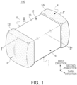
- FIG. 1 is a perspective diagram illustrating a multilayer electronic component according to an embodiment.
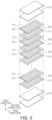
- FIG. 2 is an exploded perspective diagram illustrating a lamination structure of an internal electrode according to an embodiment.
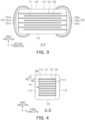
- FIG. 3 is a cross-sectional diagram taken along line I-I' in FIG. 1 .
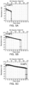
- FIG. 4 is a cross-sectional diagram taken along line II-II' in FIG. 1 .
- a multilayer ceramic capacitor will be described as an example of a multilayer electronic component, but an embodiment thereof is not limited thereto, and the multilayer ceramic capacitor may be applied to various multilayer electronic components, such as an inductor, a piezoelectric element, a varistor, or a thermistor.
- a multilayer electronic component 100 may include a body 110 including a dielectric layer 111 and internal electrodes 121 and 122; and external electrodes 131 and 132 disposed on the body 110, and may include a first sub-component including rare earth elements including at least one of yttrium (Y), dysprosium (Dy), or terbium (Tb), a second sub-component including silicon (Si), and a third sub-component including variable valence acceptor elements.
- Y yttrium
- Dy dysprosium
- Tb terbium
- Si silicon
- the multilayer electronic component 100 may include a body 110 including a dielectric layer 111 and internal electrodes 121 and 122; and external electrodes 131 and 132 disposed on the body 110, and the dielectric layer 111 may include a main component of a perovskite structure represented as ABO 3 and a sub-component, an A-site of the perovskite structure may include calcium (Ca) and strontium (Sr), and a B-site of the perovskite structure may include zirconium (Zr) and titanium (Ti), the sub-component may include a first sub-component including rare earth elements including at least one of yttrium (Y), dysprosium (Dy), or terbium (Tb), a second sub-component including silicon (Si), and a third sub-component including variable valence acceptor elements, and a content of the rare earth elements of the first sub-component may be 1.0 moles or higher and 2.0 moles or lower
- the body 110 may have the dielectric layers 111 and the internal electrodes 121 and 122 alternately laminated.
- the body 110 may include a capacitance forming portion Ac disposed in the body 110 and forming capacitance including the first internal electrode 121 and the second internal electrode 122 alternately disposed to face each other with the dielectric layer 111 interposed therebetween.
- the shape of the body 110 may not be limited to any particular shape, but as illustrated, the body 110 may have a hexahedral shape or a shape similar to a hexahedral shape. Due to reduction of ceramic powder included in the body 110 during a firing process, the body 110 may not have an exact hexahedral shape formed by linear lines but may have a substantially hexahedral shape.
- the body 110 may have first and second surfaces 1 and 2 opposing each other in the first direction, third and fourth surfaces 3 and 4 connected to the first and second surfaces 1 and 2 and opposing in the second direction, and fifth and sixth surfaces 5 and 6 connected to the first to fourth surfaces 1, 2, 3, and 4 and opposing each other in the third direction.
- the dissipation factor may also be referred to as dielectric loss and may be represented as loss tangent (tan ⁇ ).
- the definition of dissipation factor may refer to the time rate at which electrical energy is converted into heat in the dielectric when an electric field changing over time is applied.
- C0G properties may indicate C0G properties defined in the EIA standard, and may indicate the conditions in which, within the temperature range -55°C-125°C, a temperature coefficient ⁇ (10 -6 /K), which is the capacitance change rate, is 0, the temperature coefficient multiplier is -1, and the temperature coefficient tolerance is ⁇ 30ppm.
- COG properties may indicate the condition that 0 ⁇ 30ppm/°C is satisfied in the temperature range of -55°C-125°C.
- the dielectric layer 111 may include a first sub-component including rare earth elements as a sub-component, a second sub-component including silicon (Si), and a third sub-component including variable valence acceptor elements.
- various ceramic additives, organic solvents, binders, dispersants, or the like, may be added to the main component of CSZT in the embodiments.
- components may be analyzed using an EDS mode of a scanning electron microscope (SEM), an EDS mode of a transmission electron microscope (TEM), or an EDS mode of a scanning transmission electron microscope (STEM).
- SEM scanning electron microscope
- TEM transmission electron microscope
- STEM scanning transmission electron microscope
- a thinly sliced analysis sample may be prepared using focused ion beam (FIB) equipment in the region including a dielectric microstructure such as a dielectric grain in a cross-section of the dielectric material which has been sintered.
- FIB focused ion beam
- the damaged layer on the surface of the thinned sample may be removed using xenon (Xe) or argon (Ar) ion milling, and qualitative/quantitative analysis may be performed by mapping each component to be measured in the image obtained using SEM-EDS, TEM-EDS, or STEM-EDS.
- the qualitative/quantitative analysis graph of each component may be represented in terms of mass percentage (wt%), atomic percentage (at%), or moles percentage (mol%) of each element.
- the number of moles of a specific component may be represented by converting the number of moles of another specific component.
- the chip may be pulverized, the region including a dielectric microstructure may be selected, and the component in the region including a dielectric microstructure may be analyzed using devices such as inductively coupled plasma spectrometry (ICP-OES) and inductively coupled plasma mass spectrometry (ICP-MS).
- ICP-OES inductively coupled plasma spectrometry
- ICP-MS inductively coupled plasma mass spectrometry
- x may satisfy 0.5 ⁇ x ⁇ 1.0, y may satisfy 0.950 ⁇ y ⁇ 1.00. In some embodiments, ⁇ may satisfy 0.6 ⁇ x ⁇ 0.8, and y may satisfy 0.960 ⁇ y ⁇ 0.980. In some embodiments, x may be 0.7 and y may be 0.97.
- C0G properties may be satisfied.
- the sub-component may include the first sub-component including rare earth elements.
- a dielectric constant of C0G material including CSZT may be implemented by ion polarization, not dipole polarization. Accordingly, when rare earth elements are added to the C0G dielectric material, rare earth elements may increase interfacial resistance, thereby improving reliability, but when the elements are partially substituted or solid-solved into the lattice, the elements may act as a defect interfering with ion polarization, which has an adverse effect in terms of ion polarization. Accordingly, energy consumption required to implement the dielectric constant may increase, such that a dissipation factor may increase and a Q value may also decrease.
- the rare earth elements may include at least one of yttrium (Y), dysprosium (Dy), or terbium (Tb).
- the content of rare earth elements of the first sub-component may be 1.0 moles or higher and 2.0 moles or lower based on 100 moles of the CSZT main component, or may be 1.0 moles or higher and 2.0 moles or lower based on 100 moles of B-site of perovskite structure.
- the content of the rare earth elements of the first sub-component may satisfy 1.0 moles, 1.1 moles, 1.2 moles. 1.3 moles, 1.4 moles, 1.5 moles, 1.6 moles, 1.7 moles, 1.8 moles, 1.9 moles or higher and 2.0 moles, 1.9 moles, 1.8 moles, 1.7 moles, 1.6 moles, 1.5 moles, 1.4 moles, 1.3 moles, 1.2 moles, 1.1 moles or lower based on 100 moles of the CSZT main component, such that reliability of the multilayer electronic component may be improved.
- the Q value may decrease.
- the sub-component may include a second sub-component including silicon (Si).
- the second sub-component may act as a sintering aid, and may reduce the sintering temperature and facilitate sintering properties by reacting with the main component or other sub-components.
- the content of silicon (Si) of the second sub-component may be 0.95 moles or higher based on 100 moles of the CSZT main component, or may be 0.95 moles or higher based on 100 moles of the B-site of the perovskite structure.
- sintering density of the dielectric layer may be sufficiently implemented.
- the average sintering density of the dielectric layer may be implemented at 4.66g/cm 3 or more.
- An upper limit value of the content of silicon (Si) of the second sub-component is not limited to any particular example to sufficiently implement sintering density of the dielectric layer, and may be, for example, 1.35 moles or lower.
- sintering density may indicate bulk density among true density, apparent density, and bulk density, but the embodiment of the present disclosure is not limited thereto, and sintering density may indicate true density or apparent density, and there may be almost no difference in density values.
- Sintering density may be measured using, for example, a buoyancy-based Archimedes method. More specifically, the sintering density may be measured using an electron mirror, also used as a hydrometer, using the Archimedes principle, and when it is assumed that the density of water is 1, sintering density may be obtained by calculating the bulk density, which is one of the sintering densities.
- bulk density may be represented as ⁇ dry weight/(saturated weight-underwater weight) ⁇ , where dry weight is the weight of the sample in a state without water, underwater weight is the weight measured by suspending the sample in water, and saturated weight may be the weight measured after wiping only the surface of the sample immersed in water.
- the sintering density may be measured by measuring the weight (g) of the sample, measuring the size of the sample in the first direction, and calculating the volume by measuring the size in the second direction, and the size in the third direction.
- the method is not limited thereto.
- the sub-component may include a third sub-component including variable valence acceptor elements.
- variable valence acceptor elements may include at least one selected from the group consisting of manganese (Mn), vanadium (V), chromium (Cr), iron (Fe), cobalt (Co), nickel (Ni), copper (Cu), zinc (Zn), and combinations thereof, and may include manganese (Mn), but the embodiments of the present disclosure are not limited thereto.
- the content of the variable valence acceptor elements of the third sub-component may be 1.0 moles or higher 3.0 moles or lower based on 100 moles of the main component, or may be 1.0 moles or higher 3.0 moles or lower based on 100 moles of B-site of perovskite structure.
- the third sub-component may provide reduction resistance, may improve densification of the dielectric microstructure, and may maintain stable high temperature acceleration.
- variable valence acceptor elements of the third sub-component may satisfy 1.0 moles or higher 3.0 moles or lower based on 100 moles of the CSZT main component, reliability of the multilayer electronic component may be improved.
- variable valence acceptor elements of the third sub-component When the content of the variable valence acceptor elements of the third sub-component is less than 1.0 moles based on 100 moles of the CSZT main component, density may be reduced such that reliability may not be sufficient, and when the content of the third sub-component exceeds 3.0 moles based on 100 moles of the CSZT main component, the high temperature acceleration may deteriorate.
- the microstructure of the dielectric layer 111 of the multilayer electronic component may include a dielectric grain boundary disposed between a dielectric grain and a dielectric grain adjacent thereto.
- a resistance value of a grain boundary may be relatively larger than a resistance value in the grain.
- a resistance value of the grain boundary is greater than a resistance value in the grain may be explained by the Schottky barrier model in the interfacial region.
- a space charge layer having a high concentration of ions or electrons that is, a depletion layer, may be formed near the grain boundary.
- the Fermi level may increase, and the Schottky barrier height may increase, such that a depletion layer may increase.
- a thickness td of the dielectric layer 111 may not be limited to any particular example.
- the thickness of the dielectric layer 111 may be 10.0 ⁇ m or less. Also, to implement miniaturization and high capacitance of the multilayer electronic component 100, the thickness of the dielectric layer 111 may be 3.0 um or less. To more easily implement ultra-miniaturization and high capacitance, the thickness of the dielectric layer 111 may be 1.0 um or less, preferably 0.6 um or less, and more preferably 0.4 um or less.
- the thickness td of the dielectric layer 111 may refer to an average thickness of the dielectric layer 111 disposed between the first and second internal electrodes 121 and 122.
- the thickness td of the dielectric layer 111 may refer to the size of the dielectric layer 111 in the first direction. Also, the thickness td of the dielectric layer 111 may refer to the average thickness td of the dielectric layer 111 and may refer to the average size of the dielectric layer 111 in the first direction.
- the internal electrodes 121 and 122 may be alternately laminated with the dielectric layer 111.
- the internal electrodes may include a first internal electrode 121 and a second internal electrode 122.
- the first and second internal electrodes 121 and 122 may be alternately disposed to face each other with the dielectric layer 111 included in the body 110 interposed therebetween, and may be exposed to the third and fourth surfaces 3 and 4 of the body 110, respectively.
- first internal electrode 121 may be spaced apart from the fourth surface 4 and may be exposed through the third surface 3
- second internal electrode 122 may be spaced apart from the third surface 3 and may be exposed through the fourth surface 4.
- the first external electrode 131 may be disposed on the third surface 3 of the body 110 and may be connected to the first internal electrode 121
- the second external electrode 132 may be disposed on the fourth surface 4 of the body 110 and may be connected to the second internal electrode 122.
- first internal electrode 121 may not be connected to the second external electrode 132 and may be connected to the first external electrode 131
- the second internal electrode 122 may not be connected to the first external electrode 131 and may be connected to the second external electrode 132.
- the first and second internal electrodes 121 and 122 may be electrically separated from each other by the dielectric layer 111 disposed therebetween.
- the body 110 may be formed by alternately laminating ceramic green sheets on which the first internal electrodes 121 are printed and ceramic green sheets on which the second internal electrodes 122 are printed, and firing the sheets.
- the material for forming the internal electrodes 121 and 122 is not limited to any particular example, and any materials having excellent electrical conductivity may be used.
- the internal electrodes 121 and 122 may include one or more selected from the group consisting of nickel (Ni), copper (Cu), palladium (Pd), silver (Ag), gold (Au), platinum (Pt), tin (Sn), tungsten (W), titanium (Ti), and alloys thereof.
- the internal electrodes 121 and 122 may be formed by printing conductive paste for internal electrodes including one or more selected from the group consisting of nickel (Ni), copper (Cu), palladium (Pd), silver (Ag), gold (Au), platinum (Pt), tin (Sn), tungsten (W), titanium (Ti), and alloys thereof on a ceramic green sheet.
- a screenprinting method or a gravure printing method may be used as a method of printing the conductive paste for internal electrodes, but the disclosure of the present embodiment thereof is not limited thereto.
- the thickness te of the internal electrodes 121 and 122 may not be limited to any particular example.
- the thickness te of the internal electrodes 121 and 122 may be 3.0 ⁇ m or less. Also, to implement miniaturization and high capacitance of the multilayer electronic component 100, the thickness of the internal electrodes 121 and 122 may be 1.0 ⁇ m or less. To easily implement ultra-miniaturization and high capacitance, the thickness of the internal electrodes 121 and 122 may be 0.6 um or less, and according to some embodiment, 0.4 um or less.
- the thickness te of the internal electrodes 121 and 122 may refer to the size of the internal electrodes 121 and 122 in the first direction. Also, the thickness te of the internal electrodes 121 and 122 may refer to the average thickness te of the internal electrodes 121 and 122, and may refer to the average size of the internal electrodes 121 and 122 in the first direction.
- the average size of the internal electrodes 121 and 122 may be measured by scanning a cross-section of the body 110 in the first direction using a scanning electron microscope (SEM) with a magnification of 10,000. More specifically, an average value may be measured from the sizes of the internal electrode at 10 points at an equal distance in the second direction in the scanned image. The 10 points at an equal distance may be designated in the capacitance formation portion Ac. Also, by extending the measurement of the average value to 10 internal electrodes, the average size of the internal electrodes 121 and 122 may be further generalized.
- SEM scanning electron microscope
- the average thickness td of at least one of the plurality of dielectric layers 111 and the average thickness te of at least one of the plurality of internal electrodes 121 and 122 may satisfy 2 ⁇ te ⁇ td.
- the average thickness td of the dielectric layer 111 may be greater than twice the average thickness te of one of the internal electrodes 121 and 122.
- the average thickness td of the plurality of dielectric layers 111 may be greater than twice the average thickness te of the plurality of internal electrodes 121 and 122.
- a high-voltage electronic component may have an issue in reliability due to a decrease in breakdown voltage (BDV) in a high-voltage environment.
- BDV breakdown voltage
- the average thickness td of the dielectric layer 111 may be larger than twice the average thickness te of the internal electrodes 121 and 122, the thickness of the dielectric layer, which is the distance between the internal electrodes, may be increased and breakdown voltage properties may be improved.
- the average thickness td of the dielectric layer 111 is less than twice the average thickness te of the internal electrodes 121 and 122, the average thickness of the dielectric layer, which is the distance between the internal electrodes, may be reduced such that the breakdown voltage may decrease, and a short may occur between the internal electrodes.
- the body 110 may include cover portions 112 and 113 disposed on both end-surfaces in the first direction of the capacitance forming portion Ac.
- the body 110 may include a first cover portion 112 disposed on one surface in the first direction of the capacitance formation portion Ac and a second cover portion 113 disposed on the other surface in the first direction of the capacitance formation portion Ac. More specifically, the body 110 may include the upper cover portion 112 disposed in the upper portion in the first direction of the capacitance formation portion Ac and the lower cover portions 113 disposed in the lower portion in the first direction of the capacitance formation portion Ac.
- the upper cover portion 112 and the lower cover portion 113 may be formed by laminating a single dielectric layer 111 or two or more dielectric layers 111 on the upper and lower surfaces of the capacitance forming portion Ac in a first direction, and may prevent damages to the internal electrodes 121 and 122 due to physical or chemical stress.
- the upper cover portion 112 and the lower cover portion 113 may not include the internal electrodes 121 and 122 and may include the same material as that of the dielectric layer 111. That is, the upper cover portion 112 and the lower cover portion 113 may include a ceramic material, for example, a barium titanate (BaTiO 3 ) ceramic material.
- a ceramic material for example, a barium titanate (BaTiO 3 ) ceramic material.
- the thickness tc of the cover portion 112 and 113 may not need to be limited to any particular example.
- the thickness tc of the cover portions 112 and 113 may be 100 um or less, preferably 30 um or less. More preferably, the thickness may be 20 um or less in an ultra-small product.
- the thickness tc of the cover portion 112 or 113 may refer to the size in the first direction of the cover portion 112 or 113. Also, the thickness tc of the cover portions 112 and 113 may refer to the average thickness tc of the cover portions 112 and 113, and may refer to the average size in the first direction of the cover portions 112 and 113.
- the average size of the cover portions 112 and 113 may be measured by scanning a cross-section in the first and second directions of the body 110 using a scanning electron microscope (SEM) at a magnification of 10,000. More specifically, the average size may indicate the average value calculated by measuring the sizes in the first direction at 10 points at an equal distance in the second direction in the scanned image of the cover portion.
- SEM scanning electron microscope
- the average size in the first direction of the cover portion measured by the above method may be substantially the same as the average size in the first direction of the cover portion in the cross-section in the first and third directions of the body 110.
- the multilayer electronic component 100 may include side margin portions 114 and 115 disposed on both end-surfaces in the third direction of the body 110.
- the side margin portions 114 and 115 may include a first side margin portion 114 disposed on the fifth surface 5 and a second side margin portion 115 disposed on the sixth surface 6 of the body 110.
- the side margin portions 114 and 115 may refer to a region between both end-surfaces in the third direction of the first and second internal electrodes 121 and 122 and the boundary surface of the body 110 with respect to the cross-section in the first and third directions of the body 110.
- the side margin portions 114 and 115 may be formed by forming internal electrodes 121 and 122 on a ceramic green sheet by applying a conductive paste other than the region in which the side margin portions 114 and 115 are formed, cutting the laminated internal electrodes 121 and 122 to expose the fifth and sixth surfaces 5 and 6 of the body 110 to prevent a step difference caused by the internal electrodes 121 and 122, and laminating a single dielectric layer 111 or two or more dielectric layers 111 in the third direction on both end-surfaces in the third direction of the capacitance forming portion Ac.
- the side margin portions 114 and 115 may prevent damages to the internal electrodes 121 and 122 due to physical or chemical stress.
- the first side margin portion 114 and the second side margin portion 115 may not include the internal electrodes 121 and 122 and may include the same material as that of the dielectric layer 111. That is, the first side margin portion 114 and the second side margin portion 115 may include a ceramic material, for example, a barium titanate (BaTiO 3 ) ceramic material.
- a ceramic material for example, a barium titanate (BaTiO 3 ) ceramic material.
- the width wm of the first and second side margin portions 114 and 115 may not be limited to any particular example.
- the width wm of the side margin portions 114 and 115 may be 100 ⁇ m or less, preferably 30 um or less, and may be more preferably 20 ⁇ m or less in an ultra-small product.
- the width wm of the side margin portions 114 and 115 may refer to the size of the side margin portions 114 and 115 in the third direction. Also, the width wm of the side margin portions 114 and 115 may refer to the average width wm of the side margin portions 114 and 115, and the average size in the third direction of the side margin portions 114 and 115.
- the average size in the third direction of the side margin portion 114 and 115 may be measured by scanning a cross-section in the first and third directions of the body 110 using a scanning electron microscope (SEM) at a magnification of 10,000. More specifically, the average size may be an average value measured from the sizes in the third direction at 10 points at an equal distance in the first direction in the scanned image of one of the side margin portions.
- SEM scanning electron microscope
- the ceramic electronic component 100 may have two external electrodes 131 and 132, but the number of the external electrodes 131 and 132 or the shape thereof may be varied depending on the forms of the internal electrode 121 and 122 or other purposes.
- the external electrodes 131 and 132 may be disposed on the body 110 and may be connected to the internal electrodes 121 and 122.
- the external electrodes 131 and 132 may be disposed on the third and fourth surfaces 3 and 4 of the body 110, respectively, and may include first and second external electrodes 131 and 132 connected to the first and second internal electrodes 121 and 122, respectively. That is, the first external electrode 131 may be disposed on the third surface 3 of the body and may be connected to the first internal electrode 121, and the second external electrode 132 may be disposed on the fourth surface 4 of the body and may be connected to the second internal electrode 122.
- the external electrodes 131 and 132 may extend and be disposed on a portion of the first and second surfaces 1 and 2 of the body 110, or may extend and be disposed on a portion of the fifth and sixth surfaces 5 and 6 of the body 110. That is, the first external electrode 131 may be disposed on a portion of the first, second, fifth, and sixth surfaces 1, 2, 5, and 6 of the body 110, and the third surface 3 of the body 110, and the second external electrode 132 may be disposed on a portion of the first, second, fifth, and sixth surfaces 1, 2, 5, and 6 of the body 110, and the third surface 3 of the body 110.
- the external electrodes 131 and 132 may be formed of any materials having electrical conductivity, such as metal, and a specific material may be determined in consideration of electrical properties and structural stability, and the external electrodes 131 and 132 may have a multilayer structure.
- the external electrodes 131 and 132 may include an electrode layer disposed on the body 110 and a plating layer disposed on the electrode layer.
- the electrode layer may include first electrode layers 131a and 132a, which are fired electrodes including a first conductive metal and glass, or second electrode layers 131b and 132b, which are resin-based electrodes including second conductive metal and resin.
- the conductive metal included in the first electrode layers 131a and 132a may be referred to as a first conductive metal
- the conductive metal included in the second electrode layers 131b and 132b may be referred to as a second conductive metal.
- the first conductive metal and second conductive metal may be the same or different from each other, and when a plurality of conductive metals are included, only a portion thereof may include the same conductive metal, but an example embodiment thereof is not limited.
- first electrode layers 131a and 132a, and the second electrode layers 131b and 132b may be formed by disposing a fired electrode and a resin-based electrode on the body 110 in order.
- first electrode layers 131a and 132a, and the second electrode layers 131b and 132b may be formed by transferring a sheet including a conductive metal onto the body, and a sheet including a conductive metal onto the fired electrode.
- a material having excellent electrical conductivity may be used as a conductive metal included in the first electrode layers 131a and 132a, and the second electrode layers 131b and 132b.
- the conductive metal may include one or more selected from a group consisting of nickel (Ni), copper (Cu), palladium (Pd), silver (Ag), gold (Au), platinum (Pt), tin (Sn), tungsten (W), titanium (Ti) and alloys thereof, but an example embodiment thereof is not limited thereto.
- the electrode layers 131 and 132 may have a two-layer structure including the first electrode layers 131a and 132a and the second electrode layers 131b and 132b, and accordingly, the external electrodes 131 and 132 may include first electrode layers 131a and 132a including a first conductive metal and glass, and second electrode layers 131b and 132b disposed on the first electrode layers 131a and 132a and including a second conductive metal and resin.
- the first electrode layers 131a and 132a may improve bondability with the body 110 by including glass, and the second electrode layers 131b and 132b may improve warpage strength by including resin.
- the first conductive metal included in the first electrode layers 131a and 132a is not limited to any particular examples as long as the material may be electrically connected to the internal electrodes 121 and 122 to form capacitance, and for example, the first conductive metal may include one or more selected from the group consisting of nickel (Ni), copper (Cu), palladium (Pd), silver (Ag), gold (Au), platinum (Pt), tin (Sn), tungsten (W), titanium (Ti) and alloys thereof.
- the first electrode layers 131a and 132a may be formed by applying a conductive paste prepared by adding glass frit to the first conductive metal particles and firing the paste.
- the second conductive metal included in the second electrode layers 131b and 132b may allow the layers to be electrically connected to the first electrode layers 131a and 132a, respectively.
- the conductive metal included in the second electrode layers 131b and 132b is not limited to any particular example as long as the material may be electrically connected to the electrode layers 131a and 132a, and may include one or more selected from a group consisting of nickel (Ni), copper (Cu), palladium (Pd), silver (Ag), gold (Au), platinum (Pt), tin (Sn), tungsten (W), titanium (Ti) and alloys thereof.
- the second conductive metal included in the second electrode layers 131b and 132b may include one or more of spherical particles or flake-type particles.
- the conductive metal may only include flake-type particles, only spherical particles, or may be a mixture of flake-type particles and spherical particles.
- spherical particles may include shapes not completely spherical, for example, shapes in which the length ratio (major axis/minor axis) between the major axis and the minor axis is 1.45 or less.
- the flake-type particles may indicate particles having a flat and elongated shape, and are not limited to any particular example, and for example, the length ratio between the major axis and the minor axis (major axis/minor axis) may be 1.95 or more.
- the length of the major axis and the minor axis of the spherical particles and the flake-type particles may be measured from an image obtained by scanning the cross-sections in first and second direction of the central portion in the third direction of the multilayer electronic component using a scanning electron microscope (SEM).
- the resin included in the second electrode layers 131b and 132b may secure bondability and may absorb impacts.
- the resin included in the second electrode layers 131b and 132b is not limited to any particular examples as long as the resin has bondability and impact absorption properties and may be mixed with second conductive metal particles to create a paste, and may include, for example, an epoxy resin
- the second electrode layers 131b and 132b may include a plurality of metal particles, an intermetallic compound and a resin.
- an intermetallic compound By including an intermetallic compound, electrical connectivity with the first electrode layers 131a and 132a may be improved.
- the intermetallic compound may improve electrical connectivity by connecting a plurality of metal particles to each other, and may surround a plurality of metal particles and may connect the metal particles to each other.
- the intermetallic compound may include a metal having a melting point lower than a curing temperature of the resin. That is, as the intermetallic compound includes a metal having a melting point lower than the curing temperature of resin, the metal having a melting point lower than the curing temperature of the resin may melt during a drying and curing process, and may form an intermetallic compound with a portion of the metal particles and may surround the metal particles.
- the intermetallic compound may include a low melting point metal, preferably below 300°C.
- Sn having a melting point of 213-220°C may be included.
- Sn may be melted, and the melted Sn may wet metal particles at high melting points such as Ag, Ni, or Cu by capillary action, may react with a portion of Ag, Ni or Cu metal particles and may form intermetallic compounds such as Ag 3 Sn, Ni 3 Sn 4 , Cu 6 Sn 5 , or Cu 3 Sn.
- Ag, Ni or Cu not participating in the reaction may remain in the form of metal particles.
- the plurality of metal particles in the second electrode layers 131b and 132b may include one or more of Ag, Ni and Cu
- the intermetallic compound may include one or more of Ag 3 Sn, Ni 3 Sn 4 , Cu 6 Sn 5 and Cu 3 Sn.
- the plating layers 131c and 132c may improve mounting properties.
- the type of the plating layers 131c and 132c is not limited to any particular examples, and the plating layers 131c and 132c may be single-layer plating layers 131c and 132c including at least one selected from the group consisting of nickel (Ni), tin (Sn), palladium (Pd), and alloys thereof, and may be formed in a plurality of layers.
- the plating layers 131c and 132c may include Ni plating layers or Sn plating layers, and Ni plating layers and Sn plating layers may be formed in order on the electrode layers, and a Sn plating layer, a Ni plating layer, and a Sn plating layer may be formed in order.
- the plating layers 131c and 132c may include a plurality of Ni plating layers and/or a plurality of Sn plating layers.
- the size of the multilayer electronic component 100 may not be limited to any particular examples.
- the number of laminates may need to be increased by reducing the thickness of the dielectric layer and the internal electrode, such that the effect described in the embodiments may be noticeable in the multilayer electronic component 100 having a size of 3216 (length ⁇ width: 3.2mm ⁇ 1.6mm) or less.
- Table 1 lists Q values according to the type and content of rare earth elements, which are the first sub-component.
- the main component and other sub-components were added identically, other than the configuration in which the type and content of the first sub-component, rare earth elements, were applied differently.
- the content of the first to third sub-component was added based on 100 moles of the main component.
- Si silicon
- Mn manganese
- test examples 1-1 to 1-4 0.5 moles, 1.0 moles, 2.0 moles, and 2.6 moles of yttrium (Y) were added based on 100 moles of the CSZT main component, respectively, and in test examples 2-1 to 2-4, 0.5 moles, 1.0 moles, 2.0 moles, and 2.6 moles of dysprosium (Dy) were added based on 100 moles of the CSZT main component, respectively, and in test examples 3-1 to 3-4, 0.5 moles, 1.0 moles, 2.0 moles, and 2.6 moles of terbium (Tb) were added based on 100 moles of the CSZT main component, respectively.
- Y yttrium
- Dy dysprosium
- the Q values of the manufactured sample chips were measured, and when the Q value was 10,000 or more, the sample was evaluated as good and marked "O.” When the Q value was less than 10,000, the sample was evaluated as defective and marked "X.” The Q value was measured using 4268A of Keithley, an LCR meter measuring device. [Table 1] Test No.
- FIG. 5A is a STEP-IR graph of test example 1-1
- FIG. 5B is a STEP-IR graph of test example 1-2
- FIG. 5C is a STEP-IR graph of test example 1-3.
- FIG. 6A is a STEP-IR graph of test example 2-1
- FIG. 6B is a STEP-IR graph of test example 2-2
- FIG. 6C is a STEP-IR graph of test example 2-3.
- the STEP-IR test may determine whether a short of the chip appears under the harsh conditions in which the voltage increases by 10 V per 5 minutes at a temperature of 150°C, and may indicate whether reliability improves or deteriorates depending on the mean time to failure (MTTF).
- MTTF mean time to failure
- test examples 1-1 and 2-1 in which the content of rare earth elements was 0.5 moles, which is less than 1.0 moles, the mean time to failure (MTTF), which is the time when a chip short occurred relatively quickly, was short, which indicates that reliability deteriorated under the harsh conditions.
- MTTF mean time to failure
- test examples 1-2, 1-3, 2-2, and 2-3 in which the content of rare earth elements was 1.0 moles or higher and 2.0 moles or lower, as compared to test example 1-1 and 2-1, the mean time to failure (MTTF), which is the time when a short occurs in the chip, increased, indicating that reliability was excellent even under the harsh conditions.
- test example 1-1 to 1-3, 2-1 to 2-3 and 3-1 to 3-3 that, when the content of rare earth elements was 1.0 moles or higher and 2.0 moles or lower based on 100 moles of the CSZT main component, the Q value was excellent and reliability was also improved and accordingly, both the high-Q properties and reliability required for C0G material may be assured.
- the main component and the third sub-component were added identically, other than the configuration in which the content of the first sub-component, rare earth elements, and the second sub-component, silicon (Si), were applied differently.
- the content of the first to third sub-component was added based on 100 moles of the main component.
- test examples 4-1 to 4-4 1.0 moles of yttrium (Y) was added based on 100 moles of CSZT main component, and 0.75 moles, 0.95 moles, 1.15 moles, and 1.35 moles of silicon (Si) were added based on 100 moles of the CSZT main component, respectively.
- Y yttrium
- Si silicon
- test examples 5-1 to 5-4 2.0 moles of yttrium (Y) was added based on 100 moles of the CSZT main component, and 0.75 moles, 0.95 moles, 1.15 moles, and 1.35 moles of silicon (Si) were added based on 100 moles of the CSZT main component, respectively.
- Y yttrium
- Si silicon
- the average sintering density value (g/cm 3 ) for the manufactured sample chip was measured, and when the density was 4.56g/cm 3 or higher, which is more than 95% of the theoretical density of 4.8g/cm 3 for the CSZT dielectric material, the sample was evaluated as good and marked "O," and when the density was 4.56g/cm 3 , the sample was evaluated as defective and marked "X.” [Table 2] Test No.
- the average sintering density values were measured to be 4.53g/cm 3 and 4.52g/cm 3 , respectively, which indicates that sintering density was not excellent, such that the density of the dielectric microstructure deteriorated and the dielectric loss was relatively large.
- the average sintering density value was measured to be 4.66 g/cm 3 , which indicates that the sintering density was excellent, such that the dielectric microstructure density was excellent and the dielectric loss was relatively small.
- the content of silicon (Si) is 0.95 moles or higher based on 100 moles of the CSZT main component, it may be predicted that the average sintering density value may be excellent and the dielectric loss may be relatively small, and accordingly that high-Q properties required for C0G material may be assured.
- a multilayer electronic component may have a low equivalent series resistance (ESR).
- ESR equivalent series resistance
- a multilayer electronic component may have a high Q value.
- a multilayer electronic component may satisfy C0G properties.
- the term "embodiment” “embodiments” may not refer to one same embodiment, and may be provided to describe and emphasize different unique features of each embodiment.
- the suggested embodiments may be implemented do not exclude the possibilities of combination with features of other embodiments. For example, even though the features described in an embodiment are not described in the other embodiment, the description may be understood as relevant to the other embodiment unless otherwise indicated.
Landscapes
- Engineering & Computer Science (AREA)
- Power Engineering (AREA)
- Chemical & Material Sciences (AREA)
- Ceramic Engineering (AREA)
- Manufacturing & Machinery (AREA)
- Microelectronics & Electronic Packaging (AREA)
- Inorganic Chemistry (AREA)
- Structural Engineering (AREA)
- Organic Chemistry (AREA)
- Materials Engineering (AREA)
- Composite Materials (AREA)
- Fixed Capacitors And Capacitor Manufacturing Machines (AREA)
- Ceramic Capacitors (AREA)
Applications Claiming Priority (1)
| Application Number | Priority Date | Filing Date | Title |
|---|---|---|---|
| KR1020230161893A KR20250074931A (ko) | 2023-11-21 | 2023-11-21 | 적층형 전자 부품 |
Publications (2)
| Publication Number | Publication Date |
|---|---|
| EP4560663A2 true EP4560663A2 (de) | 2025-05-28 |
| EP4560663A3 EP4560663A3 (de) | 2025-07-16 |
Family
ID=93100378
Family Applications (1)
| Application Number | Title | Priority Date | Filing Date |
|---|---|---|---|
| EP24205770.1A Pending EP4560663A3 (de) | 2023-11-21 | 2024-10-10 | Mehrschichtiges elektronisches bauteil |
Country Status (5)
| Country | Link |
|---|---|
| US (1) | US20250166910A1 (de) |
| EP (1) | EP4560663A3 (de) |
| JP (1) | JP2025084068A (de) |
| KR (1) | KR20250074931A (de) |
| CN (1) | CN120032999A (de) |
Family Cites Families (5)
| Publication number | Priority date | Publication date | Assignee | Title |
|---|---|---|---|---|
| JP3924286B2 (ja) * | 2003-10-31 | 2007-06-06 | Tdk株式会社 | 積層セラミック電子部品の製造方法 |
| KR102333096B1 (ko) * | 2019-09-20 | 2021-12-01 | 삼성전기주식회사 | 유전체 조성물 및 이를 포함하는 적층형 전자 부품 |
| JP7279615B2 (ja) | 2019-11-05 | 2023-05-23 | 株式会社村田製作所 | 積層セラミックコンデンサ |
| CN116097382B (zh) * | 2020-09-10 | 2025-05-30 | 基美电子公司 | 谐振多层陶瓷电容器 |
| JP2022162546A (ja) * | 2021-04-12 | 2022-10-24 | 東ソー株式会社 | 焼結体 |
-
2023
- 2023-11-21 KR KR1020230161893A patent/KR20250074931A/ko active Pending
-
2024
- 2024-10-09 US US18/910,777 patent/US20250166910A1/en active Pending
- 2024-10-10 EP EP24205770.1A patent/EP4560663A3/de active Pending
- 2024-10-11 JP JP2024178570A patent/JP2025084068A/ja active Pending
- 2024-11-15 CN CN202411635441.9A patent/CN120032999A/zh active Pending
Also Published As
| Publication number | Publication date |
|---|---|
| JP2025084068A (ja) | 2025-06-02 |
| KR20250074931A (ko) | 2025-05-28 |
| US20250166910A1 (en) | 2025-05-22 |
| CN120032999A (zh) | 2025-05-23 |
| EP4560663A3 (de) | 2025-07-16 |
Similar Documents
| Publication | Publication Date | Title |
|---|---|---|
| US12327685B2 (en) | Multilayer electronic component | |
| KR102894865B1 (ko) | 세라믹 전자부품 | |
| EP4542598A1 (de) | Mehrschichtiges elektronisches bauteil | |
| EP4560663A2 (de) | Mehrschichtiges elektronisches bauteil | |
| EP4557333A1 (de) | Mehrschichtiger keramik kondensator | |
| EP4557332A1 (de) | Mehrschichtiger keramischer kondensator | |
| EP4576141A1 (de) | Mehrschichtiges elektronisches bauteil | |
| EP4557337A2 (de) | Mehrschichtiges elektronisches bauelement mit barium, gallium und zinn in den dielektrischen deckschichten | |
| EP4564388A1 (de) | Mehrschichtiges elektronischer kondensator | |
| EP4576140A1 (de) | Mehrschichtiges elektronisches bauteil | |
| EP4513519A2 (de) | Umhüllung eines mehrschichtigen elektronischen bauelements mit perowskit-struktur (abo3) mit einem ersten metall auf der basis von cu, w, ag und zn | |
| EP4557335A2 (de) | Mehrschichtiges elektronisches bauteil | |
| EP4451300A2 (de) | Mehrschichtiges elektronisches bauteil | |
| EP4560665A1 (de) | Mehrschichtiger keramik kondensator | |
| EP4421834A2 (de) | Mehrschichtiges elektronisches bauteil | |
| EP4546383A1 (de) | Mehrschichtiges elektronisches bauteil | |
| US20260038740A1 (en) | Multilayer electronic component | |
| EP4435811A2 (de) | Mehrschichtiges elektronisches bauteil | |
| US20250182974A1 (en) | Multilayer electronic component | |
| EP4560664A2 (de) | Äussere elektroden für ein mehrschichtiges keramisches bauteil mit einer schicht aus borosilikatglas an seinem oberen und unteren ende | |
| EP4425513A1 (de) | Molarverhältnis von ba ti und si in den dielektrischen schichten für mehrschichtige keramische komponenten | |
| US20230207194A1 (en) | Multilayer ceramic electronic component | |
| US20250079084A1 (en) | Dielectric composition and multilayered capacitor containing the same | |
| EP4216246A1 (de) | Mehrschichtiges elektronisches bauteil | |
| KR20240164342A (ko) | 적층형 전자 부품 |
Legal Events
| Date | Code | Title | Description |
|---|---|---|---|
| PUAI | Public reference made under article 153(3) epc to a published international application that has entered the european phase |
Free format text: ORIGINAL CODE: 0009012 |
|
| STAA | Information on the status of an ep patent application or granted ep patent |
Free format text: STATUS: THE APPLICATION HAS BEEN PUBLISHED |
|
| AK | Designated contracting states |
Kind code of ref document: A2 Designated state(s): AL AT BE BG CH CY CZ DE DK EE ES FI FR GB GR HR HU IE IS IT LI LT LU LV MC ME MK MT NL NO PL PT RO RS SE SI SK SM TR |
|
| PUAL | Search report despatched |
Free format text: ORIGINAL CODE: 0009013 |
|
| AK | Designated contracting states |
Kind code of ref document: A3 Designated state(s): AL AT BE BG CH CY CZ DE DK EE ES FI FR GB GR HR HU IE IS IT LI LT LU LV MC ME MK MT NL NO PL PT RO RS SE SI SK SM TR |
|
| RIC1 | Information provided on ipc code assigned before grant |
Ipc: H01G 4/12 20060101AFI20250611BHEP Ipc: H01G 4/30 20060101ALI20250611BHEP Ipc: C04B 35/468 20060101ALI20250611BHEP Ipc: C04B 35/465 20060101ALN20250611BHEP Ipc: C04B 35/462 20060101ALN20250611BHEP |
|
| STAA | Information on the status of an ep patent application or granted ep patent |
Free format text: STATUS: REQUEST FOR EXAMINATION WAS MADE |
|
| 17P | Request for examination filed |
Effective date: 20251030 |