EP4576141A1 - Mehrschichtiges elektronisches bauteil - Google Patents
Mehrschichtiges elektronisches bauteil Download PDFInfo
- Publication number
- EP4576141A1 EP4576141A1 EP24216081.0A EP24216081A EP4576141A1 EP 4576141 A1 EP4576141 A1 EP 4576141A1 EP 24216081 A EP24216081 A EP 24216081A EP 4576141 A1 EP4576141 A1 EP 4576141A1
- Authority
- EP
- European Patent Office
- Prior art keywords
- secondary phase
- mol
- phase grains
- subcomponent
- dielectric layer
- Prior art date
- Legal status (The legal status is an assumption and is not a legal conclusion. Google has not performed a legal analysis and makes no representation as to the accuracy of the status listed.)
- Pending
Links
Images


Classifications
-
- H—ELECTRICITY
- H01—ELECTRIC ELEMENTS
- H01G—CAPACITORS; CAPACITORS, RECTIFIERS, DETECTORS, SWITCHING DEVICES, LIGHT-SENSITIVE OR TEMPERATURE-SENSITIVE DEVICES OF THE ELECTROLYTIC TYPE
- H01G4/00—Fixed capacitors; Processes of their manufacture
- H01G4/002—Details
- H01G4/018—Dielectrics
- H01G4/06—Solid dielectrics
- H01G4/08—Inorganic dielectrics
- H01G4/12—Ceramic dielectrics
- H01G4/1209—Ceramic dielectrics characterised by the ceramic dielectric material
- H01G4/1218—Ceramic dielectrics characterised by the ceramic dielectric material based on titanium oxides or titanates
- H01G4/1227—Ceramic dielectrics characterised by the ceramic dielectric material based on titanium oxides or titanates based on alkaline earth titanates
-
- C—CHEMISTRY; METALLURGY
- C04—CEMENTS; CONCRETE; ARTIFICIAL STONE; CERAMICS; REFRACTORIES
- C04B—LIME, MAGNESIA; SLAG; CEMENTS; COMPOSITIONS THEREOF, e.g. MORTARS, CONCRETE OR LIKE BUILDING MATERIALS; ARTIFICIAL STONE; CERAMICS; REFRACTORIES; TREATMENT OF NATURAL STONE
- C04B35/00—Shaped ceramic products characterised by their composition; Ceramics compositions; Processing powders of inorganic compounds preparatory to the manufacturing of ceramic products
- C04B35/01—Shaped ceramic products characterised by their composition; Ceramics compositions; Processing powders of inorganic compounds preparatory to the manufacturing of ceramic products based on oxide ceramics
- C04B35/46—Shaped ceramic products characterised by their composition; Ceramics compositions; Processing powders of inorganic compounds preparatory to the manufacturing of ceramic products based on oxide ceramics based on titanium oxides or titanates
- C04B35/462—Shaped ceramic products characterised by their composition; Ceramics compositions; Processing powders of inorganic compounds preparatory to the manufacturing of ceramic products based on oxide ceramics based on titanium oxides or titanates based on titanates
- C04B35/465—Shaped ceramic products characterised by their composition; Ceramics compositions; Processing powders of inorganic compounds preparatory to the manufacturing of ceramic products based on oxide ceramics based on titanium oxides or titanates based on titanates based on alkaline earth metal titanates
- C04B35/468—Shaped ceramic products characterised by their composition; Ceramics compositions; Processing powders of inorganic compounds preparatory to the manufacturing of ceramic products based on oxide ceramics based on titanium oxides or titanates based on titanates based on alkaline earth metal titanates based on barium titanates
- C04B35/4682—Shaped ceramic products characterised by their composition; Ceramics compositions; Processing powders of inorganic compounds preparatory to the manufacturing of ceramic products based on oxide ceramics based on titanium oxides or titanates based on titanates based on alkaline earth metal titanates based on barium titanates based on BaTiO3 perovskite phase
-
- C—CHEMISTRY; METALLURGY
- C04—CEMENTS; CONCRETE; ARTIFICIAL STONE; CERAMICS; REFRACTORIES
- C04B—LIME, MAGNESIA; SLAG; CEMENTS; COMPOSITIONS THEREOF, e.g. MORTARS, CONCRETE OR LIKE BUILDING MATERIALS; ARTIFICIAL STONE; CERAMICS; REFRACTORIES; TREATMENT OF NATURAL STONE
- C04B35/00—Shaped ceramic products characterised by their composition; Ceramics compositions; Processing powders of inorganic compounds preparatory to the manufacturing of ceramic products
- C04B35/622—Forming processes; Processing powders of inorganic compounds preparatory to the manufacturing of ceramic products
- C04B35/64—Burning or sintering processes
-
- H—ELECTRICITY
- H01—ELECTRIC ELEMENTS
- H01G—CAPACITORS; CAPACITORS, RECTIFIERS, DETECTORS, SWITCHING DEVICES, LIGHT-SENSITIVE OR TEMPERATURE-SENSITIVE DEVICES OF THE ELECTROLYTIC TYPE
- H01G4/00—Fixed capacitors; Processes of their manufacture
- H01G4/002—Details
- H01G4/005—Electrodes
-
- H—ELECTRICITY
- H01—ELECTRIC ELEMENTS
- H01G—CAPACITORS; CAPACITORS, RECTIFIERS, DETECTORS, SWITCHING DEVICES, LIGHT-SENSITIVE OR TEMPERATURE-SENSITIVE DEVICES OF THE ELECTROLYTIC TYPE
- H01G4/00—Fixed capacitors; Processes of their manufacture
- H01G4/002—Details
- H01G4/005—Electrodes
- H01G4/008—Selection of materials
-
- H—ELECTRICITY
- H01—ELECTRIC ELEMENTS
- H01G—CAPACITORS; CAPACITORS, RECTIFIERS, DETECTORS, SWITCHING DEVICES, LIGHT-SENSITIVE OR TEMPERATURE-SENSITIVE DEVICES OF THE ELECTROLYTIC TYPE
- H01G4/00—Fixed capacitors; Processes of their manufacture
- H01G4/002—Details
- H01G4/005—Electrodes
- H01G4/012—Form of non-self-supporting electrodes
-
- H—ELECTRICITY
- H01—ELECTRIC ELEMENTS
- H01G—CAPACITORS; CAPACITORS, RECTIFIERS, DETECTORS, SWITCHING DEVICES, LIGHT-SENSITIVE OR TEMPERATURE-SENSITIVE DEVICES OF THE ELECTROLYTIC TYPE
- H01G4/00—Fixed capacitors; Processes of their manufacture
- H01G4/30—Stacked capacitors
-
- C—CHEMISTRY; METALLURGY
- C04—CEMENTS; CONCRETE; ARTIFICIAL STONE; CERAMICS; REFRACTORIES
- C04B—LIME, MAGNESIA; SLAG; CEMENTS; COMPOSITIONS THEREOF, e.g. MORTARS, CONCRETE OR LIKE BUILDING MATERIALS; ARTIFICIAL STONE; CERAMICS; REFRACTORIES; TREATMENT OF NATURAL STONE
- C04B2235/00—Aspects relating to ceramic starting mixtures or sintered ceramic products
- C04B2235/02—Composition of constituents of the starting material or of secondary phases of the final product
- C04B2235/30—Constituents and secondary phases not being of a fibrous nature
- C04B2235/32—Metal oxides, mixed metal oxides, or oxide-forming salts thereof, e.g. carbonates, nitrates, (oxy)hydroxides, chlorides
- C04B2235/3205—Alkaline earth oxides or oxide forming salts thereof, e.g. beryllium oxide
- C04B2235/3206—Magnesium oxides or oxide-forming salts thereof
-
- C—CHEMISTRY; METALLURGY
- C04—CEMENTS; CONCRETE; ARTIFICIAL STONE; CERAMICS; REFRACTORIES
- C04B—LIME, MAGNESIA; SLAG; CEMENTS; COMPOSITIONS THEREOF, e.g. MORTARS, CONCRETE OR LIKE BUILDING MATERIALS; ARTIFICIAL STONE; CERAMICS; REFRACTORIES; TREATMENT OF NATURAL STONE
- C04B2235/00—Aspects relating to ceramic starting mixtures or sintered ceramic products
- C04B2235/02—Composition of constituents of the starting material or of secondary phases of the final product
- C04B2235/30—Constituents and secondary phases not being of a fibrous nature
- C04B2235/32—Metal oxides, mixed metal oxides, or oxide-forming salts thereof, e.g. carbonates, nitrates, (oxy)hydroxides, chlorides
- C04B2235/3205—Alkaline earth oxides or oxide forming salts thereof, e.g. beryllium oxide
- C04B2235/3215—Barium oxides or oxide-forming salts thereof
-
- C—CHEMISTRY; METALLURGY
- C04—CEMENTS; CONCRETE; ARTIFICIAL STONE; CERAMICS; REFRACTORIES
- C04B—LIME, MAGNESIA; SLAG; CEMENTS; COMPOSITIONS THEREOF, e.g. MORTARS, CONCRETE OR LIKE BUILDING MATERIALS; ARTIFICIAL STONE; CERAMICS; REFRACTORIES; TREATMENT OF NATURAL STONE
- C04B2235/00—Aspects relating to ceramic starting mixtures or sintered ceramic products
- C04B2235/02—Composition of constituents of the starting material or of secondary phases of the final product
- C04B2235/30—Constituents and secondary phases not being of a fibrous nature
- C04B2235/32—Metal oxides, mixed metal oxides, or oxide-forming salts thereof, e.g. carbonates, nitrates, (oxy)hydroxides, chlorides
- C04B2235/3224—Rare earth oxide or oxide forming salts thereof, e.g. scandium oxide
-
- C—CHEMISTRY; METALLURGY
- C04—CEMENTS; CONCRETE; ARTIFICIAL STONE; CERAMICS; REFRACTORIES
- C04B—LIME, MAGNESIA; SLAG; CEMENTS; COMPOSITIONS THEREOF, e.g. MORTARS, CONCRETE OR LIKE BUILDING MATERIALS; ARTIFICIAL STONE; CERAMICS; REFRACTORIES; TREATMENT OF NATURAL STONE
- C04B2235/00—Aspects relating to ceramic starting mixtures or sintered ceramic products
- C04B2235/02—Composition of constituents of the starting material or of secondary phases of the final product
- C04B2235/30—Constituents and secondary phases not being of a fibrous nature
- C04B2235/32—Metal oxides, mixed metal oxides, or oxide-forming salts thereof, e.g. carbonates, nitrates, (oxy)hydroxides, chlorides
- C04B2235/3231—Refractory metal oxides, their mixed metal oxides, or oxide-forming salts thereof
- C04B2235/3232—Titanium oxides or titanates, e.g. rutile or anatase
-
- C—CHEMISTRY; METALLURGY
- C04—CEMENTS; CONCRETE; ARTIFICIAL STONE; CERAMICS; REFRACTORIES
- C04B—LIME, MAGNESIA; SLAG; CEMENTS; COMPOSITIONS THEREOF, e.g. MORTARS, CONCRETE OR LIKE BUILDING MATERIALS; ARTIFICIAL STONE; CERAMICS; REFRACTORIES; TREATMENT OF NATURAL STONE
- C04B2235/00—Aspects relating to ceramic starting mixtures or sintered ceramic products
- C04B2235/02—Composition of constituents of the starting material or of secondary phases of the final product
- C04B2235/30—Constituents and secondary phases not being of a fibrous nature
- C04B2235/32—Metal oxides, mixed metal oxides, or oxide-forming salts thereof, e.g. carbonates, nitrates, (oxy)hydroxides, chlorides
- C04B2235/3231—Refractory metal oxides, their mixed metal oxides, or oxide-forming salts thereof
- C04B2235/3239—Vanadium oxides, vanadates or oxide forming salts thereof, e.g. magnesium vanadate
-
- C—CHEMISTRY; METALLURGY
- C04—CEMENTS; CONCRETE; ARTIFICIAL STONE; CERAMICS; REFRACTORIES
- C04B—LIME, MAGNESIA; SLAG; CEMENTS; COMPOSITIONS THEREOF, e.g. MORTARS, CONCRETE OR LIKE BUILDING MATERIALS; ARTIFICIAL STONE; CERAMICS; REFRACTORIES; TREATMENT OF NATURAL STONE
- C04B2235/00—Aspects relating to ceramic starting mixtures or sintered ceramic products
- C04B2235/02—Composition of constituents of the starting material or of secondary phases of the final product
- C04B2235/30—Constituents and secondary phases not being of a fibrous nature
- C04B2235/32—Metal oxides, mixed metal oxides, or oxide-forming salts thereof, e.g. carbonates, nitrates, (oxy)hydroxides, chlorides
- C04B2235/3262—Manganese oxides, manganates, rhenium oxides or oxide-forming salts thereof, e.g. MnO
-
- C—CHEMISTRY; METALLURGY
- C04—CEMENTS; CONCRETE; ARTIFICIAL STONE; CERAMICS; REFRACTORIES
- C04B—LIME, MAGNESIA; SLAG; CEMENTS; COMPOSITIONS THEREOF, e.g. MORTARS, CONCRETE OR LIKE BUILDING MATERIALS; ARTIFICIAL STONE; CERAMICS; REFRACTORIES; TREATMENT OF NATURAL STONE
- C04B2235/00—Aspects relating to ceramic starting mixtures or sintered ceramic products
- C04B2235/02—Composition of constituents of the starting material or of secondary phases of the final product
- C04B2235/30—Constituents and secondary phases not being of a fibrous nature
- C04B2235/34—Non-metal oxides, non-metal mixed oxides, or salts thereof that form the non-metal oxides upon heating, e.g. carbonates, nitrates, (oxy)hydroxides, chlorides
- C04B2235/3418—Silicon oxide, silicic acids or oxide forming salts thereof, e.g. silica sol, fused silica, silica fume, cristobalite, quartz or flint
-
- C—CHEMISTRY; METALLURGY
- C04—CEMENTS; CONCRETE; ARTIFICIAL STONE; CERAMICS; REFRACTORIES
- C04B—LIME, MAGNESIA; SLAG; CEMENTS; COMPOSITIONS THEREOF, e.g. MORTARS, CONCRETE OR LIKE BUILDING MATERIALS; ARTIFICIAL STONE; CERAMICS; REFRACTORIES; TREATMENT OF NATURAL STONE
- C04B2235/00—Aspects relating to ceramic starting mixtures or sintered ceramic products
- C04B2235/02—Composition of constituents of the starting material or of secondary phases of the final product
- C04B2235/30—Constituents and secondary phases not being of a fibrous nature
- C04B2235/34—Non-metal oxides, non-metal mixed oxides, or salts thereof that form the non-metal oxides upon heating, e.g. carbonates, nitrates, (oxy)hydroxides, chlorides
- C04B2235/3427—Silicates other than clay, e.g. water glass
-
- C—CHEMISTRY; METALLURGY
- C04—CEMENTS; CONCRETE; ARTIFICIAL STONE; CERAMICS; REFRACTORIES
- C04B—LIME, MAGNESIA; SLAG; CEMENTS; COMPOSITIONS THEREOF, e.g. MORTARS, CONCRETE OR LIKE BUILDING MATERIALS; ARTIFICIAL STONE; CERAMICS; REFRACTORIES; TREATMENT OF NATURAL STONE
- C04B2235/00—Aspects relating to ceramic starting mixtures or sintered ceramic products
- C04B2235/02—Composition of constituents of the starting material or of secondary phases of the final product
- C04B2235/50—Constituents or additives of the starting mixture chosen for their shape or used because of their shape or their physical appearance
- C04B2235/54—Particle size related information
- C04B2235/5418—Particle size related information expressed by the size of the particles or aggregates thereof
- C04B2235/5445—Particle size related information expressed by the size of the particles or aggregates thereof submicron sized, i.e. from 0,1 to 1 micron
-
- C—CHEMISTRY; METALLURGY
- C04—CEMENTS; CONCRETE; ARTIFICIAL STONE; CERAMICS; REFRACTORIES
- C04B—LIME, MAGNESIA; SLAG; CEMENTS; COMPOSITIONS THEREOF, e.g. MORTARS, CONCRETE OR LIKE BUILDING MATERIALS; ARTIFICIAL STONE; CERAMICS; REFRACTORIES; TREATMENT OF NATURAL STONE
- C04B2235/00—Aspects relating to ceramic starting mixtures or sintered ceramic products
- C04B2235/65—Aspects relating to heat treatments of ceramic bodies such as green ceramics or pre-sintered ceramics, e.g. burning, sintering or melting processes
- C04B2235/656—Aspects relating to heat treatments of ceramic bodies such as green ceramics or pre-sintered ceramics, e.g. burning, sintering or melting processes characterised by specific heating conditions during heat treatment
- C04B2235/6567—Treatment time
-
- C—CHEMISTRY; METALLURGY
- C04—CEMENTS; CONCRETE; ARTIFICIAL STONE; CERAMICS; REFRACTORIES
- C04B—LIME, MAGNESIA; SLAG; CEMENTS; COMPOSITIONS THEREOF, e.g. MORTARS, CONCRETE OR LIKE BUILDING MATERIALS; ARTIFICIAL STONE; CERAMICS; REFRACTORIES; TREATMENT OF NATURAL STONE
- C04B2235/00—Aspects relating to ceramic starting mixtures or sintered ceramic products
- C04B2235/65—Aspects relating to heat treatments of ceramic bodies such as green ceramics or pre-sintered ceramics, e.g. burning, sintering or melting processes
- C04B2235/658—Atmosphere during thermal treatment
- C04B2235/6582—Hydrogen containing atmosphere
-
- C—CHEMISTRY; METALLURGY
- C04—CEMENTS; CONCRETE; ARTIFICIAL STONE; CERAMICS; REFRACTORIES
- C04B—LIME, MAGNESIA; SLAG; CEMENTS; COMPOSITIONS THEREOF, e.g. MORTARS, CONCRETE OR LIKE BUILDING MATERIALS; ARTIFICIAL STONE; CERAMICS; REFRACTORIES; TREATMENT OF NATURAL STONE
- C04B2235/00—Aspects relating to ceramic starting mixtures or sintered ceramic products
- C04B2235/70—Aspects relating to sintered or melt-casted ceramic products
- C04B2235/80—Phases present in the sintered or melt-cast ceramic products other than the main phase
- C04B2235/85—Intergranular or grain boundary phases
-
- H—ELECTRICITY
- H01—ELECTRIC ELEMENTS
- H01G—CAPACITORS; CAPACITORS, RECTIFIERS, DETECTORS, SWITCHING DEVICES, LIGHT-SENSITIVE OR TEMPERATURE-SENSITIVE DEVICES OF THE ELECTROLYTIC TYPE
- H01G4/00—Fixed capacitors; Processes of their manufacture
- H01G4/002—Details
- H01G4/018—Dielectrics
- H01G4/06—Solid dielectrics
- H01G4/08—Inorganic dielectrics
- H01G4/12—Ceramic dielectrics
- H01G4/1209—Ceramic dielectrics characterised by the ceramic dielectric material
Definitions
- the present disclosure relates to a multilayer electronic component.
- a multilayer ceramic capacitor (MLCC), a multilayer electronic component, is a chip-type condenser, mounted on the printed circuit boards of various types of electronic product, such as image display devices including a liquid crystal display (LCD) and a plasma display panel (PDP), computers, smartphones and mobile phones, and serves to charge or discharge electricity therein or therefrom.
- image display devices including a liquid crystal display (LCD) and a plasma display panel (PDP)
- LCD liquid crystal display
- PDP plasma display panel
- the multilayer ceramic capacitor may be used as a component in various electronic devices due to having a small size, ensuring high capacitance and being easily mounted.
- miniaturization and implementation of high output power of various electronic devices such as computers and mobile devices
- demand for miniaturization and high capacitance of multilayer ceramic capacitors has also been increasing.
- Existing high-capacitance multilayer electronic components are materials sintered by adding fixed valence acceptors such as magnesium (Mg), aluminum (Al), and the like, and adding rare earth elements serving as a donor, or adding variable valence acceptors such as manganese (Mn), vanadium (V), chromium (Cr), and the like, while also adding sintering aids such as barium (Ba) or silicon (Si).
- fixed valence acceptors such as magnesium (Mg), aluminum (Al), and the like
- rare earth elements serving as a donor or adding variable valence acceptors such as manganese (Mn), vanadium (V), chromium (Cr), and the like
- sintering aids such as barium (Ba) or silicon (Si).
- doping of additional elements is required, and as in the past, it is a desirable direction to additionally add rare earth elements whose main purpose is to improve reliability.
- some rare earth elements may form a barium titanate (BaTiO 3 )-based crystal lattice and core-shell structure, thereby realizing further improved reliability.
- some rare earth elements do not participate in shell formation through solid solution in the crystal lattice of barium titanate (BaTiO 3 ), but combine with other elements to form a secondary phase, and cases in which the formed secondary-phase does not affect reliability or rather has a negative effect have been found, and thus, control of the secondary-phase is required.
- An aspect of the present disclosure is to provide a multilayer electronic component having improved reliability.
- An aspect of the present disclosure is to provide a multilayer electronic component satisfying X7R or X7S characteristics.
- An aspect of the present disclosure is to provide a multilayer electronic component having improved MTTF of high temperature and high pressure acceleration lifespan.
- An aspect of the present disclosure is to provide a multilayer electronic component having improved capacitance.
- a multilayer electronic component may include: a body including a capacitance formation portion including a dielectric layer and an internal electrode; and an external electrode disposed on the body, and when secondary phase grains including rare earth elements and titanium (Ti) are referred to as first secondary phase grains and secondary phase grains including the rare earth elements and silicon (Si) are referred to as second secondary phase grains, and when the number of the first secondary phase grains included in the capacitance formation portion is referred to as A and the number of the second secondary phase grains included in the capacitance formation portion is referred to as B, the capacitance formation portion may satisfy 0 ⁇ A/(A+B) ⁇ 0.4.
- a multilayer electronic component may include: a body including a capacitance formation portion including a dielectric layer and an internal electrode; and an external electrode disposed on the body, and when secondary phase grains including rare earth elements and titanium (Ti) are referred to as first secondary phase grains and secondary phase grains including the rare earth elements and silicon (Si) are referred to as second secondary phase grains, and when the number of the first secondary phase grains included in the capacitance formation portion is referred to as A and the number of the second secondary phase grains included in the capacitance formation portion is referred to as B, the capacitance formation portion may satisfy 0 ⁇ A and 0 ⁇ B.
- One of the various effects of the present disclosure is to improve the reliability of a multilayer electronic component.
- One of the various effects of the present disclosure is to satisfy the X7R or X7S characteristics of a multilayer electronic component.
- One of the various effects of the present disclosure is to improve the MTTF of the high temperature and high pressure accelerated lifespan of a multilayer electronic component.
- One of the various effects of the present disclosure is to improve the capacitance of a multilayer electronic component.
- a first direction may be defined as a thickness T direction
- a second direction may be defined as a length L direction
- a third direction may be defined as a width W direction.
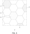
- FIG. 1 schematically illustrates a perspective view of a multilayer electronic component according to an example embodiment of the present disclosure.
- a multilayer electronic component 100 may include a body 110 including a capacitance formation portion Ac including a dielectric layer 111 and internal electrodes 121 and 122; and external electrodes 131 and 132 disposed on the body 110, and when secondary phase grains including rare earth elements and titanium (Ti) are referred to as first secondary phase grains 10 and secondary phase grains including the rare earth elements and silicon (Si) are referred to as second secondary phase grains 20, and when the number of the first secondary phase grains 10 included in the capacitance formation portion Ac is referred to as A and the number of the second secondary phase grains 20 included in the capacitance formation portion Ac is referred to as B, the capacitance formation portion Ac may satisfy 0 ⁇ A/(A+B) ⁇ 0.4.
- a multilayer electronic component 100 may include a body 110 including a capacitance formation portion Ac including a dielectric layer 111 and internal electrodes 121 and 122; and external electrodes 131 and 132 disposed on the body 110, and when secondary phase grains including rare earth elements and titanium (Ti) are referred to as first secondary phase grains 10 and secondary phase grains including the rare earth elements and silicon (Si) are referred to as second secondary phase grains 20, and when the number of the first secondary phase grains 10 included in the capacitance formation portion Ac is referred to as A and the number of the second secondary phase grains 20 included in the capacitance formation portion Ac is referred to as B, the capacitance formation portion Ac may satisfy 0 ⁇ A and 0 ⁇ B.
- the body 110 may include dielectric layers 111 and internal electrodes 121 and 122 alternately stacked.
- the body 110 may include a capacitance formation portion Ac disposed inside the body 110, and including first internal electrodes 121 and second internal electrodes 122 alternately arranged to face each other with the dielectric layer 111 interposed therebetween to form capacitance.
- the body 110 may have first and second surfaces 1 and 2 opposing each other in the first direction, third and fourth surfaces 3 and 4 connected to the first and second surfaces 1 and 2 and opposing each other in the second direction, and fifth and sixth surfaces 5 and 6 connected to the first to fourth surfaces 1, 2, 3 and 4 and opposing each other in the third direction.
- the barium titanate-based material may include BaTiO 3 -based ceramic particles, and examples of ceramic particles may include BaTiO 3 , and (Ba 1-x Ca x )TiO 3 (0 ⁇ x ⁇ 1), Ba(Ti x-y Ca y )O 3 (0 ⁇ y ⁇ 1), (Ba 1-x Ca x )(Ti 1-y Zr y )O 3 (0 ⁇ x ⁇ 1, 0 ⁇ y ⁇ 1) or Ba(Ti 1-y Zr y )O 3 (0 ⁇ y ⁇ 1), which is formed by partially employing calcium (Ca) and zirconium (Zr) in BaTiO 3 .
- ceramic particles may include BaTiO 3 , and (Ba 1-x Ca x )TiO 3 (0 ⁇ x ⁇ 1), Ba(Ti x-y Ca y )O 3 (0 ⁇ y ⁇ 1), (Ba 1-x Ca x )(Ti 1-y Zr y )O 3 (0 ⁇ x ⁇ 1, 0 ⁇ y ⁇ 1) or Ba(T
- various ceramic additives, organic solvents, binders, dispersants, and the like may be added to particles such as barium titanate (BaTiO 3 ) according to the purpose of the present disclosure.
- the rare earth elements added in excessive amounts may adjust a ratio of the number (A) of first secondary phase grains 10 generated by combining rare earth elements and titanium (Ti) and the number B of second secondary phase grains 20 generated by combining the rare earth elements with silicon (Si), in addition to the core-shell structure, thereby achieving high reliability.
- the capacitance formation portion Ac may satisfy 0 ⁇ A/(A+B) ⁇ 0.4.
- the capacitance formation portion Ac may include a cross-sectional area of 1.85 um ⁇ 1.85 um satisfying a condition 0 ⁇ A/(A+B) ⁇ 0.4, and in the cross-sectional area of 1.85 um ⁇ 1.85 ⁇ m satisfying 0 ⁇ A ⁇ B, A and B may satisfy 5 ⁇ A+B ⁇ 20.
- the 1.85 um ⁇ 1.85 um cross-sectional area of one of the capacitance formation portions Ac may satisfy 0 ⁇ A and 0 ⁇ B, may satisfy 0 ⁇ A ⁇ B, and may satisfy 5 ⁇ A+B ⁇ 20.
- components may be analyzed using an Energy Dispersive X-ray Spectroscopy (EDS) mode of the scanning electron microscopy (SEM), an EDS mode of a transmission electron microscope (TEM), or an EDS mode of a scanning transmission electron microscope (STEM).
- EDS Energy Dispersive X-ray Spectroscopy
- SEM scanning electron microscopy
- TEM transmission electron microscope
- STEM scanning transmission electron microscope
- FIB Focused Ion Beam
- a damaged layer on a surface of the thinly sliced analysis sample is removed using xenon (Xe) or argon (Ar) ion milling, and then, qualitative/quantitative analysis is performed by mapping each component to be measured in an image obtained using SEM-EDS, TEM-EDS, or STEM-EDS.
- Xe xenon
- Ar argon
- qualitative/quantitative analysis is performed by mapping each component to be measured in an image obtained using SEM-EDS, TEM-EDS, or STEM-EDS.
- a point measurement a line measurement such as a line-profile, or an area measurement to observe components in a certain area may be performed.
- the qualitative/quantitative analysis graph of each component may be expressed in terms of mass percentage (wt%), atomic percentage (at%), or mol percentage (mol%) of each component.
- the qualitative/quantitative analysis graph thereof may be expressed by converting the number of mols of another specific component to the number of mols of a specific component
- a multilayer electric component may be crushed and a region to be measured may be selected, and the components of a corresponding region of such a selected region may be analyzed using devices such as inductively coupled plasma spectroscopy (ICP-OES) and inductively coupled plasma mass spectrometry (ICP-MS).
- ICP-OES inductively coupled plasma spectroscopy
- ICP-MS inductively coupled plasma mass spectrometry
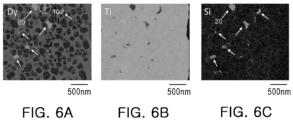
- FIG. 6A is an image obtained by mapping dysprosium (Dy) on a cross-sectional area of 3.0 um ⁇ 3.0 um of the dielectric layer of an example embodiment of the present disclosure using the EDS mode of the scanning transmission electron microscope (STEM)
- FIG. 6B is an image obtained by mapping titanium (Ti) on the same cross-section as that of FIG. 6A using the EDS mode of the scanning transmission electron microscope (STEM)
- FIG. 6C is an image obtained by mapping silicon (Si) on the same cross-section as that of FIG. 6A using the EDS mode of the scanning transmission electron microscope (STEM).
- the high concentration of rare earth elements indicated by a dotted circle (see FIG.
- first, after cutting the first and second directional cross-sections from the third directional center of the body 110, when an image of an arbitrary cross-sectional area of the central portion were captured using a high-angle annular dark field (HAADF) mode of the scanning electron microscopy (SEM), the transmission electron microscopy (TEM), or the scanning transmission electron microscopy (STEM), areas (or grains) observed in white contrast may be primarily interpreted as corresponding to secondary phase grains.
- HAADF high-angle annular dark field
- the first secondary phase grains 10 may correspond to a pyrochlore phase having a cubic crystal system, so that the first secondary phase grains 10 has a shape close to a polygon, and pores may be observed between adjacent barium titanate (BaTiO 3 )-based dielectric grains.
- the second secondary phase grains 20 may have a triclinic crystal system, so that the second secondary phase grains 20 has a grain shape close to amorphous, and may be observed with almost no pores between adjacent barium titanate (BaTiO3)-based dielectric grains.
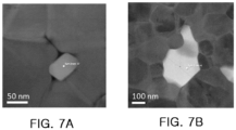
- FIG. 7A is an image of the first secondary phase grain 10 included in the dielectric layer 111 of an example embodiment of the present disclosure captured in the HAADF mode of the scanning transmission electron microscope (STEM)
- FIG. 7B is an image of the second secondary phase grains 20 included in the dielectric layer 111 of an example embodiment of the present disclosure captured in the HAADF mode of the scanning transmission electron microscope (STEM).
- the first secondary phase grain 10 of FIG. 7A has a substantially polygonal shape, and pores are observed between adjacent barium titanate (BaTiO 3 ) dielectric grains
- the second secondary phase grain 20 of FIG. 7b has a shape close to amorphous and no pores are observed between adjacent barium titanate (BaTiO 3 ) dielectric grains.
- the first secondary phase grains 10 may further include barium (Ba), and the average atomic percentage of barium (Ba) included in the first secondary phase grains 10 may be 0.01 at% or more and 6 at% or less.
- first secondary phase grains 10 may further include silicon (Si), and the average atomic percentage of silicon (Si) included in the first secondary phase grains 10 may be 0.05 at% or more and 1.0 at% or less.
- a ratio of the average atomic percentage of the rare earth elements to the average atomic percentage of silicon (Si) included in the second secondary phase grains 20 may be 0.5 or more and 2.0 or less.
- the ratio (RE at%/Si at%) of the average atomic percentage of the rare earth elements (RE at%, where RE is a rare earth element) to the average atomic percentage of silicon (Si at%) included in the second secondary phase grain 20 may be 0.5 or more and 2.0 or less.
- the average atomic percentage of the rare earth elements included in the second secondary phase grains 20 may be 20 at% or more and 25 at% or less, and the average atomic percentage of silicon (Si) included in the second secondary phase grains 20 may be 10 at% or more and 15 at% or less.
- the second secondary phase grains 20 may further include barium (Ba), and the average atomic percentage of barium (Ba) included in the second secondary phase grains 20 may be 1 at% or more and 5 at% or less.
- the second secondary phase grains 20 may further include titanium (Ti), and the average atomic percentage of titanium (Ti) included in the second secondary phase grains 20 may be 0.1 at% or more and 1.0 at% or less.
- the white contrast in FIG. 7A corresponds to the first secondary phase grains 10
- the white contrast in FIG. 7B corresponds to the second secondary phase grains 20.
- dysprosium (Dy), the rare earth element was measured at 10.8 at%
- titanium (Ti) was measured at 16.5 at%
- barium (Ba) was measured at 5.5 at%
- a trace amount of silicon (Si) was measured at 1.0 at% or less
- a ratio of the atomic percentage of dysprosium (Dy), the rare earth element, to the atomic percentage of titanium (Ti) was calculated to be 0.65.
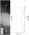
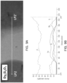
- FIG. 8A is an image of first secondary phase grains 10 included in the dielectric layer of another example embodiment of the present disclosure captured with a scanning transmission electron microscope (STEM), and FIG. 8B is a graph illustrating atomic percentages for each element included in a line-profile after conducting a line-profile (LP1-LP1') to penetrate through the first secondary phase grain 10 of FIG. 8A .
- a region indicated in white contrast in FIG. 8A corresponds to the first secondary phase grains 10, and the other areas indicated in black contrast correspond to barium titanate (BaTiO 3 ) dielectric grains 30.
- BaTiO 3 barium titanate
- the atomic percentage of dysprosium (Dy) was measured to be 20 at% or more and 25 at% or less
- the atomic percentage of titanium (Ti) was measured to be more than 15 at% and 20 at% or less
- the atomic percentage of barium (Ba) was measured to be 0.01 at% or more and 5.5 at% or less
- the atomic percentage of silicon (Si) was measured to be 0.1 at% or more and 0.4 at% or less.
- the atomic percentage of dysprosium (Dy) was measured to be 0.5 at% or more and 2.0 at% or less
- the atomic percentage of titanium (Ti) was measured to be 10 at% or more and 15 at% or less
- the atomic percentage of barium (Ba) was measured to be more than 20 at%
- the atomic percentage of silicon (Si) was measured to be 0.1 at% or more and 0.4 at% or less.
- the atomic percentage of dysprosium (Dy) was measured to be 20 at% or more and 25 at% or less
- the atomic percentage of silicon (Si) was measured to be 10 at% or more and 15 at% or less
- the atomic percentage of barium (Ba) was measured to be 1.5 at% or more and 5.0 at% or less
- the atomic percentage of titanium (Ti) was measured to be 0.5 at% or more and 1.0 at% or less.
- sizes of the first secondary phase grains 10 and the second secondary phase grains 20 serving as a reference are not particularly limited, but the size of the first secondary phase grains 10 may be 50 nm or more and 1 um or less, and the size of the second secondary phase grains 20 may be 100 nm or more and 1 um or less.
- the sizes of the first secondary phase grains 10 and the second secondary phase grains 20 may correspond to values obtained by averaging a major diameter and a minor diameter passing through a center of one secondary phase grain, respectively, but the present disclosure is not limited thereto.
- the capacitance formation portion Ac may satisfy 0 ⁇ A/(A+B) ⁇ 0.4, which may satisfy characteristics in which a room temperature dielectric constant is 1500 or more, characteristics in which a dielectric loss factor (DF) is 1.5% or more, characteristics in which a breakdown voltage (BDV) is 350 V or more, characteristics in which Mean Time to Failure (MTTF) is 200 hours or more under a Highly Accelerated Life Test (HALT) condition applying an electric field of 42 V/ ⁇ m at a temperature of 150 °C, characteristics in which insulation resistance (IR, high temperature insulation resistance) is 3.0E+5 ⁇ or more at a temperature of 150 °C, and X7R characteristic which is a temperature coefficient of capacitance (TCC) according to a target temperature (the capacitance in a temperature range of -55 °C or more and 125 °C or less satisfies -15 % or more and 15% or less based on the capacitance at 25 °C).
- TTCC temperature coefficient of capacitance
- IR high-temperature insulation resistance
- BDV breakdown voltage
- the first and second rare earth elements may be the same, but the present disclosure is not limited thereto, and the first and second rare earth elements may be different from each other, and when each of the first and second rare earth elements includes a plurality of rare earth elements, the first and second rare earth elements may all be the same or only some thereof may be the same, or they may all be different.
- the first and second rare earth elements may be at least one of lanthanum (La), samarium (Sm), dysprosium (Dy), terbium (Tb), holmium (Ho), erbium (Er), and gadolinium (Gd), but may not include at least one of ytterbium (Yb) and yttrium (Y).
- the dielectric layer 111 may include dielectric grains having a core-shell structure including rare earth elements, and in this case, an average atomic percentage of the rare earth elements in the core may be more than 0 at% and less than 0.5 at%, and an average atomic percentage of the rare earth elements in the shell may be 0.5 at% or more and less than 2.0 at%.
- the average atomic percentage of the rare earth elements in the core may satisfy more than 0 at% and less than 0.5 at%, and the average atomic percentage of the rare earth elements in the shell may satisfy 0.5 at% or more and less than 2.0 at%, thereby implementing a highly reliable multilayer electronic component 100.
- the capacitance formation portion Ac may satisfy 0 ⁇ A and 0 ⁇ B, and preferably, the capacitance formation portion Ac may satisfy 0 ⁇ A ⁇ B.
- the capacitance formation portion Ac may include a cross-sectional area of 1.85 um ⁇ 1.85 um satisfying a condition of 0 ⁇ A ⁇ B, and in the cross-sectional area of 1.85 ⁇ m ⁇ 1.85 ⁇ m satisfying the condition of 0 ⁇ A ⁇ B, A and B may satisfy 5 ⁇ A+B ⁇ 20.
- the 1.85 ⁇ m ⁇ 1.85 ⁇ m cross-sectional area of one of the capacitance formation portions Ac may satisfy 0 ⁇ A and 0 ⁇ B, may satisfy 0 ⁇ A ⁇ B, and may satisfy 5 ⁇ A+B ⁇ 20.
- the capacitance formation portion Ac may satisfy 0 ⁇ A and 0 ⁇ B, which may satisfy at least one of characteristics in which a room temperature dielectric constant is 1500 or more, characteristics in which a dielectric loss coefficient (DF) is 1.5% or more, characteristics in which the breakdown voltage (BDV) is 350 V or more, characteristics in which Mean Time to Failure (MTTF) is 200 hours or more under a Highly Accelerated Life Test (HALT) condition applying an electric field of 42 V/ ⁇ m at a temperature of 150 °C, characteristics in which insulation resistance (IR, high temperature insulation resistance) is 3.0E+5 ⁇ or more at a temperature of 150 °C and X7R characteristics which is a temperature coefficient of capacitance (TCC) according to a target temperature.
- DF dielectric loss coefficient
- BDV breakdown voltage
- MTTF Mean Time to Failure
- HALT Highly Accelerated Life Test
- This may provide a highly reliable multilayer electronic component 100 due to the addition of the rare earth elements, but the occurrence of unexpected side effects due to the generation of the first secondary phase grains 10 due to the addition of excessive amounts of rare earth elements may be prevented by generating the second secondary phase grains 20, so that the side effects due to the generation of the first secondary phase grains 10 may be prevented in advance.
- main component may refer to a component that occupies a relatively large weight ratio or atomic number ratio as compared to other components, and refer to 50 wt% or more of a component based on the weight of an entire composition or an entire dielectric layer, or 50 at% or more of a component based on the number of atoms.
- the number of mols of a first subcomponent element compared to 100 mol of a B-site element among the perovskite (ABO 3 )-based main components included in the dielectric layer 111 may be 0.3 mol or more and 0.5 mol or less.
- the main component is barium titanate (BaTiO 3 )
- the number of mols of the first subcomponent element compared to 100 mol of titanium (Ti) included in the dielectric layer 111 may be 0.3 mol or more and 0.5 mol or less.
- the first subcomponent may be added to the dielectric layer 111 in the form of at least one of oxide or carbonate of the first subcomponent element, and as described above, the first subcomponent element may refer to a valence-variable acceptor element.
- a total number of mol of the plurality of first subcomponent elements may be defined as the number of mols of the first subcomponent element.
- the number of mols of the first subcomponent element compared to 100 mol of titanium (Ti) included in the dielectric layer 111 is less than 0.3 mol, there may be a risk in that high-temperature insulation resistance characteristics may deteriorate or the X7R characteristics may not be satisfied, and when the number of mols of the first subcomponent element compared to 100 mol of titanium (Ti) is more than 0.5 mol, there may a risk in that the dielectric constant at room temperature may deteriorate.
- the dielectric layer 111 may further include a second subcomponent element, and the second subcomponent element may be magnesium (Mg).
- the number of mols of the second subcomponent element compared to 100 mol of the B-site element among the perovskite (ABO 3 )-based main components included in the dielectric layer 111 may be 0.3 mol or more and 0.5 mol or less.
- the main component is barium titanate (BaTiO 3 )
- the number of mols of the second subcomponent element compared to 100 mol of titanium (Ti) included in the dielectric layer 111 may be 0.3 mol or more and 0.5 mol or less.
- the second subcomponent may be added to the dielectric layer 111 in the form of at least one of oxide or carbonate of the second subcomponent element, and as described above, the second subcomponent element may refer to magnesium (Mg).
- the number of mols of the second subcomponent element compared to 100 mol of titanium (Ti) included in the dielectric layer 111 is 0.3 mol or more and 0.5 mol or less, excellent high-temperature insulation resistance characteristics may be provided and the X7R characteristics may be satisfied.
- the high-temperature insulation resistance characteristics may deteriorate or the X7R characteristics may not be satisfied, or the breakdown voltage (BDV) characteristics may deteriorate, and when the number of mols of the second subcomponent element compared to 100 mol of titanium (Ti) is more than 0.5 mol, there may be a risk in that the X7R characteristics may not be satisfied.
- the dielectric layer 111 may further include a third subcomponent element, the third subcomponent element may be the rare earth element.
- the rare earth element may preferably be at least one of lanthanum (La), samarium (Sm), dysprosium (Dy), terbium (Tb), holmium (Ho), erbium (Er), and gadolinium (Gd), and may not include at least one of ytterbium (Yb) and yttrium (Y).
- the number of mols of the third subcomponent element compared to 100 mol of the B-site element among the perovskite (ABO 3 )-based main components included in the dielectric layer 111 may be 3.5 mol or more and 5.5 mol or less.
- the main component is barium titanate (BaTiO 3 )
- the number of mols of the third subcomponent element compared to 100 mol of titanium (Ti) included in the dielectric layer 111 may be 3.5 mol or more and 5.5 mol or less.
- the third subcomponent may be added to the dielectric layer 111 in the form of at least one of oxide or carbonate of the third subcomponent element, and as described above, the third subcomponent element may refer to the rare earth element.
- the total number of mol of the plurality of third subcomponent elements may be defined as the number of mols of the third subcomponent element.
- the number of mols of the third subcomponent element compared to 100 mol of titanium (Ti) included in the dielectric layer 111 is 3.5 mol or more and 5.5 mol or less, excellent high-temperature insulation resistance characteristics may be provided the X7R characteristics may be satisfied, breakdown voltage (BDV) characteristics may be provided, and high temperature reliability may be excellent.
- the number of mols of the third subcomponent element compared to 100 mol of titanium (Ti) included in the dielectric layer 111 is less than 3.5 mol, there may be a risk in that the high-temperature insulation resistance characteristics, the breakdown voltage (BDV) characteristics, or the high-temperature reliability may deteriorate, and when the number of mols of the third subcomponent element compared to 100 mol of titanium (Ti) is more than 5.5 mol, there may be a risk in that the room temperature dielectric constant, the loss factor (DF), the high temperature insulation resistance characteristics, or the high temperature reliability may deteriorate.
- BDV breakdown voltage
- the dielectric layer 111 may further include a fourth subcomponent element, and the fourth subcomponent element may be at least one of barium (Ba) and calcium (Ca), and may be, preferably, barium (Ba).
- the number of mols of the fourth subcomponent element compared to 100 mol of the B-site element among the perovskite (ABO 3 )-based main components included in the dielectric layer 111 may be 1 mol or more and 1.5 mol or less.
- the main component is barium titanate (BaTiO 3 )
- the number of mols of the fourth subcomponent element compared to 100 mol of titanium (Ti) included in the dielectric layer 111 may be 1 mol or more and 1.5 mol or less.
- the fourth subcomponent element when the fourth subcomponent element is the same as the A-site element of the main component, the fourth subcomponent element may be calculated excluding the number of mols of the A-site element of the main component.
- the fourth subcomponent is barium (Ba) and the main component is barium titanate (BaTiO 3 )
- the number of mols of barium (Ba) compared to 100 mol of titanium (Ti) included in the dielectric layer 111 may be 101 mol or more and 101.5 mol or less
- the number of mols of barium (Ba) by the fourth subcomponent element may be calculated to be 1 mol or more and 1.5 mol or less, excluding 100 mol of barium (Ba) by the main component.
- the fourth subcomponent may be added to the dielectric layer 111 in the form of at least one of oxide or carbonate of the fourth subcomponent element, and as described above, the fourth subcomponent element may refer to at least one of barium (Ba) and calcium (Ca).
- the total number of mol of the plurality of fourth subcomponent elements may be defined as the number of mols of the fourth subcomponent element.
- the number of mols of the fourth subcomponent element is 1 mol or more and 1.5 mol or less compared to 100 mol of titanium (Ti) included in the dielectric layer 111, excellent high-temperature insulation resistance characteristics may be provided and the X7R characteristics may be satisfied, and the breakdown voltage (BDV) characteristics and the high-temperature reliability may be improved.
- the number of mols of the fourth subcomponent element compared to 100 mol of titanium (Ti) included in the dielectric layer 111 is less than 1 mol, there may be a risk in that the high-temperature insulation resistance properties or the high-temperature reliability may deteriorate, and when the number of mols of the fourth subcomponent element is more than 1.5 mol compared to 100 mol of titanium (Ti), there may be a risk in that the high-temperature insulation resistance characteristics, the breakdown voltage (BDV) characteristics, or the high-temperature reliability may deteriorate.
- BDV breakdown voltage
- the dielectric layer 111 may further include a fifth subcomponent element, and the fifth subcomponent element may be silicon (Si).
- the number of mols of the fifth subcomponent element compared to 100 mol of the B-site element among the perovskite (ABO 3 )-based main components included in the dielectric layer 111 may be 1.1 mol or more and 3 mol or less.
- the main component is barium titanate (BaTiO 3 )
- the number of mols of the fifth subcomponent element compared to 100 mol of titanium (Ti) included in the dielectric layer 111 may be 1.1 mol or more and 3 mol or less.
- the fifth subcomponent may be added to the dielectric layer 111 in the form of at least one of an oxide of the fifth subcomponent element or glass including the fifth subcomponent element, and as described above, the fifth subcomponent element may refer to silicon (Si).
- the number of mols of the fifth subcomponent element compared to 100 mol of titanium (Ti) included in the dielectric layer 111 is 1.1 mol or more and 3 mol or less, excellent high-temperature insulation resistance characteristics may be provided and the X7R characteristics may be satisfied.
- the number of mols of the fifth subcomponent element compared to 100 mol of titanium (Ti) included in the dielectric layer 111 is less than 1.1 mol, the high-temperature insulation resistance characteristics or the high-temperature reliability may deteriorate, and when the number of mols of the fifth subcomponent element compared to 100 mol of titanium (Ti) is more than 3 mol, there may be a risk that the room temperature dielectric constant or the high temperature reliability characteristics may deteriorate.
- a thickness td of the dielectric layer 111 is not limited.
- the thickness of the dielectric layer 111 may be 10.0 um or less. Additionally, in order to achieve miniaturization and high capacity of the multilayer electronic component 100, the thickness of the dielectric layer 111 may be 3.0 ⁇ m or less, and in order to more easily achieve miniaturization and high capacitance, the thickness of the dielectric layer 111 may be 1.0 um or less, preferably 0.6 um or less, and more preferably 0.4 um or less.
- the thickness td of the dielectric layer 111 may refer to a thickness td of the dielectric layer 111 disposed between the first and second internal electrodes 121 and 122.
- the thickness td of the dielectric layer 111 may refer to a first directional size of the dielectric layer 111. Additionally, the thickness td of the dielectric layer 111 may refer to an average thickness td of the dielectric layer 111, and may refer to an average size of the dielectric layer 111 in the first direction.
- the average size of the dielectric layer 111 in the first direction may be measured by scanning images of first and second directional cross-sections of the body 110 with a scanning electron microscope (SEM) of 10,000X magnification. More specifically, the average size of one dielectric layer 111 in the first direction may be an average value calculated by measuring the first directional size of one dielectric layer 111 at 10 points spaced apart from each other at equal intervals in the second direction in the scanned image. The 10 points spaced apart from each other at equal intervals may be designated in the capacitance formation portion Ac. Additionally, when the average value is measured by extending an average value measurement up to 10 dielectric layers 111, an average thickness of the dielectric layers 111 in the first direction may be further generalized
- the internal electrodes 121 and 122 may be alternately stacked with the dielectric layer 111.
- the internal electrodes 121 and 122 may include a first internal electrode 121 and a second internal electrode 122, and the first and second internal electrodes 121 and 122 may be alternately arranged to face each other with the dielectric layer 111 included in the body 110 interposed therebetween, and may be exposed to the third and fourth surfaces 3 and 4 of the body 110, respectively.
- first internal electrode 121 may be spaced apart from the fourth surface 4 and may be exposed through the third surface 3
- second internal electrode 122 may be spaced apart from the third surface 3 and may be exposed through the fourth surface 4.
- a first external electrode 131 may be disposed on the third surface 3 of the body 110 and may be connected to the first internal electrode 121
- a second external electrode 132 may be disposed on the fourth surface 4 of the body 110 and may be connected to the second internal electrode 122.
- first internal electrode 121 may be connected to the first external electrode 131 without being connected to the second external electrode 132
- second internal electrode 122 may be connected to the second external electrode 132 without being connected to the first external electrode 131.
- first and second internal electrodes 121 and 122 may be electrically separated from each other by the dielectric layer 111 disposed therebetween.
- the body 110 may be formed by alternately stacking ceramic green sheets on which the first internal electrode 121 is printed and ceramic green sheets on which the second internal electrode 122 is printed, and then sintering the ceramic green sheets.
- the material included in the internal electrodes 121 and 122 is not particularly limited, and any material having excellent electrical conductivity may be used.
- the internal electrodes 121 and 122 may include one or more of nickel (Ni), copper (Cu), palladium (Pd), silver (Ag), gold (Au), platinum (Pt), tin (Sn), tungsten (W), titanium (Ti), and alloys thereof.
- the internal electrodes 121 and 122 may be formed by printing a conductive paste for internal electrodes including one or more of nickel (Ni), copper (Cu), palladium (Pd), silver (Ag), gold (Au), platinum (Pt), tin (Sn), tungsten (W), titanium (Ti) and alloys thereof on the ceramic green sheet.
- a printing method for the conductive paste for internal electrodes may be a screen printing method or a gravure printing method, but the present disclosure is not limited thereto.
- a thickness te of the internal electrodes 121 and 122 is not limited.
- the thickness te of the internal electrodes 121 and 122 may be 3.0 um or less. Additionally, in order to achieve miniaturization and high capacitance of the multilayer electronic component 100, the thickness of the internal electrodes 121 and 122 may be 1.0 um or less, and in order to more easily achieve ultra-miniaturization and high capacitance, the thickness of the internal electrodes 121 and 122 may be 0.6 um or less, and more preferably 0.4 um or less.
- the average thickness td of at least one of the plurality of dielectric layers 111 and the average thickness te of at least one of the plurality of internal electrodes 121 and 122 may satisfy 2 ⁇ te ⁇ td.
- the average thickness td of one dielectric layer 111 may be larger than twice the average thickness te of one internal electrode 121 or 122.
- the average thickness td of the plurality of dielectric layers 111 may be larger than twice the average thickness te of the plurality of internal electrodes 121 and 122.
- BDV breakdown voltage
- an average thickness of the dielectric layer which is a distance between the internal electrodes, may be thin, which may reduce the breakdown voltage, and a short circuit may occur between the internal electrodes.
- the body 110 may include a first cover portion 112 disposed on one surface of the capacitance formation portion Ac in the first direction, and a second cover portion 113 disposed on the other surface of the capacitance formation portion Ac in the first direction, and more specifically, the body 110 may include an upper cover portion 112 disposed above the capacitance formation portion Ac in the first direction, and a lower cover portion 113 disposed below the capacitance formation portion Ac in the first direction.
- the upper cover portion 112 and the lower cover portion 113 do not include the internal electrodes 121 and 122, and may include the same material as the dielectric layer 111. That is, the upper cover portion 112 and the lower cover portion 113 may include a ceramic material, and may include, for example, a barium titanate (BaTiO 3 )-based ceramic material.
- the thickness tc of the cover portions 112 and 113 is not particularly limited.
- the thickness tc of the cover portions 112 and 113 may be 100 um or less, preferably 30 um or less, and more preferably 20 um or less in ultra-small products.
- the thickness tc of the cover portions 112 and 113 may refer to a first directional size of the cover portions 112 and 113 in the first direction. Additionally, the thickness tc of the cover portions 112 and 113 may refer to the average thickness tc of the cover portions 112 and 113, and may refer to an average size of the cover portions 112 and 113 in the first direction.
- the average size of the cover portions 112 and 113 in the first direction may be measured by scanning images of the first and second directional cross-sections of the body 110 with a scanning electron microscope (SEM) of 10,000X magnification. More specifically, the average size thereof may refer to an average value calculated by measuring the first directional size at 10 points equally spaced from each other in the second direction in the image obtained by scanning one cover portion.
- SEM scanning electron microscope
- the average size of the cover portion in the first direction measured by the above-described method may have substantially the same size as the average size of the cover portion in the first direction in the first and third directional cross-sections of the body 110.
- the multilayer electronic component 100 may include side margin portions 114 and 115 disposed on both end-surfaces of the body 110 in the third direction.
- the side margin portions 114 and 115 may include a first side margin portion 114 disposed on the fifth surface 5 of the body 110 and a second side margin portion 115 disposed on the sixth surface 6 of the body 110.
- the side margin portions 114 and 115 may refer to a region between the end-surfaces of the first and second internal electrodes 121 and 122 in the third direction and a boundary surface of the body 110, based on the first and third directional cross-sections of the body 110.
- the side margin portions 114 and 115 may formed by applying a conductive paste to form the internal electrodes 121 and 122 except where the side margin portions 114 and 115 are to be formed on the ceramic green sheet applied to the capacitance formation portion Ac, and cutting the stacked internal electrodes 121 and 122 so that the internal electrodes 121 and 122 are exposed to the fifth and sixth surfaces 5 and 6 of the body 110 in order to suppress a step portion caused by the internal electrodes 121 and 122, and then stacking a single dielectric layer 111 or two or more dielectric layers 111 on both third directional end-surfaces of the capacitance formation portion Ac in the third direction.
- the side margin portions 114 and 115 may basically serve to prevent damage to the internal electrodes 121 and 122 due to physical or chemical stress.
- the first side margin portion 114 and the second side margin portion 115 do not include the internal electrodes 121 and 122 and may include the same material as the dielectric layer 111. That is, the first side margin portion 114 and the second side margin portion 115 may include a ceramic material, and may include, for example, a barium titanate (BaTiO 3 ) based ceramic material.
- a width wm of the first and second side margin portions 114 and 115 is not particularly limited.
- the width wm of the side margin portions 114 and 115 may be 100 um or less, preferably 30 um or less, and more preferably 20 um or less in ultra-small products.
- the width wm of the side margin portions 114 and 115 may refer to a third directional size of the side margin portions 114 and 115. Additionally, the width wm of the side margin portions 114 and 115 may refer to the average width wm of the side margin portions 114 and 115, and may refer to an average size of the side margin portions 114 and 115 in the third direction.
- the average size of the side margin portions 114 and 115 in the third direction may be measured by scanning images of the first and third directional cross-sections of the body 110 with a scanning electron microscope (SEM) of 10,000X magnification. More specifically, the average size thereof may refer to an average value calculated by measuring the third directional size at 10 points equally spaced apart from each other in the first direction in an image obtained by scanning one side margin portion.
- SEM scanning electron microscope
- the ceramic electronic component 100 has two external electrodes 131 and 132 is described, but the number or shape of the external electrodes 131 and 132 may be changed depending on the shape of the internal electrodes 121 and 122 or other purposes.
- the external electrodes 131 and 132 may be disposed on the body 110 and may be connected to the internal electrodes 121 and 122.
- the external electrodes 131 and 132 may be disposed on the third and fourth surfaces 3 and 4 of the body 110, respectively, and may include first and second external electrodes 131 and 132 connected to the first and second internal electrodes 121 and 122, respectively. That is, the first external electrode 131 may be disposed on the third surface 3 of the body and may be connected to the first internal electrode 121, and the second external electrode 132 may be disposed on the fourth surface 4 of the body and may be connected to the second internal electrode 122.
- the external electrodes 131 and 132 may be disposed to extend to a portion of the first and second surfaces 1 and 2 of the body 110, and may also be disposed to extend to a portion of the fifth and sixth surfaces 5 and 6 of the body 110. That is, the first external electrode 131 may be disposed on a portion of the first, second, fifth, and sixth surfaces 1, 2, 5 and 6 of the body 110 and disposed on the third surface 3 of the body 110, and the second external electrode 132 may disposed on a portion of the first, second, fifth and sixth surfaces 1, 2, 5 and 6 of the body 110 and disposed on the third surface 3 of the body 110.
- the external electrodes 131 and 132 may be formed using any material as long as the material has electrical conductivity, such as a metal, and the specific material may be determined in consideration of electrical properties, structural stability, and the like, and the external electrodes 131 and 132 may further have a multilayer structure.
- the external electrodes 131 and 132 may include an electrode layer disposed on the body 110 and a plating layer disposed on the electrode layer.
- the electrode layer may include first electrode layers 131a and 132a, sintered electrodes including a first conductive metal and glass, or may include second electrode layers 131b and 132b, resin-based electrodes including a second conductive metal and a resin.
- a first conductive metal may refer to a conductive metal included in the first electrode layers 131a and 132a
- a second conductive metal may refer to a conductive metal included in the second electrode layers 131b and 132b.
- the first conductive metal and the second conductive metal may be identical to or different from each other, and when a plurality of conductive metals are included, the same conductive metal may be only partially included, but the present disclosure is not limited thereto.
- the electrode layers 131a, 132a, 131b and 132b may be formed by sequentially forming the sintered electrodes and the resin-based electrodes on the body.
- the electrode layers 131a, 132a, 131b and 132b may be formed by transferring a sheet including a conductive metal onto the body, or may be formed by transferring a sheet including the conductive metal onto the sintered electrode.
- the material having excellent electrical conductivity may be used as conductive metals included in the electrode layers 131a, 132a, 131b and 132b, and for example, the conductive metals may include one or more selected from the group consisting of nickel (Ni), copper (Cu), palladium (Pd), silver (Ag), gold (Au), platinum (Pt), tin (Sn), tungsten (W), titanium (Ti) and alloys thereof, but the present disclosure is not limited thereto.
- the electrode layers 131a, 132a, 131b and 132b may have a bilayer structure including the first electrode layers 131a and 132a and the second electrode layers 131b and 132b, and thus, the external electrodes 131 and 132 may include the first electrode layers 131a and 132a including a first conductive metal and glass, and the second electrode layers 131b and 132b disposed on the first electrode layers 131a and 132a and including a second conductive metal and a resin.
- the first electrode layers 131a and 132a may serve to improve adhesion to the body 110 by including glass, and the second electrode layers 131b and 132b may serve to improve bending strength by including the resin.
- the first conductive metal used in the first electrode layers 131a and 132a is not particularly limited as long as the first conductive metal has a material that may be electrically connected to the internal electrodes 121 and 122 to form electric capacity, and the first conductive metal may include, for example, one or more selected from the group consisting of nickel (Ni), copper (Cu), palladium (Pd), silver (Ag), gold (Au), platinum (Pt), tin (Sn), tungsten (W), titanium (Ti) and alloys thereof.
- the first electrode layers 131a and 132a may be formed by applying a conductive paste prepared by adding glass frit to first conductive metal particles and then sintering the conductive paste.
- the second conductive metal included in the second electrode layers 131b and 132b may serve to electrically connect to the first electrode layers 131a and 132a.
- the second conductive metal included in the second electrode layers 131b and 132b is not particularly limited as long as the second conductive metal has a material that may be electrically connected to the electrode layers 131a and 132a, and the second conductive metal may include one or more selected from the group consisting of nickel (Ni), copper (Cu), palladium (Pd), silver (Ag), gold (Au), platinum (Pt), tin (Sn), tungsten (W), titanium (Ti) and alloys thereof.
- the second conductive metal included in the second electrode layers 131b and 132b may include one or more of spherical particles and flake-shaped particles. That is, the second conductive metal may consist only of flake-shaped particles or only spherical particles, and may be a mixture of flake-shaped particles and spherical particles.
- the spherical particle may include a shape that is not entirely spherical, for example, a shape in which a length ratio of a major axis and a minor axis (major axis/minor axis) is 1.45 or less.
- the flake-shaped particles may refer to particles with a flat and elongated shape, and the present disclosure is not limited thereto, but the length ratio of the major axis and the minor axis (major axis/minor axis) may be, for example, 1.95 or more.
- the lengths of the major and minor axes of the spherical particles and the flake-shaped particles may be measured from images obtained by scanning first and second directional cross-sections cut from the central portion of the multilayer electronic component in the third direction with the scanning electron microscope (SEM).
- the resin included in the second electrode layers 131b and 132b may ensure bonding properties and serve as shock absorbers.
- the resin included in the second electrode layers 131b and 132b may have bonding properties and shock absorption properties, and the resin is not particularly limited as long as the resin may be mixed with the second conductive metal particles to make a paste, and may include, for example, an epoxy-based resin.
- the second electrode layers 131b and 132b may include a plurality of second conductive metal particles, an intermetallic compound, and a resin.
- the intermetallic compound may be included to further improve electrical connectivity with the first electrode layers 131a and 132a.
- the intermetallic compound may serve to improve electrical connectivity by connecting a plurality of metal particles, and may serve to surround the plurality of metal particles and connect the metal particles to each other.
- the intermetallic compound may include a metal having a melting point lower than a curing temperature of the resin. That is, because the intermetallic compound includes the metal having the melting point lower than the curing temperature of the resin, the metal having the melting point lower than the curing temperature of the resin is melted during a drying and curing process, and an intermetallic compound with a portion of the metal particles is formed to surround the metal particle.
- the intermetallic compound may preferably include a low melting point metal of 300 °C or lower.
- the intermetallic compound may include Sn, which has a melting point of 213 to 220 °C. Sn is melted during the drying and curing process, and the melted Sn wets high melting point metal particles such as Ag, Ni or Cu through capillary action, and reacts with some of Ag, Ni or Cu metal particles to form intermetallic compounds such as Ag 3 Sn, Ni 3 Sn 4 , Cu 6 Sn 5 and Cu 3 Sn. Ag, Ni or Cu that did not participate in the reaction remain in the form of metal particles.
- Sn which has a melting point of 213 to 220 °C. Sn is melted during the drying and curing process, and the melted Sn wets high melting point metal particles such as Ag, Ni or Cu through capillary action, and reacts with some of Ag, Ni or Cu metal particles to form intermetallic compounds such as Ag 3 Sn, Ni 3 Sn 4 , Cu 6 Sn 5 and Cu 3 Sn. Ag, Ni or Cu that did not participate in the reaction remain in the form of metal particles.
- the plurality of second conductive metal particles may include one or more of Ag, Ni, and Cu
- the intermetallic compound may include one or more of Ag 3 Sn, Ni 3 Sn 4 , Cu 6 Sn 5 and Cu 3 Sn.
- the plating layers 131c and 132c may serve to improve mounting characteristics.
- plating layers 131c and 132c are not particularly limited, and the plating layers 131c and 132c may be a single layer of plating layers 131c and 132c including one or more of nickel (Ni), tin (Sn), silver (Ag), palladium (Pd) and alloys thereof, or may be formed of a plurality of layers.
- the plating layers 131c and 132c may be Ni plating layers or Sn plating layers, and although not illustrated, the plating layers 131c and 132c may be in the form in which a Ni plating layer and an Sn plating layer are sequentially formed on the electrode layer, and may be in the form in which the Sn plating layer, the Ni plating layer, and the Sn plating layer are formed sequentially. Additionally, the plating layers 131c and 132c may include a plurality of Ni plating layers and/or a plurality of Sn plating layers.
- the thickness of the dielectric layer and internal electrodes must be thinned to increase the number of stacked layers, and thus, the effect according to the present disclosure may be more noticeable in the multilayer electronic component 100 having a size of 3216 (length ⁇ width: 3.2 mm ⁇ 1.6 mm) or less.
- Tables 1, 3 and 5 show RE type of the third subcomponent (where RE represents rare earth elements and the type of added rare earth elements, added in the form of oxides), a sintering temperature, sintering time, sintering atmosphere, and the content of the added first to fifth subcomponent elements.
- the number of mols of the first to fifth subcomponent elements is expressed based on 100 mol of BaTiO 3 , the main component, and all of the first to fifth subcomponent elements correspond to a reference for elements other than oxides.
- the addition of 3.5 mol of the third subcomponent may denote that 3.5 mol of lanthanum (La), a rare earth element, was added as compared to 100 mol of BaTiO 3 , the main component.
- La lanthanum
- Example 6-2 when Mg was decreased to 0.3 mol, it may be seen that the ratio of A/ (A+B) was observed to be 0.17, and the number (A+B) of secondary phase grains was observed to be 6, showing that all characteristics were greater than or equal to the standard value.
- Example 6-3 all characteristics may be seen to be satisfied as in Example 6-2.
- Example 6-4 all characteristics may be seen to be greater than or equal to the standard value except for the TCC at the high temperature of 125 °C.
- Example 6-5 illustrates chip characteristics when Mg was increased by 0.9 mol, and there was no significant change in the ratio of A/(A+B) as in other examples, but it may be seen that the MTTF was increased by 261 hr.
- the content of Dy, the third subcomponent element was changed to 1.5 mol, 2.0 mol, 2.5 mol, 4.5 mol, 5.5 mol, and 6.5 mol, and all other subcomponent contents were the same.
- Example 7-2 illustrates the characteristics when the content of the third subcomponent element is increased by 2.0 mol, from which it may be seen that compared to Example 7-1, the number (A+B) of secondary phase grains in the random observation area (1.85 um ⁇ 1.85 ⁇ m) was increased by 3, and the MTTF was increased from 177 hr to 206 hr. However, it may be seen that the high temperature IR and BDV values fall below the standard values.
- Example 7-3 illustrates the characteristics when the content of the third subcomponent element was increased by 2.5 mol, from which it may be seen that compared to Example 7-2, the number (A+B) of secondary phase grains in the random observation area (1.85 um ⁇ 1.85 ⁇ m) was increased by 4, and the remaining characteristics excluding the BDV was satisfactory.
- the content of the third subcomponent element was increased to 4.5 mol and 5.5 mol, respectively, from which it may be seen that the ratio of A/(A+B) was less than 0.4, which did not significantly affect reliability, and other characteristics also meet the determination standard.
- Example 7-6 illustrates the characteristics in which the content of the third subcomponent element was increased by 6.5 mol, from which it may be seen that the number (A+B) of secondary phase grains in the random observation area (1.85 um ⁇ 1.85 ⁇ m) was increased by 20.
- the ratio of A/(A+B) was also more than or equal to 0.4, from which it may be seen that as the number (A+B) of secondary phase grains increased, A was also increased, and further, it appeared that residual secondary phase grains caused a decrease in high-temperature IR level and rapid deterioration of the MTTF.
- Examples 8-1 to 8-7 illustrate the characteristics in which the content of Ba, the fourth subcomponent element, was changed to 0.25 mol, 0.5 mol, 0.75 mol, 1.25 mol, 1.5 mol, 2.5 mol, and 3.5 mol, and all other subcomponent contents were the same.
- Example 8-1 was an experiment conducted by adding 0.25 mol of the fourth subcomponent element, from which it may be seen that the number (A+B) of secondary phase grains in the random observation area (1.85 um ⁇ 1.85 ⁇ m) was observed to be 15, and the ratio of A/(A+B) was 0.73, thereby generating more first secondary phase grains than second secondary phase grains (A>B).
- Example 8-2 was an experiment conducted by adding 0.5 mol of the fourth subcomponent element, from which it may be seen that the number (A+B) of secondary phase grains in the random observation area (1.85 um ⁇ 1.85 um) was 11, which was reduced compared to Example 8-1. However, the ratio of A/(A+B) ratio was 0.63, which is above 0.4, indicating that more first secondary phase grains were generated than second secondary phase grains (A>B).
- Example 8-3 MLCC was manufactured by adding the fourth subcomponent element by 0.75 mol, from it may be seen that the high-temperature IR level was increased compared to Example 8-2, which meets the specific determination. However, since the ratio of A/(A+B) was 0.5, it may be expected to have bad reliability. It can be seen that the MTTF characteristic of Example 8-3 is 185 hr, which does not meet the determination criteria.
- Example 8-4 and 8-5 the content of the fourth subcomponent element was 1.25 mol and 1.5 mol, respectively, from which it may be seen that all characteristics were met. It may be seen that the number (A+B) of secondary phase grains in the random observation area (1.85 um ⁇ 1.85 ⁇ m) of the two examples was decreased compared to Example 8-3, and fewer first secondary phase grains were generated than second secondary phase grains (A ⁇ B).
- Example 8-6 was an experiment by adding 2.5 mol of the fourth subcomponent element, from which it may be seen that the number (A+B) of secondary phase grains in the random observation area (1.85 um ⁇ 1.85 um) was 3.
- the MTTF characteristics was decreased by 206 hr, and the high-temperature IR and BDV, as well as the TCC at the high-temperature were deteriorated.
- Example 8-7 was an experiment by adding 3.5 mol of the fourth subcomponent element, from which it may be seen that the number (A+B) of secondary phase grains in the random observation area (1.85 um ⁇ 1.85 ⁇ m) was decreased by 2, and only second secondary phase grains exist.
- Example 8-7 it may be seen that the TCC and MTTF at 125 °C and the high temperature IR characteristics did not match. It may be seen that when the content of the fourth subcomponent element is relatively small, the production of first secondary phase grains is promoted, which may cause rapid deterioration of reliability.
- Examples 9-1 to 9-6 was experiments conducted that the content of Si, the fifth subcomponent element, was changed to 0.5 mol, 0.8 mol, 1.1 mol, 1.7 mol, 2.0 mol, and 3.0 mol. The contents of the remaining subcomponent elements are the same.
- Example 9-1 was an experiment conducted by adding 0.5 mol of the fifth subcomponent element, from it may be seen that the number (A+B) of secondary phase grains in the random observation area (1.85 um ⁇ 1.85 ⁇ m) is 16, and more first secondary phase grains were generated (A>B) than second secondary phase grains. This decreased the high temperature IR level by 1.8E+05 ⁇ and decreased the MTTF decreased by 147 hr, which did not meet the characteristic determination.
- Example 9-2 was an embodiment conducted by adding 0.8 mol of the fifth subcomponent element, from it may be seen that the number (A+B) of secondary phase grains in the random observation area (1.85 um ⁇ 1.85 um) was 11 but the ratio of A/(A+B) was 0.55, so that a high temperature IR level reduction and rapid reliability deterioration may be expected due to the high ratio of first secondary phase grains. It may be seen that the high temperature IR level of Example 9-2 was 2.4E+05 ⁇ , and the MTTF was 195 hr, which falls short of the specific determination.
- Example 9-3 was an experiment conducted by adding the content of the fifth subcomponent element at 1.1 mol, from which it may be seen that the number (A + B) of secondary phase grains in the random observation area (1.85 um ⁇ 1.85 ⁇ m) was decreased by 8, and the first secondary phase grains were generated in smaller quantities than the second secondary phase grains. (A ⁇ B), which did not have a significant effect on the IR level or the MTTF value.
- the characteristics of the prototype MLCC chip may be satisfied.
- an example embodiment' used in the present disclosure does not mean the same embodiment, and is provided to emphasize and explain different unique characteristics.
- the embodiments presented above do not preclude being implemented in combination with the features of another embodiment.
- the items described in a specific embodiment are not described in another embodiment, the items may be understood as a description related to another embodiment unless a description opposite or contradictory to the items is in another embodiment.
Landscapes
- Engineering & Computer Science (AREA)
- Power Engineering (AREA)
- Chemical & Material Sciences (AREA)
- Manufacturing & Machinery (AREA)
- Ceramic Engineering (AREA)
- Microelectronics & Electronic Packaging (AREA)
- Inorganic Chemistry (AREA)
- Materials Engineering (AREA)
- Structural Engineering (AREA)
- Organic Chemistry (AREA)
- Fixed Capacitors And Capacitor Manufacturing Machines (AREA)
- Ceramic Capacitors (AREA)
- Thermistors And Varistors (AREA)
- Coils Or Transformers For Communication (AREA)
Applications Claiming Priority (2)
| Application Number | Priority Date | Filing Date | Title |
|---|---|---|---|
| KR20230186897 | 2023-12-20 | ||
| KR1020240019954A KR20250096501A (ko) | 2023-12-20 | 2024-02-08 | 적층형 전자 부품 |
Publications (1)
| Publication Number | Publication Date |
|---|---|
| EP4576141A1 true EP4576141A1 (de) | 2025-06-25 |
Family
ID=93741449
Family Applications (1)
| Application Number | Title | Priority Date | Filing Date |
|---|---|---|---|
| EP24216081.0A Pending EP4576141A1 (de) | 2023-12-20 | 2024-11-28 | Mehrschichtiges elektronisches bauteil |
Country Status (4)
| Country | Link |
|---|---|
| US (1) | US20250210275A1 (de) |
| EP (1) | EP4576141A1 (de) |
| JP (1) | JP2025098965A (de) |
| CN (1) | CN120183900A (de) |
Citations (4)
| Publication number | Priority date | Publication date | Assignee | Title |
|---|---|---|---|---|
| US20140009868A1 (en) * | 2011-03-16 | 2014-01-09 | Murata Manufacturing Co., Ltd | Dielectric ceramic and laminated ceramic capacitor |
| US20190177232A1 (en) * | 2016-06-13 | 2019-06-13 | Corning Incorporated | Aluminum titanate compositions, aluminum titanate articles, and methods of making same |
| US20220130608A1 (en) * | 2020-10-27 | 2022-04-28 | Murata Manufacturing Co., Ltd. | Dielectric ceramic and multilayer ceramic capacitor |
| US20230386745A1 (en) * | 2022-05-30 | 2023-11-30 | Tdk Corporation | Dielectric composition and multilayer ceramic electronic component |
-
2024
- 2024-11-28 EP EP24216081.0A patent/EP4576141A1/de active Pending
- 2024-12-03 US US18/966,932 patent/US20250210275A1/en active Pending
- 2024-12-09 JP JP2024214144A patent/JP2025098965A/ja active Pending
- 2024-12-19 CN CN202411881165.4A patent/CN120183900A/zh active Pending
Patent Citations (4)
| Publication number | Priority date | Publication date | Assignee | Title |
|---|---|---|---|---|
| US20140009868A1 (en) * | 2011-03-16 | 2014-01-09 | Murata Manufacturing Co., Ltd | Dielectric ceramic and laminated ceramic capacitor |
| US20190177232A1 (en) * | 2016-06-13 | 2019-06-13 | Corning Incorporated | Aluminum titanate compositions, aluminum titanate articles, and methods of making same |
| US20220130608A1 (en) * | 2020-10-27 | 2022-04-28 | Murata Manufacturing Co., Ltd. | Dielectric ceramic and multilayer ceramic capacitor |
| US20230386745A1 (en) * | 2022-05-30 | 2023-11-30 | Tdk Corporation | Dielectric composition and multilayer ceramic electronic component |
Also Published As
| Publication number | Publication date |
|---|---|
| JP2025098965A (ja) | 2025-07-02 |
| US20250210275A1 (en) | 2025-06-26 |
| CN120183900A (zh) | 2025-06-20 |
Similar Documents
| Publication | Publication Date | Title |
|---|---|---|
| US9984825B2 (en) | Dielectric ceramic composition, dielectric material, and multilayer ceramic capacitor containing the same | |
| US12482602B2 (en) | Dielectric ceramic composition and multilayer ceramic capacitor comprising the same | |
| US12327685B2 (en) | Multilayer electronic component | |
| JP7813394B2 (ja) | 積層型電子部品及びその製造方法 | |
| US12412704B2 (en) | Multilayer electronic component | |
| EP4576141A1 (de) | Mehrschichtiges elektronisches bauteil | |
| EP4401102A1 (de) | Mehrschichtiger keramikkondensator (mlcc) | |
| US12374500B2 (en) | Multilayer electronic component | |
| EP4557333A1 (de) | Mehrschichtiger keramik kondensator | |
| US12191080B2 (en) | Multilayer ceramic electronic component | |
| EP4421834A2 (de) | Mehrschichtiges elektronisches bauteil | |
| EP4576140A1 (de) | Mehrschichtiges elektronisches bauteil | |
| EP4557337A2 (de) | Mehrschichtiges elektronisches bauelement mit barium, gallium und zinn in den dielektrischen deckschichten | |
| EP4557332A1 (de) | Mehrschichtiger keramischer kondensator | |
| EP4560663A2 (de) | Mehrschichtiges elektronisches bauteil | |
| JP7612965B2 (ja) | 誘電体磁器組成物及びこれを含む積層セラミックキャパシタ | |
| US20250174403A1 (en) | Multilayer electronic component | |
| EP4560665A1 (de) | Mehrschichtiger keramik kondensator | |
| KR20250096501A (ko) | 적층형 전자 부품 |
Legal Events
| Date | Code | Title | Description |
|---|---|---|---|
| PUAI | Public reference made under article 153(3) epc to a published international application that has entered the european phase |
Free format text: ORIGINAL CODE: 0009012 |
|
| STAA | Information on the status of an ep patent application or granted ep patent |
Free format text: STATUS: THE APPLICATION HAS BEEN PUBLISHED |
|
| AK | Designated contracting states |
Kind code of ref document: A1 Designated state(s): AL AT BE BG CH CY CZ DE DK EE ES FI FR GB GR HR HU IE IS IT LI LT LU LV MC ME MK MT NL NO PL PT RO RS SE SI SK SM TR |
|
| STAA | Information on the status of an ep patent application or granted ep patent |
Free format text: STATUS: REQUEST FOR EXAMINATION WAS MADE |
|
| 17P | Request for examination filed |
Effective date: 20251031 |