EP4557896A1 - Method for manufacturing vias in a multi-layered pcb stack - Google Patents
Method for manufacturing vias in a multi-layered pcb stack Download PDFInfo
- Publication number
- EP4557896A1 EP4557896A1 EP23307005.1A EP23307005A EP4557896A1 EP 4557896 A1 EP4557896 A1 EP 4557896A1 EP 23307005 A EP23307005 A EP 23307005A EP 4557896 A1 EP4557896 A1 EP 4557896A1
- Authority
- EP
- European Patent Office
- Prior art keywords
- dielectric layers
- vias
- dielectric
- metallic layer
- pcb stack
- Prior art date
- Legal status (The legal status is an assumption and is not a legal conclusion. Google has not performed a legal analysis and makes no representation as to the accuracy of the status listed.)
- Pending
Links
Images


Classifications
-
- H—ELECTRICITY
- H05—ELECTRIC TECHNIQUES NOT OTHERWISE PROVIDED FOR
- H05K—PRINTED CIRCUITS; CASINGS OR CONSTRUCTIONAL DETAILS OF ELECTRIC APPARATUS; MANUFACTURE OF ASSEMBLAGES OF ELECTRICAL COMPONENTS
- H05K3/00—Apparatus or processes for manufacturing printed circuits
- H05K3/40—Forming printed elements for providing electric connections to or between printed circuits
- H05K3/42—Plated through-holes or plated via connections
- H05K3/421—Blind plated via connections
-
- H—ELECTRICITY
- H05—ELECTRIC TECHNIQUES NOT OTHERWISE PROVIDED FOR
- H05K—PRINTED CIRCUITS; CASINGS OR CONSTRUCTIONAL DETAILS OF ELECTRIC APPARATUS; MANUFACTURE OF ASSEMBLAGES OF ELECTRICAL COMPONENTS
- H05K1/00—Printed circuits
- H05K1/02—Details
- H05K1/11—Printed elements for providing electric connections to or between printed circuits
- H05K1/115—Via connections; Lands around holes or via connections
-
- H—ELECTRICITY
- H05—ELECTRIC TECHNIQUES NOT OTHERWISE PROVIDED FOR
- H05K—PRINTED CIRCUITS; CASINGS OR CONSTRUCTIONAL DETAILS OF ELECTRIC APPARATUS; MANUFACTURE OF ASSEMBLAGES OF ELECTRICAL COMPONENTS
- H05K3/00—Apparatus or processes for manufacturing printed circuits
- H05K3/0011—Working of insulating substrates or insulating layers
- H05K3/0017—Etching of the substrate by chemical or physical means
- H05K3/002—Etching of the substrate by chemical or physical means by liquid chemical etching
-
- H—ELECTRICITY
- H05—ELECTRIC TECHNIQUES NOT OTHERWISE PROVIDED FOR
- H05K—PRINTED CIRCUITS; CASINGS OR CONSTRUCTIONAL DETAILS OF ELECTRIC APPARATUS; MANUFACTURE OF ASSEMBLAGES OF ELECTRICAL COMPONENTS
- H05K1/00—Printed circuits
- H05K1/18—Printed circuits structurally associated with non-printed electric components
- H05K1/181—Printed circuits structurally associated with non-printed electric components associated with surface mounted components
-
- H—ELECTRICITY
- H05—ELECTRIC TECHNIQUES NOT OTHERWISE PROVIDED FOR
- H05K—PRINTED CIRCUITS; CASINGS OR CONSTRUCTIONAL DETAILS OF ELECTRIC APPARATUS; MANUFACTURE OF ASSEMBLAGES OF ELECTRICAL COMPONENTS
- H05K1/00—Printed circuits
- H05K1/18—Printed circuits structurally associated with non-printed electric components
- H05K1/182—Printed circuits structurally associated with non-printed electric components associated with components mounted in printed circuit boards [PCB], e.g. insert-mounted components [IMC]
- H05K1/185—Printed circuits structurally associated with non-printed electric components associated with components mounted in printed circuit boards [PCB], e.g. insert-mounted components [IMC] associated with components encapsulated in the insulating substrate of the PCBs; associated with components incorporated in internal layers of multilayer circuit boards
- H05K1/188—Printed circuits structurally associated with non-printed electric components associated with components mounted in printed circuit boards [PCB], e.g. insert-mounted components [IMC] associated with components encapsulated in the insulating substrate of the PCBs; associated with components incorporated in internal layers of multilayer circuit boards manufactured by mounting on or attaching to a structure having a conductive layer, e.g. a metal foil, such that the terminals of the component are connected to or adjacent to the conductive layer before embedding, and by using the conductive layer, which is patterned after embedding, at least partially for connecting the component
-
- H—ELECTRICITY
- H05—ELECTRIC TECHNIQUES NOT OTHERWISE PROVIDED FOR
- H05K—PRINTED CIRCUITS; CASINGS OR CONSTRUCTIONAL DETAILS OF ELECTRIC APPARATUS; MANUFACTURE OF ASSEMBLAGES OF ELECTRICAL COMPONENTS
- H05K2201/00—Indexing scheme relating to printed circuits covered by H05K1/00
- H05K2201/01—Dielectrics
- H05K2201/0183—Dielectric layers
- H05K2201/0195—Dielectric or adhesive layers comprising a plurality of layers, e.g. in a multilayer structure
-
- H—ELECTRICITY
- H05—ELECTRIC TECHNIQUES NOT OTHERWISE PROVIDED FOR
- H05K—PRINTED CIRCUITS; CASINGS OR CONSTRUCTIONAL DETAILS OF ELECTRIC APPARATUS; MANUFACTURE OF ASSEMBLAGES OF ELECTRICAL COMPONENTS
- H05K2201/00—Indexing scheme relating to printed circuits covered by H05K1/00
- H05K2201/09—Shape and layout
- H05K2201/09209—Shape and layout details of conductors
- H05K2201/095—Conductive through-holes or vias
- H05K2201/09536—Buried plated through-holes, i.e. plated through-holes formed in a core before lamination
-
- H—ELECTRICITY
- H05—ELECTRIC TECHNIQUES NOT OTHERWISE PROVIDED FOR
- H05K—PRINTED CIRCUITS; CASINGS OR CONSTRUCTIONAL DETAILS OF ELECTRIC APPARATUS; MANUFACTURE OF ASSEMBLAGES OF ELECTRICAL COMPONENTS
- H05K2201/00—Indexing scheme relating to printed circuits covered by H05K1/00
- H05K2201/09—Shape and layout
- H05K2201/09209—Shape and layout details of conductors
- H05K2201/095—Conductive through-holes or vias
- H05K2201/09563—Metal filled via
-
- H—ELECTRICITY
- H05—ELECTRIC TECHNIQUES NOT OTHERWISE PROVIDED FOR
- H05K—PRINTED CIRCUITS; CASINGS OR CONSTRUCTIONAL DETAILS OF ELECTRIC APPARATUS; MANUFACTURE OF ASSEMBLAGES OF ELECTRICAL COMPONENTS
- H05K2201/00—Indexing scheme relating to printed circuits covered by H05K1/00
- H05K2201/09—Shape and layout
- H05K2201/09209—Shape and layout details of conductors
- H05K2201/095—Conductive through-holes or vias
- H05K2201/09618—Via fence, i.e. one-dimensional array of vias
-
- H—ELECTRICITY
- H05—ELECTRIC TECHNIQUES NOT OTHERWISE PROVIDED FOR
- H05K—PRINTED CIRCUITS; CASINGS OR CONSTRUCTIONAL DETAILS OF ELECTRIC APPARATUS; MANUFACTURE OF ASSEMBLAGES OF ELECTRICAL COMPONENTS
- H05K2201/00—Indexing scheme relating to printed circuits covered by H05K1/00
- H05K2201/09—Shape and layout
- H05K2201/09209—Shape and layout details of conductors
- H05K2201/095—Conductive through-holes or vias
- H05K2201/09627—Special connections between adjacent vias, not for grounding vias
-
- H—ELECTRICITY
- H05—ELECTRIC TECHNIQUES NOT OTHERWISE PROVIDED FOR
- H05K—PRINTED CIRCUITS; CASINGS OR CONSTRUCTIONAL DETAILS OF ELECTRIC APPARATUS; MANUFACTURE OF ASSEMBLAGES OF ELECTRICAL COMPONENTS
- H05K2203/00—Indexing scheme relating to apparatus or processes for manufacturing printed circuits covered by H05K3/00
- H05K2203/07—Treatments involving liquids, e.g. plating, rinsing
- H05K2203/0703—Plating
- H05K2203/0723—Electroplating, e.g. finish plating
-
- H—ELECTRICITY
- H05—ELECTRIC TECHNIQUES NOT OTHERWISE PROVIDED FOR
- H05K—PRINTED CIRCUITS; CASINGS OR CONSTRUCTIONAL DETAILS OF ELECTRIC APPARATUS; MANUFACTURE OF ASSEMBLAGES OF ELECTRICAL COMPONENTS
- H05K2203/00—Indexing scheme relating to apparatus or processes for manufacturing printed circuits covered by H05K3/00
- H05K2203/07—Treatments involving liquids, e.g. plating, rinsing
- H05K2203/0779—Treatments involving liquids, e.g. plating, rinsing characterised by the specific liquids involved
- H05K2203/0786—Using an aqueous solution, e.g. for cleaning or during drilling of holes
- H05K2203/0789—Aqueous acid solution, e.g. for cleaning or etching
-
- H—ELECTRICITY
- H05—ELECTRIC TECHNIQUES NOT OTHERWISE PROVIDED FOR
- H05K—PRINTED CIRCUITS; CASINGS OR CONSTRUCTIONAL DETAILS OF ELECTRIC APPARATUS; MANUFACTURE OF ASSEMBLAGES OF ELECTRICAL COMPONENTS
- H05K2203/00—Indexing scheme relating to apparatus or processes for manufacturing printed circuits covered by H05K3/00
- H05K2203/10—Using electric, magnetic and electromagnetic fields; Using laser light
- H05K2203/107—Using laser light
-
- H—ELECTRICITY
- H05—ELECTRIC TECHNIQUES NOT OTHERWISE PROVIDED FOR
- H05K—PRINTED CIRCUITS; CASINGS OR CONSTRUCTIONAL DETAILS OF ELECTRIC APPARATUS; MANUFACTURE OF ASSEMBLAGES OF ELECTRICAL COMPONENTS
- H05K2203/00—Indexing scheme relating to apparatus or processes for manufacturing printed circuits covered by H05K3/00
- H05K2203/11—Treatments characterised by their effect, e.g. heating, cooling, roughening
- H05K2203/1184—Underetching, e.g. etching of substrate under conductors or etching of conductor under dielectrics; Means for allowing or controlling underetching
-
- H—ELECTRICITY
- H05—ELECTRIC TECHNIQUES NOT OTHERWISE PROVIDED FOR
- H05K—PRINTED CIRCUITS; CASINGS OR CONSTRUCTIONAL DETAILS OF ELECTRIC APPARATUS; MANUFACTURE OF ASSEMBLAGES OF ELECTRICAL COMPONENTS
- H05K3/00—Apparatus or processes for manufacturing printed circuits
- H05K3/0011—Working of insulating substrates or insulating layers
- H05K3/0017—Etching of the substrate by chemical or physical means
- H05K3/0026—Etching of the substrate by chemical or physical means by laser ablation
- H05K3/0032—Etching of the substrate by chemical or physical means by laser ablation of organic insulating material
- H05K3/0038—Etching of the substrate by chemical or physical means by laser ablation of organic insulating material combined with laser drilling through a metal layer
-
- H—ELECTRICITY
- H05—ELECTRIC TECHNIQUES NOT OTHERWISE PROVIDED FOR
- H05K—PRINTED CIRCUITS; CASINGS OR CONSTRUCTIONAL DETAILS OF ELECTRIC APPARATUS; MANUFACTURE OF ASSEMBLAGES OF ELECTRICAL COMPONENTS
- H05K3/00—Apparatus or processes for manufacturing printed circuits
- H05K3/0011—Working of insulating substrates or insulating layers
- H05K3/0055—After-treatment, e.g. cleaning or desmearing of holes
-
- H—ELECTRICITY
- H05—ELECTRIC TECHNIQUES NOT OTHERWISE PROVIDED FOR
- H05K—PRINTED CIRCUITS; CASINGS OR CONSTRUCTIONAL DETAILS OF ELECTRIC APPARATUS; MANUFACTURE OF ASSEMBLAGES OF ELECTRICAL COMPONENTS
- H05K3/00—Apparatus or processes for manufacturing printed circuits
- H05K3/0094—Filling or covering plated through-holes or blind plated vias, e.g. for masking or for mechanical reinforcement
-
- H—ELECTRICITY
- H05—ELECTRIC TECHNIQUES NOT OTHERWISE PROVIDED FOR
- H05K—PRINTED CIRCUITS; CASINGS OR CONSTRUCTIONAL DETAILS OF ELECTRIC APPARATUS; MANUFACTURE OF ASSEMBLAGES OF ELECTRICAL COMPONENTS
- H05K3/00—Apparatus or processes for manufacturing printed circuits
- H05K3/40—Forming printed elements for providing electric connections to or between printed circuits
- H05K3/42—Plated through-holes or plated via connections
- H05K3/429—Plated through-holes specially for multilayer circuits, e.g. having connections to inner circuit layers
Definitions
- the present disclosure relates to a method for manufacturing vias in a multi-layered PCB stack.
- a classical multi-layer PCB uses vias (holes) to interconnect two or more conductive layers.
- a via is a hole that is mechanically or laser drilled into a dielectric layer and then coated with a conductive metallization (for example copper) in order to electrically and thermally connect at least a top conductive layer and a bottom conductive layer respectively placed above and under the dielectric layer.
- a conductive metallization for example copper
- connections are made with a high density via pattern, in order to have the maximum heat transfer and the lowest electrical resistance.
- One way to improve the thermal performance of the PCB is to increase the via size and/or the density of the vias.
- laser drilling is used to have the smallest via diameter and to cover the connection pad with the maximum number of vias.
- This known technique comprises successive steps of drilling, chemical copper depositing and surface finishing.
- Document US 5,614,114 discloses a detailed drilling path of a laser head which allows obtaining different sizes of the holes with a same precision.
- Document US 4,894,115 discloses a technique to drill a cavity in a polymer material. The laser head follows a specific path in order to create the cavity with a specific shape according to the elements to connect.
- Document EP4095898A1 discloses successive drilling and filling steps allowing increasing the metal density in the PCB, thus improving the thermal resistance. This technique, while offering better thermal performances, increases the manufacturing time, due to multiple successive steps, and the production costs as well.
- Document US 5,764,485 discloses a specific honeycomb or diagonally arranged via pad that allows obtaining a higher current flow capability by increasing the metal density in the PCB board.
- via interconnection is offering locally a good direct thermal path for dispersion of heat, however, the total surface of the top and bottom conductive layers cannot be contacted (this being referred as " discrete interconnection ”) because the number of vias that can be created in a PCB stack il limited by the drilling technology. This limits the overall heat conduction through the PCB stack and results in a higher thermal resistance in comparison with a direct solder of interconnections (" silver sintering " or " metal-based solder ").
- the present disclosure aims at improving the situation.
- the present disclosure aims at addressing at least in part some or all of the limitations of the prior art discussed above, by proposing a solution enabling to increase the metal density between the top and bottom conductive layers, to allow obtaining a better heat extraction from the PCB stack, and to reduce the intrinsic thermal resistance of the via interconnections.
- the present disclosure relates to a method for manufacturing vias in a multi-layered dielectric PCB stack comprising a plurality of alternating first dielectric layers and second dielectric layers, the first dielectric layers comprising a first dielectric material with low glass transition temperature (Tg) and the second dielectric layers comprising a second dielectric material with high glass transition temperature (Tg), a plurality of vias being formed into said plurality of first dielectric layers and second dielectric layers, the method comprising:
- a permanganate desmear process is performed on the multi-layered dielectric PCB stack to at least partially dissolve the first dielectric layers between the vias.
- an electroless metallic deposition is performed on the multi-layered dielectric PCB stack, thus depositing a first metallic layer on internal walls of the plurality of vias, said first metallic layer also filling the spaces between the second dielectric layers left void by the at least partial dissolution of the first dielectric layers, and then a metallic electroplating filling is performed on the multi-layered dielectric PCB stack, thus filling the plurality of vias with a second metallic layer.
- the first metallic layer (68) and the second metallic layer (70) comprise copper.
- the first dielectric layers comprise acrylic and the second dielectric layers comprise FR4.
- obtaining a plurality of vias comprises:
- a bottom metallic layer is placed under the plurality of first dielectric layers and second dielectric layers.
- the top metallic layer comprises copper.
- the bottom metallic layer comprises copper.
- drilling the first dielectric layers and the second dielectric layers comprises mechanically drilling or laser drilling.
- the permanganate desmear process comprises a first sweller step, a second permanganate etching and a third reduction of manganese oxide.
- a multi-layered PCB stack comprising:
- the multi-layered PCB stack further comprises a top metallic layer placed above the plurality of first dielectric layers and second dielectric layers and a bottom metallic layer placed under the plurality of first dielectric layers and second dielectric layers.
- the top metallic layer and the bottom metallic layer of the multi-layered PCB stack comprise copper.
- the present disclosure relates to a method for manufacturing vias in a multi-layered PCB stack that improves the thermal behavior of the via interconnections.
- a via is a hole into a layer of dielectric material forming a PCB stack and isolating two conductive layers, a top and a bottom conductive layer, respectively placed above and below such dielectric material, where the dielectric (epoxy-based) material can be for example acrylic, polyimide or polypropylene based.
- the drilling of the via is always followed by a cleaning chemical bath (called desmear).
- the chemical bath removes the parts of the dielectric material burned, during the drilling step, into the via and/or any remains that are left into the via at the end of the drilling step.
- the chemical bath promotes the adhesion of the metal subsequently deposited in the via by increasing the conductive layer rugosity, as detailed here below, because it cleans the internal walls of the via.
- the cleaning chemical bath is usually a permanganate-based bath which uses oxidation chemical reaction to roughen the edge of the via.
- Figure 1(a) - 1(c) show three different ways of drilling a PCB stack.
- a UV laser process is shown
- a CO 2 laser process is shown
- an eximer laser process is shown.
- FIG. 1(a) shows an initial phase 100a wherein a PCB stack 1 is created, the PCB stack 1, shown in sectional view, including a dielectric layer 2 placed on a substrate 4 with a bottom conductive layer 6 placed in-between and a RCC (resin-coated-copper) layer 8 placed above the dielectric layer 2.
- the RCC layer 8 is etched with an UV laser and an opening 10 is created.
- an UV laser ablation is performed, thus etching the dielectric layer 2 to create a hole (via) 12.
- phase 106a desmear and metallization processes are performed, and further a mask 14 is deposited on top of the PCB stack 1.
- phase 108a a metallic deposition is performed, to cover the PCB stack 1 and the hole 12 with a metallic layer 16 and finally, in phase 110a, a final etching is performed to remove the mask 14 and the portion of the RCC layer 8 that was under the mask 14.
- Figure 1(b) shows an initial phase 100b corresponding to the phase 100a previously disclosed.
- a chemical copper reduction is performed and the opening 10 is created.
- a CO 2 laser ablation is performed, thus obtaining the hole 12.
- Phases 106b, 108b and 110b correspond to phases 106a, 108a and 110a above disclosed.
- Figure 1(c) shows an initial phase 100c wherein a dielectric substrate (layer) 20 is provided.
- phase 102c a UV laser ablation is performed, thus etching a hole (via) 22.
- phase 104c a desmear and metallization processes are performed, and a metallic layer 24 in the hole 22 and on top of the substrate 20 is deposited.
- phase 106c an eximer laser process is performed and then a mask 26 is deposited above and below the substrate 20.
- a metallic deposition is performed, to cover the substrate 20 and the hole 22 with a metallic layer 28.
- phase 110c a final etching is performed to remove the mask 26.
- the permanganate used in the desmear processes above disclosed shows a faster attack on materials with low Tg (glass transition temperature), i.e., with temperature values below 100°C, such as for example acrylic, thus resulting in a deep etching of the material.
- Tg glass transition temperature
- the speed of dissolution is function of the dielectric material.
- materials having different values of Tg are used to create the PCB stack, so that it is possible to get controlled vias (cavities) during the desmear process and then to fill such cavities with a metal (e.g., copper) through a metal deposition process.
- a metal e.g., copper
- the resulting multi-layered PCB stack contains higher density of metal, thus leading to better thermal performances.
- the desmear is a key process to perform prior to the metal deposition (metal plating) to ensure proper adhesion of the metal to the internal walls of the via. Wet treatments are applied during a desmear process.
- Permanganate etching presents the advantages of being more environmentally friendly than chromic acid etching and being readily applicable to a wide class of polymers and composites.
- the permanganate desmear process (sequence) consists of three steps: a first sweller step, a second permanganate etching and a third reduction of manganese oxide.
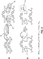
- Figures 2(a) - 2(c) show the chemical reactions that take place during the three steps of the permanganate desmear sequence.
- the permanganate ions preferentially attack the polymer chains in the previously formed clusters because of electrostatic interactions. Indeed, it has been determined that the permanganate ions attack both carbons in ⁇ -position of the alcohol and ether groups, the inductive effect from the oxygen leading to a weakening of the vicinal carbon-carbon bonds.
- the conditions of oxidation are strong, leading to an alteration of the burned epoxy, by weakening the vicinal carbon-carbon bonds and removing few micrometers of thickness from the surface in the case of epoxy.
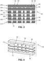
- Figure 3 shows the steps of a method for manufacturing vias in a multi-layered PCB stack according to the present invention.
- a multi-layered dielectric PCB stack 50 i.e., a PCB stack comprising a plurality of alternating first dielectric layers 52 and second dielectric layers 54, is provided in a first step 200 and it is shown in sectional view on top of Figure 3 .
- the first dielectric layers 52 comprise a first dielectric material with low Tg such as acrylic and the second dielectric layers 54 comprise a second dielectric material with high Tg such as FR4.
- the expression “low Tg” refers to glass transition temperatures below or equal to a threshold value of 100°C.
- the expression “high Tg” refers to glass transition temperatures higher than such threshold value of 100°C.
- the multi-layered PCB stack 50 further comprises a top metallic layer 56 and a bottom metallic layer 58, preferably made of copper, placed above and under the stack of first dielectric layers 52 and second dielectric layers 54 (referred in the following as dielectric stack), respectively.
- the top metallic layer 56 is etched according to a predetermined pattern, thus leaving a plurality of masking areas 60 covering the dielectric stack placed underneath and leaving corresponding uncovered areas 62 where the dielectric stack is not covered by the top metallic layer 56.
- step 204 the dielectric stack is mechanically or laser drilled in correspondence of the uncovered areas 62, thus obtaining a plurality of vias (holes) 64.
- a permanganate desmear process (i.e., the sequence comprising the three baths above-disclosed) is performed on the multi-layered PCB stack 50 and then, in step 208, an electroless metallic deposition is performed on the multi-layered PCB stack 50, thus depositing a first metallic layer 68, preferably copper, on the internal walls of the plurality of vias 64.
- the first dielectric layers 52 at least partially (part of the first dielectric layers 52) dissolve and when the electroless metallic deposition 208 is performed, the first metallic layer 68 also fills the spaces between the second dielectric layers 54 left void by the at least partial dissolution of the first dielectric layers 52.
- the first dielectric layers 52 completely dissolve.
- step 210 a metallic electroplating filling is performed on the multi-layered PCB stack 50, thus filling the plurality of vias 64 with a second metallic layer 70, preferably copper.
- the vias 64 become interconnected each other through a metallic network 72 (see Figure 4 ) made up by the first metal layer 68 replacing the dissolved first dielectric layers 52.
- the multi-layered PCB stack 50 comprises therefore a sandwich of materials having different Tg (the first and second dielectric layers 52, 54) in order to get different etching speeds during the desmear process. This results in the erosion of the first dielectric layers 52 during the desmear process, then, the vias 64 and the spaces between the second dielectric layers 54 are filled with a metal during the electroless deposition step 208 and electroplating filling step 210.
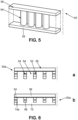
- Figure 4 shows a tridimensional view of the multi-layered PCB stack 50 including the metallic network 72 above disclosed while Figure 5 shows a tridimensional view of a PCB stack 50' of the prior art which does not comprise such metallic network 72.
- Figure 5 some references corresponding to the ones of Figure 4 have been reported.
- the first metallic layer 68 filling the spaces between the second dielectric layers 54 and previously occupied by the first dielectric layers 52 results in the metallic network 52 interconnecting the plurality of vias 64 and being placed between the top metallic layer 56 and the bottom metallic layer 58.
- Table 1 lists different dielectric materials that can be used for the first dielectric layers 52 and the second dielectric layers 54, together with their respective Tg value.
- materials having a greater difference between their respective Tg values should be selected as material for the first and second dielectric layers 52, 54, respectively, in order to have the material of the fist dielectric layers 52 (the one with the lower Tg value) dissolved much more than the material of the second dielectric layers 54 (the one with the higher Tg value).
- Figure 6(a) shows a sectional view of a first multi-layered PCB stack sample 50a in a first configuration before the desmear process is applied in step 206, wherein in such first configuration only a first dielectric layer 52 is present.
- Figure 6(b) shows the first multi-layered PCB stack sample 50a of Figure 6(a) the end of the metallic electroplating filling step 210, wherein the first metallic layer 68 and the second metallic layer 70 have filled the space cleaned from the first dielectric layer 52 during the desmear process.
- Figure 7(a) shows a sectional view of a second multi-layered PCB stack sample 50b in a second configuration before the desmear process is applied in step 206, wherein in such second configuration three first dielectric layers 52 are present.
- Figure 7(b) shows the second multi-layered PCB stack sample 50b of Figure 7(a) the end of the metallic electroplating filling step 210, wherein the first metallic layer 68 and the second metallic layer 70 have filled the spaces cleaned from the first dielectric layer 52 during the desmear process.
- Figure 8 shows a sectional view of a reference PCB stack sample 50c at the end of the metallic electroplating filling step 210.
- the reference stack 50c includes a top conductive layer 56' and vias 64' made up of a single dielectric material.
- the vias 64 interconnecting the multi-layered PCB stack samples 50a, 50b to an external layer are also interconnected each other by a single fin 74a or three fins 74b.
- the thicknesses of the materials in the first and second multi-layered PCB stack samples 50a, 50b have been selected following available materials specifications, in particular FR4 from Panasonic R1766 has been taken for the second dielectric layers 54 (having Tg of 150°C) and an acrylic layer from Dupont LF100 has been taken for the first dielectric layers 52 (having Tg of 45°C).
- Table 2 shows the junction to ambient thermal resistance (RthJA) values of the reference PCB stack sample 50c and of the multi-layered PCB stack samples 50a, 50b in the two configurations, where the maximum and minimum junction temperatures, located within the embedded die and at the bottom side of the package are indicated.
- Rth benefit column is indicated the percentage of improvement of the junction to ambient thermal resistance value of the multi-layered PCB stack samples 50a, 50b with respect to the reference PCB stack sample 50c.
- the results of the FEM simulations indicate a clear improvement of the RthJA value when applied on a single side of the embedded die (25% for three fins). This improvement could be increased by applying this technique to both sides of a die. Moreover, by increasing the density of metal through a higher number of fins, the heat extraction and thus the RthJA further improve.
- the method according to the present inventions has also the advantage of allowing manufacturing a multi-layered PCB stack by performing standard process steps because it does not modify the fabricating technique of the PCB stack itself.
- the improvement of the thermal behavior of the via interconnections is due to the selection of the materials to be used to fabricate the multi-layered dielectric stack, to get the corrosion of the first dielectric layers 52 during the desmear process and further fill with the metal.
Landscapes
- Engineering & Computer Science (AREA)
- Microelectronics & Electronic Packaging (AREA)
- Manufacturing & Machinery (AREA)
- Chemical & Material Sciences (AREA)
- Chemical Kinetics & Catalysis (AREA)
- General Chemical & Material Sciences (AREA)
- Production Of Multi-Layered Print Wiring Board (AREA)
Abstract
A method for manufacturing vias in a multi-layered dielectric PCB stack (50) comprising a plurality of alternating first dielectric layers (52) and second dielectric layers (54), the first dielectric layers (52) comprising a first dielectric material with low glass transition temperature (Tg) and the second dielectric layers (54) comprising a second dielectric material with high glass transition temperature (Tg), a plurality of vias (64) being formed (202, 204) into said plurality of first dielectric layers (52) and second dielectric layers (54),
the method comprising:
- at least partially dissolving (206) the first dielectric layers (52) between the vias (64);
- filling (208, 210) with metal (68, 70) the vias (64) and the spaces between the second dielectric layers (54) left void by the at least partial dissolution of the first dielectric layers (52), thus obtaining a metallic network (72) interconnecting the vias (64) each other.
the method comprising:
- at least partially dissolving (206) the first dielectric layers (52) between the vias (64);
- filling (208, 210) with metal (68, 70) the vias (64) and the spaces between the second dielectric layers (54) left void by the at least partial dissolution of the first dielectric layers (52), thus obtaining a metallic network (72) interconnecting the vias (64) each other.
Description
- The present disclosure relates to a method for manufacturing vias in a multi-layered PCB stack.
- A classical multi-layer PCB (printed circuit board) uses vias (holes) to interconnect two or more conductive layers. A via is a hole that is mechanically or laser drilled into a dielectric layer and then coated with a conductive metallization (for example copper) in order to electrically and thermally connect at least a top conductive layer and a bottom conductive layer respectively placed above and under the dielectric layer.
- In the case of a PCB embedded power die, connections are made with a high density via pattern, in order to have the maximum heat transfer and the lowest electrical resistance.
- In fact, in a PCB the heat follows the conductive paths due to better thermal conductivity than in the dielectric layer.
- One way to improve the thermal performance of the PCB is to increase the via size and/or the density of the vias. To do so, laser drilling is used to have the smallest via diameter and to cover the connection pad with the maximum number of vias. This known technique comprises successive steps of drilling, chemical copper depositing and surface finishing.
- Different techniques of drilling are known which allow getting different size, shape and depth of the vias, with more or less speed and/or precision in the realization of the vias. Document
US 5,614,114 discloses a detailed drilling path of a laser head which allows obtaining different sizes of the holes with a same precision. DocumentUS 4,894,115 discloses a technique to drill a cavity in a polymer material. The laser head follows a specific path in order to create the cavity with a specific shape according to the elements to connect. DocumentEP4095898A1 discloses successive drilling and filling steps allowing increasing the metal density in the PCB, thus improving the thermal resistance. This technique, while offering better thermal performances, increases the manufacturing time, due to multiple successive steps, and the production costs as well. DocumentUS 5,764,485 discloses a specific honeycomb or diagonally arranged via pad that allows obtaining a higher current flow capability by increasing the metal density in the PCB board. - All the above-mentioned solutions suffer from a thermal limitation of the via interconnections. In fact, via interconnection is offering locally a good direct thermal path for dispersion of heat, however, the total surface of the top and bottom conductive layers cannot be contacted (this being referred as "discrete interconnection") because the number of vias that can be created in a PCB stack il limited by the drilling technology. This limits the overall heat conduction through the PCB stack and results in a higher thermal resistance in comparison with a direct solder of interconnections ("silver sintering" or "metal-based solder").
- The present disclosure aims at improving the situation. In particular, the present disclosure aims at addressing at least in part some or all of the limitations of the prior art discussed above, by proposing a solution enabling to increase the metal density between the top and bottom conductive layers, to allow obtaining a better heat extraction from the PCB stack, and to reduce the intrinsic thermal resistance of the via interconnections.
- For this purpose, the present disclosure relates to a method for manufacturing vias in a multi-layered dielectric PCB stack comprising a plurality of alternating first dielectric layers and second dielectric layers, the first dielectric layers comprising a first dielectric material with low glass transition temperature (Tg) and the second dielectric layers comprising a second dielectric material with high glass transition temperature (Tg), a plurality of vias being formed into said plurality of first dielectric layers and second dielectric layers, the method comprising:
- at least partially dissolving the first dielectric layers between the vias;
- filling with metal the vias and the spaces between the second dielectric layers left void by the at least partial dissolution of the first dielectric layers, thus obtaining a metallic network interconnecting the vias each other.
- In an embodiment, a permanganate desmear process is performed on the multi-layered dielectric PCB stack to at least partially dissolve the first dielectric layers between the vias.
- In an embodiment, to fill the vias with metal an electroless metallic deposition is performed on the multi-layered dielectric PCB stack, thus depositing a first metallic layer on internal walls of the plurality of vias, said first metallic layer also filling the spaces between the second dielectric layers left void by the at least partial dissolution of the first dielectric layers, and then a metallic electroplating filling is performed on the multi-layered dielectric PCB stack, thus filling the plurality of vias with a second metallic layer.
- In an embodiment, the first metallic layer (68) and the second metallic layer (70) comprise copper.
- In an embodiment, the first dielectric layers comprise acrylic and the second dielectric layers comprise FR4.
- In an embodiment, obtaining a plurality of vias comprises:
- placing a top metallic layer above the plurality of first dielectric layers and second dielectric layers;
- etching the top metallic layer according to a predetermined pattern, thus leaving a plurality of masking areas covering the first dielectric layers and the second dielectric layers placed underneath and leaving corresponding uncovered areas where the first dielectric layers and the second dielectric layers are not covered by the top metallic layer;
- drilling the first dielectric layers and the second dielectric layers in correspondence of the uncovered areas, thus obtaining the plurality of vias.
- In an embodiment, a bottom metallic layer is placed under the plurality of first dielectric layers and second dielectric layers.
- In an embodiment, the top metallic layer comprises copper.
- In an embodiment, the bottom metallic layer comprises copper.
- In an embodiment, drilling the first dielectric layers and the second dielectric layers comprises mechanically drilling or laser drilling.
- In an embodiment, the permanganate desmear process comprises a first sweller step, a second permanganate etching and a third reduction of manganese oxide.
- Also provided herein is a multi-layered PCB stack comprising:
- a plurality of alternating first dielectric layers and second dielectric layers, the first dielectric layers comprising a first dielectric material with low glass transition temperature (Tg) and the second dielectric layers comprising a second dielectric material with high glass transition temperature (Tg);
- a plurality of vias drilled into said plurality of first dielectric layers and second dielectric layers, the first dielectric layers being at least partially dissolved between the vias, wherein the vias and the spaces between the second dielectric layers left void by the at least partial dissolution of the first dielectric layers are filled with metal, thus obtaining a metallic network interconnecting the vias each other.
- In an embodiment, the multi-layered PCB stack further comprises a top metallic layer placed above the plurality of first dielectric layers and second dielectric layers and a bottom metallic layer placed under the plurality of first dielectric layers and second dielectric layers.
- In an embodiment, the top metallic layer and the bottom metallic layer of the multi-layered PCB stack comprise copper.
- Further characteristics and advantages of the present invention will become apparent from the following description, provided merely by way of a non-limiting example, with reference to the attached drawings, in which:
-
Figures 1(a) - 1(c) show three different ways of drilling a PCB stack; -
Figures 2(a) - 2(c) show the chemical reactions that take place during the three steps of the permanganate desmear sequence; - Figure shows the steps of a method for manufacturing vias in a multi-layered PCB stack according to the present invention;
-
Figure 4 shows a tridimensional view of a multi-layered PCB stack including a metallic network; -
Figure 5 shows a tridimensional view of a PCB stack which does not comprise the metallic network; -
Figure 6(a) shows a sectional view of a first multi-layered PCB stack sample in a first configuration before the desmear process is applied; -
Figure 6(b) shows the first sample ofFigure 6(a) the end of the metallic electroplating filling step; -
Figure 7(a) shows a sectional view of a second multi-layered PCB stack sample in a second configuration before the desmear process is applied; -
Figure 7(b) shows the second sample ofFigure 7(a) the end of the metallicelectroplating filling step 210, and -
Figure 8 shows a sectional view of a reference stack at the end of the metallic electroplating filling step. - The present disclosure relates to a method for manufacturing vias in a multi-layered PCB stack that improves the thermal behavior of the via interconnections.
- A via is a hole into a layer of dielectric material forming a PCB stack and isolating two conductive layers, a top and a bottom conductive layer, respectively placed above and below such dielectric material, where the dielectric (epoxy-based) material can be for example acrylic, polyimide or polypropylene based.
- The drilling of the via, performed mechanically or by laser, is always followed by a cleaning chemical bath (called desmear). The chemical bath removes the parts of the dielectric material burned, during the drilling step, into the via and/or any remains that are left into the via at the end of the drilling step. Moreover, the chemical bath promotes the adhesion of the metal subsequently deposited in the via by increasing the conductive layer rugosity, as detailed here below, because it cleans the internal walls of the via. The cleaning chemical bath is usually a permanganate-based bath which uses oxidation chemical reaction to roughen the edge of the via.
-
Figure 1(a) - 1(c) show three different ways of drilling a PCB stack. In particular, inFigure 1(a) a UV laser process is shown, inFigure 1(b) a CO2 laser process is shown and inFigure 1(c) an eximer laser process is shown. -
Figure 1(a) shows aninitial phase 100a wherein aPCB stack 1 is created, thePCB stack 1, shown in sectional view, including adielectric layer 2 placed on asubstrate 4 with a bottomconductive layer 6 placed in-between and a RCC (resin-coated-copper)layer 8 placed above thedielectric layer 2. In anext phase 102a, theRCC layer 8 is etched with an UV laser and anopening 10 is created. Inphase 104a, an UV laser ablation is performed, thus etching thedielectric layer 2 to create a hole (via) 12. Then, inphase 106a, a desmear and metallization processes are performed, and further amask 14 is deposited on top of thePCB stack 1. Then, inphase 108a, a metallic deposition is performed, to cover thePCB stack 1 and thehole 12 with ametallic layer 16 and finally, inphase 110a, a final etching is performed to remove themask 14 and the portion of theRCC layer 8 that was under themask 14. -
Figure 1(b) shows aninitial phase 100b corresponding to thephase 100a previously disclosed. In anext phase 102b, a chemical copper reduction is performed and theopening 10 is created. Inphase 104b, a CO2 laser ablation is performed, thus obtaining thehole 12.Phases phases -
Figure 1(c) shows aninitial phase 100c wherein a dielectric substrate (layer) 20 is provided. Inphase 102c a UV laser ablation is performed, thus etching a hole (via) 22. Inphase 104c, a desmear and metallization processes are performed, and ametallic layer 24 in thehole 22 and on top of thesubstrate 20 is deposited. In anext phase 106c an eximer laser process is performed and then amask 26 is deposited above and below thesubstrate 20. In aphase 108c, a metallic deposition is performed, to cover thesubstrate 20 and thehole 22 with ametallic layer 28. Finally, inphase 110c, a final etching is performed to remove themask 26. - The permanganate used in the desmear processes above disclosed shows a faster attack on materials with low Tg (glass transition temperature), i.e., with temperature values below 100°C, such as for example acrylic, thus resulting in a deep etching of the material. The speed of dissolution is function of the dielectric material.
- Therefore, according to the method for manufacturing vias in a multi-layered PCB stack of the present invention, further disclosed in detail, materials having different values of Tg are used to create the PCB stack, so that it is possible to get controlled vias (cavities) during the desmear process and then to fill such cavities with a metal (e.g., copper) through a metal deposition process.
- Therefore, the resulting multi-layered PCB stack contains higher density of metal, thus leading to better thermal performances.
- The desmear is a key process to perform prior to the metal deposition (metal plating) to ensure proper adhesion of the metal to the internal walls of the via. Wet treatments are applied during a desmear process.
- Among the wet-treatments, alkaline permanganate etching was developed during the 1980's, it is efficient and cheap, and continues to be the most widely used desmear process. Permanganate etching presents the advantages of being more environmentally friendly than chromic acid etching and being readily applicable to a wide class of polymers and composites.
- The permanganate desmear process (sequence) consists of three steps: a first sweller step, a second permanganate etching and a third reduction of manganese oxide.
-
Figures 2(a) - 2(c) show the chemical reactions that take place during the three steps of the permanganate desmear sequence. - In particular in
Figure 2(a) sweller molecules 30 diffuse through an epoxy polymer network, inFigure 2(b) permanganate ions MnO4 2- attack the polymers from the surface leading to cavities at the polymer surface (see dotted line 32) and in the equation ofFigure 2(c) the MnOz is reactively dissolved by reduction with hydroxylammonium (or peroxide) yielding aqueous manganese ions and gaseous nitrogen (or water). - During the oxidative etching bath, the permanganate ions preferentially attack the polymer chains in the previously formed clusters because of electrostatic interactions. Indeed, it has been determined that the permanganate ions attack both carbons in α-position of the alcohol and ether groups, the inductive effect from the oxygen leading to a weakening of the vicinal carbon-carbon bonds. The conditions of oxidation are strong, leading to an alteration of the burned epoxy, by weakening the vicinal carbon-carbon bonds and removing few micrometers of thickness from the surface in the case of epoxy.
-
Figure 3 shows the steps of a method for manufacturing vias in a multi-layered PCB stack according to the present invention. - A multi-layered
dielectric PCB stack 50, i.e., a PCB stack comprising a plurality of alternating firstdielectric layers 52 and second dielectric layers 54, is provided in afirst step 200 and it is shown in sectional view on top ofFigure 3 . - Advantageously, the first dielectric layers 52 comprise a first dielectric material with low Tg such as acrylic and the second dielectric layers 54 comprise a second dielectric material with high Tg such as FR4. In the present description, the expression "low Tg" refers to glass transition temperatures below or equal to a threshold value of 100°C. Similarly, the expression "high Tg" refers to glass transition temperatures higher than such threshold value of 100°C.The
multi-layered PCB stack 50 further comprises a topmetallic layer 56 and a bottommetallic layer 58, preferably made of copper, placed above and under the stack of firstdielectric layers 52 and second dielectric layers 54 (referred in the following as dielectric stack), respectively. - In a
second step 202, the topmetallic layer 56 is etched according to a predetermined pattern, thus leaving a plurality of maskingareas 60 covering the dielectric stack placed underneath and leaving corresponding uncoveredareas 62 where the dielectric stack is not covered by the topmetallic layer 56. - Then, in
step 204, the dielectric stack is mechanically or laser drilled in correspondence of the uncoveredareas 62, thus obtaining a plurality of vias (holes) 64. - In a
further step 206, a permanganate desmear process (i.e., the sequence comprising the three baths above-disclosed) is performed on themulti-layered PCB stack 50 and then, instep 208, an electroless metallic deposition is performed on themulti-layered PCB stack 50, thus depositing a firstmetallic layer 68, preferably copper, on the internal walls of the plurality ofvias 64. - During the permanganate desmear process the first dielectric layers 52 at least partially (part of the first dielectric layers 52) dissolve and when the electroless
metallic deposition 208 is performed, the firstmetallic layer 68 also fills the spaces between the second dielectric layers 54 left void by the at least partial dissolution of the first dielectric layers 52. - Alternatively, the first dielectric layers 52 completely dissolve.
- As a result, metallic rings around the
vias 64, at least partially penetrating into the dielectric stack in correspondence of the fist dielectric layers 52, are formed. - Finally, in
step 210, a metallic electroplating filling is performed on themulti-layered PCB stack 50, thus filling the plurality ofvias 64 with a secondmetallic layer 70, preferably copper. - Thanks to the alternance, in the
multi-layered PCB stack 50, of firstdielectric layers 52 and second dielectric layers 54 with different Tg, thevias 64 become interconnected each other through a metallic network 72 (seeFigure 4 ) made up by thefirst metal layer 68 replacing the dissolved first dielectric layers 52. - The
multi-layered PCB stack 50 comprises therefore a sandwich of materials having different Tg (the first and second dielectric layers 52, 54) in order to get different etching speeds during the desmear process. This results in the erosion of the first dielectric layers 52 during the desmear process, then, thevias 64 and the spaces between the second dielectric layers 54 are filled with a metal during theelectroless deposition step 208 andelectroplating filling step 210. -
Figure 4 shows a tridimensional view of themulti-layered PCB stack 50 including themetallic network 72 above disclosed whileFigure 5 shows a tridimensional view of a PCB stack 50' of the prior art which does not comprise suchmetallic network 72. InFigure 5 some references corresponding to the ones ofFigure 4 have been reported. - As shown in
Figure 4 , in comparison with the PCB stack 50' ofFigure 5 , the firstmetallic layer 68 filling the spaces between the second dielectric layers 54 and previously occupied by the first dielectric layers 52 results in themetallic network 52 interconnecting the plurality ofvias 64 and being placed between the topmetallic layer 56 and the bottommetallic layer 58. - Table 1 lists different dielectric materials that can be used for the first dielectric layers 52 and the second dielectric layers 54, together with their respective Tg value.
- In order to get the best performances during the desmear process, materials having a greater difference between their respective Tg values should be selected as material for the first and second dielectric layers 52, 54, respectively, in order to have the material of the fist dielectric layers 52 (the one with the lower Tg value) dissolved much more than the material of the second dielectric layers 54 (the one with the higher Tg value).
Table 1 Material Tg [°C] Polyimide 250 Polyimide 260 PPO 250 PPO 250 PPO 250 PTFE 326 FR4 140 FR5 180 Acrylic 45 Bisphenol A 100 - In the context of PCB embedded power dies, increasing the density of the metal on the top and/or bottom side of the die helps achieving higher overall heat transfer coefficient of the package, and reducing the junction to ambient thermal resistance (RthJA).
- FEM analyses have been carried out for multi-layered PCB stack samples (corresponding to the
multi-layered PCB stack 50 above-disclosed) and have been compared to a reference PCB stack sample wherein only one material is used as dielectric layer (corresponding to PCB stack 50' above-shown). -
Figure 6(a) shows a sectional view of a first multi-layeredPCB stack sample 50a in a first configuration before the desmear process is applied instep 206, wherein in such first configuration only afirst dielectric layer 52 is present. - Elements corresponding to the ones of the
multi-layered PCB stack 50 above-disclosed are indicated with the same references. -
Figure 6(b) shows the first multi-layeredPCB stack sample 50a ofFigure 6(a) the end of the metallicelectroplating filling step 210, wherein the firstmetallic layer 68 and the secondmetallic layer 70 have filled the space cleaned from thefirst dielectric layer 52 during the desmear process. -
Figure 7(a) shows a sectional view of a second multi-layeredPCB stack sample 50b in a second configuration before the desmear process is applied instep 206, wherein in such second configuration three first dielectric layers 52 are present. -
Figure 7(b) shows the second multi-layeredPCB stack sample 50b ofFigure 7(a) the end of the metallicelectroplating filling step 210, wherein the firstmetallic layer 68 and the secondmetallic layer 70 have filled the spaces cleaned from thefirst dielectric layer 52 during the desmear process. -
Figure 8 shows a sectional view of a referencePCB stack sample 50c at the end of the metallicelectroplating filling step 210. Thereference stack 50c includes a top conductive layer 56' and vias 64' made up of a single dielectric material. - In the first and second multi-layered
PCB stack samples vias 64 interconnecting the multi-layeredPCB stack samples single fin 74a or threefins 74b. - The thicknesses of the materials in the first and second multi-layered
PCB stack samples - Table 2 shows the junction to ambient thermal resistance (RthJA) values of the reference
PCB stack sample 50c and of the multi-layeredPCB stack samples PCB stack samples PCB stack sample 50c.Table 2 Reference stack Tmax Tmin RthJA Embedded die 114,03 104,29 4,60 Bottom side of package 107,80 24,54 First configuration Tmax Tmin RthJA Rth Benefit Embedded die 105,60 89,20 4,18 9% Bottom side of package 99,40 25,30 Second configuration Tmax Tmin RthJA_max Rth Benefit Embedded die 90,70 70,90 3,44 25% Bottom side of package 84,90 25,90 - As shown in Table 2, the results of the FEM simulations indicate a clear improvement of the RthJA value when applied on a single side of the embedded die (25% for three fins). This improvement could be increased by applying this technique to both sides of a die. Moreover, by increasing the density of metal through a higher number of fins, the heat extraction and thus the RthJA further improve.
- The method according to the present inventions has also the advantage of allowing manufacturing a multi-layered PCB stack by performing standard process steps because it does not modify the fabricating technique of the PCB stack itself. The improvement of the thermal behavior of the via interconnections is due to the selection of the materials to be used to fabricate the multi-layered dielectric stack, to get the corrosion of the first dielectric layers 52 during the desmear process and further fill with the metal.
- Clearly, the principle of the invention remaining the same, the embodiments and details of production can be varied considerably from what has been described and illustrated purely by way of non-limiting example, without departing from the scope of protection of the present as defined in the attached claims.
Claims (14)
- A method for manufacturing vias in a multi-layered dielectric PCB stack (50) comprising a plurality of alternating first dielectric layers (52) and second dielectric layers (54), the first dielectric layers (52) comprising a first dielectric material with low glass transition temperature (Tg) and the second dielectric layers (54) comprising a second dielectric material with high glass transition temperature (Tg), a plurality of vias (64) being formed (202, 204) into said plurality of first dielectric layers (52) and second dielectric layers (54),
the method comprising:- at least partially dissolving (206) the first dielectric layers (52) between the vias (64);- filling (208, 210) with metal (68, 70) the vias (64) and the spaces between the second dielectric layers (54) left void by the at least partial dissolution of the first dielectric layers (52), thus obtaining a metallic network (72) interconnecting the vias (64) each other. - The method of claim 1, wherein at least partially dissolving (206) the first dielectric layers (52) between the vias (64) comprises performing (206) a permanganate desmear process on said multi-layered dielectric PCB stack (50).
- The method of any of the preceding claims, wherein filling (208, 210) with metal (68, 70) comprises:- performing (208) an electroless metallic deposition on the multi-layered dielectric PCB stack (50), thus depositing a first metallic layer (68) on internal walls of the plurality of vias (64), said first metallic layer (68) also filling the spaces between the second dielectric layers (54) left void by the at least partial dissolution of the first dielectric layers (52);- performing (210) a metallic electroplating filling on the multi-layered dielectric PCB stack (50), thus filling the plurality of vias (64) with a second metallic layer (70).
- The method of claim 3, wherein the first metallic layer (68) and the second metallic layer (70) comprise copper.
- The method of any of the preceding claims, wherein the first dielectric layers (52) comprise acrylic and the second dielectric layers (54) comprise FR4.
- The method of any of the preceding claims, further comprising:- placing a top metallic layer (56) above the plurality of first dielectric layers (52) and second dielectric layers (54);- etching (202) the top metallic layer (56) according to a predetermined pattern, thus leaving a plurality of masking areas (60) covering the first dielectric layers (52) and the second dielectric layers (54) placed underneath and leaving corresponding uncovered areas (62) where the first dielectric layers (52) and the second dielectric layers (54) are not covered by the top metallic layer (56);- drilling (204) the first dielectric layers (52) and the second dielectric layers (54) in correspondence of the uncovered areas (62), thus forming the plurality of vias (64).
- The method of claim 6, further comprising placing a bottom metallic layer (58) under the plurality of first dielectric layers (52) and second dielectric layers (54).
- The method of claim 6, wherein the top metallic layer comprises copper.
- The method of claim 7, wherein the bottom metallic layer (58) comprises copper.
- The method of claim 6, wherein drilling (204) the first dielectric layers (52) and the second dielectric layers (54) comprises mechanically drilling or laser drilling.
- The method of any of the claims 2 to 10, wherein the permanganate desmear process comprises a first sweller step, a second permanganate etching and a third reduction of manganese oxide.
- A multi-layered PCB stack (50) comprising:- a plurality of alternating first dielectric layers (52) and second dielectric layers (54), the first dielectric layers (52) comprising a first dielectric material with low glass transition temperature (Tg) and the second dielectric layers (54) comprising a second dielectric material with high glass transition temperature (Tg);- a plurality of vias (64) formed into said plurality of first dielectric layers (52) and second dielectric layers (54), the first dielectric layers (52) being at least partially dissolved between the vias (64);
wherein the vias (64) and the spaces between the second dielectric layers (54) left void by the at least partial dissolution of the first dielectric layers (52) are filled with metal (68, 70), thus obtaining a metallic network (72) interconnecting the vias (64) each other. - The multi-layered PCB stack (50) of claim 12, further comprising a top metallic layer (56) placed above the plurality of first dielectric layers (52) and second dielectric layers (54) and a bottom metallic layer (58) placed under the plurality of first dielectric layers (52) and second dielectric layers (54).
- The multi-layered PCB stack (50) of claim 13, wherein the top metallic layer (56) and the bottom metallic layer (58) comprise copper.
Priority Applications (2)
| Application Number | Priority Date | Filing Date | Title |
|---|---|---|---|
| EP23307005.1A EP4557896A1 (en) | 2023-11-20 | 2023-11-20 | Method for manufacturing vias in a multi-layered pcb stack |
| PCT/JP2024/080117 WO2025110253A1 (en) | 2023-11-20 | 2024-07-16 | Method for manufacturing vias in multi-layered pcb stack, and multi-layered pcb stack |
Applications Claiming Priority (1)
| Application Number | Priority Date | Filing Date | Title |
|---|---|---|---|
| EP23307005.1A EP4557896A1 (en) | 2023-11-20 | 2023-11-20 | Method for manufacturing vias in a multi-layered pcb stack |
Publications (1)
| Publication Number | Publication Date |
|---|---|
| EP4557896A1 true EP4557896A1 (en) | 2025-05-21 |
Family
ID=89119272
Family Applications (1)
| Application Number | Title | Priority Date | Filing Date |
|---|---|---|---|
| EP23307005.1A Pending EP4557896A1 (en) | 2023-11-20 | 2023-11-20 | Method for manufacturing vias in a multi-layered pcb stack |
Country Status (2)
| Country | Link |
|---|---|
| EP (1) | EP4557896A1 (en) |
| WO (1) | WO2025110253A1 (en) |
Citations (7)
| Publication number | Priority date | Publication date | Assignee | Title |
|---|---|---|---|---|
| US4894115A (en) | 1989-02-14 | 1990-01-16 | General Electric Company | Laser beam scanning method for forming via holes in polymer materials |
| US5614114A (en) | 1994-07-18 | 1997-03-25 | Electro Scientific Industries, Inc. | Laser system and method for plating vias |
| US5764485A (en) | 1996-04-19 | 1998-06-09 | Lebaschi; Ali | Multi-layer PCB blockade-via pad-connection |
| US6440641B1 (en) * | 1998-07-31 | 2002-08-27 | Kulicke & Soffa Holdings, Inc. | Deposited thin film build-up layer dimensions as a method of relieving stress in high density interconnect printed wiring board substrates |
| US20050162835A1 (en) * | 2002-04-24 | 2005-07-28 | Ube Industires, Ltd | Production of via hole in flexible circuit printable board |
| US20170148723A1 (en) * | 2004-09-22 | 2017-05-25 | Intel Corporation | Materials, structures and methods for microelectronic packaging |
| EP4095898A1 (en) | 2021-05-25 | 2022-11-30 | Mitsubishi Electric R&D Centre Europe B.V. | Thermally improved pcb for semiconductor power die connected by via technique and assembly using such pcb |
-
2023
- 2023-11-20 EP EP23307005.1A patent/EP4557896A1/en active Pending
-
2024
- 2024-07-16 WO PCT/JP2024/080117 patent/WO2025110253A1/en active Pending
Patent Citations (7)
| Publication number | Priority date | Publication date | Assignee | Title |
|---|---|---|---|---|
| US4894115A (en) | 1989-02-14 | 1990-01-16 | General Electric Company | Laser beam scanning method for forming via holes in polymer materials |
| US5614114A (en) | 1994-07-18 | 1997-03-25 | Electro Scientific Industries, Inc. | Laser system and method for plating vias |
| US5764485A (en) | 1996-04-19 | 1998-06-09 | Lebaschi; Ali | Multi-layer PCB blockade-via pad-connection |
| US6440641B1 (en) * | 1998-07-31 | 2002-08-27 | Kulicke & Soffa Holdings, Inc. | Deposited thin film build-up layer dimensions as a method of relieving stress in high density interconnect printed wiring board substrates |
| US20050162835A1 (en) * | 2002-04-24 | 2005-07-28 | Ube Industires, Ltd | Production of via hole in flexible circuit printable board |
| US20170148723A1 (en) * | 2004-09-22 | 2017-05-25 | Intel Corporation | Materials, structures and methods for microelectronic packaging |
| EP4095898A1 (en) | 2021-05-25 | 2022-11-30 | Mitsubishi Electric R&D Centre Europe B.V. | Thermally improved pcb for semiconductor power die connected by via technique and assembly using such pcb |
Also Published As
| Publication number | Publication date |
|---|---|
| WO2025110253A1 (en) | 2025-05-30 |
Similar Documents
| Publication | Publication Date | Title |
|---|---|---|
| CN103687339B (en) | Circuit board and preparation method thereof | |
| JP5822980B2 (en) | Conductive polymer PTC device capable of surface mounting and manufacturing method thereof | |
| US20120273116A1 (en) | Heat disspiating substrate and method of manufacturing the same | |
| CN101193502B (en) | Fabrication method of circuit board structure | |
| JP2007129180A (en) | Printed wiring board, multilayer printed wiring board, and manufacturing method thereof | |
| US9085826B2 (en) | Method of fabricating printed circuit board (PCB) substrate having a cavity | |
| JP2000357873A (en) | Multilayer wiring board and method of manufacturing the same | |
| CN106658964A (en) | Circuit board and production method thereof | |
| JP2001053188A (en) | Method for manufacturing multilayer wiring board | |
| CN1798485B (en) | Multilayer printed circuit board and manufacturing method thereof | |
| JP4488187B2 (en) | Method for manufacturing substrate having via hole | |
| CN101621896B (en) | Printed wiring board and method for manufacturing the same | |
| WO2025110253A1 (en) | Method for manufacturing vias in multi-layered pcb stack, and multi-layered pcb stack | |
| KR20100109699A (en) | Method of manufacturing a printed circuit board | |
| EP4098086A1 (en) | Printed circuit board assemblies with engineered thermal paths and methods of manufacturing | |
| KR100294157B1 (en) | Manufacturing method for interconnecting multilayer circuit board | |
| US20010004489A1 (en) | Printed circuit boards with solid interconnect and method of producing the same | |
| TWI327367B (en) | Semiconductor substrate structure and method for fabricating the same | |
| JP4802402B2 (en) | High-density multilayer build-up wiring board and manufacturing method thereof | |
| CN120417259A (en) | Circuit board processing methods | |
| CN114206007B (en) | Manufacturing method of shielding groove of PCB and PCB | |
| KR101420489B1 (en) | Fabricating method of printed circuit board | |
| CN114615807A (en) | Apparatus and method for forming PCB engineered thermal pathways using auxiliary conductive layers | |
| TWI301734B (en) | Circuit board structure and fabricating method thereof | |
| KR100873673B1 (en) | Multilayer printed circuit board and manufacturing method using metal bumps |
Legal Events
| Date | Code | Title | Description |
|---|---|---|---|
| PUAI | Public reference made under article 153(3) epc to a published international application that has entered the european phase |
Free format text: ORIGINAL CODE: 0009012 |
|
| STAA | Information on the status of an ep patent application or granted ep patent |
Free format text: STATUS: THE APPLICATION HAS BEEN PUBLISHED |
|
| AK | Designated contracting states |
Kind code of ref document: A1 Designated state(s): AL AT BE BG CH CY CZ DE DK EE ES FI FR GB GR HR HU IE IS IT LI LT LU LV MC ME MK MT NL NO PL PT RO RS SE SI SK SM TR |
|
| STAA | Information on the status of an ep patent application or granted ep patent |
Free format text: STATUS: REQUEST FOR EXAMINATION WAS MADE |
|
| 17P | Request for examination filed |
Effective date: 20250603 |