EP4556966A2 - Diffraction gratings and the manufacture thereof - Google Patents
Diffraction gratings and the manufacture thereof Download PDFInfo
- Publication number
- EP4556966A2 EP4556966A2 EP25168373.6A EP25168373A EP4556966A2 EP 4556966 A2 EP4556966 A2 EP 4556966A2 EP 25168373 A EP25168373 A EP 25168373A EP 4556966 A2 EP4556966 A2 EP 4556966A2
- Authority
- EP
- European Patent Office
- Prior art keywords
- grooves
- grating
- lands
- width
- groove
- Prior art date
- Legal status (The legal status is an assumption and is not a legal conclusion. Google has not performed a legal analysis and makes no representation as to the accuracy of the status listed.)
- Pending
Links
Images
Classifications
-
- G—PHYSICS
- G02—OPTICS
- G02B—OPTICAL ELEMENTS, SYSTEMS OR APPARATUS
- G02B5/00—Optical elements other than lenses
- G02B5/18—Diffraction gratings
- G02B5/1828—Diffraction gratings having means for producing variable diffraction
-
- G—PHYSICS
- G02—OPTICS
- G02B—OPTICAL ELEMENTS, SYSTEMS OR APPARATUS
- G02B5/00—Optical elements other than lenses
- G02B5/18—Diffraction gratings
- G02B5/1847—Manufacturing methods
- G02B5/1852—Manufacturing methods using mechanical means, e.g. ruling with diamond tool, moulding
-
- G—PHYSICS
- G02—OPTICS
- G02B—OPTICAL ELEMENTS, SYSTEMS OR APPARATUS
- G02B5/00—Optical elements other than lenses
- G02B5/18—Diffraction gratings
- G02B5/1866—Transmission gratings characterised by their structure, e.g. step profile, contours of substrate or grooves, pitch variations, materials
-
- G—PHYSICS
- G02—OPTICS
- G02B—OPTICAL ELEMENTS, SYSTEMS OR APPARATUS
- G02B5/00—Optical elements other than lenses
- G02B5/18—Diffraction gratings
- G02B5/1847—Manufacturing methods
- G02B5/1857—Manufacturing methods using exposure or etching means, e.g. holography, photolithography, exposure to electron or ion beams
-
- G—PHYSICS
- G02—OPTICS
- G02B—OPTICAL ELEMENTS, SYSTEMS OR APPARATUS
- G02B5/00—Optical elements other than lenses
- G02B5/18—Diffraction gratings
- G02B5/1861—Reflection gratings characterised by their structure, e.g. step profile, contours of substrate or grooves, pitch variations, materials
Definitions
- This invention relates to diffraction gratings and to the manufacture thereof.
- the efficiency of a diffraction grating should vary across its extent, so that the diffraction grating provides a differing effect in different regions of its surface. Usually this is achieved by controlling the thickness or other property of an optical coating applied to the surface of the grating. The degree of variation obtainable however may not to enough, or it may be insufficiently precise. At least in some embodiments the present invention can provide a variable-efficiency diffraction grating in which these problems are mitigated.
- the invention also provides a method of making the master gratings from which the diffraction gratings of the invention are replicated.
- the invention provides a diffraction grating comprising a surface having grooves therein, each groove having a diffracting surface, the grooves being separated from each other by lands of the first-mentioned surface of predetermined varying width, whereby the diffractive efficiency of the grating varies across the extent of the grating.
- the grating may comprise blazed grooves in a surface, the grooves being separated by unblazed lands of the surface of predetermined varying width.
- the diffracting surfaces of the grooves may be disposed non-orthogonally to the first-mentioned surface.
- the grating may be a blazed grating.
- a blazed diffraction grating comprising grooves in a surface, the grooves being separated by un-blazed lands of said surface of predetermined varying width.
- the lands may vary in width from groove to groove. By this we do not mean that each land is necessarily of different width to its immediate neighbours, although such a construction is within the invention. We also contemplate within this statement that groups of adjacent lands may have the same width, but this width may be different to that of a land or group of lands elsewhere on the grating.
- a land may vary in width along its length.
- the depth of the groove will be a function of its width.
- increasing the width of the intervening lands decreases the width of the grooves and thus their depth.
- the efficiency of a grating with such grooves is a function of the groove depth, and so the local efficiency of a grating can be established by controlling the width of the groove-separating lands during manufacture of the grating. For gratings manufactured by replication this may be done by controlling the land width in the master grating.
- the width of a groove or land is its dimension measured in the direction of successive pitches of the grating.
- the length of the groove or land is its longitudinal dimension locally orthogonal to the pitch dimension.
- the depth of a groove is its dimension into the surface in which it is defined.
- the depth of the groove may vary from groove to groove.
- a groove may vary in depth along its length.
- width of a land or land may be varied so that the pitch of the grooves may be varied across the extent of the grating.
- the invention also provides a master grating and/or replicator mould arranged to produce a grating as set forth above.
- the invention further provides a method of manufacturing such a master grating, comprising forming on a surface of a substrate a mask defining lands of varying width and removing unmasked material from the substrate to form grooves.
- the method may comprising forming said surface of the substrate at an angle relative to a crystal plane of the substrate such that removal of the unmasked material is effected preferentially parallel to the crystal plane.
- the unmasked material may be removed by anisotropic wet etching.
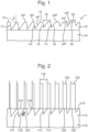
- a diffraction grating 1 comprises a glass substrate 10 on which there is a polymer layer 12.
- the layer 12 has impressed therein a series of grooves 14 in its top surface 15, the distance or pitch 16 between grooves 14 being such that the grooves 14 diffract a portion of the light incident thereon.
- d is the grating pitch
- ⁇ i is the angle of incidence of the light on the grating
- ⁇ m is the angle at which the light is diffracted relative to a normal to the grating
- ⁇ is the wavelength of the light
- m is an integer, which may be positive, negative or zero.
- the light is either transmitted though the grating 1 without diffraction or, in the case of a reflective grating, specularly reflected from the grating 1.
- the efficiency of the grating is the proportion of the incident light which is diffracted in the demand order (or orders, if the grating is to operate as a multiple order grating).
- the grating 1 of Figure 1 is a blazed grating i.e. one which is configured to have optimum efficiency for monochromatic light of a particular wavelength and at a particular range of incident angles.
- the grooves 14 have operative blazed surfaces 18 which are inclined to the surface 15 of the layer 12 so that they are perpendicular to the blaze angle ⁇ . This angle is chosen so that the grating 1 is most efficient at the operational wavelength and range of incident angles.
- the grooves 14 as illustrated are triangular in shape, and are formed by three facets: a blaze surface 18, a land surface 20 and a anti-blaze surface 17. It is usually required that blazed gratings diffract most efficiently in either the positive or negative orders.
- the anti-blaze facet 17 should be as perpendicular to the surface 15 as possible.
- the manufacturing process used to create a grating 1, which includes but is not limited to replication and coating, may dictate that the angle of the anti-blaze facet 17 deviates from perpendicular to the surface 15.
- the grooves 14 are of constant pitch 16. More specifically, their trailing edges 19 formed by the intersections of the blazed surfaces 18 with the surface 15 of the layer 12 are at constant pitch.
- the grooves are separated by lands 20 of predetermined width 22 which is chosen so as to vary from land to land.
- the geometry of the grooves 14 is constant, and consequently the depth of each groove 14 is determined by the width of its immediately-preceding land.
- groove 14' is preceded by a relatively narrow land 20' and thus is relatively deep.
- groove 14" is preceded by a relatively wide land 20" and thus is relatively shallow.
- pairs of adjacent lands e.g. 20' or 20" are shown to be of the same width, that width being different to the width of adjacent pairs of lands.
- Other patterns are of course possible: for example if each land 20 is of different width to its neighbours a more evenly graded variation in efficiency across the surface of the grating 1 can be obtained.
- a grating 1 with well-defined areas of different efficiency can be obtained. Indeed, if required a step-change between areas of marked by different efficiency can be achieved.
- Figure 1 is a section through the grating.
- the width of the lands 20 and the depth of the grooves 14 may also vary along their length, i.e. into or out of the plane of the figure. This enables the efficiency of for example the area 14", 20" and/or 14', 20' to be varied orthogonally to the variation from groove to groove.
- the variation in land width normally is effected during manufacture by maintaining the position of each intersection 19 between a blazed surface 18 and land 20 constant, and varying the land width away from it. Thereby the pitch 16 of the blazed surface edges 19 is held constant and the variation in groove depth is achieved.
- the pitch 16 of the grooves 14 may also be varied, if it is required for example to give the grating 1 optical power so that it operates also as a lens or non-planar mirror. This can enable errors in an image carried by the incident light to be corrected.
- the pitch 16 variation is set by adjusting the distance between successive edges 19, and the land 20 width is then set from the adjusted edges 19. Thus the efficiency variation is effectively superimposed on the pitch variations.
- the invention may also be applied to diffraction gratings defined on curved surfaces.
- Figure 2 illustrates manufacture of a master grating 110 for the replication of the diffraction grating 1 of Figure 1 .
- the master grating 110 comprises a crystal of silicon 112 disposed on a suitable substrate, not shown. When manufactured, the crystal has cut into its surface 115 grooves 114 of shape and pitch identical to those of the eventual grating 1, subject only to adjustments as will be familiar to those skilled in the art to allow for coatings which may be applied, and for dimensional changes which may arise during the replication process.
- the initially-planar surface 115 is provided with an etch-resistant mask by a known method.
- the surface 115 is coated with a film of a negative electron-beam resist 121 e.g. ZEP-520 (from "Zeon Corporation", Japan) or AR-N7700 (from “Allresist", Germany).
- This film is then traversed by a scanning electron beam 123 to expose the resist and forms a mask defining the lands 120.
- the width of the scanning pattern is varied so that the required variation in land 120 width is reproduced in the mask.
- the unexposed portions of the resist film 121 are then removed, and the thus-revealed portions of the surface 115 are subjected to anisotropic wet etching.
- the orientation of the silicon crystal 112 shown symbolically at 124, is chosen so that the blazed surfaces 118 lie parallel to a selected crystal plane of the silicon whereby the etch rate parallel to the crystal plane is much faster than the etch rate perpendicular to the crystal plane, thus defining the blazed surfaces 118 at the correct angle.
- the master grating 110 may be used to produce one or more replication moulds ("stampers") by known techniques, and the stampers in turn then used to produce diffraction gratings 1.
- a diffraction grating 1 includes a surface 12 having grooves 14 therein, each groove 14 is arranged to provide a diffracting surface for light incident upon the diffracting surface.
- the grooves 14 are separated from each other by lands 20 upon the surface 12.
- the lands 20 are of predetermined varying width, whereby the diffractive efficiency of the grating 1 varies across the extent or surface of the grating 1.
Landscapes
- Physics & Mathematics (AREA)
- General Physics & Mathematics (AREA)
- Optics & Photonics (AREA)
- Engineering & Computer Science (AREA)
- Manufacturing & Machinery (AREA)
- Diffracting Gratings Or Hologram Optical Elements (AREA)
Abstract
Description
- This invention relates to diffraction gratings and to the manufacture thereof.
- It sometimes is desirable that the efficiency of a diffraction grating should vary across its extent, so that the diffraction grating provides a differing effect in different regions of its surface. Usually this is achieved by controlling the thickness or other property of an optical coating applied to the surface of the grating. The degree of variation obtainable however may not to enough, or it may be insufficiently precise. At least in some embodiments the present invention can provide a variable-efficiency diffraction grating in which these problems are mitigated. The invention also provides a method of making the master gratings from which the diffraction gratings of the invention are replicated.
- In one aspect the invention provides a diffraction grating comprising a surface having grooves therein, each groove having a diffracting surface, the grooves being separated from each other by lands of the first-mentioned surface of predetermined varying width, whereby the diffractive efficiency of the grating varies across the extent of the grating.
- The grating may comprise blazed grooves in a surface, the grooves being separated by unblazed lands of the surface of predetermined varying width.
- The diffracting surfaces of the grooves may be disposed non-orthogonally to the first-mentioned surface.
- In particular, the grating may be a blazed grating.
- Thus, another aspect the invention provides a blazed diffraction grating comprising grooves in a surface, the grooves being separated by un-blazed lands of said surface of predetermined varying width.
- The lands may vary in width from groove to groove. By this we do not mean that each land is necessarily of different width to its immediate neighbours, although such a construction is within the invention. We also contemplate within this statement that groups of adjacent lands may have the same width, but this width may be different to that of a land or group of lands elsewhere on the grating.
- Alternatively or in addition a land may vary in width along its length.
- For a groove which tapers from top to bottom, for example a triangular groove of a blazed grating, the depth of the groove will be a function of its width. Thus, for grooves of constant pitch, increasing the width of the intervening lands decreases the width of the grooves and thus their depth. The efficiency of a grating with such grooves is a function of the groove depth, and so the local efficiency of a grating can be established by controlling the width of the groove-separating lands during manufacture of the grating. For gratings manufactured by replication this may be done by controlling the land width in the master grating.
- In this specification, the width of a groove or land is its dimension measured in the direction of successive pitches of the grating. The length of the groove or land is its longitudinal dimension locally orthogonal to the pitch dimension. The depth of a groove is its dimension into the surface in which it is defined.
- It will be appreciated from the foregoing that the depth of the groove may vary from groove to groove. Alternatively or in addition, a groove may vary in depth along its length.
- It also will be appreciated that the width of a land or land may be varied so that the pitch of the grooves may be varied across the extent of the grating. By this means it is possible, in addition or alternatively to varying the local efficiency of the grating, to introduce optical power into the grating for example to correct for angular distortion in an image transmitted or reflected by the grating.
- The invention also provides a master grating and/or replicator mould arranged to produce a grating as set forth above.
- The invention further provides a method of manufacturing such a master grating, comprising forming on a surface of a substrate a mask defining lands of varying width and removing unmasked material from the substrate to form grooves. When the substrate comprises a crystal, the method may comprising forming said surface of the substrate at an angle relative to a crystal plane of the substrate such that removal of the unmasked material is effected preferentially parallel to the crystal plane.
- The unmasked material may be removed by anisotropic wet etching.
- The invention will be described, merely by way of example only, with reference to the accompanying drawings, wherein:
-
Figure 1 is a section through a diffraction grating according to the invention; and -
Figure 2 illustrates the manufacture of a master grating according to the invention. - Referring to
Figure 1 , a diffraction grating 1 comprises a glass substrate 10 on which there is apolymer layer 12. Thelayer 12 has impressed therein a series ofgrooves 14 in itstop surface 15, the distance orpitch 16 betweengrooves 14 being such that thegrooves 14 diffract a portion of the light incident thereon. - The performance of a grating 1 in which the
grooves 14 are immediately adjacent each other is governed by the diffraction grating equation:
- Where d is the grating pitch, θi is the angle of incidence of the light on the grating, θm is the angle at which the light is diffracted relative to a normal to the grating, λ is the wavelength of the light and m is an integer, which may be positive, negative or zero.
- Generally, a grating 1 is configured so as to operate at a preferred order of diffraction e.g. m=1, 2 or -1, -2.
- When m=0 or "zero order" the light is either transmitted though the grating 1 without diffraction or, in the case of a reflective grating, specularly reflected from the grating 1.
- The efficiency of the grating is the proportion of the incident light which is diffracted in the demand order (or orders, if the grating is to operate as a multiple order grating).
- In this embodiment, the grating 1 of
Figure 1 is a blazed grating i.e. one which is configured to have optimum efficiency for monochromatic light of a particular wavelength and at a particular range of incident angles. Thus thegrooves 14 have operativeblazed surfaces 18 which are inclined to thesurface 15 of thelayer 12 so that they are perpendicular to the blaze angle β. This angle is chosen so that the grating 1 is most efficient at the operational wavelength and range of incident angles. Thegrooves 14 as illustrated are triangular in shape, and are formed by three facets: ablaze surface 18, aland surface 20 and aanti-blaze surface 17. It is usually required that blazed gratings diffract most efficiently in either the positive or negative orders. For this to happen, theanti-blaze facet 17 should be as perpendicular to thesurface 15 as possible. The manufacturing process used to create a grating 1, which includes but is not limited to replication and coating, may dictate that the angle of theanti-blaze facet 17 deviates from perpendicular to thesurface 15. - As noted, the
grooves 14 are ofconstant pitch 16. More specifically, theirtrailing edges 19 formed by the intersections of theblazed surfaces 18 with thesurface 15 of thelayer 12 are at constant pitch. However, according to the invention, the grooves are separated bylands 20 of predetermined width 22 which is chosen so as to vary from land to land. The geometry of thegrooves 14 is constant, and consequently the depth of eachgroove 14 is determined by the width of its immediately-preceding land. Thus it can be seen that groove 14' is preceded by a relatively narrow land 20' and thus is relatively deep. In contrast,groove 14" is preceded by a relativelywide land 20" and thus is relatively shallow. - This variation in land width and groove depth results in the diffraction efficiency of the grating 1 being different at different points on its
surface 15. Thus most of the light incident on the area defined by the land 20' and groove 14' will be received by the inclined blazed surface 18' and is diffracted into the desired order. Only the relatively small proportion of the incident light which is received by the land 20' is transmitted or reflected in the zero order, and thus the efficiency of this area of the grating 1 is relatively high. On the other hand, light incident on the area defined by theland 20" andgroove 14" will be received mostly by theland 20", and only a relatively small proportion by theblazed surface 18" of thegroove 14". Thus the efficiency of this area of the grating 1 will be relatively low. - In this particular embodiment pairs of adjacent lands e.g. 20' or 20" are shown to be of the same width, that width being different to the width of adjacent pairs of lands. Other patterns are of course possible: for example if each
land 20 is of different width to its neighbours a more evenly graded variation in efficiency across the surface of the grating 1 can be obtained. Alternatively, if substantial numbers ofadjacent lands 20 in one area of the grating 1 are of the same width, and substantial numbers ofadjacent lands 20 in another area of the grating 1 have a different width, then a grating 1 with well-defined areas of different efficiency can be obtained. Indeed, if required a step-change between areas of marked by different efficiency can be achieved. - As noted,
Figure 1 is a section through the grating. The width of thelands 20 and the depth of thegrooves 14 may also vary along their length, i.e. into or out of the plane of the figure. This enables the efficiency of for example thearea 14", 20" and/or 14', 20' to be varied orthogonally to the variation from groove to groove. - The variation in land width normally is effected during manufacture by maintaining the position of each
intersection 19 between a blazedsurface 18 andland 20 constant, and varying the land width away from it. Thereby thepitch 16 of the blazed surface edges 19 is held constant and the variation in groove depth is achieved. - It will be appreciated that the
pitch 16 of thegrooves 14 may also be varied, if it is required for example to give the grating 1 optical power so that it operates also as a lens or non-planar mirror. This can enable errors in an image carried by the incident light to be corrected. When designing a grating 1 having both varyingpitch 16 and varyingland 20 width, thepitch 16 variation is set by adjusting the distance betweensuccessive edges 19, and theland 20 width is then set from the adjusted edges 19. Thus the efficiency variation is effectively superimposed on the pitch variations. - Whilst the diffraction grating 1 has been described as planar, the invention may also be applied to diffraction gratings defined on curved surfaces.
-
Figure 2 illustrates manufacture of a master grating 110 for the replication of the diffraction grating 1 ofFigure 1 . - The master grating 110 comprises a crystal of
silicon 112 disposed on a suitable substrate, not shown. When manufactured, the crystal has cut into itssurface 115grooves 114 of shape and pitch identical to those of the eventual grating 1, subject only to adjustments as will be familiar to those skilled in the art to allow for coatings which may be applied, and for dimensional changes which may arise during the replication process. - To cut the
grooves 114, the initially-planar surface 115 is provided with an etch-resistant mask by a known method. Thus thesurface 115 is coated with a film of a negative electron-beam resist 121 e.g. ZEP-520 (from "Zeon Corporation", Japan) or AR-N7700 (from "Allresist", Germany). This film is then traversed by ascanning electron beam 123 to expose the resist and forms a mask defining thelands 120. The width of the scanning pattern is varied so that the required variation inland 120 width is reproduced in the mask. The unexposed portions of the resistfilm 121 are then removed, and the thus-revealed portions of thesurface 115 are subjected to anisotropic wet etching. To facilitate accurate and efficient etching the orientation of thesilicon crystal 112, shown symbolically at 124, is chosen so that the blazedsurfaces 118 lie parallel to a selected crystal plane of the silicon whereby the etch rate parallel to the crystal plane is much faster than the etch rate perpendicular to the crystal plane, thus defining the blazedsurfaces 118 at the correct angle. - Other known techniques may be used to provide the
grooves 114, for example ion beam milling, but this may not yield smooth crystalline surfaces, and the process may not control the blaze length and depth to the same degree as is obtainable by anisotropic wet etching of a suitably orientedcrystal 112 as described above. - The master grating 110 may be used to produce one or more replication moulds ("stampers") by known techniques, and the stampers in turn then used to produce diffraction gratings 1.
- A diffraction grating 1 includes a
surface 12 havinggrooves 14 therein, eachgroove 14 is arranged to provide a diffracting surface for light incident upon the diffracting surface. Thegrooves 14 are separated from each other bylands 20 upon thesurface 12. Thelands 20 are of predetermined varying width, whereby the diffractive efficiency of the grating 1 varies across the extent or surface of the grating 1. - The invention may be further understood by reference to the following numbered clauses:
- Clause 1. A diffraction grating comprising a surface having grooves therein, each groove having a diffracting surface, the grooves being separated from each other by lands of the first-mentioned surface of predetermined varying width, whereby the diffractive efficiency of the grating varies across the extent of the grating.
- Clause 2. The grating of clause 1 wherein the diffracting surface of the grooves are non-orthogonal to the first-mentioned surface.
- Clause 3. The grating of clause 1 or 2 comprising blazed grooves in a surface, the grooves being separated by unblazed lands of said surface of predetermined varying width.
- Clause 4. The grating of any preceding clause wherein the width of the lands varies from groove to groove.
- Clause 5. The grating of any preceding clause wherein the depth of the grooves varies from groove to groove.
- Clause 6. The grating of any preceding clause wherein the width of a said land varies along its length.
- Clause 7. The grating of any preceding clause wherein the depth of a said groove varies along its length.
- Clause 8. The grating of any preceding clause wherein the pitch of the grooves varies across the extent of the grating.
- Clause 9. A master grating or replicator mould arranged to produce the diffraction grating of any preceding clause.
- Clause 10. A method of manufacturing the master grating of clause 9, comprising forming on a surface of a substrate a mask defining lands of varying width and removing unmasked material from the substrate to form grooves.
- Clause 11. The method of clause 10 wherein the substrate comprises a crystal, the method comprising forming said surface of the substrate at an angle relative to a crystal plane of the substrate such that removal of the unmasked material is effected preferentially parallel to the crystal plane.
-
Clause 12. The method of clause 11 comprising removing the unmasked material by anisotropic wet etching. - Clause 13. A method of manufacturing a diffraction grating comprising replicating it from a master grating manufactured according to the method of any of clauses 11 to 12.
Claims (15)
- A method of manufacturing a diffraction grating, the method comprising:forming a layer on a substrate;impressing a plurality of blazed grooves in a first surface of the layer, each of the plurality of blazed grooves having a diffracting surface and an anti-blaze surface, each of the plurality of blazed grooves being separated from one another by lands of the first surface, the lands being defined by the blazed grooves and having a predetermined varying width, a diffractive efficiency of the grating varying across the first surface, the diffracting surface being inclined with respect to the first surface of the layer.
- The method of claim 1, wherein the plurality of grooves are impressed on the first surface by operations comprising:forming, on the first surface, a mask defining the lands of the varying width; andremoving unmasked material from the substrate thereby defining the grooves, each of the plurality of blazed grooves having a varied depth relative to the first surface, a depth of each of the plurality of blazed grooves being variable along a length thereof and further defined by a width of a land of the first surface adjacent to a respective groove, the width of the adjacent land varying along a length thereof, with a pitch distance between adjacent grooves being substantially constant along an axial length of the groove.
- The method of either claim 1 or claim 2, wherein:the layer comprises a polymer material; andthe substrate comprises a glass material.
- The method of either claim 1 or claim 2, wherein the substrate comprises a crystal having a crystal plane at an angle relative to the substrate such that the removing of the unmasked material is effected preferentially parallel to the crystal plane.
- The method of claim 4, wherein the removing of the unmasked material is performed by anisotropic wet etching.
- The method of claim 4, wherein the crystal is selected to be a crystal of silicon.
- The method of claim 2, wherein the mask is selected to be a film of a negative electron-beam resist.
- The method of any one of the preceding claims, further comprising forming the diffracting surface of the grooves to be non-orthogonal to the first surface of the layer.
- The method of any one of the preceding claims, further comprising forming the grooves to be separated by unblazed lands of the surface of a predetermined varying width.
- The method of any one of the preceding claims, further comprising forming the width of the lands to vary from groove to groove.
- The method of any one of the preceding claims, further comprising forming the depth of the lands to vary from groove to groove.
- The method of any one of the preceding claims, further comprising forming the pitch of the grooves to vary across the extent of the diffraction grating.
- The method of any one of the preceding claims, wherein the diffraction grating is formed to produce a master grating.
- The method of any one of claim 1 through claim 12, wherein the diffraction grating is formed to produce a replicator mould.
- A diffraction grating comprising a first surface having a plurality of blazed grooves therein, each of the plurality of blazed grooves having a diffracting surface and an anti-blaze surface, each of the plurality of blazed grooves being separated from one another by lands of the first surface, the lands being defined by the blazed grooves and having a predetermined varying width, a diffractive efficiency of the grating varying across the first surface, the diffracting surface being inclined with respect to the first surface of the layer.
Applications Claiming Priority (4)
| Application Number | Priority Date | Filing Date | Title |
|---|---|---|---|
| EP13275003.5A EP2752691A1 (en) | 2013-01-08 | 2013-01-08 | Variable-efficiency diffraction grating |
| GB1300239.9A GB2509536A (en) | 2013-01-08 | 2013-01-08 | Diffraction grating |
| PCT/GB2014/050019 WO2014108670A1 (en) | 2013-01-08 | 2014-01-06 | Diffraction gratings and the manufacture thereof |
| EP14700008.7A EP2943823B1 (en) | 2013-01-08 | 2014-01-06 | Diffraction gratings and the manufacture thereof |
Related Parent Applications (2)
| Application Number | Title | Priority Date | Filing Date |
|---|---|---|---|
| EP14700008.7A Division EP2943823B1 (en) | 2013-01-08 | 2014-01-06 | Diffraction gratings and the manufacture thereof |
| EP14700008.7A Division-Into EP2943823B1 (en) | 2013-01-08 | 2014-01-06 | Diffraction gratings and the manufacture thereof |
Publications (2)
| Publication Number | Publication Date |
|---|---|
| EP4556966A2 true EP4556966A2 (en) | 2025-05-21 |
| EP4556966A3 EP4556966A3 (en) | 2025-07-23 |
Family
ID=49917186
Family Applications (2)
| Application Number | Title | Priority Date | Filing Date |
|---|---|---|---|
| EP14700008.7A Active EP2943823B1 (en) | 2013-01-08 | 2014-01-06 | Diffraction gratings and the manufacture thereof |
| EP25168373.6A Pending EP4556966A3 (en) | 2013-01-08 | 2014-01-06 | Diffraction gratings and the manufacture thereof |
Family Applications Before (1)
| Application Number | Title | Priority Date | Filing Date |
|---|---|---|---|
| EP14700008.7A Active EP2943823B1 (en) | 2013-01-08 | 2014-01-06 | Diffraction gratings and the manufacture thereof |
Country Status (3)
| Country | Link |
|---|---|
| US (1) | US10422934B2 (en) |
| EP (2) | EP2943823B1 (en) |
| WO (1) | WO2014108670A1 (en) |
Families Citing this family (83)
| Publication number | Priority date | Publication date | Assignee | Title |
|---|---|---|---|---|
| GB0522968D0 (en) | 2005-11-11 | 2005-12-21 | Popovich Milan M | Holographic illumination device |
| GB0718706D0 (en) | 2007-09-25 | 2007-11-07 | Creative Physics Ltd | Method and apparatus for reducing laser speckle |
| US11726332B2 (en) | 2009-04-27 | 2023-08-15 | Digilens Inc. | Diffractive projection apparatus |
| US9335604B2 (en) | 2013-12-11 | 2016-05-10 | Milan Momcilo Popovich | Holographic waveguide display |
| US9274349B2 (en) | 2011-04-07 | 2016-03-01 | Digilens Inc. | Laser despeckler based on angular diversity |
| US10670876B2 (en) | 2011-08-24 | 2020-06-02 | Digilens Inc. | Waveguide laser illuminator incorporating a despeckler |
| EP2995986B1 (en) | 2011-08-24 | 2017-04-12 | Rockwell Collins, Inc. | Data display |
| WO2016020630A2 (en) | 2014-08-08 | 2016-02-11 | Milan Momcilo Popovich | Waveguide laser illuminator incorporating a despeckler |
| WO2013102759A2 (en) | 2012-01-06 | 2013-07-11 | Milan Momcilo Popovich | Contact image sensor using switchable bragg gratings |
| WO2013163347A1 (en) | 2012-04-25 | 2013-10-31 | Rockwell Collins, Inc. | Holographic wide angle display |
| US9456744B2 (en) | 2012-05-11 | 2016-10-04 | Digilens, Inc. | Apparatus for eye tracking |
| US9933684B2 (en) | 2012-11-16 | 2018-04-03 | Rockwell Collins, Inc. | Transparent waveguide display providing upper and lower fields of view having a specific light output aperture configuration |
| EP2943823B1 (en) | 2013-01-08 | 2025-05-07 | Snap Inc. | Diffraction gratings and the manufacture thereof |
| WO2014188149A1 (en) | 2013-05-20 | 2014-11-27 | Milan Momcilo Popovich | Holographic waveguide eye tracker |
| US9727772B2 (en) | 2013-07-31 | 2017-08-08 | Digilens, Inc. | Method and apparatus for contact image sensing |
| US10359736B2 (en) | 2014-08-08 | 2019-07-23 | Digilens Inc. | Method for holographic mastering and replication |
| US10241330B2 (en) | 2014-09-19 | 2019-03-26 | Digilens, Inc. | Method and apparatus for generating input images for holographic waveguide displays |
| EP3198192A1 (en) | 2014-09-26 | 2017-08-02 | Milan Momcilo Popovich | Holographic waveguide opticaltracker |
| WO2016113533A2 (en) | 2015-01-12 | 2016-07-21 | Milan Momcilo Popovich | Holographic waveguide light field displays |
| EP3245444B1 (en) | 2015-01-12 | 2021-09-08 | DigiLens Inc. | Environmentally isolated waveguide display |
| WO2016116733A1 (en) | 2015-01-20 | 2016-07-28 | Milan Momcilo Popovich | Holographic waveguide lidar |
| US9632226B2 (en) | 2015-02-12 | 2017-04-25 | Digilens Inc. | Waveguide grating device |
| WO2016146963A1 (en) | 2015-03-16 | 2016-09-22 | Popovich, Milan, Momcilo | Waveguide device incorporating a light pipe |
| US10591756B2 (en) | 2015-03-31 | 2020-03-17 | Digilens Inc. | Method and apparatus for contact image sensing |
| US9910276B2 (en) * | 2015-06-30 | 2018-03-06 | Microsoft Technology Licensing, Llc | Diffractive optical elements with graded edges |
| US10670862B2 (en) | 2015-07-02 | 2020-06-02 | Microsoft Technology Licensing, Llc | Diffractive optical elements with asymmetric profiles |
| US9864208B2 (en) | 2015-07-30 | 2018-01-09 | Microsoft Technology Licensing, Llc | Diffractive optical elements with varying direction for depth modulation |
| US10038840B2 (en) | 2015-07-30 | 2018-07-31 | Microsoft Technology Licensing, Llc | Diffractive optical element using crossed grating for pupil expansion |
| US10073278B2 (en) | 2015-08-27 | 2018-09-11 | Microsoft Technology Licensing, Llc | Diffractive optical element using polarization rotation grating for in-coupling |
| NL2017275A (en) | 2015-09-03 | 2017-03-08 | Asml Netherlands Bv | Beam splitting apparatus |
| CN113759555B (en) | 2015-10-05 | 2024-09-20 | 迪吉伦斯公司 | Waveguide Display |
| US10429645B2 (en) | 2015-10-07 | 2019-10-01 | Microsoft Technology Licensing, Llc | Diffractive optical element with integrated in-coupling, exit pupil expansion, and out-coupling |
| US10241332B2 (en) | 2015-10-08 | 2019-03-26 | Microsoft Technology Licensing, Llc | Reducing stray light transmission in near eye display using resonant grating filter |
| US9946072B2 (en) | 2015-10-29 | 2018-04-17 | Microsoft Technology Licensing, Llc | Diffractive optical element with uncoupled grating structures |
| US10234686B2 (en) | 2015-11-16 | 2019-03-19 | Microsoft Technology Licensing, Llc | Rainbow removal in near-eye display using polarization-sensitive grating |
| US10373544B1 (en) * | 2016-01-29 | 2019-08-06 | Leia, Inc. | Transformation from tiled to composite images |
| US10983340B2 (en) | 2016-02-04 | 2021-04-20 | Digilens Inc. | Holographic waveguide optical tracker |
| WO2017162999A1 (en) | 2016-03-24 | 2017-09-28 | Popovich Milan Momcilo | Method and apparatus for providing a polarization selective holographic waveguide device |
| US10890707B2 (en) | 2016-04-11 | 2021-01-12 | Digilens Inc. | Holographic waveguide apparatus for structured light projection |
| WO2017212522A1 (en) * | 2016-06-06 | 2017-12-14 | 株式会社島津製作所 | Diffraction grating and spectral device |
| CN106125176B (en) * | 2016-07-11 | 2018-06-26 | 中国科学院上海技术物理研究所 | A kind of one-dimensional three-dimensional phase grating of Terahertz |
| JP6958120B2 (en) * | 2016-08-29 | 2021-11-02 | 大日本印刷株式会社 | Diffractive optical element, light irradiation device |
| CN107870382B (en) | 2016-09-26 | 2019-11-05 | 京东方科技集团股份有限公司 | A kind of slit grating and three-dimensional display apparatus |
| EP3548939A4 (en) | 2016-12-02 | 2020-11-25 | DigiLens Inc. | WAVE GUIDE DEVICE WITH UNIFORM OUTPUT LIGHTING |
| CN106842397B (en) * | 2017-01-05 | 2020-07-17 | 苏州苏大维格光电科技股份有限公司 | A resin holographic waveguide lens, a preparation method thereof, and a three-dimensional display device |
| WO2018129398A1 (en) | 2017-01-05 | 2018-07-12 | Digilens, Inc. | Wearable heads up displays |
| US10108014B2 (en) * | 2017-01-10 | 2018-10-23 | Microsoft Technology Licensing, Llc | Waveguide display with multiple focal depths |
| CN108802878B (en) * | 2017-04-27 | 2021-02-26 | 清华大学 | Pine-like metal nanogratings |
| US10942430B2 (en) | 2017-10-16 | 2021-03-09 | Digilens Inc. | Systems and methods for multiplying the image resolution of a pixelated display |
| US10914950B2 (en) | 2018-01-08 | 2021-02-09 | Digilens Inc. | Waveguide architectures and related methods of manufacturing |
| US10732569B2 (en) | 2018-01-08 | 2020-08-04 | Digilens Inc. | Systems and methods for high-throughput recording of holographic gratings in waveguide cells |
| US20190212588A1 (en) | 2018-01-08 | 2019-07-11 | Digilens, Inc. | Systems and Methods for Manufacturing Waveguide Cells |
| KR20250004154A (en) | 2018-01-08 | 2025-01-07 | 디지렌즈 인코포레이티드. | Methods for fabricating optical waveguides |
| CN108444913A (en) * | 2018-01-30 | 2018-08-24 | 中国科学院上海技术物理研究所 | Based on unit born of the same parents' solid phase grating and mutually with reference to the THz spectrometers of technology |
| CN112088332B (en) | 2018-03-16 | 2024-11-29 | 迪吉伦斯公司 | Holographic waveguides comprising birefringence control and methods for their manufacture |
| WO2020023779A1 (en) | 2018-07-25 | 2020-01-30 | Digilens Inc. | Systems and methods for fabricating a multilayer optical structure |
| CN109212641B (en) * | 2018-09-29 | 2021-07-13 | 中国科学院微电子研究所 | A phase diffraction grating |
| US10690831B2 (en) * | 2018-11-20 | 2020-06-23 | Facebook Technologies, Llc | Anisotropically formed diffraction grating device |
| US10690821B1 (en) * | 2018-12-14 | 2020-06-23 | Applied Materials, Inc. | Methods of producing slanted gratings |
| WO2020149956A1 (en) | 2019-01-14 | 2020-07-23 | Digilens Inc. | Holographic waveguide display with light control layer |
| US20200247017A1 (en) | 2019-02-05 | 2020-08-06 | Digilens Inc. | Methods for Compensating for Optical Surface Nonuniformity |
| JP7259381B2 (en) * | 2019-02-12 | 2023-04-18 | 凸版印刷株式会社 | Labels, plates, transfer foils, adhesive labels and articles with labels |
| CN113692544B (en) | 2019-02-15 | 2025-04-22 | 迪吉伦斯公司 | Method and apparatus for providing holographic waveguide displays using integrated gratings |
| US20220283377A1 (en) | 2019-02-15 | 2022-09-08 | Digilens Inc. | Wide Angle Waveguide Display |
| US10976483B2 (en) * | 2019-02-26 | 2021-04-13 | Facebook Technologies, Llc | Variable-etch-depth gratings |
| US20200292745A1 (en) | 2019-03-12 | 2020-09-17 | Digilens Inc. | Holographic Waveguide Backlight and Related Methods of Manufacturing |
| EP3719545A1 (en) * | 2019-04-03 | 2020-10-07 | ASML Netherlands B.V. | Manufacturing a reflective diffraction grating |
| US10809448B1 (en) * | 2019-04-18 | 2020-10-20 | Facebook Technologies, Llc | Reducing demolding stress at edges of gratings in nanoimprint lithography |
| CN114207492A (en) | 2019-06-07 | 2022-03-18 | 迪吉伦斯公司 | Waveguide with transmission grating and reflection grating and method for producing the same |
| US11681143B2 (en) | 2019-07-29 | 2023-06-20 | Digilens Inc. | Methods and apparatus for multiplying the image resolution and field-of-view of a pixelated display |
| KR102775783B1 (en) | 2019-08-29 | 2025-02-28 | 디지렌즈 인코포레이티드. | Vacuum grid and method for manufacturing the same |
| CN114174872B (en) * | 2019-08-29 | 2023-10-17 | 株式会社日立高新技术 | Diffraction grating, method for manufacturing diffraction grating, and photomask |
| JP7487482B2 (en) * | 2020-02-05 | 2024-05-21 | Toppanホールディングス株式会社 | Color Shifting Device |
| CN111880254B (en) * | 2020-07-14 | 2021-05-14 | 浙江大学 | Preparation method of grating with continuously-changed diffraction efficiency |
| US11709422B2 (en) | 2020-09-17 | 2023-07-25 | Meta Platforms Technologies, Llc | Gray-tone lithography for precise control of grating etch depth |
| FI130396B (en) * | 2020-09-23 | 2023-08-10 | Dispelix Oy | Optical Waveguide for Augmented Reality Display |
| JP2024502255A (en) | 2020-12-21 | 2024-01-18 | ディジレンズ インコーポレイテッド | Eye glow suppression in waveguide-based displays |
| FI130103B (en) | 2020-12-22 | 2023-03-01 | Dispelix Oy | Diffractive optical element grating stamper and master model manufacturing method, master model and stamper |
| WO2022150841A1 (en) | 2021-01-07 | 2022-07-14 | Digilens Inc. | Grating structures for color waveguides |
| EP4288831A4 (en) | 2021-03-05 | 2025-01-15 | Digilens Inc. | EVACUATED PERIODIC STRUCTURES AND THEIR MANUFACTURING PROCESSES |
| US20240264353A1 (en) * | 2023-02-03 | 2024-08-08 | Apple Inc. | Display Devices Having Gratings With Gradient Edges |
| CN116500712A (en) * | 2023-04-24 | 2023-07-28 | 清华大学 | Gradient Sparkle Surface Grating |
| WO2024258833A1 (en) | 2023-06-12 | 2024-12-19 | Snap Inc. | Optical waveguide manufacturing method |
Family Cites Families (18)
| Publication number | Priority date | Publication date | Assignee | Title |
|---|---|---|---|---|
| US2533077A (en) * | 1947-10-15 | 1950-12-05 | Larkin R Williamson | Gear reduction mechanism for press brakes |
| US3980883A (en) * | 1973-05-15 | 1976-09-14 | National Research Development Corporation | X-ray diffraction gratings |
| US4606640A (en) * | 1984-04-02 | 1986-08-19 | The Perkin-Elmer Corporation | Method and apparatus for optically testing cylindrical surfaces |
| US4798446A (en) * | 1987-09-14 | 1989-01-17 | The United States Of America As Represented By The United States Department Of Energy | Aplanatic and quasi-aplanatic diffraction gratings |
| ATE114826T1 (en) * | 1988-03-18 | 1994-12-15 | Instruments Sa | DIFFRACTION GRATINGS AND MANUFACTURING METHOD THEREOF. |
| US5279924A (en) | 1989-04-04 | 1994-01-18 | Sharp Kabushiki Kaisha | Manufacturing method of optical diffraction grating element with serrated gratings having uniformly etched grooves |
| US5283690A (en) | 1989-04-04 | 1994-02-01 | Sharp Kabushiki Kaisha | Optical diffraction grating element |
| CA2029674C (en) * | 1989-11-13 | 1997-06-10 | Keiji Sakai | Manufacturing method of optical diffraction grating element |
| JPH1026707A (en) * | 1996-07-11 | 1998-01-27 | Sanyo Electric Co Ltd | Surface relief type diffraction grating and its manufacture |
| US6961490B2 (en) | 2000-01-27 | 2005-11-01 | Unaxis-Balzers Aktiengesellschaft | Waveguide plate and process for its production and microtitre plate |
| US6400509B1 (en) * | 2000-04-07 | 2002-06-04 | Zolo Technologies, Inc. | Apparatus and method for the reduction of polarization sensitivity in diffraction gratings used in fiber optic communications devices |
| US7375887B2 (en) * | 2001-03-27 | 2008-05-20 | Moxtek, Inc. | Method and apparatus for correcting a visible light beam using a wire-grid polarizer |
| US7315502B2 (en) * | 2001-11-09 | 2008-01-01 | Sharp Kabushiki Kaisha | Light integration unit, optical pickup device using the unit, and optical disk device |
| JP4358583B2 (en) * | 2003-09-12 | 2009-11-04 | 株式会社ミツトヨ | Scale manufacturing method |
| DE102005027380B4 (en) * | 2005-06-14 | 2009-04-30 | Ovd Kinegram Ag | The security document |
| JP4990351B2 (en) * | 2007-02-26 | 2012-08-01 | 三菱電機株式会社 | Optical pickup device |
| EP2533077A1 (en) * | 2011-06-08 | 2012-12-12 | Nederlandse Organisatie voor toegepast -natuurwetenschappelijk onderzoek TNO | Diffraction grating and method for producing same |
| EP2943823B1 (en) | 2013-01-08 | 2025-05-07 | Snap Inc. | Diffraction gratings and the manufacture thereof |
-
2014
- 2014-01-06 EP EP14700008.7A patent/EP2943823B1/en active Active
- 2014-01-06 EP EP25168373.6A patent/EP4556966A3/en active Pending
- 2014-01-06 US US14/653,618 patent/US10422934B2/en active Active
- 2014-01-06 WO PCT/GB2014/050019 patent/WO2014108670A1/en not_active Ceased
Also Published As
| Publication number | Publication date |
|---|---|
| WO2014108670A1 (en) | 2014-07-17 |
| US20150355394A1 (en) | 2015-12-10 |
| EP4556966A3 (en) | 2025-07-23 |
| US10422934B2 (en) | 2019-09-24 |
| EP2943823B1 (en) | 2025-05-07 |
| EP2943823A1 (en) | 2015-11-18 |
Similar Documents
| Publication | Publication Date | Title |
|---|---|---|
| EP2943823B1 (en) | Diffraction gratings and the manufacture thereof | |
| EP2752691A1 (en) | Variable-efficiency diffraction grating | |
| GB2509536A (en) | Diffraction grating | |
| US11686890B2 (en) | Multi-level diffractive optical element thin film coating | |
| TWI440833B (en) | Hybrid diffraction grating, mold insert, and methods of manufacturing such grating and mold insert | |
| US11543562B2 (en) | Multi-layer thin film stack for diffractive optical elements | |
| US20040032667A1 (en) | Technique for microstructuring replication mold | |
| CN110998375A (en) | Method and motherboard for making a motherboard | |
| US20190079395A1 (en) | Manufacturing method of diffractive optical elements | |
| CN102360092A (en) | Optical element and method for manufacturing the same | |
| WO2019130835A1 (en) | Method for manufacturingconcave diffraction grating, concave diffraction grating, and analysis device using same | |
| EP3289396A1 (en) | Partially etched phase-transforming optical element | |
| JP2005084485A (en) | Diffractive optical element | |
| JP2010102008A (en) | Photomask and method for making sawtooth pattern | |
| HK40126435A (en) | Diffraction gratings and the manufacture thereof | |
| JP2008112036A (en) | Manufacturing method of fine structure | |
| CN103901515A (en) | Rectangular quartz double-polarization blazed grating with 532 nanometer wave band | |
| EP2199837B1 (en) | A dispersion grating | |
| US20060077554A1 (en) | Diffraction gratings for electromagnetic radiation, and a method of production | |
| JP6547283B2 (en) | Method of manufacturing structure on substrate | |
| JP4495722B2 (en) | Microstructure creation method | |
| JP2005037868A (en) | Method for forming antireflection face, method for manufacturing mold for forming antireflection member, mold, antireflection member, and method for manufacturing master member for manufacturing mold | |
| CN109061781B (en) | Method for photoetching binary harmonic diffraction Alvarez lens zoom system | |
| CN111741839B (en) | Method for manufacturing mold | |
| JPS59210403A (en) | How to make a diffraction grating |
Legal Events
| Date | Code | Title | Description |
|---|---|---|---|
| PUAI | Public reference made under article 153(3) epc to a published international application that has entered the european phase |
Free format text: ORIGINAL CODE: 0009012 |
|
| STAA | Information on the status of an ep patent application or granted ep patent |
Free format text: STATUS: REQUEST FOR EXAMINATION WAS MADE |
|
| 17P | Request for examination filed |
Effective date: 20250407 |
|
| AC | Divisional application: reference to earlier application |
Ref document number: 2943823 Country of ref document: EP Kind code of ref document: P |
|
| AK | Designated contracting states |
Kind code of ref document: A2 Designated state(s): AL AT BE BG CH CY CZ DE DK EE ES FI FR GB GR HR HU IE IS IT LI LT LU LV MC MK MT NL NO PL PT RO RS SE SI SK SM TR |
|
| PUAL | Search report despatched |
Free format text: ORIGINAL CODE: 0009013 |
|
| AK | Designated contracting states |
Kind code of ref document: A3 Designated state(s): AL AT BE BG CH CY CZ DE DK EE ES FI FR GB GR HR HU IE IS IT LI LT LU LV MC MK MT NL NO PL PT RO RS SE SI SK SM TR |
|
| RIC1 | Information provided on ipc code assigned before grant |
Ipc: G02B 5/18 20060101AFI20250613BHEP |
|
| REG | Reference to a national code |
Ref country code: HK Ref legal event code: DE Ref document number: 40126435 Country of ref document: HK |