EP4546984A2 - Mikro-led, mikro-led-array-tafel und herstellungsverfahren dafür - Google Patents
Mikro-led, mikro-led-array-tafel und herstellungsverfahren dafür Download PDFInfo
- Publication number
- EP4546984A2 EP4546984A2 EP25151773.6A EP25151773A EP4546984A2 EP 4546984 A2 EP4546984 A2 EP 4546984A2 EP 25151773 A EP25151773 A EP 25151773A EP 4546984 A2 EP4546984 A2 EP 4546984A2
- Authority
- EP
- European Patent Office
- Prior art keywords
- type semiconductor
- semiconductor layer
- fence
- ion implantation
- trench
- Prior art date
- Legal status (The legal status is an assumption and is not a legal conclusion. Google has not performed a legal analysis and makes no representation as to the accuracy of the status listed.)
- Pending
Links
Images


Classifications
-
- H—ELECTRICITY
- H10—SEMICONDUCTOR DEVICES; ELECTRIC SOLID-STATE DEVICES NOT OTHERWISE PROVIDED FOR
- H10H—INORGANIC LIGHT-EMITTING SEMICONDUCTOR DEVICES HAVING POTENTIAL BARRIERS
- H10H20/00—Individual inorganic light-emitting semiconductor devices having potential barriers, e.g. light-emitting diodes [LED]
- H10H20/80—Constructional details
- H10H20/81—Bodies
- H10H20/819—Bodies characterised by their shape, e.g. curved or truncated substrates
- H10H20/821—Bodies characterised by their shape, e.g. curved or truncated substrates of the light-emitting regions, e.g. non-planar junctions
-
- H—ELECTRICITY
- H10—SEMICONDUCTOR DEVICES; ELECTRIC SOLID-STATE DEVICES NOT OTHERWISE PROVIDED FOR
- H10H—INORGANIC LIGHT-EMITTING SEMICONDUCTOR DEVICES HAVING POTENTIAL BARRIERS
- H10H20/00—Individual inorganic light-emitting semiconductor devices having potential barriers, e.g. light-emitting diodes [LED]
- H10H20/80—Constructional details
- H10H20/81—Bodies
- H10H20/816—Bodies having carrier transport control structures, e.g. highly-doped semiconductor layers or current-blocking structures
- H10H20/8162—Current-blocking structures
-
- H—ELECTRICITY
- H10—SEMICONDUCTOR DEVICES; ELECTRIC SOLID-STATE DEVICES NOT OTHERWISE PROVIDED FOR
- H10H—INORGANIC LIGHT-EMITTING SEMICONDUCTOR DEVICES HAVING POTENTIAL BARRIERS
- H10H20/00—Individual inorganic light-emitting semiconductor devices having potential barriers, e.g. light-emitting diodes [LED]
- H10H20/01—Manufacture or treatment
- H10H20/011—Manufacture or treatment of bodies, e.g. forming semiconductor layers
- H10H20/013—Manufacture or treatment of bodies, e.g. forming semiconductor layers having light-emitting regions comprising only Group III-V materials
- H10H20/0133—Manufacture or treatment of bodies, e.g. forming semiconductor layers having light-emitting regions comprising only Group III-V materials with a substrate not being Group III-V materials
- H10H20/01335—Manufacture or treatment of bodies, e.g. forming semiconductor layers having light-emitting regions comprising only Group III-V materials with a substrate not being Group III-V materials the light-emitting regions comprising nitride materials
-
- H—ELECTRICITY
- H10—SEMICONDUCTOR DEVICES; ELECTRIC SOLID-STATE DEVICES NOT OTHERWISE PROVIDED FOR
- H10H—INORGANIC LIGHT-EMITTING SEMICONDUCTOR DEVICES HAVING POTENTIAL BARRIERS
- H10H20/00—Individual inorganic light-emitting semiconductor devices having potential barriers, e.g. light-emitting diodes [LED]
- H10H20/01—Manufacture or treatment
- H10H20/011—Manufacture or treatment of bodies, e.g. forming semiconductor layers
- H10H20/013—Manufacture or treatment of bodies, e.g. forming semiconductor layers having light-emitting regions comprising only Group III-V materials
- H10H20/0137—Manufacture or treatment of bodies, e.g. forming semiconductor layers having light-emitting regions comprising only Group III-V materials the light-emitting regions comprising nitride materials
-
- H—ELECTRICITY
- H10—SEMICONDUCTOR DEVICES; ELECTRIC SOLID-STATE DEVICES NOT OTHERWISE PROVIDED FOR
- H10H—INORGANIC LIGHT-EMITTING SEMICONDUCTOR DEVICES HAVING POTENTIAL BARRIERS
- H10H20/00—Individual inorganic light-emitting semiconductor devices having potential barriers, e.g. light-emitting diodes [LED]
- H10H20/80—Constructional details
- H10H20/81—Bodies
- H10H20/819—Bodies characterised by their shape, e.g. curved or truncated substrates
-
- H—ELECTRICITY
- H10—SEMICONDUCTOR DEVICES; ELECTRIC SOLID-STATE DEVICES NOT OTHERWISE PROVIDED FOR
- H10H—INORGANIC LIGHT-EMITTING SEMICONDUCTOR DEVICES HAVING POTENTIAL BARRIERS
- H10H20/00—Individual inorganic light-emitting semiconductor devices having potential barriers, e.g. light-emitting diodes [LED]
- H10H20/80—Constructional details
- H10H20/81—Bodies
- H10H20/822—Materials of the light-emitting regions
- H10H20/824—Materials of the light-emitting regions comprising only Group III-V materials, e.g. GaP
- H10H20/825—Materials of the light-emitting regions comprising only Group III-V materials, e.g. GaP containing nitrogen, e.g. GaN
-
- H—ELECTRICITY
- H10—SEMICONDUCTOR DEVICES; ELECTRIC SOLID-STATE DEVICES NOT OTHERWISE PROVIDED FOR
- H10H—INORGANIC LIGHT-EMITTING SEMICONDUCTOR DEVICES HAVING POTENTIAL BARRIERS
- H10H20/00—Individual inorganic light-emitting semiconductor devices having potential barriers, e.g. light-emitting diodes [LED]
- H10H20/80—Constructional details
- H10H20/83—Electrodes
- H10H20/831—Electrodes characterised by their shape
-
- H—ELECTRICITY
- H10—SEMICONDUCTOR DEVICES; ELECTRIC SOLID-STATE DEVICES NOT OTHERWISE PROVIDED FOR
- H10H—INORGANIC LIGHT-EMITTING SEMICONDUCTOR DEVICES HAVING POTENTIAL BARRIERS
- H10H20/00—Individual inorganic light-emitting semiconductor devices having potential barriers, e.g. light-emitting diodes [LED]
- H10H20/80—Constructional details
- H10H20/84—Coatings, e.g. passivation layers or antireflective coatings
-
- H—ELECTRICITY
- H10—SEMICONDUCTOR DEVICES; ELECTRIC SOLID-STATE DEVICES NOT OTHERWISE PROVIDED FOR
- H10H—INORGANIC LIGHT-EMITTING SEMICONDUCTOR DEVICES HAVING POTENTIAL BARRIERS
- H10H20/00—Individual inorganic light-emitting semiconductor devices having potential barriers, e.g. light-emitting diodes [LED]
- H10H20/80—Constructional details
- H10H20/85—Packages
- H10H20/855—Optical field-shaping means, e.g. lenses
-
- H—ELECTRICITY
- H10—SEMICONDUCTOR DEVICES; ELECTRIC SOLID-STATE DEVICES NOT OTHERWISE PROVIDED FOR
- H10H—INORGANIC LIGHT-EMITTING SEMICONDUCTOR DEVICES HAVING POTENTIAL BARRIERS
- H10H20/00—Individual inorganic light-emitting semiconductor devices having potential barriers, e.g. light-emitting diodes [LED]
- H10H20/80—Constructional details
- H10H20/85—Packages
- H10H20/857—Interconnections, e.g. lead-frames, bond wires or solder balls
-
- H—ELECTRICITY
- H10—SEMICONDUCTOR DEVICES; ELECTRIC SOLID-STATE DEVICES NOT OTHERWISE PROVIDED FOR
- H10H—INORGANIC LIGHT-EMITTING SEMICONDUCTOR DEVICES HAVING POTENTIAL BARRIERS
- H10H29/00—Integrated devices, or assemblies of multiple devices, comprising at least one light-emitting semiconductor element covered by group H10H20/00
- H10H29/10—Integrated devices comprising at least one light-emitting semiconductor component covered by group H10H20/00
- H10H29/14—Integrated devices comprising at least one light-emitting semiconductor component covered by group H10H20/00 comprising multiple light-emitting semiconductor components
-
- H10W90/00—
-
- H—ELECTRICITY
- H10—SEMICONDUCTOR DEVICES; ELECTRIC SOLID-STATE DEVICES NOT OTHERWISE PROVIDED FOR
- H10H—INORGANIC LIGHT-EMITTING SEMICONDUCTOR DEVICES HAVING POTENTIAL BARRIERS
- H10H20/00—Individual inorganic light-emitting semiconductor devices having potential barriers, e.g. light-emitting diodes [LED]
- H10H20/01—Manufacture or treatment
- H10H20/011—Manufacture or treatment of bodies, e.g. forming semiconductor layers
- H10H20/017—Etching
-
- H—ELECTRICITY
- H10—SEMICONDUCTOR DEVICES; ELECTRIC SOLID-STATE DEVICES NOT OTHERWISE PROVIDED FOR
- H10H—INORGANIC LIGHT-EMITTING SEMICONDUCTOR DEVICES HAVING POTENTIAL BARRIERS
- H10H20/00—Individual inorganic light-emitting semiconductor devices having potential barriers, e.g. light-emitting diodes [LED]
- H10H20/01—Manufacture or treatment
- H10H20/011—Manufacture or treatment of bodies, e.g. forming semiconductor layers
- H10H20/018—Bonding of wafers
-
- H—ELECTRICITY
- H10—SEMICONDUCTOR DEVICES; ELECTRIC SOLID-STATE DEVICES NOT OTHERWISE PROVIDED FOR
- H10H—INORGANIC LIGHT-EMITTING SEMICONDUCTOR DEVICES HAVING POTENTIAL BARRIERS
- H10H20/00—Individual inorganic light-emitting semiconductor devices having potential barriers, e.g. light-emitting diodes [LED]
- H10H20/01—Manufacture or treatment
- H10H20/011—Manufacture or treatment of bodies, e.g. forming semiconductor layers
- H10H20/019—Removal of at least a part of a substrate on which semiconductor layers have been formed
-
- H—ELECTRICITY
- H10—SEMICONDUCTOR DEVICES; ELECTRIC SOLID-STATE DEVICES NOT OTHERWISE PROVIDED FOR
- H10H—INORGANIC LIGHT-EMITTING SEMICONDUCTOR DEVICES HAVING POTENTIAL BARRIERS
- H10H20/00—Individual inorganic light-emitting semiconductor devices having potential barriers, e.g. light-emitting diodes [LED]
- H10H20/01—Manufacture or treatment
- H10H20/036—Manufacture or treatment of packages
- H10H20/0364—Manufacture or treatment of packages of interconnections
Definitions
- the present disclosure generally relates to light emitting diode, and more particularly, to a micro light emitting diode (LED), a micro LED array panel, and a manufacturing method thereof.
- LED micro light emitting diode
- micro LEDs Inorganic micro pixel light emitting diodes, also referred to as micro light emitting diodes, micro LEDs or ⁇ -LEDs, are of increasing importance because of their use in various applications including self-emissive micro-displays, visible light communications, and optogenetics.
- the micro LEDs exhibit higher output performance than conventional LEDs due to better strain relaxation, improved light extraction efficiency, and uniform current spreading.
- the micro LEDs also exhibit improved thermal effects, fast response rate, larger work temperature range, higher resolution, color gamut and contrast, and lower power consumption, and can be operated at higher current density compared with conventional LEDs.
- the inorganic micro LEDs are conventionally III -V group epitaxial layers formed as multiple mesas.
- a space is formed between the adjacent micro LEDs in the conventional micro LEDs structures to avoid carriers in the epitaxial layer spreading from one mesa to an adjacent mesa.
- the space which is formed between the adjacent micro LEDs can reduce an active light emitting area and decrease light extraction efficiency. If there is no space between the adjacent micro LEDs, the active light emitting area would be increased and the carriers in the epitaxial layer would spread laterally to the adjacent mesa, which reduces the light emitting efficiency of the micro LED. Furthermore, if there is no space formed between the adjacent mesas, cross talk will be produced between the adjacent micro LEDs, which would interfere with micro LEDs operation.
- Embodiments of the present disclosure provide a micro LED.
- the micro LED includes a first type semiconductor layer; and a light emitting layer formed on the first type semiconductor layer; wherein the first type semiconductor layer includes a mesa structure, a trench, and an ion implantation fence separated from the mesa structure, the trench extending up through the first type semiconductor layer and extending up into at least part of the light emitting layer; and the ion implantation fence is formed around the trench and the trench is formed around the mesa structure; wherein an electrical resistance of the ion implantation fence is higher than an electrical resistance of the mesa structure.
- Embodiments of the present disclosure provide a method for manufacturing a micro LED.
- the method includes providing an epitaxial structure, wherein the epitaxial structure includes a first type semiconductor layer, a light emitting layer, and a second type semiconductor layer sequentially from top to bottom; patterning the first type semiconductor layer to form a mesa structure, a trench, and a fence; depositing a bottom contact on the mesa structure; and performing an ion implantation process into the fence to form a first ion implantation fence.
- Embodiments of the present disclosure provide a micro LED.
- the micro LED includes a first type semiconductor layer; and a light emitting layer formed on the first type semiconductor layer; a second type semiconductor layer formed on the light emitting layer; an integrated circuit (IC) backplane formed at a bottom surface of the first type semiconductor layer; wherein the second type semiconductor layer includes a mesa structure, a trench, and an ion implantation fence separated from the mesa structure, the trench extending down through the second type semiconductor layer and extending down into at least part of the light emitting layer; and the ion implantation fence is formed around the trench and the trench is formed around the mesa structure, wherein and an electrical resistance of the ion implantation fence is higher than an electrical resistance of the mesa structure.
- IC integrated circuit
- Embodiments of the present disclosure provide a method for manufacturing a micro LED.
- the method includes providing an epitaxial structure, wherein the epitaxial structure includes a first type semiconductor layer, a light emitting layer, and a second type semiconductor layer sequentially from top to bottom; bonding the epitaxial structure with an integrated circuit (IC) backplane; patterning the second type semiconductor layer to form a mesa structure, a trench, and a fence; depositing a top contact on the mesa structure; performing an ion implantation process into the fence; depositing a top conductive layer on a top surface of the second type semiconductor layer, on a top contact, and in the trench.
- IC integrated circuit
- Embodiments of the present disclosure provide a micro LED.
- the micro LED includes a first type semiconductor layer; a light emitting layer formed on the first type semiconductor layer; and a second type semiconductor layer formed on the light emitting layer; wherein the first type semiconductor layer includes a first mesa structure, a first trench, and a first ion implantation fence separated from the first mesa structure, the first trench extending up through the first type semiconductor layer and extending up into at least part of the light emitting layer; the first ion implantation fence is formed around the first trench and the first trench is formed around the first mesa structure; wherein an electrical resistance of the first ion implantation fence is higher than an electrical resistance of the first mesa structure; and the second type semiconductor layer includes a second mesa structure, a second trench, and a second ion implantation fence separated from the second mesa structure, the second ion implantation fence is formed around the second trench and the second trench is formed around the second mesa structure; wherein an electrical resistance of the second
- Embodiments of the present disclosure provide a method for manufacturing a micro LED.
- the method includes a process I comprising patterning a first type semiconductor layer; and implanting first ions into the first type semiconductor layer; and a process II comprising patterning a second type semiconductor layer; and implanting second ions into the second type semiconductor layer.
- Embodiments of the present disclosure provide micro LED array panel.
- the micro LED array panel includes a plurality of the above described micro LEDs.
- the present disclosure provides a micro LED which can avoid nonradiative recombination at sidewalls of a mesa according to a structure of a semiconductor layer and continuously formed light emitting layer. Furthermore, compared with conventional micro LEDs, a space between adjacent mesas can be decreased largely due to an ion implantation fence. Therefore, the integration level of the micro LEDs in a chip is increased and the active light emitting efficiency is improved. Furthermore, the micro LED provided by the present disclosure can also increase the active light emitting area and improve the image quality.
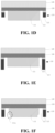
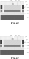
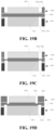
- FIGs. 1A-1F are structural diagrams showing a side sectional view of respective different variants of a first exemplary micro LED, according to some embodiments of the present disclosure.
- the micro LED includes a first type semiconductor layer 110, a light emitting layer 130, and a second type semiconductor layer 120.
- the light emitting layer 130 is formed on the first type semiconductor layer 110
- the second type semiconductor layer 120 is formed on the light emitting layer 130.
- the thickness of the first type semiconductor layer 110 is greater than the thickness of the second type semiconductor layer 120.
- a conductive type of the first type semiconductor layer 110 is different from a conductive type of the second type semiconductor layer 120.
- the conductive type of the first type semiconductor layer 110 is P type
- the conductive type of the second type semiconductor layer 120 is N type.
- the conductive type of the second type semiconductor layer 120 is P type
- the conductive type of the first type semiconductor layer 110 is N type.
- a material of the first type semiconductor layer 110 can be selected from one or more of p-GaAs, p-GaP, p-AlInP, p-GaN, p-InGaN, or p-AlGaN.
- the material of the second type semiconductor layer 120 can be selected from one or more of n-GaAs, n-AlInP, n-GaInP, n-AlGaAs, n-AlGaInP, n-GaN, n-InGaN, or n-AlGaN.
- the first type semiconductor layer 110 includes a mesa structure 111, a trench 112 and an ion implantation fence 113.
- the ion implantation fence 113 is separated from the mesa structure 111 by the trench 112.
- the trench 112 and the ion implantation fence 113 are annular around the mesa structure 111.
- the ion implantation fence 113 includes a light absorption material for absorbing light from the mesa structure 111.
- a conductive type of the light absorption material is the same as the conductive type of the first type semiconductor layer 110.
- the light absorption material is selected from one or more of p-GaAs, p-GaP, p-AlInP, p-GaN, p-InGaN, or p-AlGaN.
- the ion implantation fence 113 is formed at least by implanting ions into the first type semiconductor layer 110.
- ions implanted into the first type semiconductor layer 110 to form the ion implantation fence 113 are selected from one or more of H, N, Ar, Kr, Xe, As, O, C, P, B, Si, S, Cl, or F.
- the width of the ion implantation fence 113 is not greater than 50% of the diameter of the mesa structure 111. In some embodiments, the width of the ion implantation fence 113 is not greater than 10% of the diameter of the mesa structure 111. Preferably, the width of the ion implantation fence 113 is not greater than 200 nm, the diameter of the mesa structure 111 is not greater than 2500 nm, and the thickness of the first type semiconductor layer 110 is not greater than 300 nm.
- the width of the trench 112 is not greater than 50% of the diameter of the mesa structure 111. In some embodiments, the width of the ion implantation fence 113 is not greater than 10% of the diameter of the mesa structure 111. Preferably, the width of the trench 112 is not greater than 200 nm.
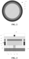
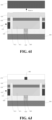
- FIG. 2 is a structural diagram showing a bottom view of the first exemplary micro LED shown in FIG. 1A , according to some embodiments of the present disclosure.
- FIG. 2 shows a bottom view of the first type semiconductor layer 110 in which the ion implantation fence 113 is separated from the mesa structure 111 by the trench.
- the ion implantation fence 113 is formed around the trench and the trench is formed around the mesa structure 111. Since the trench extends up through the first type semiconductor layer 110 and reaches the light emitting layer 130, the light emitting layer 130 can be seen through the trench in the bottom view.
- the trench 112 can extend up through the first type semiconductor layer 110, the emitting layer 130, even into the second type semiconductor layer 120.
- the trench 112 extends up through the first type semiconductor layer 110 and extends into the interior of the light emitting layer 130.
- the trench 112 can extend up through the first type semiconductor layer 110 and the light emitting layer 130.
- the trench 112 extends up through the first type semiconductor layer 110 and the light emitting layer 130, and further extends up into the interior of the second type semiconductor layer 120.
- the trench 112 can extend up through the first type semiconductor layer 110, the light emitting layer 130, and into the second type semiconductor layer 120.
- the top surface of the ion implantation fence 113 is lower than the top surface of the first type semiconductor layer 110.
- the ion implantation fence 113 cannot reach the light emitting layer 130.
- the top surface of the ion implantation fence 113 can be formed at any position within the first type semiconductor layer 110.
- the top surface of the ion implantation fence 113 is lower than the top surface of the trench 112.
- the bottom surface of the ion implantation fence 113 can be formed at any position, higher or lower than the bottom surface of the first type semiconductor layer 110.
- the bottom surface of the ion implantation fence 113 is aligned with the bottom surface of the first type semiconductor layer 110.
- the bottom surface of the ion implantation fence 113 is higher than the bottom surface of the first type semiconductor layer 110.
- the bottom surface of the ion implantation fence 113 is lower than the bottom surface of the first type semiconductor layer 110.
- the mesa structure 111 includes a stair structure 111a.
- the mesa structure 111 can have one or more stair structures.
- FIG. 3 is a structural diagram showing a side sectional view of another variant of the first exemplary micro LED, according to some embodiments of the present disclosure.
- the micro LED further includes a bottom isolation layer 140 filled in the trench 112.
- the material of the bottom isolation layer 140 is selected from one or more of SiO2, SiNx, Al2O3, AlN, HfO2, TiO2, or ZrO2.
- an integrated circuit (IC) backplane 190 is formed under the first type semiconductor layer 110 and is electrically connected with the first type semiconductor layer 110 via a connection structure 150.
- the connection structure 150 is a connection pillar.
- the micro LED further includes a bottom contact 160.
- the bottom contact 160 is formed at the bottom of the first type semiconductor layer 110.
- An upper surface of the connection structure 150 is connected with the bottom contact 160 and the bottom surface of the connection structure 150 is connected with the IC backplane 190. As shown in FIG. 3 , the bottom contact 160 protrudes from the first type semiconductor layer 110 as a bottom contact of the micro LED.
- the micro LED further includes a top contact 180 and a top conductive layer 170.
- the top contact 180 is formed on the top of the second type semiconductor layer 120.
- the top conductive layer 170 is formed on the top of the second type semiconductor layer 120 and the top contact 180.
- the conductive type of the top contact 180 is the same as the conductive type of the second type semiconductor layer 120
- the conductive type of the second type semiconductor layer 120 is N type and the conductive type of the top contact 180 is N type.
- the conductive type of the second type semiconductor layer 120 is P type and the conductive type of the top contact 180 is P type.
- the top contact 180 is made of metal or metal alloy, such as, AuGe, AuGeNi, etc.
- the top contact 180 is used for forming an ohmic contact between the top conductive layer 170 and the second type semiconductor layer 120, to optimize the electrical properties of the micro LED.
- the diameter of the top contact 180 is about 20-50 nm and the thickness of the top contact 180 is about 10 ⁇ 20nm.
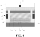
- FIG. 4 is a structural diagram showing a side sectional view of another variant of the first exemplary micro LED, according to some embodiments of the present disclosure.
- the connection structure 150 is a metal bonding layer for bonding the micro LED with the IC backplane 190.
- the bottom contact 160 is a bottom contact layer in this variant.
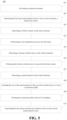
- FIG. 5 shows a flow chart of a method 500 for manufacturing the first exemplary micro LED, for example, the micro LED shown in FIG. 3 , according some embodiments of the present disclosure.
- the method 500 for manufacturing the micro LED includes steps 501-510.
- FIG. 6A to FIG. 6J are structural diagrams showing a side sectional view of the micro LED manufacturing process at each step (i.e., steps 501-510) corresponding to the method 500 shown in FIG. 5 , according to some embodiments of the present disclosure.
- an epitaxial structure is provided.
- the epitaxial structure includes a first type semiconductor layer 610, a light emitting layer 630, and a second type semiconductor layer 620 sequentially from top to bottom.
- the epitaxial structure is grown on a substrate 600.
- the substrate 600 can be GaN, GaAs, etc.
- step 502 referring to FIG. 6B , the first type semiconductor layer 610 is patterned to form a mesa structure 611, a trench 613 and a fence 613'.
- the first type semiconductor layer 610, the light emitting layer 630, and the second type semiconductor layer 620 are etched.
- the etching is stopped in the second type semiconductor layer 620. Therefore, the top surface of the trench 612 is within the second type semiconductor layer 620.
- the first type semiconductor layer 610 is etched and the etching is stopped on the light emitting layer 630, to avoid the light emitting layer 630 being etched in the patterning process. Referring back to FIG. 1A , the top of the trench 112 contacts the bottom surface of the light emitting layer 130, and the light emitting layer 130 is not etched in this variant.
- the step 502 further includes: etching the first type semiconductor layer and the light emitting layer in sequence, and stopping the etching in the light emitting layer.
- the top surface of the trench 112 can be at any position within the light emitting layer 130.
- the step 502 further includes: etching the first type semiconductor layer 610, the light emitting layer 630, and the second type semiconductor layer 620 in sequence, and stopping the etching in the second type semiconductor layer 620.
- the trench 112 extends up through the light emitting layer 130, and the top surface of the trench 121 can be at any position within the second type semiconductor layer 120.
- the first type semiconductor layer 610, the light emitting layer 630, and the second type semiconductor layer 620 are etched by a conventional dry etching process, such as, a plasma etching process, which can be understood be those skilled in the field.
- step 503 referring to FIG. 6C , a bottom contact 660 is deposited on the mesa structure 611.
- a first protective mask (not shown) is used to protect an area where the bottom contact 660 will not be formed. Then, the material of the bottom contact 660 is deposited on the first protective mask and on the first type semiconductor layer 610 by a conventional vapor deposition process, such as a physical vapor deposition process or a chemical vapor deposition process. After the deposition process, the first protective mask is removed from the first type semiconductor layer 610 and the material on the first protective mask is also removed with the first protective mask to form the bottom contact 660 on the mesa structure 611.
- step 504 referring to FIG. 6D , an ion implantation process is performed into the fence 613'.
- the arrows illustrate a direction of the ion implantation process.
- the ions are implanted into the fence 613' (as shown in FIG. 6C ) to form an ion implantation fence 613 (as shown in FIG. 6D ) by the ion implantation process, as shown in FIG. 6D .
- a second protective mask (not shown) is formed on an area in which no ions are to be implanted.
- the ions are implanted into the exposed fence 613'.
- the second protective mask is removed by a conventional chemical etching process, which can be understood by those skilled in the field.
- the implanting energy is 0 ⁇ 500Kev
- the implanting dose is 1E10-9E17.
- a bottom isolation layer 640 is deposited on the whole substrate 600. That is, the first type semiconductor layer 610 and the bottom contact 660 are covered by the bottom isolation layer 640, and the trench 612 is filled by the bottom isolation layer 640.
- the bottom isolation layer 640 is deposited by a conventional chemical vapor deposition process.
- the bottom isolation layer 640 is formed on sidewalls and a bottom surface of the trench 612. As shown in FIG. 6E , the bottom isolation layer 640 is filled into the trench 612. Therefore, the bottom isolation layer 640 is formed on the sidewalls of the first type semiconductor layer 610, the mesa structure 611, the light emitting layer 630, and the second type semiconductor layer 620 in the trench 612. In some embodiments, referring back to FIG. 1A , the bottom isolation layer is formed at the sidewalls of the mesa structure 111, the first type semiconductor layer 110, and the first ion implantation fence 113, and formed at a surface of the light emitting layer 130 in the first trench 112. In some embodiments, referring back to FIG. 1B , the bottom isolation layer is formed on the sidewalls of the mesa structure 111, the first type semiconductor layer 110 and the ion implantation fence 113, and the surface of the light emitting layer 130 in the trench 112.
- step 506 referring to FIG. 6F , the bottom isolation layer 640 is patterned to expose the bottom contact 660.
- the bottom isolation layer 640 is etched by a photo etching process and a dry etching process.
- a metal material 650' is deposited on the whole substrate 600. That is, the metal material 650'is deposited on the bottom isolation layer 640 and the bottom contact 660.
- the metal material is deposited by a conventional physical vapor deposition method.
- step 508 referring to FIG. 6H , the top of the metal material 650' is ground to the top of the bottom isolation layer 640, to form a connection structure 650 such as a connection pillar.
- the metal material is ground by a Chemical Mechanical Polishing (CMP) process.
- connection pillar 650 is bonded with an IC backplane 690.
- the epitaxial structure is firstly turned upside down.
- the connection pillar 650 is bonded with a contact pad of the IC backplane 690 by a metal bonding process.
- the substrate 600 is removed by a conventional separation method, such as, a laser stripping method, or a chemical etching method.
- the arrow illustrates a removal direction of the substrate 600.
- a top contact 680 and a top conductive layer 670 can be deposited in sequence on the second type semiconductor layer 620 by a conventional vapor deposition method.
- a micro LED array panel is further provided by some embodiments of the present disclosure.
- the micro LED array panel includes a plurality of micro LEDs as described above and shown in FIGs. 1A-1F , FIG. 3 and FIG. 4 . These micro LEDs can be arranged in an array in the micro LED array panel.
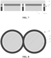
- FIG. 7 is a structural diagram showing a side sectional view of adjacent ones of the micro LED in FIG. 1C , in a micro LED panel, according to some embodiments of the present disclosure.
- the micro LED array panel includes a first type semiconductor layer 710, continuously formed in the micro LED array panel; a light emitting layer 730, continuously formed on the first type semiconductor layer 710; and a second type semiconductor layer 720, continuously formed on the light emitting layer 730.
- a conductive type of the first type semiconductor layer 710 is different from a conductive type of the second type semiconductor layer 720.
- the conductive type of the first type semiconductor layer 710 is P type
- the conductive type of the second type semiconductor layer 720 is N type.
- the conductive type of the second type semiconductor layer 720 is P type
- the conductive type of the first type semiconductor layer 710 is N type.
- the thickness of the first type semiconductor layer 710 is greater than the thickness of the second type semiconductor layer 720.
- the material of the first type semiconductor layer 710 is selected from one or more of p-GaAs, p-GaP, p-AlInP, p-GaN, p-InGaN, or p-AlGaN.
- the material of the second type semiconductor layer 720 is selected from one or more of n-GaAs, n-AlInP, n-GaInP, n-AlGaAs, n-AlGaInP, n-GaN, n-InGaN, or n-AlGaN.
- the first type semiconductor layer 710 includes multiple mesa structures 711, multiple trenches 712, and multiple ion implantation fences 713 separated from the mesa structures 711 by the trenches 712.
- the top surface of the ion implantation fence 713 is lower than the top surface of the first type semiconductor layer 710. Thus, the top surface of the trench 712 does not contact to the light emitting layer 730.
- the relationship of the top surface of the ion implantation fence 713, the top surface of the first type semiconductor layer 710, the top surface of the trench 712 can be seen in the micro LED shown in FIGs. 1B-1D , the description of which will not be further described here.
- the mesa structure can have one or multiple stair structures in another embodiment as seen in the mesa structure shown in FIG. 1F .
- FIG. 8 is a structural diagram showing a bottom view of the adjacent micro LEDs in FIG. 7 , according to some embodiments of the present disclosure.
- the ion implantation fences 713 are formed around in the trench 712 and between the adjacent mesa structures 711. Furthermore, in each micro LED, the ion implantation fence 713 is formed around the trench 712 and the trench 712 is formed around the mesa structure 711. The electrical resistance of the ion implantation fence 713 is higher than the electrical resistance of the mesa structure 711.
- the space between the adjacent sidewalls of the adjacent ones of the mesa structure 711 can be adjusted.
- the space between the adjacent sidewalls of the mesa structures 711 is not greater than 50% of the diameter of the mesa structure 711.
- the space between the adjacent sidewalls of the mesa structures 711 is not greater than 30% of the diameter of the mesa structure 711.
- the space between the adjacent sidewalls of the mesa structure 711 is not greater than 600 nm.
- the width of the ion implantation fence 713 can be adjusted.
- the width of the ion implantation fence 713 can be not greater than 50% of the diameter of the mesa structure 711.
- the width of the ion implantation fence 713 can be not greater than 10% of the diameter of the mesa structure 711.
- the width of the ion implantation fence 713 is not greater than 200 nm.
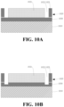
- FIG. 9 is a structural diagram showing a side sectional view of adjacent ones of the micro LED in FIG. 3 , in a micro LED array panel, according to some embodiments of the present disclosure.
- the micro LED array panel further includes a bottom isolation layer 940 formed on a first type semiconductor layer 910 and filled in a trench 912.
- the material of the bottom isolation layer 940 is one or more of SiO2, SiNx, or Al2O3, AlN, HfO2, TiO2, or ZrO2.
- an IC backplane 990 is continuously formed under the first type semiconductor layer 910 and is electrically connected with the first type semiconductor layer 910 via a connection structure 950.
- the micro LED array panel further includes a bottom contact 960 formed at the bottom of the first type semiconductor layer 910. Further detail of the bottom isolation layer 940, the IC backplane 990, the bottom contact 960 and the connection structure 950 are shown in the micro LED in FIGs. 3 and 4 , respectively as corresponding to the bottom isolation layer 140, the IC backplane 190, the bottom contact 160, and the connection structure 150, which will not be further described.
- the micro LED array panel further includes a top contact 980 and a top conductive layer 970.
- the top contact 980 is formed on the top of a second type semiconductor layer 920.
- the top conductive layer 970 is formed on the top of the second type semiconductor layer 920 and the top contact 980.
- a conductive type of the top contact 980 is the same as a conductive type of the second type semiconductor layer 920.
- the conductive type of the second type semiconductor layer 920 is N type and the conductive type of the top contact 980 is N type.
- the conductive type of the second type semiconductor layer 920 is P type and the conductive type of the top contact 980 is P type.
- the top contact 980 is made of metal or metal alloy, such as, AuGe, AuGeNi, etc.
- the top contact 980 is used for forming ohmic contact between the top conductive layer 970 and the second type semiconductor layer 920, to optimize the electrical properties of the micro LEDs.
- the diameter of the top contact 980 is about 20-50 nm and the thickness of the top contact 980 is about 10 ⁇ 20nm.
- the micro LED array panel can be manufactured by the method 500 as shown in FIG. 5 , which will not be further described .
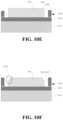
- FIGs. 10A -10F are structural diagrams showing a side sectional view of respective different variants of a second exemplary micro LED, according to some embodiments of the present disclosure.
- the micro LED includes a first type semiconductor layer 1010, a light emitting layer 1030 and a second type semiconductor layer 1020.
- a conductive type of the first type semiconductor 1010 is different from a conductive type of the second type semiconductor layer 1020.
- the conductive type of the first type semiconductor 1010 is P type and the conductive type of the second type semiconductor layer 1020 is N type.
- the second type semiconductor layer 1020 includes a mesa structure 1021, a trench 1022, and an ion implantation fence 1023 separated from the mesa structure 1021.
- the bottom surface of the ion implantation fence 1023 is higher than the bottom surface of the second type semiconductor layer 1020. Furthermore, the ion implantation fence 1023 is formed around the trench 1022 and the trench 1022 is formed around the mesa structure 1021.
- the electrical resistance of the ion implantation fence 1023 is higher than the electrical resistance of the mesa structure 1021.
- the ion implantation fence 1023 includes a light absorption material for absorbing light from the mesa structure 1021.
- a conductive type of the light absorption material is the same as the conductive type of the second type semiconductor layer 1020.
- the light absorption material is selected from one or more of n-GaAs, n-GaP, n-AlInP, n-GaN, n-InGaN, or p-AlGaN.
- the ion implantation fence 1023 is formed at least by implanting ions into the second type semiconductor layer 1020.
- the ion type implanted into the second type semiconductor layer 1020 is selected from one or more of H, N, Ar, Kr, Xe, As, O, C, P, B, Si, S, Cl, or F.
- the width of the ion implantation fence 1023 is not greater than 50% of the diameter of the mesa structure 1021. In some embodiments, the width of the ion implantation fence 1023 is not greater than 10% of the diameter of the mesa structure 1021. Preferably, the width of the ion implantation fence 1023 is not greater than 200 nm. The diameter of the mesa structure 1021 is not greater than 2500 nm. The thickness of the second type semiconductor layer 1020 is not greater than 100 nm.
- the width of the trench 1022 is not greater than 50% of the diameter of the mesa structure 1021. In some embodiments, the width of the trench 1022 is not greater than 10% of the diameter of the mesa structure 1021. Preferably, the width of the second trench 1022 is not greater than 200 nm.
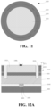
- FIG. 11 is a structural diagram showing a top view of the second exemplary micro LED shown in FIG. 10A , according to some embodiments of the present disclosure.
- FIG. 11 shows a top view of the second type semiconductor layer 1020 in which the ion implantation fence 1023 is separated from the mesa structure 1021 by the trench 1022.
- FIG. 11 shows the light emitting layer 1030 at the bottom of the trench 1022.
- the ion implantation fence 1023 is formed around the trench 1022 and the trench 1022 is formed around the mesa structure 1021.
- the trench 1022 can extend down through the bottom surface of the second type semiconductor layer 1020 but cannot reach the light emitting layer 1030. In some embodiments, the trench 1022 can extend down through the second type semiconductor layer 1020 and can reach the light emitting layer 1030. In some embodiments, the trench 1022 can extend down through the second type semiconductor layer 1020 and extend into the interior of the light emitting layer 1030. In some embodiments, the trench 1022 can extend down through the second type semiconductor layer 1020 and the light emitting layer 1030. Furthermore, the trench 1022 can extend down through the second type semiconductor layer 1020 and the light emitting layer 1030, and extend down into the interior of the first type semiconductor layer 1010.
- the trench 1022 extends down through the bottom surface of the second type semiconductor layer 1020 and reaches the light emitting layer 1030.
- the bottom surface of the trench 1022 is aligned with the bottom of the second type semiconductor layer 1020.
- the bottom surface of the trench 1022 exposes the light emitting layer 1030.
- the trench 1022 extends down through the second type semiconductor layer 1020 and extends into the interior of the light emitting layer 1030. In some embodiments, as shown in FIG. 10C , the trench 1022 extends down through the second type semiconductor layer 1020, the light emitting layer 1030, and extends down into the interior of the first type semiconductor layer 1010.
- the bottom surface of the ion implantation fence 1023 is higher than the bottom surface of the trench 1022.
- the bottom surface of the ion implantation fence 1023 can be formed at any position within the first type semiconductor layer 1010.
- the top surface of the ion implantation fence 1023 can be formed at any position. Preferably, the top surface of the ion implantation fence 1023 is aligned with the top surface of the second type semiconductor layer 1020. In some embodiments, as shown in FIG. 10D , the top surface of the ion implantation fence 1023 is higher than the top surface of the second type semiconductor layer 1020. In some embodiments, as shown in FIG. 10E , the top surface of the ion implantation fence 1023 is lower than the top surface of the second type semiconductor layer 1020.
- the mesa structure 1021 includes one stair structure 1021a. In some embodiments, the mesa structure 1021 can have multiple stair structures.
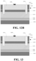
- FIGs. 12A and 12B are structural diagram showing a side sectional view of other variants of the second exemplary micro LED, according to some embodiments of the present disclosure.
- the micro LED further includes a bottom isolation layer 1040 formed under the first type semiconductor layer 1010.
- a material of the bottom isolation layer 1040 is selected from one or more of SiO2, SiNx, or Al2O3.
- an integrated circuit (IC) backplane 1090 is formed under the first type semiconductor layer 1010 and is electrically connected with the first type semiconductor layer 1010 via a connection structure 1050.
- the connection structure 1050 is a connection pillar.
- the micro LED further includes a bottom contact 1060 formed at the bottom of the first type semiconductor layer 1010.
- An upper surface of the connection structure 1050 is connected with the bottom contact 1060 and the bottom of the connection structure 1050 is connected with the IC backplane 1090.
- the bottom contact 1060 protrudes from the first type semiconductor layer 1010 as a bottom contact of the micro LED.
- the micro LED further includes a top contact 1080 and a top conductive layer 1070.
- the top contact 1080 is formed on the top of the second type semiconductor layer 1020.
- the top conductive layer 1070 is formed on the top surface of the second type semiconductor layer 1020 and the top surface of the top contact 1080, and covers sidewalls and the bottom of the trench 1022.
- a dielectric layer 1071 is formed on the sidewalls and bottom surface of the trench 1022.
- a conductive type of the top contact 1080 is the same as a conductive type of the second type semiconductor layer 1020.
- the conductive type of the second type semiconductor layer 1020 is N type and the conductive type of the top contact 1080 is N type.
- the top contact 1080 is made of metal or metal alloy, such as, AuGe, AuGeNi, etc.
- the top contact 1080 is used for forming an ohmic contact between the top conductive layer 1070 and the second type semiconductor layer 1020, to optimize the electrical properties of the micro LED.
- the diameter of the top contact 1080 is about 20-50 nm and the thickness of the top contact 1080 is about 10 ⁇ 20nm.
- connection structure 1050 can be a metal bonding layer for bonding the micro LED with the IC backplane 1090.
- the bottom contact 1060 is a bottom contact layer in this embodiment.
- FIG. 13 is a structural diagram showing a side sectional view of another variant of the second exemplary micro LED, according to some embodiments of the present disclosure.
- the dielectric layer 1071 fills the second trench 1022.
- the top conductive layer 1070 is formed on the top of the second type semiconductor layer 1020, the top of the top contact 1080, and the top surface of the dielectric layer 1071.
- the dielectric layer 1071 can be formed on the top surface of second type semiconductor layer.
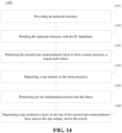
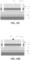
- FIG. 14 shows a flow chart of a method 1400 for manufacturing the second exemplary micro LED, for example the micro LED shown in FIG. 12B , according some embodiments of the present disclosure.
- the method for manufacturing the micro LED includes steps 1401-1406.
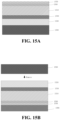
- FIGs. 15A-15F are structural diagrams showing a side sectional view of a micro LED manufacturing process in each step (i.e., steps 1401 to 1406) of the method 1400 shown in FIG. 14 , according to some embodiments of the present disclosure.
- an epitaxial structure is provided.
- the epitaxial structure includes a first type semiconductor layer 1510, a light emitting layer 1530 and a second type semiconductor layer 1520 sequentially from top to bottom.
- the epitaxial structure is grown on a substrate 1500.
- the substrate 1500 can be GaN, GaAs, etc.
- a bottom contact layer 1560 used as the bottom contact is deposited on the top surface of the first type semiconductor layer 1510. Then, a metal bonding layer which is used as a connection structure 1550 is deposited on the top surface of the bottom contact layer 1560.
- step 1402 referring to FIG. 15B , the epitaxial structure is bonded with an IC backplane 1590.
- the epitaxial structure is firstly turned upside down.
- the connection structure 1550 is bonded with a contact pad of the IC backplane 1590 by a metal bonding process.
- the substrate 1500 is removed by a conventional separation method, such as, a laser stripping method, or a chemical etching method.
- the arrow illustrates a removal direction of the substrate 1500.
- step 1403 referring to FIG. 15C , the second type semiconductor layer 1520 is patterned to form a mesa structure 1521, a trench 1522 and a fence 1523'.
- the second type semiconductor layer 1520 is etched down to the surface of the light emitting layer 1530, to avoid the light emitting layer 1530 being etched in the patterning process. For example, referring back to FIG. 10A , the bottom surface of the trench 1022 exposes the light emitting layer 1030.
- step 1403 further includes: etching the second type semiconductor layer 1520 and the light emitting layer 1530 in sequence, and stopping the etching process in the light emitting layer 1530. For example, referring back to FIG. 10B , the bottom of the trench 1022 contacts the light emitting layer 1030, and is provided within the light emitting layer 1030.
- step 1403 further includes: etching the second type semiconductor layer, the light emitting layer, and the first type semiconductor layer 1510 in sequence, and stopping the etching process in the first type semiconductor layer. Referring back to FIG. 15C , the bottom of the trench 1522 contacts the first type semiconductor layer 1510, and is provided within the first type semiconductor layer 1510.
- the second type semiconductor layer 1520 is etched by a conventional dry etching process, such as, a plasma etching process, which can be understood be those skilled in the field.
- a top contact 1580 is deposited on the mesa structure 1521.
- a first protective mask (not shown) is used to protect an area where the top contact 1580 will not be formed.
- the material of the top contact 1580 is deposited on the first protective mask and on the second type semiconductor layer 1520 by a conventional vapor deposition process, such as a physical vapor deposition process or a chemical vapor deposition process.
- the first protective mask is removed from the second type semiconductor layer 1520 and the material on the first protective mask is also removed with the first protective mask to form a top contact 1580 on the mesa structure 1521.
- step 1405 referring to FIG. 15E , an ion implantation process is performed into the fence 1523'.
- the ions are implanted into the fence 1523' (as shown in FIG. 15D ) to form an ion implantation fence 1523 (as shown in FIG. 15E ) by an ion implantation process.
- the arrows in FIG. 15E illustrate a direction of the ion implantation process.
- a second protective mask (not shown) is formed on the area in which no ions are to be implanted.
- the ions are implanted into the exposed fence 1523' (as shown in FIG. 15D ).
- the second protective mask is removed by a conventional chemical etching process, which can be understood by those skilled in the field.
- the implanting energy is 0 ⁇ 500Kev
- the implanting dose is 1E10-9E17.
- the top contact 1580 can be formed after the ion implantation process.
- a top conductive layer 1570 is deposited on the top of the second type semiconductor layer 1520 and on the top contact 1580, and covers the sidewalls and the bottom of the trench 1522.
- the top conductive layer 1570 is deposited by a conventional physical vapor deposition process.
- a dielectric layer can be formed on the sidewalls and the bottom of the trench 1522 before depositing the top conductive layer 1570. More particularly, before forming the top conductive layer 1570, a dielectric layer 1571 is formed on the sidewall and the bottom of the trench 1522. Furthermore, the dielectric layer 1571 is formed on the sidewalls of the first type semiconductor layer 1510, the light emitting layer 1530 and the mesa structure 1521 in the trench 1522. The top conductive layer 1570 is formed on the surface of the dielectric layer 1571 extending into the trench 1522, on the top of the mesa structure 1521, and the top of the ion implantation fence 1523. Referring back to FIG.
- the dielectric layer 1071 can fully fill in the trench 1022.
- the dielectric layer can be formed on the sidewall of the second type semiconductor layer 1020, the mesa structure 1021 in the trench 1022 and on the surface of the light emitting layer 1030 in the trench 1022.
- the dielectric layer can be formed on the sidewall of the second type semiconductor layer 1020 and the mesa structure 1021 in the trench 1022 and on the surface of the light emitting layer 1030 in the trench 1022.
- a micro lens can be further formed on the top conductive layer 1570, which can be understood by those skilled in the field.
- step 1402 can be replaced with the following step 1402': depositing a bottom contact on the first type semiconductor layer; depositing a bottom isolation layer on the whole substrate; patterning the bottom isolation layer to expose the bottom contact; depositing metal material on the whole substrate; grinding the top of the metal material to the top of the bottom isolation layer, to form a connection pillar; and bonding the connection pillar with an IC backplane.
- the epitaxial structure is turned upside down, and the connection pillar is bonded with a contact pad of the IC backplane by a metal bonding process.
- Step 1402' can further understood by also referring to the description of FIG. 6C and FIGs. 6E -6I in the embodiment 1, which will not be further described here.
- a micro LED array panel is further provided according to some embodiments of the present disclosure.
- the micro LED array panel includes a plurality of micro LEDs as described above with reference to FIGs. 10A-10F , FIG. 12A and 12B . These micro LEDs can be arranged in an array in the micro LED array panel.
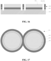
- FIG. 16 is a structural diagram showing a side sectional view of adjacent ones of the micro LED in FIG. 10C , in a micro LED panel, according to some embodiments of the present disclosure.
- the micro LED array panel includes a first type semiconductor layer 1610, continuously formed in the micro LED array panel; a light emitting layer 1630, continuously formed on the first type semiconductor layer 1610; and a second type semiconductor layer 1620, continuously formed on the light emitting layer 1630.
- the second type semiconductor layer 1620 includes multiple mesa structures 1621, multiple trenches 1622, and multiple ion implantation fences 1623 separated from the mesa structures 1621 by the trenches 1622.
- the bottom surface of the ion implantation fence 1623 is higher than the bottom surface of the second type semiconductor layer 1620.
- FIG. 17 is a structural diagram showing a top view of the adjacent micro LEDs in FIG. 16 , according to some embodiments of the present disclosure.
- FIG. 17 shows a top view of the second type semiconductor layer 1620 in which the ion implantation fences 1623 are formed around the trench 1622 and between the adjacent mesa structures 1621.
- the electrical resistance of the ion implantation fence 1623 is higher than the electrical resistance of the mesa structure 1621.
- the ion implantation fence 1623 is formed around the trench 1622 and the trench 1622 is formed around the mesa structure 1621.
- the trench 1622 can extend down through the second type semiconductor layer 1620 and the light emitting layer 1630, and extend down into the interior of the first type semiconductor layer 1610. In some embodiments, referring back to FIG. 10A , the trench 1022 extends down through the second type semiconductor layer 1020 and reaches the light emitting layer 1030. In some embodiments, referring back to FIG. 10B , the trench 1022 extends down through the second type semiconductor layer 1020, and extends into the interior of the light emitting layer 1030.
- Variations in the relationship of the bottom surface of the ion implantation fence 1623, and the bottom surface of the second type semiconductor layer 1620, and the bottom of the trench 1622 can generally correspond to those shown for the micro LEDs in FIGs. 10A-10C , which will not be further described here. Additionally, in some embodiments, variations in the relationship of the top surface of the ion implantation fence 1623 and the top surface of the second type semiconductor layer 1620 can generally correspond to those shown for the micro LEDs in FIGs. 10C-10E , which will not be further described here. In some embodiments, the mesa structure can have one or multiple stair structures as shown in FIG. 10F .
- the space between the adjacent sidewalls of adjacent ones of the mesa structures 1621 can be adjusted.
- the space between the adjacent sidewalls of the mesa structures 1621 is not greater than 50% of the diameter of the mesa structure 1621.
- the space between the adjacent sidewalls of the mesa structures 1621 is not greater than 30% of the diameter of the mesa structure 1621.
- the space between the adjacent sidewalls of the mesa structures 1621 is not greater than 600 nm.
- the width of the ion implantation fence 1623 can be adjusted.
- the width of the ion implantation fence 1623 is not greater than 50% of the diameter of the mesa structure 1621. In some embodiments, the width of the ion implantation fence 1623 is not greater than 10% of the diameter of the mesa structure 1621. Preferably, in the micro LED array panel, the width of the ion implantation fence 1623 is not greater than 200 nm.
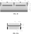
- FIG. 18 is a structural diagram showing a side sectional view of adjacent ones of the micro LED in FIG. 12B , in a micro LED array panel, according to some embodiments of the present disclosure.
- the micro LED array panel further includes a top contact 1880 and a top conductive layer 1870. Further details of the top contact 1880 and the top conductive layer 1870 can be understood by also referring to the micro LEDs shown in FIGs. 10A-10F , FIG. 12 and FIG. 13 , which will not be further described here.
- an IC backplane 1890 is formed under a first type semiconductor layer 1810 and is electrically connected with the first type semiconductor layer 1810 via a connection structure 1850.
- the micro LED array panel further includes a bottom contact 1860 formed at the bottom of the first type semiconductor layer 1810.
- the connection structure 1850 can be a metal bonding layer for bonding the micro LED with the IC backplane 1890.
- the bottom contact 1860 is a bottom contact layer. Further details of the IC backplane 1890, the bottom contact 1860 and the connection structure 1850 can be understood by also referring to FIGs. 12A , 12B and 13 , which will not be further described here.
- micro LEDs and the ion implantation fence in the micro LED array panel can be understood by also referring to the micro LEDs as shown in FIGs. 10A-10F , which will not be further described here.
- the micro LED array panel shown in FIG. 18 can be manufactured by the method 1400 of manufacturing the micro LED as shown in FIG. 14 , which will not be further described here.
- FIGs. 19A-19E are structural diagram showing a side sectional view of respective different variants of a third exemplary micro LED, according to some embodiments of the present disclosure.
- the micro LED at least includes a first type semiconductor layer 1910, a light emitting layer 1930, and a second type semiconductor layer 1920.
- a conductive type of the first type semiconductor layer 1910 is different from a conductive type of the second type semiconductor layer 1920.
- the conductive type of the first type semiconductor layer 1910 is P type and the conductive type of the second type semiconductor layer 1920 is N type.
- the conductive type of the second type semiconductor layer 1920 is P type and the conductive type of the first type semiconductor layer 1910 is N type.
- the thickness of the first type semiconductor layer 1910 is greater than the thickness of the second type semiconductor layer 1920.
- a material of the first type semiconductor layer 1910 is selected from one or more of p-GaAs, p-GaP, p-AlInP, p-GaN, p-InGaN, or p-AlGaN
- a material of the second type semiconductor layer 1920 is selected from one or more of n-GaAs, n-AlInP, n-GaInP, n-AlGaAs, n-AlGaInP, n-GaN, n-InGaN, or n-AlGaN.
- the first type semiconductor layer 1910 includes a first mesa structure 1911, a first trench 1912 and a first ion implantation fence 1913.
- the first trench 1912 extends up through the top surface of the first type semiconductor layer 1910.
- the second type semiconductor layer 1920 includes a second mesa structure 1921, a second trench 1922 and a second ion implantation fence 1923 separated from the second mesa structure 1921.
- the first trench extends up through the first type semiconductor layer and contacts the light emitting layer.
- the first trench extends up through the first type semiconductor layer and extends into the interior of the light emitting layer.
- the first trench extends up through the first type semiconductor layer and the light emitting layer, and extends up into the interior of the second type semiconductor layer. Additionally, the first trench can extend up through the first type semiconductor layer and the light emitting layer, and the second type semiconductor layer.
- the second trench 1922 extends down through the bottom of the second type semiconductor layer 1920 and the bottom of the second trench 1922 is lower than the bottom of the second type semiconductor layer 1920. Thus, the bottom of the second trench 1922 contacts to the light emitting layer 1930.
- the second trench extends down to the bottom of the second type semiconductor layer and contacts the light emitting layer.
- the second trench extends down through the second type semiconductor layer and extends into the interior of the light emitting layer.
- the second trench extends down through the second type semiconductor layer and the light emitting layer, and further extends down into the interior of the first type semiconductor layer. Additionally, in some embodiments, the second trench can extend down through the second type semiconductor layer, the light emitting layer, and the first type semiconductor layer.
- the top surface of the first trench 1912 does not touch the bottom surface of the second trench 1922, in either the horizontal direction or the vertical direction. Part of the light emitting layer 1930 is disposed between the top surface of the first trench 1912 and the bottom surface of the second trench 1922. Additionally, in some embodiments, referring to FIGs. 19E and 19F , the top of the first trench 1912 is directly connected with the bottom of the second trench 1922, in the horizontal direction or in the vertical direction. Therefore, there is no light emitting layer 1930 between the top of the first trench 1911 and the bottom of the second trench 1922. For example, as shown in FIG.
- the first trench 1912 and the second trench 1922 can be as one trench structure when the first trench 1912 and the second trench 1922 extend through to each other in the vertical direction.
- the center of the first trench 1912 can be aligned with or shifted from the center of the second trench 1922.
- the first trench 1912 and the second trench 1022 do not align with each other in vertical direction.
- the diameter of the first trench 1912 from top down can be the same or different.
- the diameter of the second trench 1922 from upside down can be the same or different.
- the diameter of the first trench 1912 can be the same as or different from the diameter of the second trench 1922.
- the center of the first mesa structure 1911 is aligned with the center of the second mesa structure 1921.
- the center of the first trench 1912 is aligned with the center of the second trench 1922, and the center of the first ion implantation fence 1913 is aligned with the center of the second ion implantation fence 1923.
- a bottom view of the first type semiconductor layer 1910 is similar to the bottom view shown in FIG. 2 .
- the first ion implantation fence 1913 is separated from the first mesa structure 1911 by the first trench 1912.
- the first ion implantation fence 1913 is formed around the first trench 1912 and the first trench 1912 is formed around the first mesa structure 1911.
- a top view of the second type semiconductor layer 1920 is similar to the top view shown in FIG. 11 in that the second ion implantation fence 1923 is separated from the second mesa structure 1921 by the second trench 1922.
- the second ion implantation fence 1923 is formed around the second trench 1922 and the second trench 1922 is formed around the second mesa structure 1921.
- the first mesa structure 1911 can have one or multiple stair structures, as shown in FIG. 1F .
- the second mesa structure 1921 can have one or multiple stair structures, as shown in FIG. 10F .
- FIG. 20 is a structural diagram showing a side sectional view of another variant of the third exemplary micro LED, according to some embodiments of the present disclosure.
- the micro LED further includes a bottom isolation layer 2040 filled in a first trench 2012.
- the material of the bottom isolation layer 2040 is one or more of SiO2, SiNx, or Al2O3.
- An IC backplane 2090 is formed under a first type semiconductor layer 2010 and is electrically connected with the first type semiconductor layer 2010 via a connection structure 2050.
- the connection structure 2050 is a connection pillar.
- the micro LED further includes a bottom contact 2060 formed at the bottom of the first type semiconductor layer 2010. Further detail of the bottom isolation layer 2040, the IC backplane 2090, the connection structure 2050, and the bottom contact 2060 can be found by referring to the description of Embodiment 1, which will not be further described here.
- the micro LED further includes a top contact 2080 and a top conductive layer 2070.
- the top contact 2080 is formed on the top of a second type semiconductor layer 2020 and the top conductive layer 2070 is formed on the top of the second type semiconductor layer 2020.
- the top conductive layer 2070 covers the top contact 2080 and covers the sidewalls of the second trench 2022. Further detail regarding the top contact 2080 and the top conductive layer 2070 can be found by referring to the description of Embodiment 2, which will not be further described here.
- micro LED the first ion implantation fence 2013, and the second ion implantation fence 2023 can be found by referring to description of Embodiment 1 and Embodiment 2, which will not be further described here.
- FIG. 21 shows a flow chart of a method 2100 for manufacturing the third exemplary micro LED, according some embodiments of the present disclosure.
- the method 2100 includes at least Process I and Process II.
- Process I the first type semiconductor layer is patterned, and then ions are implanted into the first type semiconductor layer, to form a first ion implantation fence.
- the second type semiconductor layer is patterned, and then ions are implanted into the second type semiconductor layer, to form a second ion implantation fence.
- the Process I at least includes steps 2101-2109, and the Process II at least includes steps 2110-2113.
- steps 2101-2109 are similar to the steps 501-509 of method 500, respectively, as shown in FIG. 5 .
- the side sectional views for the micro LED being manufactured according to steps 2101-2109 are similar to the views shown in FIGs. 6A-6I , respectively.
- step 2101 referring to FIG. 6A , an epitaxial structure is provided.
- step 2102 referring to FIG. 6B , the first type semiconductor layer 610 is patterned to form the mesa structure 611, the trench 612 and the fence 613'.
- step 2103 referring to FIG. 6C , the bottom contact 660 is deposited on the mesa structure 611.
- step 2104 referring to FIG. 6D , an ion implantation process is performed into the fence 613'.
- step 2105 referring to FIG. 6E , the bottom isolation layer 640 is deposited on the whole substrate 600.
- the bottom isolation layer 2040 fills the first trench 2012. Furthermore, when the first trench 2012 extends through the first type semiconductor layer 2010 and the light emitting layer 2030, and extends into the second type semiconductor layer 2020, the bottom isolation layer 2040 is further formed on the sidewalls of the first mesa structure 2011, the first ion implantation fence 2013, the first type semiconductor layer 2010, the light emitting layer 2030, the second type semiconductor layer 2020, the second mesa structure 2021, and the second ion implantation fence 2023 in the first trench 2012.
- step 2106 referring to FIG. 6F , the bottom isolation layer 640 is patterned to expose the bottom contact 660.
- step 2107 referring to FIG. 6G , metal material 650' is deposited on the whole substrate 600.
- step 2108 referring to FIG. 6H , the top of the metal material 650' is ground to the top of the isolation layer 640, to form a connection pillar 650.
- step 2109 referring to FIG. 6I , the connection pillar 650 is bonded with the IC backplane 690, and the substructure 600 is removed.
- FIGs. 22A-22D are structural diagrams showing a side sectional view of the micro LED manufacturing process at steps 2110-2113 of the method 2100 shown in FIG. 21 , according to some embodiments of the present disclosure.
- a second type semiconductor layer 2220 is patterned to form a second mesa structure 2221, a second trench 2222 and a second fence 2223.
- the center axis of the second trench 2222 is aligned with the center axis of a first trench 2212.
- the center axis of the second trench 2222 is not aligned with the center axis of the first trench 2212.
- the second trench 2222 is etched to be connected with the first trench 2212. That is, the second trench 2222 is etched to the surface of the bottom isolation layer 2240 filled in the first trench 2212.
- step 2111 referring to FIG. 22B , a top contact 2280 is deposited on the mesa structure 2221.
- step 2112 referring to FIG. 22C , an ion implantation process is performed into the fence 2223'.
- the arrows illustrate a direction of the ion implantation process.
- a top conductive layer 2270 is deposited on the top of the second type semiconductor layer 2220 and on the top contact 2280, and on the sidewalls of the trench 2222.
- the top conductive layer 2270 can be directly formed on the top of the second type semiconductor layer 2220 and on the top contact 2280, and on the sidewalls of the trench 2222.
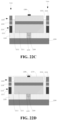
- FIGs. 23A and 23B are structural diagram showing a side sectional view of other variants of a third exemplary micro LED, according to some embodiments of the present disclosure.
- a bottom isolation layer 2340 is filled in a first trench 2312, and formed on the sidewall of the first mesa structure 2311, the first ion implantation fence 2313, and the light emitting layer 2330 in the first trench 2312.
- a dielectric layer 2371 is deposited extending into a second trench 2322.
- the side wall dielectric layer 2371 is formed on the sidewall and the bottom of the second trench 2322.
- the second trench 2322 extends down through the second type semiconductor layer 2320 and into the light emitting layer 2330.
- the dielectric layer 2371 is formed on the sidewall of the second mesa structure 2321, the second type semiconductor layer 2320, the second ion implantation fence 2323, and the light emitting layer 2330 in the second trench 2322. Then the top conductive layer 2370 is formed on the surface of the dielectric layer 2371 extending into the second trench 2322, and formed on the top of the second mesa structure 2321 and the top of second ion implantation fence 2323.
- the bottom isolation layer 2340 is filled in the first trench 2312, and formed on the sidewall of the first mesa structure 2311, the first ion implantation fence 2313 and the first type semiconductor layer 2310.
- the top conductive layer 2370 can be formed extending into the second trench 2322.
- the dielectric layer 2371 is formed extending into the second trench 2322.
- the second trench 2322 extends down through the second type semiconductor layer 2320, the light emitting layer 2330, and into the first type semiconductor layer 2310.
- the dielectric layer 2371 is formed on the sidewall of the second mesa structure 2321, the second type semiconductor layer 2320, the second ion implantation fence 2323, the light emitting layer 2330, the first mesa structure 2311, the first ion implantation fence 2313 and the first type semiconductor layer 2310 in the second trench 2322.
- the bottom isolation layer 2340 is formed on the sidewalls and the top of the first trench 2312
- the dielectric layer 2371 is formed on the sidewalls and the bottom of the second trench 2322.
- the thickness of the bottom isolation layer extending into the first trench 2312 depends on a position of the bottom of the second trench 2322 and a position of the top of the first trench 2312.
- the thickness of the dielectric layer 2371 extending into the second trench 2322 depends on a position of the bottom of the second trench 2322 and a position of the top of the first trench 2312.
- the top contact and the bottom contact can be formed in the micro LED according to some embodiments of the present disclosure, which will not be further described here.
- a micro LED array panel is further provided according to some embodiments of the present disclosure.
- the micro LED array panel includes a plurality of micro LEDs as described above and shown in FIGs. 19A-19E , FIG. 20 and FIGs. 23A and 23B. These micro LEDs can be arranged in an array in the micro LED array panel.
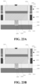
- FIG. 24 is a structural diagram showing a side sectional view of adjacent ones of the micro LED in FIG. 23A , in a micro LED array panel, according to some embodiments of the present disclosure.
- the micro LED array panel at least includes a first type semiconductor layer 2410 continuously formed in the micro LED array panel; a light emitting layer 2430 continuously formed on the first type semiconductor layer 2410; and a second type semiconductor layer 2420 formed on the light emitting layer 2330.
- the first type semiconductor layer 2410 includes multiple first mesa structures 2311, multiple first trenches 2412 and multiple first ion implantation fences 2413 separated from the first mesa structures via the first trenches 2412.
- the top surface of the first ion implantation fence 2413 is lower than the top surface of the first type semiconductor layer 2410.
- a bottom view of the micro LED array panel without an IC backplane is similar to the bottom view shown in FIG. 8 .
- the first ion implantation fences 2413 are formed around the first trench 2412 between the adjacent first type mesa structures 2411.
- the electrical resistance of the first ion implantation fence 2413 is higher than the electrical resistance of the first mesa structure.
- the first ion implantation fence 2313 is formed around the first trench 2412 and the first trench 2412 is formed around the first mesa structure.
- the second type semiconductor layer 2420 includes multiple second mesa structures 2421, multiple second trenches 2422 and multiple second ion implantation fences 2423 separated from the second mesa structures 2421 by the second trenches 2422.
- the bottom surface of the second ion implantation fence 2423 is higher than the bottom surface of the second type semiconductor layer 2420.
- a top view of the micro LED array panel is similar to the top view shown in FIG. 17 in that the second ion implantation fences 2423 being formed around the second trench 2422 between the adjacent second mesa structures 2421.
- the electrical resistance of the second ion implantation fence 2423 is higher than the electrical resistance of the second mesa structure 2421.
- the second ion implantation fence 2323 is formed around the second trench 2422 and the second trench 2422 is formed around the second mesa structure 2421.
- the space between the adjacent sidewalls of the first mesa structures 2411 can be adjusted.
- the space between the adjacent sidewalls of the first mesa structures 2411 is not greater than 50% of the diameter of the first mesa structure 2411.
- the space between the adjacent sidewalls of the first mesa structures 2411 is not greater than 30% of the diameter of the first mesa structure 2411.
- the space between the adjacent sidewalls of the first mesa structures 2411 is not greater than 600 nm.
- the width of the first ion implantation fence 2413 can be adjusted.
- the width of the first ion implantation fence 2413 is not greater than 50% of the diameter of the first mesa structure 2411. In some embodiments, the width of the first ion implantation fence 2413 is not greater than 10% of the diameter of the first mesa structure 2411. Preferably, in some embodiments, in the micro LED array panel, the width of the first ion implantation fence 2413 is not greater than 200 nm.
- the space between the adjacent sidewalls of the second mesa structure 2421 is not greater than 50% of the diameter of the second mesa structure 2421. In some embodiments, the space between the adjacent sidewalls of the second mesa structure 2421 is not greater than 30% of the diameter of the second mesa structure 2421.
- the space between the adjacent sidewalls of the second mesa structure 2421 is not greater than 600 nm.
- the width of the second ion implantation fence 2423 is not greater than 50% of the diameter of the second mesa structure 2421. In some embodiments, the width of the second ion implantation fence 2423 is not greater than 10% of the diameter of the second mesa structure 2421. Preferably, in the micro LED array panel, the width of the second ion implantation fence 2423 is not greater than 200 nm.
- the micro LED array panel further includes a bottom isolation layer 2440 filled in the first trench 2412.
- the material of the bottom isolation layer 2440 is one or more of SiO2, SiNx, Al2O3, AlN, HfO2, TiO2, or ZrO2.
- an IC backplane 2490 is formed under the first type semiconductor layer 2410 and is electrically connected with a first type semiconductor layer 2410 via a connection structure 2450.
- the micro LED array panel further includes a bottom contact 2460 formed at the bottom of the first type semiconductor layer 2410. An upper surface of the connection structure 2450 is connected with the bottom contact 2460 and the bottom of the connection structure 2450 is connected with the IC backplane 2490.
- the bottom contact 2460 is a protruding contact.
- the connection structure can be a metal bonding layer for bonding the micro LED with the IC backplane 2490. Additionally, in some embodiments, the bottom contact 2460 is a bottom contact layer.
- the micro LED array panel further includes a top contact 2480 and a top conductive layer 2470.
- the top contact 2480 is formed on the top of a second type semiconductor layer 2420 of each micro LED. Furthermore, a dielectric layer 2471 is formed on the sidewall and bottom of the second trench 2422.
- the top conductive layer 2470 is formed on the top of the second type semiconductor layer 2420 and the top contact 2480 and covers the sidewalls of the second trench 2422.
- a conductive type of the top contact 2480 is the same as a conductive type of the second type semiconductor layer 2420.
- the conductive type of the second type semiconductor layer 2420 is N type and the conductive type of the top contact 2480 is N type.
- the top contact 2480 is made of metal or metal alloy, such as, AuGe, AuGeNi, etc.
- the top contact 2480 is used for forming an ohmic contact between the top conductive layer 2470 and the second type semiconductor layer 2420, to optimize the electrical properties of the micro LEDs.
- the diameter of the top contact 2480 is about 20-50 nm and the thickness of the top contact 2480 is about 10 ⁇ 20nm.
- micro LED in the micro LED array panel can be found by reference to the above described micro LEDs, which will not be further described here.
- the method of manufacturing the micro LED array panel at least includes manufacturing a micro LED. Details of manufacturing the micro LED can be found by reference to the description of steps 501-509 in the Embodiment 1 and the description of steps 1403-1406 in the Embodiment 2, which will not be further described here.
- a micro lens can be further formed on or above the top of the second type semiconductor layer, such as on the top surface of the top conductive layer, which can be understood by those skilled in the field.
- the micro LED herein has a very small volume.
- the micro LED may be an organic LED or an inorganic LED.
- the micro LED can be applied in a micro LED array panel.
- the light emitting area of the micro LED array panel is very small, such as 1mm ⁇ 1mm, 3mm ⁇ 5 mm. In some embodiments, the light emitting area is the area of the micro LED array in the micro LED array panel.
- the micro LED array panel includes one or more micro LED arrays that form a pixel array in which the micro LEDs are pixels, such as a 1600 ⁇ 1200, 680 ⁇ 480, or 1920 ⁇ 1080 pixel array.
- the diameter of the micro LED is in the range of about 200nm ⁇ 2 ⁇ m.
- An IC backplane is formed at the back surface of the micro LED array and is electrically connected with the micro LED array. The IC backplane acquires signals such as image data from outside via signal lines to control corresponding micro LEDs to emit light or not.
- the term "or" encompasses all possible combinations, except where infeasible. For example, if it is stated that a database may include A or B, then, unless specifically stated otherwise or infeasible, the database may include A, or B, or A and B. As a second example, if it is stated that a database may include A, B, or C, then, unless specifically stated otherwise or infeasible, the database may include A, or B, or C, or A and B, or A and C, or B and C, or A and B and C.
Landscapes
- Led Devices (AREA)
- Engineering & Computer Science (AREA)
- Power Engineering (AREA)
- Microelectronics & Electronic Packaging (AREA)
- Physics & Mathematics (AREA)
- Condensed Matter Physics & Semiconductors (AREA)
- General Physics & Mathematics (AREA)
- Computer Hardware Design (AREA)
- Led Device Packages (AREA)
Priority Applications (1)
| Application Number | Priority Date | Filing Date | Title |
|---|---|---|---|
| EP25151773.6A EP4546984A3 (de) | 2022-01-31 | 2022-01-31 | Mikro-led, mikro-led-array-tafel und herstellungsverfahren dafür |
Applications Claiming Priority (3)
| Application Number | Priority Date | Filing Date | Title |
|---|---|---|---|
| PCT/CN2022/075283 WO2023142141A1 (en) | 2022-01-31 | 2022-01-31 | Micro led, micro led array panel and manufacuturing method thereof |
| EP25151773.6A EP4546984A3 (de) | 2022-01-31 | 2022-01-31 | Mikro-led, mikro-led-array-tafel und herstellungsverfahren dafür |
| EP22922965.3A EP4473576A4 (de) | 2022-01-31 | 2022-01-31 | Mikro-led, mikro-led-array-tafel und herstellungsverfahren dafür |
Related Parent Applications (1)
| Application Number | Title | Priority Date | Filing Date |
|---|---|---|---|
| EP22922965.3A Division EP4473576A4 (de) | 2022-01-31 | 2022-01-31 | Mikro-led, mikro-led-array-tafel und herstellungsverfahren dafür |
Publications (2)
| Publication Number | Publication Date |
|---|---|
| EP4546984A2 true EP4546984A2 (de) | 2025-04-30 |
| EP4546984A3 EP4546984A3 (de) | 2025-05-21 |
Family
ID=87432577
Family Applications (6)
| Application Number | Title | Priority Date | Filing Date |
|---|---|---|---|
| EP25151726.4A Pending EP4521889A3 (de) | 2022-01-31 | 2022-01-31 | Mikro-led, mikro-led-array-tafel und herstellungsverfahren dafür |
| EP22922965.3A Pending EP4473576A4 (de) | 2022-01-31 | 2022-01-31 | Mikro-led, mikro-led-array-tafel und herstellungsverfahren dafür |
| EP25151573.0A Pending EP4546983A3 (de) | 2022-01-31 | 2022-01-31 | Mikro-led, mikro-led-array-tafel und herstellungsverfahren dafür |
| EP25151773.6A Pending EP4546984A3 (de) | 2022-01-31 | 2022-01-31 | Mikro-led, mikro-led-array-tafel und herstellungsverfahren dafür |
| EP25151704.1A Pending EP4525589A3 (de) | 2022-01-31 | 2022-01-31 | Mikro-led, mikro-led-array-tafel und herstellungsverfahren dafür |
| EP25151549.0A Pending EP4518616A3 (de) | 2022-01-31 | 2022-01-31 | Mikro-led, mikro-led-array-tafel und herstellungsverfahren dafür |
Family Applications Before (3)
| Application Number | Title | Priority Date | Filing Date |
|---|---|---|---|
| EP25151726.4A Pending EP4521889A3 (de) | 2022-01-31 | 2022-01-31 | Mikro-led, mikro-led-array-tafel und herstellungsverfahren dafür |
| EP22922965.3A Pending EP4473576A4 (de) | 2022-01-31 | 2022-01-31 | Mikro-led, mikro-led-array-tafel und herstellungsverfahren dafür |
| EP25151573.0A Pending EP4546983A3 (de) | 2022-01-31 | 2022-01-31 | Mikro-led, mikro-led-array-tafel und herstellungsverfahren dafür |
Family Applications After (2)
| Application Number | Title | Priority Date | Filing Date |
|---|---|---|---|
| EP25151704.1A Pending EP4525589A3 (de) | 2022-01-31 | 2022-01-31 | Mikro-led, mikro-led-array-tafel und herstellungsverfahren dafür |
| EP25151549.0A Pending EP4518616A3 (de) | 2022-01-31 | 2022-01-31 | Mikro-led, mikro-led-array-tafel und herstellungsverfahren dafür |
Country Status (7)
| Country | Link |
|---|---|
| US (1) | US20230246129A1 (de) |
| EP (6) | EP4521889A3 (de) |
| JP (1) | JP2025502546A (de) |
| KR (1) | KR20240145493A (de) |
| CN (1) | CN118679584B (de) |
| TW (2) | TWI878790B (de) |
| WO (1) | WO2023142141A1 (de) |
Family Cites Families (23)
| Publication number | Priority date | Publication date | Assignee | Title |
|---|---|---|---|---|
| US6255129B1 (en) * | 2000-09-07 | 2001-07-03 | Highlink Technology Corporation | Light-emitting diode device and method of manufacturing the same |
| KR100480604B1 (ko) * | 2002-07-24 | 2005-04-06 | 삼성전자주식회사 | 저에너지 이온주입을 이용한 반도체 소자의 쉘로우 웰 형성방법 |
| US6958498B2 (en) * | 2002-09-27 | 2005-10-25 | Emcore Corporation | Optimized contact design for flip-chip LED |
| JP4290745B2 (ja) * | 2007-03-16 | 2009-07-08 | 豊田合成株式会社 | Iii−v族半導体素子の製造方法 |
| US8263422B2 (en) * | 2010-04-26 | 2012-09-11 | Varian Semiconductor Equipment Associates, Inc. | Bond pad isolation and current confinement in an LED using ion implantation |
| US8658513B2 (en) * | 2010-05-04 | 2014-02-25 | Varian Semiconductor Equipment Associates, Inc. | Isolation by implantation in LED array manufacturing |
| KR20130139013A (ko) * | 2012-06-12 | 2013-12-20 | 한국전자통신연구원 | 반도체 소자 및 그의 제조 방법 |
| US9625647B2 (en) * | 2014-01-29 | 2017-04-18 | The University Of Connecticut | Optoelectronic integrated circuit |
| CN104009135A (zh) * | 2014-06-11 | 2014-08-27 | 海迪科(南通)光电科技有限公司 | 新型阵列led高压芯片及其制备方法 |
| CN105489722B (zh) * | 2014-10-08 | 2018-10-26 | 展晶科技(深圳)有限公司 | 发光二极管封装结构、发光二极管晶粒及其制造方法 |
| US9865772B2 (en) * | 2015-01-06 | 2018-01-09 | Apple Inc. | LED structures for reduced non-radiative sidewall recombination |
| US10418519B2 (en) * | 2015-12-22 | 2019-09-17 | Apple Inc. | LED sidewall processing to mitigate non-radiative recombination |
| WO2020000184A1 (zh) * | 2018-06-26 | 2020-01-02 | 苏州晶湛半导体有限公司 | 半导体结构及其制造方法 |
| JP7398818B2 (ja) * | 2018-08-10 | 2023-12-15 | ビジョンラボ コーポレーション | 流体トランスファーシステムおよびマイクロled装置の製造方法 |
| CN110957399B (zh) * | 2018-09-26 | 2021-04-30 | 中国科学院苏州纳米技术与纳米仿生研究所 | 半导体光电子器件的制作方法 |
| CN110416246B (zh) * | 2019-07-31 | 2021-05-04 | 成都辰显光电有限公司 | 一种发光二极管芯片阵列和显示面板 |
| CN110993758B (zh) * | 2019-10-31 | 2020-12-22 | 华灿光电(苏州)有限公司 | 微型发光二极管的显示阵列及其制作方法 |
| US20210288222A1 (en) * | 2020-03-11 | 2021-09-16 | Lumileds Llc | Light Emitting Diode Devices With Common Electrode |
| CN112864290B (zh) * | 2020-04-09 | 2022-04-22 | 镭昱光电科技(苏州)有限公司 | 微型led显示器及其制造方法 |
| CN112768574B (zh) * | 2021-04-08 | 2021-06-18 | 度亘激光技术(苏州)有限公司 | 半导体结构的形成方法 |
| EP4539640A3 (de) * | 2022-01-31 | 2025-06-18 | Jade Bird Display (Shanghai) Limited | Mikro-led, mikro-led-array-tafel und herstellungsverfahren dafür |
| EP4565038A3 (de) * | 2022-01-31 | 2025-07-30 | Jade Bird Display (Shanghai) Limited | Mikro-led, mikro-led-array-tafel und herstellungsverfahren dafür |
| WO2023142143A1 (en) * | 2022-01-31 | 2023-08-03 | Jade Bird Display (Shanghai) Company | Micro led, micro led array panel and manufacuturing method thereof |
-
2022
- 2022-01-31 WO PCT/CN2022/075283 patent/WO2023142141A1/en not_active Ceased
- 2022-01-31 EP EP25151726.4A patent/EP4521889A3/de active Pending
- 2022-01-31 CN CN202280090587.2A patent/CN118679584B/zh active Active
- 2022-01-31 EP EP22922965.3A patent/EP4473576A4/de active Pending
- 2022-01-31 EP EP25151573.0A patent/EP4546983A3/de active Pending
- 2022-01-31 EP EP25151773.6A patent/EP4546984A3/de active Pending
- 2022-01-31 JP JP2024544903A patent/JP2025502546A/ja not_active Withdrawn
- 2022-01-31 KR KR1020247029123A patent/KR20240145493A/ko active Pending
- 2022-01-31 EP EP25151704.1A patent/EP4525589A3/de active Pending
- 2022-01-31 EP EP25151549.0A patent/EP4518616A3/de active Pending
-
2023
- 2023-01-30 TW TW112103118A patent/TWI878790B/zh active
- 2023-01-30 TW TW114107265A patent/TW202527768A/zh unknown
- 2023-01-30 US US18/161,370 patent/US20230246129A1/en not_active Abandoned
Also Published As
| Publication number | Publication date |
|---|---|
| TW202347812A (zh) | 2023-12-01 |
| EP4518616A3 (de) | 2025-05-21 |
| CN118679584B (zh) | 2026-02-13 |
| EP4525589A2 (de) | 2025-03-19 |
| JP2025502546A (ja) | 2025-01-24 |
| US20230246129A1 (en) | 2023-08-03 |
| EP4521889A3 (de) | 2025-04-23 |
| EP4546983A3 (de) | 2025-05-21 |
| EP4546984A3 (de) | 2025-05-21 |
| EP4473576A1 (de) | 2024-12-11 |
| EP4473576A4 (de) | 2025-11-19 |
| EP4521889A2 (de) | 2025-03-12 |
| EP4546983A2 (de) | 2025-04-30 |
| WO2023142141A1 (en) | 2023-08-03 |
| TWI878790B (zh) | 2025-04-01 |
| CN118679584A (zh) | 2024-09-20 |
| KR20240145493A (ko) | 2024-10-07 |
| EP4525589A3 (de) | 2025-05-14 |
| EP4518616A2 (de) | 2025-03-05 |
| TW202527768A (zh) | 2025-07-01 |
Similar Documents
| Publication | Publication Date | Title |
|---|---|---|
| EP4580351A2 (de) | Mikro-led, mikro-led-array-tafel und herstellungsverfahren dafür | |
| US20230246130A1 (en) | Micro-led, micro-led array panel and manufacturing method thereof | |
| EP4535964A2 (de) | Mikro-led, mikro-led-array-tafel und herstellungsverfahren dafür | |
| EP4525589A2 (de) | Mikro-led, mikro-led-array-tafel und herstellungsverfahren dafür |
Legal Events
| Date | Code | Title | Description |
|---|---|---|---|
| PUAI | Public reference made under article 153(3) epc to a published international application that has entered the european phase |
Free format text: ORIGINAL CODE: 0009012 |
|
| STAA | Information on the status of an ep patent application or granted ep patent |
Free format text: STATUS: REQUEST FOR EXAMINATION WAS MADE |
|
| REG | Reference to a national code |
Ref country code: DE Ref legal event code: R079 Free format text: PREVIOUS MAIN CLASS: H10H0020819000 Ipc: H10H0020816000 |
|
| PUAL | Search report despatched |
Free format text: ORIGINAL CODE: 0009013 |
|
| 17P | Request for examination filed |
Effective date: 20250114 |
|
| AC | Divisional application: reference to earlier application |
Ref document number: 4473576 Country of ref document: EP Kind code of ref document: P |
|
| AK | Designated contracting states |
Kind code of ref document: A2 Designated state(s): AL AT BE BG CH CY CZ DE DK EE ES FI FR GB GR HR HU IE IS IT LI LT LU LV MC MK MT NL NO PL PT RO RS SE SI SK SM TR |
|
| AK | Designated contracting states |
Kind code of ref document: A3 Designated state(s): AL AT BE BG CH CY CZ DE DK EE ES FI FR GB GR HR HU IE IS IT LI LT LU LV MC MK MT NL NO PL PT RO RS SE SI SK SM TR |
|
| RIC1 | Information provided on ipc code assigned before grant |
Ipc: H10H 20/01 20250101ALI20250411BHEP Ipc: H10H 29/14 20250101ALI20250411BHEP Ipc: H10H 20/819 20250101ALI20250411BHEP Ipc: H10H 20/816 20250101AFI20250411BHEP |