EP4539338A1 - Multiplexer - Google Patents
Multiplexer Download PDFInfo
- Publication number
- EP4539338A1 EP4539338A1 EP22945695.9A EP22945695A EP4539338A1 EP 4539338 A1 EP4539338 A1 EP 4539338A1 EP 22945695 A EP22945695 A EP 22945695A EP 4539338 A1 EP4539338 A1 EP 4539338A1
- Authority
- EP
- European Patent Office
- Prior art keywords
- transmission line
- multiplexer
- characteristic impedance
- impedance
- impedance converter
- Prior art date
- Legal status (The legal status is an assumption and is not a legal conclusion. Google has not performed a legal analysis and makes no representation as to the accuracy of the status listed.)
- Pending
Links
Images


Classifications
-
- H—ELECTRICITY
- H01—ELECTRIC ELEMENTS
- H01P—WAVEGUIDES; RESONATORS, LINES, OR OTHER DEVICES OF THE WAVEGUIDE TYPE
- H01P3/00—Waveguides; Transmission lines of the waveguide type
- H01P3/003—Coplanar lines
-
- H—ELECTRICITY
- H01—ELECTRIC ELEMENTS
- H01P—WAVEGUIDES; RESONATORS, LINES, OR OTHER DEVICES OF THE WAVEGUIDE TYPE
- H01P5/00—Coupling devices of the waveguide type
- H01P5/12—Coupling devices having more than two ports
- H01P5/16—Conjugate devices, i.e. devices having at least one port decoupled from one other port
-
- H—ELECTRICITY
- H03—ELECTRONIC CIRCUITRY
- H03F—AMPLIFIERS
- H03F1/00—Details of amplifiers with only discharge tubes, only semiconductor devices or only unspecified devices as amplifying elements
- H03F1/56—Modifications of input or output impedances, not otherwise provided for
-
- H—ELECTRICITY
- H03—ELECTRONIC CIRCUITRY
- H03F—AMPLIFIERS
- H03F3/00—Amplifiers with only discharge tubes or only semiconductor devices as amplifying elements
- H03F3/20—Power amplifiers, e.g. Class B amplifiers, Class C amplifiers
- H03F3/24—Power amplifiers, e.g. Class B amplifiers, Class C amplifiers of transmitter output stages
-
- H—ELECTRICITY
- H03—ELECTRONIC CIRCUITRY
- H03F—AMPLIFIERS
- H03F3/00—Amplifiers with only discharge tubes or only semiconductor devices as amplifying elements
- H03F3/60—Amplifiers in which coupling networks have distributed constants, e.g. with waveguide resonators
-
- H—ELECTRICITY
- H03—ELECTRONIC CIRCUITRY
- H03H—IMPEDANCE NETWORKS, e.g. RESONANT CIRCUITS; RESONATORS
- H03H7/00—Multiple-port networks comprising only passive electrical elements as network components
- H03H7/38—Impedance-matching networks
-
- H—ELECTRICITY
- H03—ELECTRONIC CIRCUITRY
- H03H—IMPEDANCE NETWORKS, e.g. RESONANT CIRCUITS; RESONATORS
- H03H7/00—Multiple-port networks comprising only passive electrical elements as network components
- H03H7/48—Networks for connecting several sources or loads, working on the same frequency or frequency band, to a common load or source
-
- H—ELECTRICITY
- H03—ELECTRONIC CIRCUITRY
- H03F—AMPLIFIERS
- H03F2200/00—Indexing scheme relating to amplifiers
- H03F2200/451—Indexing scheme relating to amplifiers the amplifier being a radio frequency amplifier
Definitions
- the present invention relates to a multiplexer applied to a power amplifier or the like.
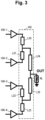
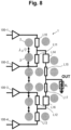
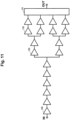
- Fig. 12 illustrates a configuration of the 4:1 multiplexer 101 in a case where the final stage of the PA has a configuration in which four unit cells 100 are parallelized.
- 2:1 multiplexing needs to be performed twice. Therefore, it is necessary to pass through two of a WC 1000 and a WC 1002 or two of a WC 1001 and the WC 1002 between the unit cells 100 and an output OUT of the PA.
- a multiplexer includes: a first impedance converter including one end and another end, the one end of the first impedance converter being connected to a first merging point of a signal input to a first input terminal and a signal input to a second input terminal, the other end of the first impedance converter being connected to an output terminal of the multiplexer; and a second impedance converter including one end and another end, the one end of the second impedance converter being connected to a second merging point of a signal input to a third input terminal and a signal input to a fourth input terminal, the other end of the second impedance converter being connected to the output terminal, in which the first impedance converter includes: a first transmission line including one end connected to the first merging point, and having a length of ⁇ /4 ( ⁇ is an in-transmission-line wavelength of a signal input to the first to the fourth input terminals) and a characteristic impedance of 35 ⁇ ; and a second transmission line including one end and another end, and having a length of
- Fig. 1 is a circuit diagram illustrating a configuration of a 4:1 multiplexer according to a first example of the present invention.
- a connection form of unit cells of a PA is the same as the configuration illustrated in Fig. 11 .
- Fig. 1 only four unit cells 100-1 to 100-4 of a final stage of the PA are illustrated.
- the output impedance of each of the unit cells 100-1 to 100-4 is 50 ⁇ .
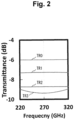
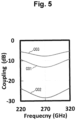
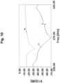
- Fig. 4 illustrates simulation results of reflection losses of the 4:1 multiplexers 1, 101, and 102 as viewed from an output terminal.
- RE1 represents a reflection loss of the 4:1 multiplexer 1
- RE2 represents a reflection loss of the 4:1 multiplexer 101
- RE3 represents a reflection loss of the 4:1 multiplexer 102. According to Fig. 4 , it can be seen that a wide band and low reflection loss can be achieved by using the 4:1 multiplexer 1 of the present example.
- TSV through silicon vias
- a planar configuration of the 4:1 multiplexer 1 is simply illustrated, but for example, a cross-sectional structure of the transmission line L15 is as illustrated in Fig. 7 .
- the 4:1 multiplexer 1 is formed on a semiconductor substrate 10, the PA being formed on the same.
- the transmission line L15 includes: a signal line 11 formed on a front surface of the semiconductor substrate 10; ground conductors 12 formed on both outer sides, respectively, of the signal line 11 on the front surface of the semiconductor substrate 10 along a propagation direction of a signal propagating through the signal line 11; and a ground conductor 13 formed on a back surface of the semiconductor substrate 10.
- the TSVs 2 penetrate the semiconductor substrate 10 and are formed to connect the ground conductors 12 and the ground conductor 13.
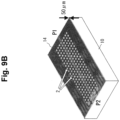
- Fig. 9A is a diagram illustrating an electric field distribution between ports P1 and P2 in a case where there is no TSV 2
- Fig. 9B is a diagram illustrating an electric field distribution between the ports P1 and P2 in a case where the TSVs 2 having an interval of 40 ⁇ m are arranged.
- Fig. 10 is a diagram illustrating simulation results of the intensity of the substrate mode signal in the case of Figs. 9A and 9B .
- the thickness of the semiconductor substrate 10 made of InP is 600 ⁇ m
- the thickness of a conductor 14 formed on the surface of the semiconductor substrate 10 is 50 ⁇ m.
Landscapes
- Engineering & Computer Science (AREA)
- Power Engineering (AREA)
- Semiconductor Integrated Circuits (AREA)
- Waveguide Connection Structure (AREA)
Applications Claiming Priority (1)
| Application Number | Priority Date | Filing Date | Title |
|---|---|---|---|
| PCT/JP2022/022768 WO2023238185A1 (ja) | 2022-06-06 | 2022-06-06 | 合波器 |
Publications (2)
| Publication Number | Publication Date |
|---|---|
| EP4539338A1 true EP4539338A1 (de) | 2025-04-16 |
| EP4539338A4 EP4539338A4 (de) | 2026-04-08 |
Family
ID=89117942
Family Applications (1)
| Application Number | Title | Priority Date | Filing Date |
|---|---|---|---|
| EP22945695.9A Pending EP4539338A4 (de) | 2022-06-06 | 2022-06-06 | Multiplexer |
Country Status (4)
| Country | Link |
|---|---|
| US (1) | US20250385415A1 (de) |
| EP (1) | EP4539338A4 (de) |
| JP (1) | JP7779386B2 (de) |
| WO (1) | WO2023238185A1 (de) |
Family Cites Families (8)
| Publication number | Priority date | Publication date | Assignee | Title |
|---|---|---|---|---|
| US5070304A (en) * | 1990-06-21 | 1991-12-03 | The United States Of America As Represented By The Secretary Of The Air Force | Distributed combiner power amplifier and method |
| US7005942B2 (en) * | 2003-11-21 | 2006-02-28 | Anaren, Inc. | Non-switching adaptable 4-way power splitter/combiner |
| JP4439474B2 (ja) * | 2006-01-17 | 2010-03-24 | セイコープレシジョン株式会社 | 無線伝搬路模擬回路 |
| JP4860638B2 (ja) * | 2008-01-18 | 2012-01-25 | 日本電業工作株式会社 | 2分配器 |
| US9912303B2 (en) * | 2010-02-03 | 2018-03-06 | Massachusetts Institute Of Technology | RF-input / RF-output outphasing amplifier |
| JP5455770B2 (ja) * | 2010-04-26 | 2014-03-26 | 三菱電機株式会社 | 電力合成分配器および電力合成分配器を用いた送信機 |
| EP3070840B1 (de) * | 2013-11-14 | 2018-10-31 | Nec Corporation | Leistungsverstärker und leistungsverstärkungsverfahren |
| US11356069B2 (en) * | 2019-10-21 | 2022-06-07 | Kabushiki Kaisha Toshiba | Digital power amplifier |
-
2022
- 2022-06-06 EP EP22945695.9A patent/EP4539338A4/de active Pending
- 2022-06-06 JP JP2024526034A patent/JP7779386B2/ja active Active
- 2022-06-06 US US18/871,253 patent/US20250385415A1/en active Pending
- 2022-06-06 WO PCT/JP2022/022768 patent/WO2023238185A1/ja not_active Ceased
Also Published As
| Publication number | Publication date |
|---|---|
| US20250385415A1 (en) | 2025-12-18 |
| EP4539338A4 (de) | 2026-04-08 |
| WO2023238185A1 (ja) | 2023-12-14 |
| JP7779386B2 (ja) | 2025-12-03 |
| JPWO2023238185A1 (de) | 2023-12-14 |
Similar Documents
| Publication | Publication Date | Title |
|---|---|---|
| US6236272B1 (en) | Traveling wave power combiner and radio base station | |
| EP2426817A1 (de) | Breitbandleistungsverstärker | |
| CN101699652B (zh) | 对称耦合波导行波功率合成放大器 | |
| US20210152130A1 (en) | Doherty power amplifier devices having intergrated output combining networks | |
| US20140125425A1 (en) | Compact microstrip to waveguide dual coupler transition | |
| CN111342817A (zh) | 阻抗控制单元、巴伦单元、电子器件和多尔蒂放大器 | |
| US5187447A (en) | Combiner/divider networks | |
| KR101155860B1 (ko) | 브랜치 라인 커플러 | |
| EP4539338A1 (de) | Multiplexer | |
| Romstadt et al. | Comparison on spectral purity of two SiGe D-Band frequency octuplers in MIMO radar MMICs | |
| CN1774832B (zh) | 用于分配滤波器输出信号的设备 | |
| CN201556693U (zh) | 一种对称耦合波导行波功率合成放大器 | |
| Bao et al. | A 63-73 GHz GaN power amplifier with a compact power combiner | |
| Tserng et al. | Microwave power GaAs FET amplifiers | |
| CN115084818A (zh) | 一种紧凑型毫米波八路波导功率合成网络 | |
| EP1209756B1 (de) | Radiofrequenz-Verstärkerschaltung | |
| Romstadt et al. | A 377–416 GHz push-push frequency doubler with driving stage and transformer-based mode separation in SiGe BiCMOS | |
| Hamani et al. | Ultra-broadband SIW diplexer on low-cost laminate technology for channel bonding D-band front ends | |
| Stones | Analysis and design of a novel microstrip-to-waveguide transition/combiner | |
| US12244051B2 (en) | Ultra-small size broadband coupler | |
| US5146175A (en) | Combining technique for a multistage, parallel amplifier | |
| US20250202434A1 (en) | Amplifier circuit | |
| KR100682478B1 (ko) | 싸이드 피드를 적용하여 고조파를 제거하는 패치 안테나와패치 안테나를 적용한 체배기 | |
| CN114285429B (zh) | 一种二次谐波抑制较高的宽带接收组件 | |
| Johannes et al. | Integrated 75-100 GHz In-Band Full-Duplex Front End GaN MMIC |
Legal Events
| Date | Code | Title | Description |
|---|---|---|---|
| STAA | Information on the status of an ep patent application or granted ep patent |
Free format text: STATUS: THE INTERNATIONAL PUBLICATION HAS BEEN MADE |
|
| PUAI | Public reference made under article 153(3) epc to a published international application that has entered the european phase |
Free format text: ORIGINAL CODE: 0009012 |
|
| STAA | Information on the status of an ep patent application or granted ep patent |
Free format text: STATUS: REQUEST FOR EXAMINATION WAS MADE |
|
| 17P | Request for examination filed |
Effective date: 20241204 |
|
| AK | Designated contracting states |
Kind code of ref document: A1 Designated state(s): AL AT BE BG CH CY CZ DE DK EE ES FI FR GB GR HR HU IE IS IT LI LT LU LV MC MK MT NL NO PL PT RO RS SE SI SK SM TR |
|
| DAV | Request for validation of the european patent (deleted) | ||
| DAX | Request for extension of the european patent (deleted) | ||
| RAP3 | Party data changed (applicant data changed or rights of an application transferred) |
Owner name: NTT, INC. |
|
| A4 | Supplementary search report drawn up and despatched |
Effective date: 20260311 |
|
| RIC1 | Information provided on ipc code assigned before grant |
Ipc: H03H 7/48 20060101AFI20260305BHEP Ipc: H03F 1/56 20060101ALN20260305BHEP Ipc: H03F 3/24 20060101ALN20260305BHEP Ipc: H03H 7/38 20060101ALN20260305BHEP |