EP4535937A2 - Komponententräger mit elektronischen komponenten und thermisch leitfähigen blöcken auf beiden seiten - Google Patents
Komponententräger mit elektronischen komponenten und thermisch leitfähigen blöcken auf beiden seiten Download PDFInfo
- Publication number
- EP4535937A2 EP4535937A2 EP25159564.1A EP25159564A EP4535937A2 EP 4535937 A2 EP4535937 A2 EP 4535937A2 EP 25159564 A EP25159564 A EP 25159564A EP 4535937 A2 EP4535937 A2 EP 4535937A2
- Authority
- EP
- European Patent Office
- Prior art keywords
- electronic component
- block
- component carrier
- component
- electrically conductive
- Prior art date
- Legal status (The legal status is an assumption and is not a legal conclusion. Google has not performed a legal analysis and makes no representation as to the accuracy of the status listed.)
- Pending
Links
Images


Classifications
-
- H—ELECTRICITY
- H10—SEMICONDUCTOR DEVICES; ELECTRIC SOLID-STATE DEVICES NOT OTHERWISE PROVIDED FOR
- H10W—GENERIC PACKAGES, INTERCONNECTIONS, CONNECTORS OR OTHER CONSTRUCTIONAL DETAILS OF DEVICES COVERED BY CLASS H10
- H10W70/00—Package substrates; Interposers; Redistribution layers [RDL]
- H10W70/60—Insulating or insulated package substrates; Interposers; Redistribution layers
- H10W70/611—Insulating or insulated package substrates; Interposers; Redistribution layers for connecting multiple chips together
- H10W70/614—Insulating or insulated package substrates; Interposers; Redistribution layers for connecting multiple chips together the multiple chips being integrally enclosed
-
- H—ELECTRICITY
- H05—ELECTRIC TECHNIQUES NOT OTHERWISE PROVIDED FOR
- H05K—PRINTED CIRCUITS; CASINGS OR CONSTRUCTIONAL DETAILS OF ELECTRIC APPARATUS; MANUFACTURE OF ASSEMBLAGES OF ELECTRICAL COMPONENTS
- H05K1/00—Printed circuits
- H05K1/18—Printed circuits structurally associated with non-printed electric components
- H05K1/182—Printed circuits structurally associated with non-printed electric components associated with components mounted in printed circuit boards [PCB], e.g. insert-mounted components [IMC]
- H05K1/185—Printed circuits structurally associated with non-printed electric components associated with components mounted in printed circuit boards [PCB], e.g. insert-mounted components [IMC] associated with components encapsulated in the insulating substrate of the PCBs; associated with components incorporated in internal layers of multilayer circuit boards
-
- H—ELECTRICITY
- H05—ELECTRIC TECHNIQUES NOT OTHERWISE PROVIDED FOR
- H05K—PRINTED CIRCUITS; CASINGS OR CONSTRUCTIONAL DETAILS OF ELECTRIC APPARATUS; MANUFACTURE OF ASSEMBLAGES OF ELECTRICAL COMPONENTS
- H05K1/00—Printed circuits
- H05K1/02—Details
- H05K1/0201—Thermal arrangements, e.g. for cooling, heating or preventing overheating
- H05K1/0203—Cooling of mounted components
- H05K1/0204—Cooling of mounted components using means for thermal conduction connection in the thickness direction of the substrate
- H05K1/0206—Cooling of mounted components using means for thermal conduction connection in the thickness direction of the substrate by printed thermal vias
-
- H—ELECTRICITY
- H10—SEMICONDUCTOR DEVICES; ELECTRIC SOLID-STATE DEVICES NOT OTHERWISE PROVIDED FOR
- H10W—GENERIC PACKAGES, INTERCONNECTIONS, CONNECTORS OR OTHER CONSTRUCTIONAL DETAILS OF DEVICES COVERED BY CLASS H10
- H10W40/00—Arrangements for thermal protection or thermal control
- H10W40/20—Arrangements for cooling
- H10W40/25—Arrangements for cooling characterised by their materials
- H10W40/255—Arrangements for cooling characterised by their materials having a laminate or multilayered structure, e.g. direct bond copper [DBC] ceramic substrates
-
- H—ELECTRICITY
- H10—SEMICONDUCTOR DEVICES; ELECTRIC SOLID-STATE DEVICES NOT OTHERWISE PROVIDED FOR
- H10W—GENERIC PACKAGES, INTERCONNECTIONS, CONNECTORS OR OTHER CONSTRUCTIONAL DETAILS OF DEVICES COVERED BY CLASS H10
- H10W70/00—Package substrates; Interposers; Redistribution layers [RDL]
- H10W70/60—Insulating or insulated package substrates; Interposers; Redistribution layers
- H10W70/611—Insulating or insulated package substrates; Interposers; Redistribution layers for connecting multiple chips together
-
- H—ELECTRICITY
- H10—SEMICONDUCTOR DEVICES; ELECTRIC SOLID-STATE DEVICES NOT OTHERWISE PROVIDED FOR
- H10W—GENERIC PACKAGES, INTERCONNECTIONS, CONNECTORS OR OTHER CONSTRUCTIONAL DETAILS OF DEVICES COVERED BY CLASS H10
- H10W70/00—Package substrates; Interposers; Redistribution layers [RDL]
- H10W70/60—Insulating or insulated package substrates; Interposers; Redistribution layers
- H10W70/62—Insulating or insulated package substrates; Interposers; Redistribution layers characterised by their interconnections
- H10W70/63—Vias, e.g. via plugs
- H10W70/635—Through-vias
-
- H—ELECTRICITY
- H10—SEMICONDUCTOR DEVICES; ELECTRIC SOLID-STATE DEVICES NOT OTHERWISE PROVIDED FOR
- H10W—GENERIC PACKAGES, INTERCONNECTIONS, CONNECTORS OR OTHER CONSTRUCTIONAL DETAILS OF DEVICES COVERED BY CLASS H10
- H10W90/00—Package configurations
-
- H—ELECTRICITY
- H05—ELECTRIC TECHNIQUES NOT OTHERWISE PROVIDED FOR
- H05K—PRINTED CIRCUITS; CASINGS OR CONSTRUCTIONAL DETAILS OF ELECTRIC APPARATUS; MANUFACTURE OF ASSEMBLAGES OF ELECTRICAL COMPONENTS
- H05K2201/00—Indexing scheme relating to printed circuits covered by H05K1/00
- H05K2201/10—Details of components or other objects attached to or integrated in a printed circuit board
- H05K2201/10007—Types of components
- H05K2201/10166—Transistor
-
- H—ELECTRICITY
- H05—ELECTRIC TECHNIQUES NOT OTHERWISE PROVIDED FOR
- H05K—PRINTED CIRCUITS; CASINGS OR CONSTRUCTIONAL DETAILS OF ELECTRIC APPARATUS; MANUFACTURE OF ASSEMBLAGES OF ELECTRICAL COMPONENTS
- H05K2201/00—Indexing scheme relating to printed circuits covered by H05K1/00
- H05K2201/10—Details of components or other objects attached to or integrated in a printed circuit board
- H05K2201/10227—Other objects, e.g. metallic pieces
- H05K2201/10416—Metallic blocks or heatsinks completely inserted in a PCB
-
- H—ELECTRICITY
- H05—ELECTRIC TECHNIQUES NOT OTHERWISE PROVIDED FOR
- H05K—PRINTED CIRCUITS; CASINGS OR CONSTRUCTIONAL DETAILS OF ELECTRIC APPARATUS; MANUFACTURE OF ASSEMBLAGES OF ELECTRICAL COMPONENTS
- H05K2203/00—Indexing scheme relating to apparatus or processes for manufacturing printed circuits covered by H05K3/00
- H05K2203/06—Lamination
- H05K2203/061—Lamination of previously made multilayered subassemblies
-
- H—ELECTRICITY
- H05—ELECTRIC TECHNIQUES NOT OTHERWISE PROVIDED FOR
- H05K—PRINTED CIRCUITS; CASINGS OR CONSTRUCTIONAL DETAILS OF ELECTRIC APPARATUS; MANUFACTURE OF ASSEMBLAGES OF ELECTRICAL COMPONENTS
- H05K2203/00—Indexing scheme relating to apparatus or processes for manufacturing printed circuits covered by H05K3/00
- H05K2203/14—Related to the order of processing steps
- H05K2203/1461—Applying or finishing the circuit pattern after another process, e.g. after filling of vias with conductive paste, after making printed resistors
- H05K2203/1469—Circuit made after mounting or encapsulation of the components
-
- H—ELECTRICITY
- H05—ELECTRIC TECHNIQUES NOT OTHERWISE PROVIDED FOR
- H05K—PRINTED CIRCUITS; CASINGS OR CONSTRUCTIONAL DETAILS OF ELECTRIC APPARATUS; MANUFACTURE OF ASSEMBLAGES OF ELECTRICAL COMPONENTS
- H05K3/00—Apparatus or processes for manufacturing printed circuits
- H05K3/40—Forming printed elements for providing electric connections to or between printed circuits
- H05K3/42—Plated through-holes or plated via connections
- H05K3/429—Plated through-holes specially for multilayer circuits, e.g. having connections to inner circuit layers
-
- H—ELECTRICITY
- H05—ELECTRIC TECHNIQUES NOT OTHERWISE PROVIDED FOR
- H05K—PRINTED CIRCUITS; CASINGS OR CONSTRUCTIONAL DETAILS OF ELECTRIC APPARATUS; MANUFACTURE OF ASSEMBLAGES OF ELECTRICAL COMPONENTS
- H05K3/00—Apparatus or processes for manufacturing printed circuits
- H05K3/46—Manufacturing multilayer circuits
- H05K3/4644—Manufacturing multilayer circuits by building the multilayer layer by layer, i.e. build-up multilayer circuits
- H05K3/4652—Adding a circuit layer by laminating a metal foil or a preformed metal foil pattern
-
- H—ELECTRICITY
- H10—SEMICONDUCTOR DEVICES; ELECTRIC SOLID-STATE DEVICES NOT OTHERWISE PROVIDED FOR
- H10W—GENERIC PACKAGES, INTERCONNECTIONS, CONNECTORS OR OTHER CONSTRUCTIONAL DETAILS OF DEVICES COVERED BY CLASS H10
- H10W70/00—Package substrates; Interposers; Redistribution layers [RDL]
- H10W70/01—Manufacture or treatment
- H10W70/05—Manufacture or treatment of insulating or insulated package substrates, or of interposers, or of redistribution layers
- H10W70/093—Connecting or disconnecting other interconnections thereto or therefrom, e.g. connecting bond wires or bumps
-
- H—ELECTRICITY
- H10—SEMICONDUCTOR DEVICES; ELECTRIC SOLID-STATE DEVICES NOT OTHERWISE PROVIDED FOR
- H10W—GENERIC PACKAGES, INTERCONNECTIONS, CONNECTORS OR OTHER CONSTRUCTIONAL DETAILS OF DEVICES COVERED BY CLASS H10
- H10W70/00—Package substrates; Interposers; Redistribution layers [RDL]
- H10W70/099—Connecting interconnections to insulating or insulated package substrates, interposers or redistribution layers
-
- H—ELECTRICITY
- H10—SEMICONDUCTOR DEVICES; ELECTRIC SOLID-STATE DEVICES NOT OTHERWISE PROVIDED FOR
- H10W—GENERIC PACKAGES, INTERCONNECTIONS, CONNECTORS OR OTHER CONSTRUCTIONAL DETAILS OF DEVICES COVERED BY CLASS H10
- H10W72/00—Interconnections or connectors in packages
- H10W72/071—Connecting or disconnecting
- H10W72/073—Connecting or disconnecting of die-attach connectors
- H10W72/07331—Connecting techniques
-
- H—ELECTRICITY
- H10—SEMICONDUCTOR DEVICES; ELECTRIC SOLID-STATE DEVICES NOT OTHERWISE PROVIDED FOR
- H10W—GENERIC PACKAGES, INTERCONNECTIONS, CONNECTORS OR OTHER CONSTRUCTIONAL DETAILS OF DEVICES COVERED BY CLASS H10
- H10W72/00—Interconnections or connectors in packages
- H10W72/30—Die-attach connectors
- H10W72/351—Materials of die-attach connectors
- H10W72/352—Materials of die-attach connectors comprising metals or metalloids, e.g. solders
-
- H—ELECTRICITY
- H10—SEMICONDUCTOR DEVICES; ELECTRIC SOLID-STATE DEVICES NOT OTHERWISE PROVIDED FOR
- H10W—GENERIC PACKAGES, INTERCONNECTIONS, CONNECTORS OR OTHER CONSTRUCTIONAL DETAILS OF DEVICES COVERED BY CLASS H10
- H10W72/00—Interconnections or connectors in packages
- H10W72/851—Dispositions of multiple connectors or interconnections
- H10W72/874—On different surfaces
-
- H—ELECTRICITY
- H10—SEMICONDUCTOR DEVICES; ELECTRIC SOLID-STATE DEVICES NOT OTHERWISE PROVIDED FOR
- H10W—GENERIC PACKAGES, INTERCONNECTIONS, CONNECTORS OR OTHER CONSTRUCTIONAL DETAILS OF DEVICES COVERED BY CLASS H10
- H10W72/00—Interconnections or connectors in packages
- H10W72/90—Bond pads, in general
- H10W72/941—Dispositions of bond pads
- H10W72/9413—Dispositions of bond pads on encapsulations
-
- H—ELECTRICITY
- H10—SEMICONDUCTOR DEVICES; ELECTRIC SOLID-STATE DEVICES NOT OTHERWISE PROVIDED FOR
- H10W—GENERIC PACKAGES, INTERCONNECTIONS, CONNECTORS OR OTHER CONSTRUCTIONAL DETAILS OF DEVICES COVERED BY CLASS H10
- H10W90/00—Package configurations
- H10W90/10—Configurations of laterally-adjacent chips
-
- H—ELECTRICITY
- H10—SEMICONDUCTOR DEVICES; ELECTRIC SOLID-STATE DEVICES NOT OTHERWISE PROVIDED FOR
- H10W—GENERIC PACKAGES, INTERCONNECTIONS, CONNECTORS OR OTHER CONSTRUCTIONAL DETAILS OF DEVICES COVERED BY CLASS H10
- H10W90/00—Package configurations
- H10W90/701—Package configurations characterised by the relative positions of pads or connectors relative to package parts
- H10W90/731—Package configurations characterised by the relative positions of pads or connectors relative to package parts of die-attach connectors
- H10W90/734—Package configurations characterised by the relative positions of pads or connectors relative to package parts of die-attach connectors between a chip and a stacked insulating package substrate, interposer or RDL
Definitions
- the invention relates to methods of manufacturing a component carrier, and to component carriers.
- component carriers equipped with one or more electronic components and increasing miniaturization of such components as well as a rising number of components to be mounted on or embedded in the component carriers such as printed circuit boards
- increasingly more powerful array-like components or packages having several components are being employed, which have a plurality of contacts or connections, with ever smaller spacing between these contacts. Removal of heat generated by such components and the component carrier itself during operation becomes an increasing issue.
- component carriers shall be mechanically robust and electrically reliable so as to be operable even under harsh conditions.
- a component carrier comprising at least one electrically conductive layer structure and/or at least one electrically insulating layer structure, a first electronic component and a second electronic component arranged (and in particular laminated) in the stack, a first block and a second block arranged (and in particular laminated) in the stack below the first electronic component and the second electronic component, and a third block and a fourth block arranged (and in particular laminated) in the stack above the first electronic component and the second electronic component, wherein said blocks are thermally conductive (and in particular at least partially electrically conductive).
- layer structure may particularly denote a continuous layer, a patterned layer or a plurality of nonconsecutive islands within a common plane.
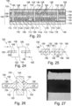
- nail head structure may particularly denote a portion of the block being shaped, in a cross-sectional view of the component carrier, as a horizontally aligned nail head (see for instance Figure 26 ). More specifically, such a nail head structure may have, in the cross-sectional view of the component carrier, a tapering portion tapering inwardly from the vertical hole towards a narrower rectangular portion. At the end of the nail head structure with its largest diameter in the cross-sectional view, the nail head structure may have a vertical line. Descriptively speaking, such a nail head structure may be formed by creating the vertical hole extending through the entire block with sufficient energy impact during the hole formation process.
- electrically conductive contact structure may particularly denote a member or a material being electrically conductive, being arranged in only part of (for instance only covering sidewalls of) or in the entire vertical hole and being in direct physical contact with the block through which the vertical hole extends so that electric current can be conducted between the electrically conductive contact structure and the block.
- a component carrier which has embedded in an interior thereof, in particular completely within stack material, electronic components such as silicon chips, and highly conductive blocks connected to the electronic components.
- the embedded electronic components and the embedded blocks may be thermally and/or electrically coupled with one another.
- the blocks may be embedded, for instance by lamination, into the stack. However, it is also possible to in-situ manufacture the copper blocks during the processing. Instead of embedding copper blocks, a thick copper foil can be applied (also by lamination), and recesses between the blocks can be etched away.
- first electronic component and the second electronic component may be located at the same vertical level, and in particular on and/or in the same layer structure(s) of the stack. It may also be possible that the first block and the second block are located at the same vertical level, and in particular on and/or in the same layer structure(s) of the stack. Additionally or alternatively, it may be possible that the third block and the fourth block are located at the same vertical level, and in particular on and/or in the same layer structure(s) of the stack.
- the first electronic component may be thermally and/or electrically coupled with the first block and the third block.
- the second electronic component may be thermally and/or electrically coupled with the second block and the fourth block. The first electronic component and the second electronic component may be electrically coupled.
- the stack comprises only laminated layer structures.
- the stack may be free of mold compound.
- a core may denote a thick and fully cured electrically insulating layer structure.
- the use of three cores for accommodating the components and the blocks may allow to implement separate technologies for handling the thermally conductive and at least partially electrically conductive blocks (such as copper blocks handled in PCB technology) on the one hand, and the assembly of the electronic components (for instance sinter connecting MOSFETs) on the other hand.
- the copper blocks are manufactured in-situ or as self-made copper blocks.
- the first electronic component and the second electronic component operate with a vertical current flow between opposing main surfaces thereof.
- each of the electronic components may be embodied as semiconductor chip with vertical current flow.
- an electronic component embodied as field-effect transistor chip may have a source pad and a gate pad on one main surface and a drain pad on the opposing other main surface. During operation, the electric current may then flow through the semiconductor body between the pads on the two opposing main surfaces.
- the implementation of electronic components with vertical current flow may keep the component carrier compact and may reduce the parasitic capacitance.
- the component carrier comprises a continuous electrically conductive path which includes the at least one electrically conductive layer structure, said blocks, the first electronic component and the second electronic component.
- said blocks may advantageously contribute to an electric function of the component carrier in addition to their thermal heat removal capability.
- the contact structure may comprise a plated metal structure.
- the contact structure is embodied as a separate member such as a metal pin which may be inserted or pressed into the vertical hole. After formation of the vertical hole, a pre-formed metallic pin may thus be inserted into the vertical hole to thereby form or establish an electrically and thermally conductive connection with the block traversed or penetrated by the vertical hole.
- the above mentioned continuous electrically conductive path may also include the electrically conductive structure in said vertical hole.
- a nail head structure which may be formed at an interface between the metal-filled vertical hole and the metallic block traversed entirely by the vertical hole may ensure a low ohmic connection with high contact area.
- the component carrier comprises at least one vertical hole extending through at least part of the stack and connecting, in particular electrically connecting, at least two of said blocks, in particular embodied as copper blocks, with each other. This may allow to establish short electric paths (for keeping losses small) and/or thermal paths (for efficiently removing heat).
- the first electronic component and the second electronic component are configured and are interconnected by the blocks and the at least one electrically conductive layer structure to provide a half-bridge function.
- a half-bridge may be a current converter using switches to control an output voltage.
- a half-bridge may be implemented in a motor control.
- the stack comprises a plurality of electrically insulating layer structures, wherein at least one electrically insulating layer structure (in particular an uppermost and/or a lowermost electrically insulating layer structure) of the stack has a higher thermal conductivity compared to at least one remaining electrically insulating layer structure of the stack.
- the one or more electrically insulating layer structure(s) having a higher thermal conductivity than the other(s) may be for example a thermal prepreg which may have, for example, a thermal conductivity of at least 1.0 W/mK, in particular of at least 1.8 W/mK, and preferably of at least 2 W/mK.
- the block may comprise or consists of a metal, in particular copper. Copper has turned out as particularly appropriate for creating a nail head structure with pronounced extension at the upper and at the lower side when impacted preferably by a mechanical drill bit (or alternatively by a laser beam) introducing thermal energy in the block during drilling.
- the block used for the formation of a nail head structure comprises a metal coated ceramic.
- the component carrier is shaped as a plate. This contributes to the compact design, wherein the component carrier nevertheless provides a large basis for mounting components thereon. Furthermore, in particular a naked die as example for an embedded electronic component, can be conveniently embedded, thanks to its small thickness, into a thin plate such as a printed circuit board.
- the component carrier is configured as one of the group consisting of a printed circuit board, a substrate (in particular an IC substrate), and an interposer.
- prepreg A semi-cured resin in combination with a reinforcing agent, e.g. fibers impregnated with the above-mentioned resins is called prepreg.
- FR4 FR4
- FR5 which describe their flame retardant properties.
- prepreg particularly FR4 are usually preferred for rigid PCBs, other materials, in particular epoxy-based build-up materials (such as build-up films) or photoimageable dielectric materials, may be used as well.
- high-frequency materials such as polytetrafluoroethylene, liquid crystal polymer and/or cyanate ester resins, may be preferred.
- LTCC low temperature cofired ceramics
- other low, very low or ultra-low DK materials may be applied in the component carrier as electrically insulating structures.
- a component can be an active electronic component (having at least one p-n-junction implemented), a passive electronic component such as a resistor, an inductance, or capacitor, an electronic chip, a storage device (for instance a DRAM or another data memory), a filter, an integrated circuit (such as field-programmable gate array (FPGA), programmable array logic (PAL), generic array logic (GAL) and complex programmable logic devices (CPLDs)), a signal processing component, a power management component (such as a field-effect transistor (FET), metal-oxide-semiconductor field-effect transistor (MOSFET), complementary metal-oxide-semiconductor (CMOS), junction field-effect transistor (JFET), or insulated-gate field-effect transistor (IGFET), all based on semiconductor materials such as silicon carbide (SiC), gallium arsenide (GaAs), gallium nitride (GaN), gallium oxide (Ga 2 O 3 ), indium gallium ars
- a magnetic element can be used as a component.
- a magnetic element may be a permanent magnetic element (such as a ferromagnetic element, an antiferromagnetic element, a multiferroic element or a ferrimagnetic element, for instance a ferrite core) or may be a paramagnetic element.
- the component may also be a IC substrate, an interposer or a further component carrier, for example in a board-in-board configuration.
- the component may be surface mounted on the component carrier and/or may be embedded in an interior thereof.
- other components in particular those which generate and emit electromagnetic radiation and/or are sensitive with regard to electromagnetic radiation propagating from an environment, may be used as component.
- the component carrier is a laminate-type component carrier.
- the component carrier is a compound of multiple layer structures which are stacked and connected together by applying a pressing force and/or heat.
- an electrically insulating solder resist may be applied to one or both opposing main surfaces of the layer stack or component carrier in terms of surface treatment. For instance, it is possible to form such a solder resist on an entire main surface and to subsequently pattern the layer of solder resist so as to expose one or more electrically conductive surface portions which shall be used for electrically coupling the component carrier to an electronic periphery. The surface portions of the component carrier remaining covered with solder resist may be efficiently protected against oxidation or corrosion, in particular surface portions containing copper.
- Such an embodiment may overcome conventional limitations in terms of current carrying capability in a horizontal plane of a component carrier caused by limited copper layer thickness (of conventionally 70 ⁇ m at the maximum). Conventionally, higher current values require multiple power layers which increases the space consumption. In contrast to such conventional approaches, exemplary embodiments of the invention may enable to transport higher current in particular along one or more vertically extending holes connected to blocks (such as metal inlays) which may extend predominantly in a horizontal plane.
- Laminating the electronic components in the stack may allow to embed or encapsulate electronic components (in particular embodied as MOSFET chips) with printed circuit board (PCB) material. This may avoid the addition of other materials such as a mold compound. In particular, it may be advantageous to use vertical through holes and metal inlays to transmit current through the module-type component carrier. Thus, the blocks may have a double function of removing heat (by increasing thermal conductivity) and conducting current.
- PCB printed circuit board
- exemplary embodiments of the invention may transport a high current in a PCB-type component carrier with embedded power components (or with an embedded system of electronic components inside) and by removing generated heat out of it in parallel.
- a component carrier with embedded thermally and electrically conductive block in which a vertical hole is formed.
- the latter may be filled at least partially with an electrically conductive contact structure, such as a copper pin or a plating structure.
- the block may be provided with a nail head structure in a contact region to the contact structure, which increases their mutual contact area and thereby reduces the thermal and electrical contact resistance.
- the nail head structure of the block may extend up to the vertical hole, i.e. may partially delimit the vertical hole along its entire perimeter.
- such a nail head structure may be formed by an energy impact during formation of the through hole extending through the entire block, in particular by mechanically drilling using a rapidly rotating drill bit or laser drilling by a pulsed or continuous highly energetic laser beam.
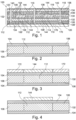
- Figure 1 illustrates a cross-sectional view of a component carrier 100 according to an exemplary embodiment of the invention.
- component carrier 100 comprises a laminated layer stack 102 composed of a plurality of electrically conductive layer structures 104 and a plurality of electrically insulating layer structures 106.
- Lamination may particularly denote the connection of the layer structures 104, 106 by the application of pressure and/or heat.
- the electrically conductive layer structure(s) 104 may comprise patterned or continuous copper foils (as shown) and vertical through-connections, for example copper filled laser vias which may be created by plating.
- the electrically insulating layer structure(s) 106 may comprise a respective resin (such as a respective epoxy resin), preferably comprising reinforcing particles therein (for instance glass fibers or glass spheres).
- the electrically insulating layer structures 106 may be made of prepreg or FR4.
- the entire stack 102 is made of laminated layer structures 104, 106 only and is free of mold compound.
- the material of the laminated layer stack 102 is substantially homogeneous and does not involve a pronounced CTE mismatch. This keeps thermal tensions and stress in an interior of the stack 102 small.
- ceramic inlays which may be cladded by metal
- DCB Direct Copper Bonding substrates or pieces may also be used as blocks 112, 114, 116, 118.
- a continuous electrically conductive path may be formed by the electrically conductive layer structures 104, the blocks 112, 114, 116, 118, the first electronic component 108 and the second electronic component 110 as well as by electrically conductive structures 140 in vertical holes 120 described below.
- blocks 112, 114, 116, 118 may fulfil a double function.
- they may contribute to the conductance of electricity through the electronic components 108, 110 in an interior of the component carrier 100.
- they may remove heat created by the electronic components 108, 110 during operation of the component carrier 100 both towards an upper main surface and a lower main surface according to Figure 1 . This may ensure an efficient double-sided cooling rendering component carrier 100 particularly appropriate for high-power applications.
- component carrier 100 has several vertical holes 120 extending from an upper main surface of the component carrier 100 through an upper part of the stack 102 and through one or two of the blocks 112, 114, 116, 118. More specifically, one of the vertical holes 120 extends only through first block 112 as well as through portions of the stack 102 above and below the first block 112. Another one of the vertical holes 120 extends only through fourth block 118 as well as through portions of the stack 102 above and below the fourth block 118. Yet another vertical hole 120 extends entirely through second block 114 and entirely through third block 116 as well as through portions of the stack 102 below second block 114, above third block 116 and between second block 114 and third block 116.
- a gate pad of a respective one of the electronic components 108, 110 may be connected with thin copper lines, whereas source pad and drain pad may be connected with thick metal (for instance by a respective block 112, 114 and the electrically conductive layer structures 104) to transfer high current and heat.
- the electronic components 108, 110 are connected on a bottom side with the blocks 112, 114, respectively, by the described connection medium 144. On a top side, the electronic components 108, 110 may be connected by microvias.
- a lowermost electrically insulating layer structure 106' of the stack 102 may be a thermal prepreg which has a higher thermal conductivity (for example 1.8 W/mK) compared to the other electrically insulating layer structures 106 of the stack 102 which may have a lower thermal conductivity (for example 0.8 W/mK).
- Said thermal prepreg layer may provide a pronounced contribution to the heat removal towards a cooling unit 170.
- stack 102 may be mounted on the cooling unit 170 (such as a heat sink) with a thermal interface material 176 (which may be thermally conductive and electrically insulating) in between.
- the cooling unit 170 such as a heat sink
- a thermal interface material 176 which may be thermally conductive and electrically insulating
- core 132 is shown as a thick and fully cured electrically insulating layer structure 106 (in particular made of FR4) having electrically conductive layer structures 104 attached to both opposing main surfaces thereof, for example copper foils.
- First block 112 is embedded in the core 132.
- core 132 may be fabricated with an embedded copper (or aluminum nitride) cuboid as first block 112.
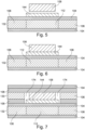
- Figure 3 shows a sinter depot printed as connection medium 144 on top of the structure shown in Figure 2 using a stencil printing mask 172.
- connection medium 144 embodied as sinter depot.
- Figure 5 shows how the first electronic component 108 is mounted or assembled on the connection medium 144. This may be accomplished by a pick and place process.
- the first electronic component 108 for instance a MOSFET formed in silicon, GaN or SiC technology, an IGBT, or a diode
- the sinter depot compare Figure 6 . It may be optionally possible to apply mechanical pressure and/or raise the temperature during assembly of the first electronic component 108 to promote adhesion on the connection medium 144.
- a fully cured core 130 (for instance fully cured FR4) covered on both opposing main surfaces thereof with a respective at least partially uncured electrically insulating layer structure 106 (such as B-stage prepreg or resin) and having an additional electrically conductive layer structure 104 (such as a copper foil) on top may be provided with a recess or cavity 174 and may be placed on top of the structure of Figure 6 . More specifically, cavity 174 may be formed in core 130 and in the lower uncured electrically insulating layer structure 106 to thereby form a cap structure. As a result of putting the cap structure on the structure shown in Figure 6 , the first electronic component 108 and the connection medium 144 are accommodated in the cavity 174. Thus, a lay-up of a pre-cut prepreg, a pre-cut core 130 (optionally with structured copper layer, not shown), a continuous sheet of prepreg and a continuous copper foil may be provided and placed on top of the electronic component 108.
- a further electrically conductive layer structure 104 such as the copper foil
- a further uncured electrically insulating layer structure 106 such as a prepreg sheet
- a lay-up of prepreg in this embodiment a normal prepreg
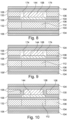
- the standard prepreg used as lowermost electrically insulating layer structure 106 may have a thermal conductivity of not more than 1.0 W/mK, in particular of not more than 0.8 W/mK. Thermal vias may be formed on a bottom side.
- Figure 9 is an alternative to the structure according to Figure 8 and may also be obtained based on the structure shown in Figure 7 .
- a thermal prepreg may be applied as uncured electrically insulating layer structure 106' at a bottom side, together with a further electrically conductive layer structure 104.
- the thermal prepreg may have a thermal conductivity of more than 1.0 W/mK, in particular of more than 1.8 W/mK.
- no thermal vias are formed on the bottom side of the structure of Figure 9 .
- Figure 8 and Figure 9 differ concerning the thermal conductivity of the lowermost electrically insulating layer structures 106/106' and/or concerning the presence or absence of thermal vias.
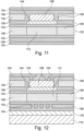
- a lamination process may be carried out by the application of pressure and/or heat. Cavities 174 are filled with resin from the previously uncured electrically insulating layer structures 106 during the lamination process.
- the two at least partially uncured electrically insulating layer structures 106 may become flowable during lamination and may thus flow into cavity 174.
- said previously uncured electrically insulating layer structures 106 may be cured (for instance by polymerizing, cross-linking, etc.) and may thereby be re-solidified.
- Figure 10 shows the result of the lamination process starting from the embodiment according to Figure 8 .
- Figure 11 shows the result of the lamination process starting from the alternative embodiment according to Figure 9 .
- the obtained drill holes may be filled with electrically conductive material such as copper, for instance by plating.
- the exterior electrically conductive layer structures 104 may then be structured to thereby obtain a patterned metal layer.
- the stack 102 may be mounted on a cooling unit 170, preferably with a thermal interface material 176 between the stack 102 and the cooling unit 170.
- the manufacturing process may proceed with applying a connection medium 144 (such as a sinter depot) on the stack-up, i.e. on the upper main surface of the processed layer stack.
- a connection medium 144 such as a sinter depot
- a further thermally conductive and electrically conductive block 116 may be embedded in a further core 134 which may be cladded with patterned further electrically conductive layer structures 104 on both sides.
- Figure 24 illustrates a cross-sectional view
- Figure 25 illustrates a plan view showing a path 136 of electric current flowing through a component carrier 100 according to an exemplary embodiment of the invention, in particular the one shown in Figure 1 or in Figure 23 .
- Figure 26 illustrates a cross-sectional view of a part of a component carrier 100 according to still another exemplary embodiment of the invention.
- the features described in the following referring to Figure 26 may be implemented as well in other embodiments of the invention, for instance the ones of Figure 1 or Figure 23 . More specifically, Figure 26 shows a detail of component carrier 100 around an intersection between a metal-filled vertical through hole 120 and a copper block 112 traversed by said metal-filled vertical through hole 120.
Landscapes
- Engineering & Computer Science (AREA)
- Microelectronics & Electronic Packaging (AREA)
- Cooling Or The Like Of Semiconductors Or Solid State Devices (AREA)
- Manufacturing & Machinery (AREA)
- Chemical & Material Sciences (AREA)
- Ceramic Engineering (AREA)
- Structures For Mounting Electric Components On Printed Circuit Boards (AREA)
Priority Applications (1)
| Application Number | Priority Date | Filing Date | Title |
|---|---|---|---|
| EP25159564.1A EP4535937A3 (de) | 2020-11-05 | 2020-11-05 | Komponententräger mit elektronischen komponenten und thermisch leitfähigen blöcken auf beiden seiten |
Applications Claiming Priority (2)
| Application Number | Priority Date | Filing Date | Title |
|---|---|---|---|
| EP20205934.1A EP3996473B1 (de) | 2020-11-05 | 2020-11-05 | Komponententräger mit elektronischen komponenten und thermisch leitfähigen blöcken auf beiden seiten |
| EP25159564.1A EP4535937A3 (de) | 2020-11-05 | 2020-11-05 | Komponententräger mit elektronischen komponenten und thermisch leitfähigen blöcken auf beiden seiten |
Related Parent Applications (2)
| Application Number | Title | Priority Date | Filing Date |
|---|---|---|---|
| EP20205934.1A Division EP3996473B1 (de) | 2020-11-05 | 2020-11-05 | Komponententräger mit elektronischen komponenten und thermisch leitfähigen blöcken auf beiden seiten |
| EP20205934.1A Division-Into EP3996473B1 (de) | 2020-11-05 | 2020-11-05 | Komponententräger mit elektronischen komponenten und thermisch leitfähigen blöcken auf beiden seiten |
Publications (2)
| Publication Number | Publication Date |
|---|---|
| EP4535937A2 true EP4535937A2 (de) | 2025-04-09 |
| EP4535937A3 EP4535937A3 (de) | 2025-06-25 |
Family
ID=73138702
Family Applications (3)
| Application Number | Title | Priority Date | Filing Date |
|---|---|---|---|
| EP25159564.1A Pending EP4535937A3 (de) | 2020-11-05 | 2020-11-05 | Komponententräger mit elektronischen komponenten und thermisch leitfähigen blöcken auf beiden seiten |
| EP20205934.1A Active EP3996473B1 (de) | 2020-11-05 | 2020-11-05 | Komponententräger mit elektronischen komponenten und thermisch leitfähigen blöcken auf beiden seiten |
| EP21807037.3A Pending EP4241540A1 (de) | 2020-11-05 | 2021-11-05 | Komponententräger mit elektronischen komponenten und thermisch leitfähigen blöcken auf beiden seiten |
Family Applications After (2)
| Application Number | Title | Priority Date | Filing Date |
|---|---|---|---|
| EP20205934.1A Active EP3996473B1 (de) | 2020-11-05 | 2020-11-05 | Komponententräger mit elektronischen komponenten und thermisch leitfähigen blöcken auf beiden seiten |
| EP21807037.3A Pending EP4241540A1 (de) | 2020-11-05 | 2021-11-05 | Komponententräger mit elektronischen komponenten und thermisch leitfähigen blöcken auf beiden seiten |
Country Status (4)
| Country | Link |
|---|---|
| US (1) | US20240014142A1 (de) |
| EP (3) | EP4535937A3 (de) |
| CN (1) | CN116711469A (de) |
| WO (1) | WO2022096638A1 (de) |
Families Citing this family (9)
| Publication number | Priority date | Publication date | Assignee | Title |
|---|---|---|---|---|
| JP2023079124A (ja) * | 2021-11-26 | 2023-06-07 | 国立大学法人東北大学 | パワー半導体素子及びパワー半導体モジュール |
| CN114725021B (zh) * | 2022-05-12 | 2026-04-07 | 深圳大学 | 一种基于GaOx-NMOS/GaN-PMOS的CMOS反相器的制备方法 |
| CN114725020B (zh) * | 2022-05-12 | 2026-04-07 | 深圳大学 | 一种基于GaOx-PMOS/GaN-NMOS的CMOS反相器的制备方法 |
| US20240112978A1 (en) * | 2022-09-29 | 2024-04-04 | Advanced Semiconductor Engineering, Inc. | Electronic package |
| US12284792B2 (en) * | 2023-02-23 | 2025-04-22 | Toyota Motor Engineering & Manufacturing North America, Inc. | Power electronics assemblies having power electronics devices embedded within a flip chip |
| WO2025011781A1 (en) * | 2023-07-07 | 2025-01-16 | Microchip Technology Caldicot Limited | Substrate with embedded conductive coin |
| TWI890140B (zh) * | 2023-09-18 | 2025-07-11 | 聚燁科技股份有限公司 | 導熱基板 |
| EP4530606A1 (de) * | 2023-09-26 | 2025-04-02 | Infineon Technologies AG | Halbleiterbauelemente, gassensor mit mikroelektromechanischem system, verfahren |
| CN121035084B (zh) * | 2025-10-31 | 2026-02-10 | 广东芯聚能半导体有限公司 | 嵌入式功率模块 |
Family Cites Families (14)
| Publication number | Priority date | Publication date | Assignee | Title |
|---|---|---|---|---|
| US5654587A (en) * | 1993-07-15 | 1997-08-05 | Lsi Logic Corporation | Stackable heatsink structure for semiconductor devices |
| US5773886A (en) * | 1993-07-15 | 1998-06-30 | Lsi Logic Corporation | System having stackable heat sink structures |
| US5693981A (en) * | 1993-12-14 | 1997-12-02 | Lsi Logic Corporation | Electronic system with heat dissipating apparatus and method of dissipating heat in an electronic system |
| US5514327A (en) * | 1993-12-14 | 1996-05-07 | Lsi Logic Corporation | Powder metal heat sink for integrated circuit devices |
| US5641944A (en) * | 1995-09-29 | 1997-06-24 | Allen-Bradley Company, Inc. | Power substrate with improved thermal characteristics |
| US6622786B1 (en) * | 2002-04-17 | 2003-09-23 | International Business Machines Corporation | Heat sink structure with pyramidic and base-plate cut-outs |
| KR100796523B1 (ko) * | 2006-08-17 | 2008-01-21 | 삼성전기주식회사 | 전자부품 내장형 다층 인쇄배선기판 및 그 제조방법 |
| US20110044004A1 (en) * | 2009-08-18 | 2011-02-24 | Garosshen Thomas J | Heat transfer apparatus having a thermal interface material |
| US20150214127A1 (en) * | 2014-01-24 | 2015-07-30 | Qualcomm Incorporated | Integrated device comprising a substrate with aligning trench and/or cooling cavity |
| US9681558B2 (en) * | 2014-08-12 | 2017-06-13 | Infineon Technologies Ag | Module with integrated power electronic circuitry and logic circuitry |
| EP2988328B1 (de) * | 2014-08-19 | 2021-05-12 | ABB Schweiz AG | Leistungshalbleitermodul und Verfahren zur Herstellung davon |
| JP2016149475A (ja) * | 2015-02-13 | 2016-08-18 | イビデン株式会社 | 回路基板及びその製造方法 |
| US10504814B2 (en) * | 2016-09-13 | 2019-12-10 | International Business Machines Corporation | Variable pin fin construction to facilitate compliant cold plates |
| EP3716321B1 (de) * | 2019-03-29 | 2025-01-29 | AT & S Austria Technologie & Systemtechnik Aktiengesellschaft | Bauelementträger mit eingebettetem halbleiterbauelement und eingebettetem hochleitfähigem block, die miteinander gekoppelt sind |
-
2020
- 2020-11-05 EP EP25159564.1A patent/EP4535937A3/de active Pending
- 2020-11-05 EP EP20205934.1A patent/EP3996473B1/de active Active
-
2021
- 2021-11-05 EP EP21807037.3A patent/EP4241540A1/de active Pending
- 2021-11-05 CN CN202180087582.XA patent/CN116711469A/zh active Pending
- 2021-11-05 US US18/251,875 patent/US20240014142A1/en active Pending
- 2021-11-05 WO PCT/EP2021/080749 patent/WO2022096638A1/en not_active Ceased
Also Published As
| Publication number | Publication date |
|---|---|
| EP3996473A1 (de) | 2022-05-11 |
| WO2022096638A1 (en) | 2022-05-12 |
| EP4241540A1 (de) | 2023-09-13 |
| EP4535937A3 (de) | 2025-06-25 |
| US20240014142A1 (en) | 2024-01-11 |
| EP3996473B1 (de) | 2025-04-30 |
| CN116711469A (zh) | 2023-09-05 |
Similar Documents
| Publication | Publication Date | Title |
|---|---|---|
| EP3996473B1 (de) | Komponententräger mit elektronischen komponenten und thermisch leitfähigen blöcken auf beiden seiten | |
| EP3716321B1 (de) | Bauelementträger mit eingebettetem halbleiterbauelement und eingebettetem hochleitfähigem block, die miteinander gekoppelt sind | |
| US11799198B2 (en) | Component carrier-based device with antenna coupling of electronic component and thermal coupling on opposing sides | |
| EP3869923B1 (de) | Integration von kühlprofilen für eingebettete leistungssysteme | |
| US11324122B2 (en) | Component carrier and method of manufacturing the same | |
| US20240113037A1 (en) | Package having component carrier with cavity and electronic component as well as functional filling medium therein | |
| US12136580B2 (en) | Embedding methods for fine-pitch components and corresponding component carriers | |
| US20250142713A1 (en) | Component Carrier With Embedded Electronic Switch Components and a Capacitor Device | |
| US12495498B2 (en) | Component carrier interconnection and manufacturing method | |
| US20250063668A1 (en) | Embedding Methods for Fine-Pitch Components and Corresponding Component Carriers | |
| EP4445414B1 (de) | Komponententräger und verfahren zur herstellung eines komponententrägers | |
| EP4227991A2 (de) | Komponententräger mit verbundener komponente mit umverteilungsschicht an der hauptoberfläche | |
| US12041721B2 (en) | Component carrier comprising at least two components | |
| US20250301570A1 (en) | Component Carrier and Method Manufacturing the Component Carrier | |
| US20250300060A1 (en) | Component Carrier, Component Carrier Arrangement and Method of Manufacturing the Component Carrier | |
| EP4276899A1 (de) | Verpackung mit ic-substrat und elektronischem bauteil, die durch direkten physischen kontakt verbunden sind | |
| US20250349697A1 (en) | Package And Method of Manufacturing A Package | |
| US20250300089A1 (en) | Component carrier, method for manufacturing thereof and package comprising a component carrier | |
| US20250273555A1 (en) | Component Carrier with Ultra-thin Insulation Film and Manufacturing Method | |
| EP4093163A1 (de) | Bauteilträger mit einem induktiven element, das in einem schichtaufbau enthalten ist, und entsprechendes herstellungsverfahren | |
| EP4627886A1 (de) | Komponententräger mit verstärkungsteil und herstellungsverfahren |
Legal Events
| Date | Code | Title | Description |
|---|---|---|---|
| PUAI | Public reference made under article 153(3) epc to a published international application that has entered the european phase |
Free format text: ORIGINAL CODE: 0009012 |
|
| STAA | Information on the status of an ep patent application or granted ep patent |
Free format text: STATUS: THE APPLICATION HAS BEEN PUBLISHED |
|
| AC | Divisional application: reference to earlier application |
Ref document number: 3996473 Country of ref document: EP Kind code of ref document: P |
|
| AK | Designated contracting states |
Kind code of ref document: A2 Designated state(s): AL AT BE BG CH CY CZ DE DK EE ES FI FR GB GR HR HU IE IS IT LI LT LU LV MC MK MT NL NO PL PT RO RS SE SI SK SM TR |
|
| REG | Reference to a national code |
Ref country code: DE Ref legal event code: R079 Free format text: PREVIOUS MAIN CLASS: H05K0003460000 Ipc: H05K0001020000 |
|
| PUAL | Search report despatched |
Free format text: ORIGINAL CODE: 0009013 |
|
| AK | Designated contracting states |
Kind code of ref document: A3 Designated state(s): AL AT BE BG CH CY CZ DE DK EE ES FI FR GB GR HR HU IE IS IT LI LT LU LV MC MK MT NL NO PL PT RO RS SE SI SK SM TR |
|
| RIC1 | Information provided on ipc code assigned before grant |
Ipc: H05K 3/46 20060101ALI20250519BHEP Ipc: H05K 3/42 20060101ALI20250519BHEP Ipc: H05K 1/18 20060101ALI20250519BHEP Ipc: H05K 1/02 20060101AFI20250519BHEP |
|
| STAA | Information on the status of an ep patent application or granted ep patent |
Free format text: STATUS: REQUEST FOR EXAMINATION WAS MADE |
|
| 17P | Request for examination filed |
Effective date: 20251125 |
|
| STAA | Information on the status of an ep patent application or granted ep patent |
Free format text: STATUS: EXAMINATION IS IN PROGRESS |
|
| 17Q | First examination report despatched |
Effective date: 20260310 |