EP4535570A2 - Conductive ink-based parasitic element for a device antenna - Google Patents
Conductive ink-based parasitic element for a device antenna Download PDFInfo
- Publication number
- EP4535570A2 EP4535570A2 EP25159708.4A EP25159708A EP4535570A2 EP 4535570 A2 EP4535570 A2 EP 4535570A2 EP 25159708 A EP25159708 A EP 25159708A EP 4535570 A2 EP4535570 A2 EP 4535570A2
- Authority
- EP
- European Patent Office
- Prior art keywords
- wearable device
- parasitic element
- ink layer
- label
- circuit board
- Prior art date
- Legal status (The legal status is an assumption and is not a legal conclusion. Google has not performed a legal analysis and makes no representation as to the accuracy of the status listed.)
- Pending
Links
Images





Classifications
-
- H—ELECTRICITY
- H01—ELECTRIC ELEMENTS
- H01Q—ANTENNAS, i.e. RADIO AERIALS
- H01Q1/00—Details of, or arrangements associated with, antennas
- H01Q1/27—Adaptation for use in or on movable bodies
- H01Q1/273—Adaptation for carrying or wearing by persons or animals
-
- G—PHYSICS
- G04—HOROLOGY
- G04R—RADIO-CONTROLLED TIME-PIECES
- G04R60/00—Constructional details
- G04R60/06—Antennas attached to or integrated in clock or watch bodies
-
- G—PHYSICS
- G06—COMPUTING OR CALCULATING; COUNTING
- G06K—GRAPHICAL DATA READING; PRESENTATION OF DATA; RECORD CARRIERS; HANDLING RECORD CARRIERS
- G06K19/00—Record carriers for use with machines and with at least a part designed to carry digital markings
- G06K19/06—Record carriers for use with machines and with at least a part designed to carry digital markings characterised by the kind of the digital marking, e.g. shape, nature, code
- G06K19/067—Record carriers with conductive marks, printed circuits or semiconductor circuit elements, e.g. credit or identity cards also with resonating or responding marks without active components
- G06K19/07—Record carriers with conductive marks, printed circuits or semiconductor circuit elements, e.g. credit or identity cards also with resonating or responding marks without active components with integrated circuit chips
- G06K19/077—Constructional details, e.g. mounting of circuits in the carrier
- G06K19/07749—Constructional details, e.g. mounting of circuits in the carrier the record carrier being capable of non-contact communication, e.g. constructional details of the antenna of a non-contact smart card
- G06K19/07758—Constructional details, e.g. mounting of circuits in the carrier the record carrier being capable of non-contact communication, e.g. constructional details of the antenna of a non-contact smart card arrangements for adhering the record carrier to further objects or living beings, functioning as an identification tag
- G06K19/07762—Constructional details, e.g. mounting of circuits in the carrier the record carrier being capable of non-contact communication, e.g. constructional details of the antenna of a non-contact smart card arrangements for adhering the record carrier to further objects or living beings, functioning as an identification tag the adhering arrangement making the record carrier wearable, e.g. having the form of a ring, watch, glove or bracelet
-
- H—ELECTRICITY
- H01—ELECTRIC ELEMENTS
- H01Q—ANTENNAS, i.e. RADIO AERIALS
- H01Q1/00—Details of, or arrangements associated with, antennas
- H01Q1/44—Details of, or arrangements associated with, antennas using equipment having another main function to serve additionally as an antenna, e.g. means for giving an antenna an aesthetic aspect
-
- H—ELECTRICITY
- H01—ELECTRIC ELEMENTS
- H01Q—ANTENNAS, i.e. RADIO AERIALS
- H01Q13/00—Waveguide horns or mouths; Slot antennas; Leaky-waveguide antennas; Equivalent structures causing radiation along the transmission path of a guided wave
- H01Q13/10—Resonant slot antennas
-
- H—ELECTRICITY
- H01—ELECTRIC ELEMENTS
- H01Q—ANTENNAS, i.e. RADIO AERIALS
- H01Q19/00—Combinations of primary active antenna elements and units with secondary devices, e.g. with quasi-optical devices, for giving the antenna a desired directional characteristic
- H01Q19/10—Combinations of primary active antenna elements and units with secondary devices, e.g. with quasi-optical devices, for giving the antenna a desired directional characteristic using reflecting surfaces
- H01Q19/104—Combinations of primary active antenna elements and units with secondary devices, e.g. with quasi-optical devices, for giving the antenna a desired directional characteristic using reflecting surfaces using a substantially flat reflector for deflecting the radiated beam, e.g. periscopic antennas
-
- H—ELECTRICITY
- H01—ELECTRIC ELEMENTS
- H01Q—ANTENNAS, i.e. RADIO AERIALS
- H01Q5/00—Arrangements for simultaneous operation of antennas on two or more different wavebands, e.g. dual-band or multi-band arrangements
- H01Q5/30—Arrangements for providing operation on different wavebands
- H01Q5/378—Combination of fed elements with parasitic elements
Definitions
- the present disclosure relates generally to wearable devices. More particularly, the present disclosure relates to a wearable device that includes a parasitic element to improve performance (e.g., radiation efficiency) of the wearable device's antenna.
- a parasitic element to improve performance (e.g., radiation efficiency) of the wearable device's antenna.
- a wearable device in one aspect, includes a printed circuit board, a conductive housing, an antenna, a cover having an outer surface, and a label comprising a film and a parasitic element. Further, the parasitic element is located between the film and the outer surface of the cover.
- the label can include a non-conductive masking ink layer between the decorative ink layer and the parasitic element.
- the label can include a first insulating ink layer.
- the antenna can be a slot antenna defined by a gap between the printed circuit board and the conductive housing.
- the parasitic element is electrically grounded to the printed circuit board via radio-frequency grounding, direct current grounding, or a matching circuit.
- a label for a wearable device containing an antenna includes multiple layers including a film, a decorative ink layer, a non-conductive masking ink layer, a first insulating ink layer, a parasitic element, and a second insulating ink layer. Further, the multiple layers of the label are applied onto the film, and the parasitic element includes a conductive ink layer.
- the label can include a bonding layer.
- the label can be joined to an outer surface of the cover during an insert molding process, and the bonding layer can join the label to the cover.
- Example aspects of the present disclosure are directed to a wearable device that can be worn, for instance, on a user's wrist or other location on the user's body.
- the wearable device can include an antenna, a conductive housing (e.g., a metal housing), a circuit board (e.g., a printed circuit board) located within the conductive housing, a cover (e.g., a plastic cover), and a label including film and a parasitic element.
- the antenna can be a slot antenna defined by a gap (e.g., a 0.1 mm gap to about a 5 mm gap) between the conductive housing and the printed circuit board.
- the slot antenna can have a signal that operates at a plurality of different frequency bands.
- the slot antenna can operate at one or more global navigation satellite system (GNSS) (e.g., global positioning system (GPS), GLONASS, Galileo, etc.) frequency bands.
- GNSS global navigation satellite system
- the one or more global navigation satellite system frequency bands can include one or more GPS frequency bands (e.g., 1164 MHz to 1189 MHz, 1563 MHz to 1587 MHz, 1215 MHz to 1240 MHz,).
- the wearable device since the wearable device must be compact enough to be worn, for instance, on the user's wrist, the distance of the antenna from the user's wrist may be small, which can, in some circumstances, impact the performance (e.g., radiation efficiency) of the slot antenna at the one or more GPS frequency bands. Specifically, there can be a tendency for too much signal to radiate through the cover directly into the user's wrist, which can negatively affect GPS performance.
- the parasitic element can be applied as one of a series of layers that are printed onto to a film that surrounds the outer surface of the cover of the wearable device, thereby forming a label.
- the film e.g., a transparent in molded label (IML) film
- parasitic element, and other layers of the label can then be stamped, formed to the shape of the outer surface of the cover, and insert molded onto the outer surface of the cover to provide a thin design where the parasitic element is close to the user's wrist and further from the system ground (e.g., at PCB 300) to improve antenna performance.
- the label including the parasitic element can have a thickness T (see FIG.
- the decorative ink layer is visible from the exterior of the wearable device through the transparent film, and the masking ink layer is utilized to hide the other layers of the label, such as the conductive ink layer that forms the parasitic element.
- the insulating ink layer(s) can add electrical stability to the parasitic element, and the gloss ink layer(s) can protect the conductive ink layer and the decorative ink layer from hot plastic during the insert molding process in which the various layers of the label including the parasitic element are joined to a plastic bottom cover of the wearable device. Further, the bonding layer bonds the label to the exterior surface of the plastic cover.
- the parasitic element can be electrically connected to the printed circuit board.
- the parasitic element can be electrically connected to a ground plane of the printed circuit board.
- the parasitic element can be direct current (DC) grounded to the printed circuit board at a first location thereon.
- the parasitic element can be DC grounded to the printed circuit board at a second location thereon. The first location and the second location can be spaced apart from one another along the printed circuit board.
- the printed circuit board can include a first fastener (e.g., spring clip, booster pin, compression spring, etc.) at the first location and a second fastener (e.g., spring clip, booster pin, compression spring, etc.) at the second location to couple the parasitic element to the printed circuit board via a first opening and a second opening at the first location and the second location, respectively.
- a first contact of the parasitic element and/or a second contact of the parasitic element can be mechanically coupled and/or electrically coupled to the printed circuit board via the first fastener and the second fastener, respectively, rather than via a solder connection.
- the parasitic element can be electrically grounded to the printed circuit board.
- the parasitic element can be RF grounded to the printed circuit board multiple locations.
- the antenna e.g., a slot antenna
- the parasitic element can improve the radiation efficiency of the antenna at the one or more frequency bands by at least about 2 decibels, such as by at least about 3 decibels, such as by at least about 4 decibels.
- the one or more input devices 114 can be manipulated to control operation of a backlight (not shown) associated with the display 112. It should be understood that the one or more input devices 114 can be configured to allow the user to interact with the wearable device 100 in any suitable manner. For instance, in some implementations, the one or more input devices 114 can be manipulated by the user to navigate through one or more menus on the display 112.
- the conductive housing 120 can include any suitable conductive material.
- the conductive housing 120 can include a metal housing.
- the bottom cover 122 can include an insulating material.
- the bottom cover 122 can include a plastic cover.
- FIG. 3 depicts a side view of the wearable device 100 with the bottom cover 122 ( FIG. 2 ) removed.
- FIG. 4 depicts a side view of the wearable device 100 with the housing assembly 110 ( FIG. 2 ) removed.
- the display 112 can, in some implementations, include display traces (e.g., ITO coating) 116 and touch traces (e.g., ITO coating) 118.
- the wearable device 100 can also include one or more electrodes 124 to collect and store data regarding any number of parameters (electrodermal activity, etc.) that can be communicated to the user.
- the printed circuit board 300 can include one or more charging pins 304.
- the wearable device 100 can be coupled to a charging circuit (not shown) via the one or more charging pins 304 to facilitate charging of an energy storage device (e.g., battery) of the wearable device 100.
- an energy storage device e.g., battery
- the conductive housing 120 can define an opening (e.g., cutout) for one or more electrodes 124. In this manner, the one or more electrodes 124 can be visible to the user.
- the one or more electrodes 124 can include an electrodermal activity (EDA) electrode.
- EDA electrodermal activity
- the user can contact (e.g., touch) the one or more electrodes 124 to facilitate measuring one or more health metrics (e.g., heart-rate, blood pressure,, EDA etc.) of the user.
- health metrics e.g., heart-rate, blood pressure,, EDA etc.
- the slot antenna 500 can be operable at a plurality of different frequency bands.
- the slot antenna 500 can be operable at one or more Global Navigation Satellite System (GNSS) frequency bands.
- GNSS Global Navigation Satellite System
- the one or more GNSS frequency bands can include one or more GPS frequency bands.
- the one or more GPS frequency bands can include at least one of a first GPS frequency band ranging from about 1164 Megahertz (MHz) to about 1189 MHz, a second GPS frequency band ranging from about 1563 MHz to about 1587 MHz, and a third GPS frequency band ranging from about 1215 MHz to about 1240 MHz.
- the slot antenna 500 can include a first grounding contact 502 and a second grounding contact 504.
- the first grounding contact 502 can couple the conductive housing 120 to the ground of the printed circuit board 300 at a first location.
- the second grounding contact 504 can couple the conductive housing 120 to the ground of the printed circuit board 300 at a second location.
- the first location and the second location can correspond to opposing sides of the printed circuit board 300.
- the first grounding contact 502 and the second grounding contact 504 can be coupled to the ground of the printed circuit board 300 at any suitable location to adjust a length of the slot antenna 500.
- the first grounding contact 502 and the second grounding contact 504 can be positioned to shorten the slot antenna 500.
- the first grounding contact 502 and the second grounding contact 504 can be positioned to lengthen the slot antenna 500.
- the parasitic element 600 can be coupled to the printed circuit board 300 via one or more matching circuits.
- the parasitic element 600 can be RF grounded to the printed circuit board 300 at the first location 602 thereon via a first RF bypass capacitor 610.
- the parasitic element 600 can be RF grounded to the printed circuit board 300 at the second location 604 thereon via a second RF bypass capacitor 612.
- the RF bypass capacitors e.g., first RF bypass capacitor 610 and second RF bypass capacitor 612
- the parasitic element 600 can leave the parasitic element 600 electrically isolated to electrical ground at direct current and low frequencies (e.g., non-RF frequencies).
- the parasitic element 600 can be coupled to the printed circuit board at the first location 602 through a first matching circuit that can consist of one or more inductors and capacitors. Additionally, the parasitic element 600 can be coupled to the printed circuit board 300 at the second location 604 through a second matching circuit that can consist of one or more inductors and capacitors.
- the printed circuit board 300 can include a first fastener (e.g., spring clip) at the first location 602 thereon and a second fastener at the second location thereon.
- a first fastener e.g., spring clip
- the parasitic element 600 can be mechanically coupled to the printed circuit board 300 at the first location 602 and the second location 604 via the first fastener and the second fastener, respectively, as discussed in more detail below.
- the parasitic element is positioned a distance D1 away from the user's wrist 102.
- the distance D1 between the parasitic element 600 and the user's wrist 102 can range from about 0.15 millimeters to about 2.5 millimeters, such as from about 0.2 millimeters to about 2.25 millimeters, such as from about 0.25 millimeters to about 2 millimeters in order to improve the radiation efficiency of the slot antenna 500 of the wearable device 100.
- each layer described hereafter can itself include more than one layer, such as 2 or more layers, such as 3 more layers, such as 4 or more layers.
- each layer can be comprised of 2 to 10 layers, while in other embodiments, each layer may include only 1 individual layer.
- the overall resistance across the length of the parasitic element 600 can be less than about 2.5 Ohms, such as less than about 1.5 Ohms, such as less than about 1 Ohm.
- a decorative ink layer 130 can be applied to the film 128. Because the film 128 is transparent, the decorative ink layer 130 can be visible to a user or viewer from the bottom 129 of the wearable device 100. It should be understood that the decorative ink layer 130 may only be printed or applied to a portion of the film 128 depending on the particular designs, text, etc. that it is desired for a user or other viewer of the wearable device 100 to see. Any suitable ink of any desired color can be used for the decorative ink layer 130, with the understanding that the decorative ink layer 130 is non-conductive.
- a first gloss layer 134 can be applied on top of the non-conductive masking ink layer 132.
- the first gloss layer 134 can include four separate gloss layers.
- the first gloss layer 134 can be used to protect any of the various layers of the label 150 from heat damage when the label 150 is applied to the bottom cover 122 via insert molding.
- the first gloss layer 134 can be completely transparent. Additionally, the first gloss layer 134 may not be applied on top of the entire inner surface 131 of the film 128 and any intervening layers because, as discussed in more detail below, various openings 125 may be needed for facilitating external charging of the wearable device 100 or where openings 126 may be needed to be expose where sensors 127 may be placed (see FIGs. 12-14 ).
- a first insulating ink layer 136 can be applied on top of the first gloss layer 134.
- the first insulating ink layer 136 (as well as the second insulating ink layer 140 discussed below) can be used to sandwich and protect the parasitic element 600, which is a conductive ink layer or layers, from interference with the other layers of the label 150.
- the first insulating ink layer 136 can be a dielectric ink. In some embodiments, the first insulating ink layer 136 can be completely transparent.
- the first insulating ink layer 136 can include from about 40 wt.% to about 90 wt.%, such as from about 45 wt.% to about 85 wt.%, such as from about 50 wt.% to about 50 wt.% of a glycol ether based on the total weight of the first insulating ink layer 136.
- the glycol ether can be diethylene glycol ethyl acetate, although it should be understood that any other suitable glycol ethers can be used as known to one of ordinary skill in the art.
- first insulating ink layer 136 may not be applied on top of the entire inner surface 131 of the film 128 and any intervening layers because, as discussed in more detail below, various openings 125 may be needed for facilitating external charging of the wearable device 100 or where openings 126 may be needed to be expose where sensors 127 may be placed (see FIGs. 12-14 ).
- a conductive ink layer that forms the parasitic element 600 can be applied thereon.
- the conductive ink layer can be metallic and serves as the parasitic element 600 that facilitates the enhancement of the slot antenna 500 of the wearable device 100 resulting in stronger RF signals 106.
- the conductive ink layer that forms the parasitic element 600 can include two separate conductive ink layers.
- the conductive ink layer can be a metallic paste.
- the conductive ink layer can include silver, copper, gold, aluminum, cobalt, nickel, tungsten, zinc, rhodium, iridium, ruthenium, osmium, palladium, platinum, or a combination thereof.
- a second insulating ink layer 140 can be applied on top of the conductive ink layer that forms the parasitic element 600.
- the second insulating ink layer 140 (as well as the first insulating ink layer 136 discussed above) can be used to sandwich and protect the conductive ink layer forming the parasitic element 600 from interference with the other layers of the label 150.
- the second insulating ink layer 140 can be a dielectric ink. In some embodiments, the second insulating ink layer 140 can be completely transparent.
- the bonding layer 144 may not be applied over a portion of the conductive ink layer and any intervening layers so that the resistance of the parasitic element 600 can be measured at one or more exposed sections 624 after injection molding of the plastic cover 122 and prior to final assembly of the wearable device 100 and so that the conductive ink layer forming the parasitic element 600 can be electrically connected to the printed circuit board 300 at one or more exposed sections 626 (see FIG. 12 ).
Landscapes
- Engineering & Computer Science (AREA)
- Physics & Mathematics (AREA)
- General Physics & Mathematics (AREA)
- Computer Hardware Design (AREA)
- Microelectronics & Electronic Packaging (AREA)
- Theoretical Computer Science (AREA)
- Support Of Aerials (AREA)
- Details Of Aerials (AREA)
- Aerials With Secondary Devices (AREA)
- Transceivers (AREA)
Abstract
Description
- The present disclosure relates generally to wearable devices. More particularly, the present disclosure relates to a wearable device that includes a parasitic element to improve performance (e.g., radiation efficiency) of the wearable device's antenna.
- Modern electronic devices frequently include one or more radio-frequency (RF) antennas to facilitate wireless communication with other electronic devices. The antennas can be included in an electronic device, such as a wearable device, so that the device can be equipped with LTE, global positioning system (GPS), Wi-Fi and Bluetooth capabilities. Oftentimes, particularly in the case of wearable devices, the antenna signal can have a tendency to radiate from the device towards a user's skin rather than out into the environment, which can negatively impact the performance of the device depending on the use of the device.
- Thus, a need exists for a wearable device that incorporates a means of directing the radiation from the device towards the environment rather than the user's skin.
- Aspects and advantages of embodiments of the present disclosure will be set forth in part in the following description, or can be learned from the description, or can be learned through practice of the embodiments.
- In one aspect, a wearable device is provided. The wearable device includes a printed circuit board, a conductive housing, an antenna, a cover having an outer surface, and a label comprising a film and a parasitic element. Further, the parasitic element is located between the film and the outer surface of the cover.
- In some implementations, the parasitic element can include a conductive ink layer.
- In some implementations, the label can be insert molded onto the outer surface of the cover.
- In some implementations, the label can include a decorative ink layer between the film and the parasitic element.
- In some implementations, the label can include a non-conductive masking ink layer between the decorative ink layer and the parasitic element.
- In some implementations, the label can include a first insulating ink layer.
- In some implementations, the label can include a first gloss layer between the non-conductive masking ink layer and the first insulating ink layer.
- In some implementations, the label can include a second insulating ink layer, where the parasitic element can be between the first insulating ink layer and the second insulating ink layer.
- In some implementations, the label can include a bonding layer, where the bonding layer can connect the label to the outer surface of the cover.
- In some implementations, the label can include a second gloss layer between the second insulating ink layer and the bonding layer.
- In some implementations, the antenna can be a slot antenna defined by a gap between the printed circuit board and the conductive housing.
- In some implementations, the parasitic element is electrically grounded to the printed circuit board via radio-frequency grounding, direct current grounding, or a matching circuit.
- In another aspect, a label for a wearable device containing an antenna is provided. The label includes multiple layers including a film, a decorative ink layer, a non-conductive masking ink layer, a first insulating ink layer, a parasitic element, and a second insulating ink layer. Further, the multiple layers of the label are applied onto the film, and the parasitic element includes a conductive ink layer.
- In some implementations, the label can include a bonding layer.
- In some implementations, the label can include a first gloss layer.
- In some implementations, a portion of the conductive ink layer can be exposed and free of additional layers printed thereon.
- In some implementations, the label can be configured for being joined to a plastic cover during an insert molding process.
- In still another aspect, a method of forming a label for a wearable device containing an antenna is provided. The method includes printing one or more layers of non-conductive masking ink onto a film, printing one or more layers of conductive ink onto the film to define a parasitic element, printing a bonding layer onto the film to form the label, and forming the label into a shape that matches a shape of a cover to which it is to be applied.
- In some implementations, the label can be joined to an outer surface of the cover during an insert molding process, and the bonding layer can join the label to the cover.
- In some implementations, the method can include printing one or more layers of decorative ink onto the film.
- In some implementations, the method can include printing one or more layers of insulating ink onto the film.
- In some implementations, the method can include trimming the label to remove any excess.
- These and other features, aspects, and advantages of various embodiments of the present disclosure will become better understood with reference to the following description and appended claims. The accompanying drawings, which are incorporated in and constitute a part of this specification, illustrate example embodiments of the present disclosure and, together with the description, serve to explain the related principles.
- Detailed discussion of embodiments directed to one of ordinary skill in the art is set forth in the specification, which makes reference to the appended figures, in which:
-
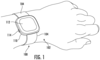
FIG. 1 depicts a wearable device according to some implementations of the present disclosure. -
FIG. 2 depicts a conductive housing of a wearable device according to some implementations of the present disclosure. -
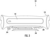
FIG. 3 depicts a side view of a wearable device with a bottom cover of a housing assembly of the wearable device removed according to some implementations of the present disclosure. -
FIG. 4 depicts the side view of a wearable device with a housing assembly of the wearable device removed according to some implementations of the present disclosure. -
FIG. 5 depicts a printed circuit board positioned within a conductive housing of a wearable device according to some implementations of the present disclosure. -
FIG. 6 depicts a printed circuit board of a wearable device according to some implementations of the present disclosure. -
FIG. 7 depicts a slot antenna defined by a gap between a conductive housing and a printed circuit board of a wearable device according to some implementations of the present disclosure. -
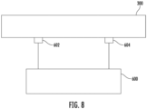
FIG. 8 depicts a parasitic element grounded to a printed circuit board of a wearable device according to some implementations of the present disclosure. -
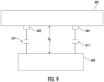
FIG. 9 depicts a parasitic element radio frequency grounded to a printed circuit board of a wearable device according to some implementations of the present disclosure. -
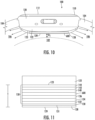
FIG. 10 depicts a side view of a wearable device including a parasitic element disposed between a film and a bottom cover of housing assembly according to some implementations of the present disclosure. -
FIG. 11 depicts a zoomed in cross-sectional view of the label, including the film and the parasitic element, and the bottom cover ofFIG. 10 according to some implementations of the present disclosure. -
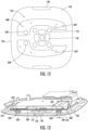
FIG. 12 depicts a top view of the label, including the film and the parasitic element ofFIG. 11 with the bottom cover removed according to some implementations of the present disclosure. -
FIG. 13 depicts a cross-sectional perspective view of a printed circuit board, a slot antenna, a bottom cover, a parasitic element, and a film of a wearable device according to some implementations of the present disclosure. -
FIG. 14 depicts a zoomed-in version ofFIG. 13 showing the slot antenna and opening in the bottom cover for connection of the parasitic element to the printed circuit board in more detail according to some implementations of the present disclosure. -
FIG. 15 depicts one configuration for mechanically connecting a parasitic element to a printed circuit board according to some implementations of the present disclosure. -
FIG. 16 depicts another configuration for mechanically connecting a parasitic element to a printed circuit board according to some implementations of the present disclosure. -
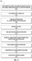
FIG. 17 depicts a method of assembling a wearable device that may include a film, a parasitic element, a plastic cover, a printed circuit board, a slot antenna, a conductive housing, and a display according to some implementations of the present disclosure. - Reference now will be made in detail to embodiments of the invention, one or more examples of which are illustrated in the drawings. Each example is provided by way of explanation of the invention, not limitation of the invention. In fact, it will be apparent to those skilled in the art that various modifications and variations can be made in the present invention without departing from the scope or spirit of the invention. For instance, features illustrated or described as part of one embodiment can be used with another embodiment to yield a still further embodiment. Thus, it is intended that the present invention covers such modifications and variations as come within the scope of the appended claims and their equivalents.
- As used herein, the terms "about," "approximately," or "generally," when used to modify a value, indicates that the value can be raised or lowered by 5% and remain within the disclosed embodiment. Further, when a plurality of ranges are provided, any combination of a minimum value and a maximum value described in the plurality of ranges are contemplated by the present invention. For example, if ranges of "from about 20% to about 80%" and "from about 30% to about 70%" are described, a range of "from about 20% to about 70%" or a range of "from about 30% to about 80%" are also contemplated by the present invention.
- Example aspects of the present disclosure are directed to a wearable device that can be worn, for instance, on a user's wrist or other location on the user's body. The wearable device can include an antenna, a conductive housing (e.g., a metal housing), a circuit board (e.g., a printed circuit board) located within the conductive housing, a cover (e.g., a plastic cover), and a label including film and a parasitic element. Further, although any type of antenna is contemplated by the present disclosure, it should be understood that, in some embodiments, the antenna can be a slot antenna defined by a gap (e.g., a 0.1 mm gap to about a 5 mm gap) between the conductive housing and the printed circuit board. The slot antenna can have a signal that operates at a plurality of different frequency bands. For example, the slot antenna can operate at one or more global navigation satellite system (GNSS) (e.g., global positioning system (GPS), GLONASS, Galileo, etc.) frequency bands. For instance, the one or more global navigation satellite system frequency bands can include one or more GPS frequency bands (e.g., 1164 MHz to 1189 MHz, 1563 MHz to 1587 MHz, 1215 MHz to 1240 MHz,). However, since the wearable device must be compact enough to be worn, for instance, on the user's wrist, the distance of the antenna from the user's wrist may be small, which can, in some circumstances, impact the performance (e.g., radiation efficiency) of the slot antenna at the one or more GPS frequency bands. Specifically, there can be a tendency for too much signal to radiate through the cover directly into the user's wrist, which can negatively affect GPS performance.
- It should also be understood that the antenna can operate at other frequency bands, such as those utilized in LTE, Wi-Fi, and Bluetooth applications as would be known to those of ordinary skill in the art.
- Regardless of the particular application for which the antenna of the wearable device is to be utilized, the wearable device includes a parasitic element. The parasitic element can be located or positioned between an outer surface of the cover and the film, where the film and parasitic element, as well as other layers, form a label. The parasitic element is placed as close to the user's wrist as possible in order to direct the RF (e.g., GPS) signal away from the wrist and out into the open air. The parasitic element is also metal-based (e.g., contains a conductive ink) and has a low resistance (e.g., less than about 1 Ohm across the length of the parasitic element). Further, the distance between the parasitic element and the user's wrist and the distance between the parasitic element and the system ground (e.g., the printed circuit board (PCB) of the device) are precisely controlled to be within certain ranges, because if the parasitic element were too close to the PCB, the parasitic element would not radiate efficiently at the desired frequency(ies) and not enhance the performance of the antenna. For instance, the distance D1 (see
FIG. 10 ) between the parasitic element and the user's wrist can range from about 0.15 millimeters to about 2.5 millimeters, such as from about 0.2 millimeters to about 2.25 millimeters, such as from about 0.25 millimeters to about 2 millimeters. Accordingly, the parasitic element is configured and arranged to be located at the distance D1 from the user's wrist when the wearable device is worn by the user. Meanwhile the distance D2 (seeFIG. 14 ) between the parasitic element and the system ground at thePCB 300 can range from about 1.25 millimeters to about 3.5 millimeters, such as from about 1.5 millimeters to about 3 millimeters, such as from about 1.75 millimeters to about 2.75 millimeters. - Additionally, the parasitic element can be applied as one of a series of layers that are printed onto to a film that surrounds the outer surface of the cover of the wearable device, thereby forming a label. The film (e.g., a transparent in molded label (IML) film), parasitic element, and other layers of the label can then be stamped, formed to the shape of the outer surface of the cover, and insert molded onto the outer surface of the cover to provide a thin design where the parasitic element is close to the user's wrist and further from the system ground (e.g., at PCB 300) to improve antenna performance. For instance, the label including the parasitic element can have a thickness T (see
FIG. 11 ) ranging from about 0.1 millimeters to about 0.5 millimeters, such as from about 0.125 millimeters to about 0.3 millimeters, such as from about 0.15 millimeters to about 0.25 millimeters. Further, the label can include a plurality of printed layers that can include, but may not be limited to, a decorative ink layer, a non-conductive making ink layer, a first gloss layer, a first insulating ink layer, a conductive ink layer, a second insulating ink layer, a second gloss layer, and a bonding layer, where each layer described can itself include a plurality of layers. The decorative ink layer is visible from the exterior of the wearable device through the transparent film, and the masking ink layer is utilized to hide the other layers of the label, such as the conductive ink layer that forms the parasitic element. The insulating ink layer(s) can add electrical stability to the parasitic element, and the gloss ink layer(s) can protect the conductive ink layer and the decorative ink layer from hot plastic during the insert molding process in which the various layers of the label including the parasitic element are joined to a plastic bottom cover of the wearable device. Further, the bonding layer bonds the label to the exterior surface of the plastic cover. - Further, the parasitic element can be electrically connected to the printed circuit board. For instance, the parasitic element can be electrically connected to a ground plane of the printed circuit board. For instance, the parasitic element can be direct current (DC) grounded to the printed circuit board at a first location thereon. Additionally, the parasitic element can be DC grounded to the printed circuit board at a second location thereon. The first location and the second location can be spaced apart from one another along the printed circuit board. Furthermore, the printed circuit board can include a first fastener (e.g., spring clip, booster pin, compression spring, etc.) at the first location and a second fastener (e.g., spring clip, booster pin, compression spring, etc.) at the second location to couple the parasitic element to the printed circuit board via a first opening and a second opening at the first location and the second location, respectively. For example, a first contact of the parasitic element and/or a second contact of the parasitic element can be mechanically coupled and/or electrically coupled to the printed circuit board via the first fastener and the second fastener, respectively, rather than via a solder connection.
- The parasitic element can be radio frequency (RF) grounded to the printed circuit board at multiple different locations. In this manner, the antenna (e.g., a slot antenna) induces one or more electrical currents on the parasitic element when operating at the one or more frequency bands, which can improve performance (e.g., radiation efficiency) of the antenna at the one or more frequency bands. Further, the parasitic element can improve the radiation efficiency of the antenna at the one or more frequency bands by at least about 2 decibels, such as by at least about 3 decibels, such as by at least about 4 decibels.
- The parasitic element can be electrically grounded to the printed circuit board. For instance, in some implementations, the parasitic element can be RF grounded to the printed circuit board multiple locations. In this manner, the antenna (e.g., a slot antenna) induces one or more electrical currents on the parasitic element when operating at the one or more frequency bands, which can improve performance (e.g., radiation efficiency) of the antenna at the one or more frequency bands. Further, the parasitic element can improve the radiation efficiency of the antenna at the one or more frequency bands by at least about 2 decibels, such as by at least about 3 decibels, such as by at least about 4 decibels.
- In some implementations, the parasitic element can be electrically grounded to the printed circuit board via a matching circuit. It should be understood that the matching circuit can include various electronic components (e.g., capacitors, inductors, resistors, switching devices, etc.) to facilitate electrically grounding the parasitic element to the printed circuit board. In alternative implementations, the parasitic element can be direct current (DC) grounded to the printed circuit board.
- Referring now to the FIGS.,
FIG. 1 depicts awearable device 100 according to some implementations of the present disclosure. As shown, thewearable device 100 can be worn, for instance, on awrist 102 of a user. For instance, thewearable device 100 can include aband 104 and ahousing assembly 110. Thehousing assembly 110 can be coupled to theband 104. In this manner, theband 104 can be fastened to thewrist 102 of the user to secure thehousing assembly 110 to thewrist 102 of the user. - In some implementations, the
wearable device 100 can include adisplay 112 that can display content (e.g., time, date, etc.) to the user. In some implementations, thedisplay 112 can include an interactive display (e.g., touchscreen or touch-free). In such implementations, the user can interact with thewearable device 100 via thedisplay 112 to control operation of thewearable device 100. Alternatively, or additionally, thewearable device 100 can include one ormore input devices 114 that can be manipulated by the user to interact with thewearable device 100. For instance, the one ormore input devices 114 can include a mechanical button that can be manipulated (e.g., pressed) to interact with thewearable device 100. In some implementations, the one ormore input devices 114 can be manipulated to control operation of a backlight (not shown) associated with thedisplay 112. It should be understood that the one ormore input devices 114 can be configured to allow the user to interact with thewearable device 100 in any suitable manner. For instance, in some implementations, the one ormore input devices 114 can be manipulated by the user to navigate through one or more menus on thedisplay 112. - In some implementations, the
wearable device 100 can be designed to be worn (e.g., continuously) by the user. When worn, thewearable device 100 can gather data regarding activities performed by the user, or regarding the user's physiological state. Such data may include data representative of the ambient environment around the user or the user's interaction with the environment. For example, the data can include motion data regarding the user's movements, ambient light, ambient noise, air quality, etc., and/or physiological data obtained by measuring various physiological characteristics of the user, such as heart rate, perspiration levels, body temperature, and the like. - Referring now to
FIG. 2 , a side view of thehousing assembly 110 of thewearable device 100 is provided according to some implementations of the present disclosure. As shown, thehousing assembly 110 can include aconductive housing 120. Theconductive housing 120 can be attached to theband 104 that is used to secure thehousing assembly 110 to the wrist 102 (FIG. 1 ) of the user. Thehousing assembly 110 can include abottom cover 122 coupled to theconductive housing 120. In some implementations, thebottom cover 122 can be coupled to the bottom of theconductive housing 120. In this manner, thebottom cover 122 can contact (e.g., touch) the wrist 102 (FIG. 1 ) of the user when thehousing assembly 110 is secured to thewrist 102 of the user via theband 104. - The
conductive housing 120 can include any suitable conductive material. For instance, in some implementations, theconductive housing 120 can include a metal housing. Thebottom cover 122 can include an insulating material. For instance, in some implementations, thebottom cover 122 can include a plastic cover. - In some implementations, the
wearable device 100 can include an electrocardiogram (ECG)electrode 200. As shown, theECG electrode 200 can be positioned within an opening (e.g., cutout) defined by thebottom cover 122. In this manner, theECG electrode 200 can be positioned adjacent the wrist 102 (FIG. 1 ) of the user when thehousing assembly 110 is secured to thewrist 102 of the user via theband 104. When theECG electrode 200 is in sufficient proximity to thewrist 102 of the user, theECG electrode 200 can be electrically connected to thewrist 102 of the user. Furthermore, it should be understood that thewearable device 100 can determine one or more health metrics (e.g., heart rate) of the user based, at least in part, on data obtained via theECG electrode 200 when theECG electrode 200 is electrically connected to thewrist 102 of the user. - Referring now to
FIGS. 3 and4 , a side view of thewearable device 100 is provided according to some implementations.FIG. 3 depicts a side view of thewearable device 100 with the bottom cover 122 (FIG. 2 ) removed.FIG. 4 depicts a side view of thewearable device 100 with the housing assembly 110 (FIG. 2 ) removed. As shown, thedisplay 112 can, in some implementations, include display traces (e.g., ITO coating) 116 and touch traces (e.g., ITO coating) 118. Thewearable device 100 can also include one ormore electrodes 124 to collect and store data regarding any number of parameters (electrodermal activity, etc.) that can be communicated to the user. - The
wearable device 100 can include a printedcircuit board 300 disposed within the housing assembly 110 (seeFIG. 2 ). For instance, in some implementations, a first portion of the printedcircuit board 300 can be positioned within theconductive housing 120 and a second portion of the printedcircuit board 300 can be positioned within the bottom cover 122 (seeFIG. 2 ). The printedcircuit board 300 can include a plurality of electronic components (not shown) disposed thereon. In some implementations, the printedcircuit board 300 can include a shielding can 302 covering at least a portion of the printedcircuit board 300. In this manner, the shielding can 302 can cover one or more electronic components of the plurality of electronic components disposed on the printedcircuit board 300. Alternatively, or additionally, the printedcircuit board 300 can include one or more charging pins 304. In this manner, thewearable device 100 can be coupled to a charging circuit (not shown) via the one or more charging pins 304 to facilitate charging of an energy storage device (e.g., battery) of thewearable device 100. - In some implementations, the
conductive housing 120 can define an opening (e.g., cutout) for one ormore electrodes 124. In this manner, the one ormore electrodes 124 can be visible to the user. In some implementations, the one ormore electrodes 124 can include an electrodermal activity (EDA) electrode. In such implementations, the user can contact (e.g., touch) the one ormore electrodes 124 to facilitate measuring one or more health metrics (e.g., heart-rate, blood pressure,, EDA etc.) of the user. It should be understood that the one ormore electrodes 124 can be electrically coupled to the printedcircuit board 300. - Referring now to
FIG. 5 , the printedcircuit board 300 can be positioned relative to theconductive housing 120 such that agap 400 is defined between theconductive housing 120 and the printedcircuit board 300. Thegap 400 can extend around a portion of or the entire perimeter of the printedcircuit board 300. Stated another way, at least some portion of the printedcircuit board 300 cannot contact (e.g., touch) theconductive housing 120. - In some implementations, a
width 402 of thegap 400 defined between theconductive housing 120 and the printedcircuit board 300 can range from about 0.5 millimeters to about 10 millimeters, such as from about 1 millimeter to about 7.5 millimeters, such as from about 1.5 millimeters to about 5 millimeters. In some implementations, thewidth 402 of thegap 400 can vary around the perimeter of the printedcircuit board 300. For instance, thewidth 402 of thegap 400 between theconductive housing 120 and the printedcircuit board 300 at a first portion of the perimeter of the printedcircuit board 300 can be different (e.g., wider, narrower) than thewidth 402 of thegap 400 between theconductive housing 120 and the printedcircuit board 300 at a second portion of the perimeter of the printedcircuit board 300. In some implementations the printedcircuit board 300 can touch theconductive housing 120. - Referring now to
FIGS. 6 and7 , the perimeter of the printedcircuit board 300 can, in some implementations, include a copper free or ground keep-outregion 306. It should be understood that the ground keep-outregion 306 can include a region of the printedcircuit board 300 where electronic components (e.g., resistors, capacitors, etc.) cannot be placed. In some implementations, awidth 308 of the ground keep-outregion 306 of the printedcircuit board 300 can range from 0.1 millimeters to about 2 millimeters, such as from about 0.2 millimeters to about 1.9 millimeters, such as from about 0.3 millimeters to about 1.8 millimeters. As will be discussed below, the ground keep-outregion 306 can act as an electrical gap. In some implementations, the ground keep-outregion 306 will be around the entire perimeter of the printedcircuit board 300. In some implementations the ground keep-outregion 306 will only be around a portion of the perimeter of the printedcircuit board 300. - In some implementations, an antenna, such as a slot antenna 500 (denoted by dashed line) can be defined by the
gap 400 between theconductive housing 120 and the printedcircuit board 300. Furthermore, in some implementations, theantenna 500 can be further defined by an electrical gap that spans thewidth 308 of the ground keep-outregion 306 of the printedcircuit board 300. In such implementations, the width of theslot antenna 500 can span the width 402 (FIG. 5 ) of thegap 400 and thewidth 308 of the ground keep-outregion 306 of the printedcircuit board 300. For instance, in some implementations, the width of theslot antenna 500 can range from about 0.5 millimeters to about 10 millimeters, such as from about 0.75 millimeters to about 9 millimeters, such as from about 1 millimeters to about 8 millimeters. - The
slot antenna 500 can be operable at a plurality of different frequency bands. For instance, theslot antenna 500 can be operable at one or more Global Navigation Satellite System (GNSS) frequency bands. In some implementations, the one or more GNSS frequency bands can include one or more GPS frequency bands. The one or more GPS frequency bands can include at least one of a first GPS frequency band ranging from about 1164 Megahertz (MHz) to about 1189 MHz, a second GPS frequency band ranging from about 1563 MHz to about 1587 MHz, and a third GPS frequency band ranging from about 1215 MHz to about 1240 MHz. Furthermore, in addition to the one or more GPS frequency bands, theantenna 500 can be configured to radiate at one or more frequency bands associated with cellular communications (e.g., 4G, 5G) or wireless local area communications (e.g., Wi-Fi or personal area networks (e.g., Bluetooth)). It should be understood however that theslot antenna 500 can be operable at frequency bands associated with any suitable communication standard. - In some implementations, the
slot antenna 500 can include afirst grounding contact 502 and asecond grounding contact 504. Thefirst grounding contact 502 can couple theconductive housing 120 to the ground of the printedcircuit board 300 at a first location. Conversely, thesecond grounding contact 504 can couple theconductive housing 120 to the ground of the printedcircuit board 300 at a second location. In some implementations, the first location and the second location can correspond to opposing sides of the printedcircuit board 300. It should be understood however that thefirst grounding contact 502 and thesecond grounding contact 504 can be coupled to the ground of the printedcircuit board 300 at any suitable location to adjust a length of theslot antenna 500. For instance, thefirst grounding contact 502 and thesecond grounding contact 504 can be positioned to shorten theslot antenna 500. Alternatively, thefirst grounding contact 502 and thesecond grounding contact 504 can be positioned to lengthen theslot antenna 500. - Referring now to
FIGS. 8 and9 , aparasitic element 600 of a wearable device (e.g.,wearable device 100 ofFIG. 1 ) is provided according to some implementations of the present disclosure. Theparasitic element 600 can be configured to increase the radiation of the RF signal when thewearable device 100 is on the user's wrist. In some implementations, theparasitic element 600 can be disposed entirely within the housing assembly 110 (FIG. 1 ) of thewearable device 100. In alternative implementations, theparasitic element 600 can be partially positioned within thehousing assembly 110. For instance, a first portion of theparasitic element 600 can be positioned within thehousing assembly 110, whereas a second portion of theparasitic element 600 can be positioned outside of thehousing assembly 110. - The
parasitic element 600 can be electrically connected to the printedcircuit board 300. For instance, theparasitic element 600 can be electrically connected to a ground plane of the printedcircuit board 300. In some implementations, theparasitic element 600 can be DC grounded to the printedcircuit board 300 at multiple locations. For instance, theparasitic element 600 can be DC grounded to the printedcircuit board 300 at afirst location 602 thereon and asecond location 604 thereon. As shown, thefirst location 602 and thesecond location 604 can be spaced apart from one another along the printedcircuit board 300. It should be understood that, in some implementations, theparasitic element 600 can be DC grounded to the printedcircuit board 300 at more than two locations (e.g.,first location 602, second location 604) thereon. - In some implementations, the
parasitic element 600 can be coupled to the printedcircuit board 300 via one or more matching circuits. For instance, in some implementations theparasitic element 600 can be RF grounded to the printedcircuit board 300 at thefirst location 602 thereon via a firstRF bypass capacitor 610. Additionally, theparasitic element 600 can be RF grounded to the printedcircuit board 300 at thesecond location 604 thereon via a secondRF bypass capacitor 612. It should be understood that the RF bypass capacitors (e.g., firstRF bypass capacitor 610 and second RF bypass capacitor 612) can leave theparasitic element 600 electrically isolated to electrical ground at direct current and low frequencies (e.g., non-RF frequencies). In some implementations, theparasitic element 600 can be coupled to the printed circuit board at thefirst location 602 through a first matching circuit that can consist of one or more inductors and capacitors. Additionally, theparasitic element 600 can be coupled to the printedcircuit board 300 at thesecond location 604 through a second matching circuit that can consist of one or more inductors and capacitors. - The
parasitic element 600 can improve performance (e.g., radiation efficiency) of theslot antenna 500 at the one or more frequency bands. For instance, since theparasitic element 600 is electrically coupled (e.g., radio frequency grounded, DC grounded) to the printedcircuit board 300 at multiple locations (e.g.,first location 602, second location 604), theslot antenna 500 can induce one or more electrical currents on theparasitic element 600 when theslot antenna 500 is operating at the one or more frequency bands. It should be understood that theslot antenna 500 inducing one or more electrical currents on theparasitic element 600 can improve performance (e.g., radiation efficiency) of theslot antenna 500 at the one or more frequency bands. For instance, in some implementations, the radiation efficiency of theantenna 500 can increase by at least 2 decibels, such as by at least about 3 decibels, such as at least by about 4 decibels due, at least in part, to theparasitic element 600 being electrically coupled to the printedcircuit board 300 at multiple locations (e.g.,first location 602, second location 604). - In some implementations, the printed
circuit board 300 can include a first fastener (e.g., spring clip) at thefirst location 602 thereon and a second fastener at the second location thereon. In this manner, theparasitic element 600 can be mechanically coupled to the printedcircuit board 300 at thefirst location 602 and thesecond location 604 via the first fastener and the second fastener, respectively, as discussed in more detail below. - Referring now to
FIG. 10 , a cross-sectional view of thewearable device 100 according to some implementations of the present disclosure is shown. Thewearable device 100 includes aparasitic element 600 which forms one layer of thelabel 150 and is disposed between afilm 128 and abottom cover 122 of ahousing assembly 110 according to some implementations of the present disclosure. Specifically, theparasitic element 600 can be disposed between anouter surface 123 of thebottom cover 122, which can be formed from a plastic material, and thefilm 128. Further, thebottom cover 122 is coupled to aconductive housing 120, which can be attached to theband 104 that is used to secure thehousing assembly 110 to thewrist 102 the user. The parasitic element is positioned a distance D1 away from the user'swrist 102. The distance D1 between theparasitic element 600 and the user'swrist 102 can range from about 0.15 millimeters to about 2.5 millimeters, such as from about 0.2 millimeters to about 2.25 millimeters, such as from about 0.25 millimeters to about 2 millimeters in order to improve the radiation efficiency of theslot antenna 500 of thewearable device 100. - Referring now to
FIG. 11 , a zoomed in cross-sectional view of thebottom cover 122 ofFIG. 10 and thelabel 150 which includes thefilm 128, theparasitic element 600, as well as additional layers. The label (e.g., in mold label (IML)) 150 can be insert molded onto theouter surface 123 of thebottom cover 122 as shown after various additional layers and theparasitic element 600 have been printed or otherwise applied to thefilm 128. The overall thickness T of thelabel 150, which includes thefilm 128, theparasitic element 600 and additional layers, can range from about 0.1 millimeters to about 0.5 millimeters, such as from about 0.125 millimeters to about 0.3 millimeters, such as from about 0.15 millimeters to about 0.25 millimeters. - Each layer of the
label 150 will now be discussed in more detail, where it is to be understood that each layer described hereafter can itself include more than one layer, such as 2 or more layers, such as 3 more layers, such as 4 or more layers. In some embodiments, each layer can be comprised of 2 to 10 layers, while in other embodiments, each layer may include only 1 individual layer. Further, the overall resistance across the length of theparasitic element 600 can be less than about 2.5 Ohms, such as less than about 1.5 Ohms, such as less than about 1 Ohm. - To form the
label 150, first, adecorative ink layer 130 can be applied to thefilm 128. Because thefilm 128 is transparent, thedecorative ink layer 130 can be visible to a user or viewer from thebottom 129 of thewearable device 100. It should be understood that thedecorative ink layer 130 may only be printed or applied to a portion of thefilm 128 depending on the particular designs, text, etc. that it is desired for a user or other viewer of thewearable device 100 to see. Any suitable ink of any desired color can be used for thedecorative ink layer 130, with the understanding that thedecorative ink layer 130 is non-conductive. - Next, a non-conductive
masking ink layer 132 can be applied on top of thedecorative ink layer 130. The non-conductivemasking ink layer 132 can be used to mask, hide, or obscure the other layers discussed below from the user or any other viewers of the bottom 129 of thewearable device 100, where such masking can enhance or highlight thedecorative ink layer 130. Further, the non-conductivemasking ink layer 132 may not be applied on top of the entireinner surface 131 of thefilm 128 and intervening layers because, as discussed in more detail below, various openings 125 (seeFIG. 12 ) may be needed for facilitating external charging of thewearable device 100 or where openings 126 (seeFIG. 12 ) may need to be exposed wheresensors 127 may be placed (seeFIGs. 12-14 ). The non-conductivemasking ink layer 132 can be any suitable color, so long as the non-conductivemasking ink layer 132 hides the layers that may be printed or applied on top of it. In some embodiments, the non-conductivemasking ink layer 132 is black, although it is to be understood that the color of the non-conductivemasking ink layer 132 is not limited to black. - Further, a
first gloss layer 134 can be applied on top of the non-conductivemasking ink layer 132. In one particular embodiment, thefirst gloss layer 134 can include four separate gloss layers. Thefirst gloss layer 134 can be used to protect any of the various layers of thelabel 150 from heat damage when thelabel 150 is applied to thebottom cover 122 via insert molding. In some embodiments, thefirst gloss layer 134 can be completely transparent. Additionally, thefirst gloss layer 134 may not be applied on top of the entireinner surface 131 of thefilm 128 and any intervening layers because, as discussed in more detail below,various openings 125 may be needed for facilitating external charging of thewearable device 100 or whereopenings 126 may be needed to be expose wheresensors 127 may be placed (seeFIGs. 12-14 ). - Next, a first insulating
ink layer 136 can be applied on top of thefirst gloss layer 134. The first insulating ink layer 136 (as well as the second insulatingink layer 140 discussed below) can be used to sandwich and protect theparasitic element 600, which is a conductive ink layer or layers, from interference with the other layers of thelabel 150. The first insulatingink layer 136 can be a dielectric ink. In some embodiments, the first insulatingink layer 136 can be completely transparent. Further, the first insulatingink layer 136 can include from about 40 wt.% to about 90 wt.%, such as from about 45 wt.% to about 85 wt.%, such as from about 50 wt.% to about 50 wt.% of a glycol ether based on the total weight of the first insulatingink layer 136. In one embodiment, the glycol ether can be diethylene glycol ethyl acetate, although it should be understood that any other suitable glycol ethers can be used as known to one of ordinary skill in the art. Additionally, the first insulatingink layer 136 may not be applied on top of the entireinner surface 131 of thefilm 128 and any intervening layers because, as discussed in more detail below,various openings 125 may be needed for facilitating external charging of thewearable device 100 or whereopenings 126 may be needed to be expose wheresensors 127 may be placed (seeFIGs. 12-14 ). - After the first insulating
ink layer 136 is applied, a conductive ink layer that forms theparasitic element 600 can be applied thereon. The conductive ink layer can be metallic and serves as theparasitic element 600 that facilitates the enhancement of theslot antenna 500 of thewearable device 100 resulting in stronger RF signals 106. In one particular embodiment, the conductive ink layer that forms theparasitic element 600 can include two separate conductive ink layers. The conductive ink layer can be a metallic paste. For instance, the conductive ink layer can include silver, copper, gold, aluminum, cobalt, nickel, tungsten, zinc, rhodium, iridium, ruthenium, osmium, palladium, platinum, or a combination thereof. However, it is also to be understood that non-metallic materials that are conductive can also be used. For example, the conductive ink layer can be in the form of a graphite paste in some embodiments. The metallic or conductive non-metallic material can be present in the conductive ink layer in an amount ranging from about 40 wt.% to about 85 wt.%, such as from about 45 wt.% to about 80 wt.%, such as from about 50 wt.% to about 75 wt.% based on the total weight of the conductive ink layer. The conductive ink layer can also include a polyester resin, an ethoxyline resin, an amorphous silica, or a combination thereof. The polyester resin can be present in an amount ranging from about 1 wt.% to about 25 wt.%, such as from about 2.5 wt.% to about 20 wt.%, such as from about 5 wt.% to about 15 wt.% based on the total weight of the conductive ink layer. Further, the ethoxyline resin can be present in an amount ranging from about 0.05 wt.% to about 5 wt.%, such as from about 0.075 wt.% to about 4 wt.%, such as from about 0.1 wt.% to about 3 wt.% based on the total weight of the conductive ink layer. Additionally, the conductive ink layer may not be applied on top of the entireinner surface 131 of thefilm 128 and any intervening layers because, as discussed in more detail below,various openings 125 may be needed for facilitating external charging of thewearable device 100 or whereopenings 126 may be needed to be expose wheresensors 127 may be placed (seeFIGs. 12-14 ). - In addition, a second insulating
ink layer 140 can be applied on top of the conductive ink layer that forms theparasitic element 600. The second insulating ink layer 140 (as well as the first insulatingink layer 136 discussed above) can be used to sandwich and protect the conductive ink layer forming theparasitic element 600 from interference with the other layers of thelabel 150. The secondinsulating ink layer 140 can be a dielectric ink. In some embodiments, the second insulatingink layer 140 can be completely transparent. Further, the second insulatingink layer 140 can include from about 40 wt.% to about 90 wt.%, such as from about 45 wt.% to about 85 wt.%, such as from about 50 wt.% to about 50 wt.% of a glycol ether. In one embodiment, the glycol ether can be diethylene glycol ethyl acetate, although it should be understood that any other suitable glycol ethers can be used as known to one of ordinary skill in the art. Additionally, the second insulatingink layer 140 may not be applied on top of the entireinner surface 131 of thefilm 128 and any intervening layers because, as discussed in more detail below,various openings 125 may be needed for facilitating external charging of thewearable device 100 or whereopenings 126 may be needed to be expose wheresensors 127 may be placed (seeFIGs. 12-14 ). Moreover, the second insulatingink layer 140 may not be applied over a portion of the conductive ink layer so that the resistance of theparasitic element 600 can be measured at one or moreexposed sections 624 after injection molding of thebottom cover 122 and prior to final assembly of thewearable device 100 and so that the conductive ink layer forming theparasitic element 600 can be connected to the printedcircuit board 300 at one or more exposed sections 626 (seeFIG. 12 ). - Additionally, a
second gloss layer 142 can be applied on top of the second insulatingink layer 140. In one particular embodiment, the second gloss can include two separate gloss layers. Thesecond gloss layer 142 can be used to protect any of the various layers of thelabel 150 from heat damage when thelabel 150 is applied to thebottom cover 122 via insert molding. In some embodiments, thesecond gloss layer 142 is completely transparent. Further, thesecond gloss layer 142 may not be applied on top of the entireinner surface 131 of thefilm 128 and any intervening layers because, as discussed in more detail below,various openings 125 may be needed for facilitating external charging of thewearable device 100 or whereopenings 126 may be needed to be expose wheresensors 127 may be placed (seeFIG. 12 ). Moreover, thesecond gloss layer 142 may not be applied over a portion of the conductive ink layer and any intervening layers so that the resistance of theparasitic element 600 can be measured at one or moreexposed sections 624 after injection molding of thebottom cover 122 and prior to final assembly of thewearable device 100 and so that the conductive ink layer forming theparasitic element 600 can be connected to the printedcircuit board 300 at one or more exposed sections 626 (seeFIG. 12 ). - Next, a
bonding layer 144 can be applied on top of thesecond gloss layer 142. Thebonding layer 144 can be used to enhance the adhesion of thelabel 150 to theouter surface 123 of thebottom cover 122 during the insert molding process. Further, it is to be understood that thebonding layer 144 may not be applied on top of the entireinner surface 131 of thefilm 128 and any intervening layers because, as discussed in more detail below,various openings 125 may be needed for facilitating external charging of thewearable device 100 or whereopenings 126 may be needed to be expose wheresensors 127 may be placed (seeFIGs. 12-14 ). Moreover, thebonding layer 144 may not be applied over a portion of the conductive ink layer and any intervening layers so that the resistance of theparasitic element 600 can be measured at one or moreexposed sections 624 after injection molding of theplastic cover 122 and prior to final assembly of thewearable device 100 and so that the conductive ink layer forming theparasitic element 600 can be electrically connected to the printedcircuit board 300 at one or more exposed sections 626 (seeFIG. 12 ). - Turning now to
FIG. 12 , a top view of thelabel 150, which includes thefilm 128 andparasitic element 600 ofFIG. 11 with thebottom cover 122 removed according to some implementations of the present disclosure is shown. As shown, the conductive ink layer forming theparasitic element 600 can include one or moreexposed sections 624 that are free of the second insulatinglayer 140, thesecond gloss layer 142, and thebonding layer 144 so that the resistance of theparasitic element 600 can be measured after injection molding of thebottom cover 122 and prior to assembly of thewearable device 100. Further, as shown, the conductive ink layer forming theparasitic element 600 can include one or moreexposed sections 626 that are free of the second insulatinglayer 140, thesecond gloss layer 142, and thebonding layer 144 so that theparasitic element 600 can be electrically connected to the printedcircuit board 300 viaopenings 620 in the bottom cover 122 (seeFIGs. 13-14 ). - Referring still to
FIG. 12 , the arrangement of theparasitic element 600 on thecover 122 is discussed in more detail. In particular, the configuration of theparasitic element 600 may be selected to occupy a significant portion (20-80%) of thecover 122, and, in turn, the biosensor hub of thewearable device 100. While not limited to any specific shape, the shape of theparasitic element 600 can be driven by other factors such as the location of the sensors 127 (e.g., heart rate monitor sensors), or location of the injection molding gates used to form thecover 122. The shape of theparasitic element 600 can be selected to balance achieving a larger surface area while also maximizing the clearance to the nearest metal parts of the wearable device (e.g., thePCB 300 or the conductive housing 120). As such, theparasitic element 600 generally does not extend to the edges of the cover 122 (and thus the edges of the biosensor hub of the wearable device 100) because that area is too close to theconductive housing 120. The largest dimensions of theparasitic element 600 are generally between about 1/10 of a wavelength to about 1/2 of a wavelength of the lowest frequency that is being boosted by theparasitic element 600. Further, it is to be understood that there could be multipleparasitic elements 600 printed or otherwise disposed on thefilm 128 to form thelabel 150. In other words, thelabel 150 can include one or moreparasitic elements 600, such as 2, 3, 4, 5, 6, or moreparasitic elements 600, where it is to be understood that the number ofparasitic elements 600 could match up to the number ofopenings 620 in thebottom cover 122 for connection of theparasitic element 600 to the printedcircuit board 300 via any desirable fastener or contact (e.g., spring clip 614 andbooster pin 616,compression spring 618, etc. as shown inFIGs. 13-16 ). - Turning now to
FIGs. 13-14 ,FIG. 13 depicts a cross-sectional perspective view of a printedcircuit board 300, aslot antenna 500, abottom cover 122, and alabel 150, which includes aparasitic element 600 and afilm 128, as well as the other various layers discussed above, of awearable device 100, andFIG. 14 is a zoomed-in view ofFIG. 13 showing theslot antenna 500 andopenings 620 in thebottom cover 122 for connection of theparasitic element 600 to the printedcircuit board 300 in more detail according to some implementations of the present disclosure. The distance D2 (seeFIG. 14 ) between theparasitic element 600 and theantenna 500 can range from about 1.25 millimeters to about 3.5 millimeters, such as from about 1.5 millimeters to about 3 millimeters, such as from about 1.75 millimeters to about 2.75 millimeters in order to optimize the GPS performance of thewearable device 100. Theopenings 620 in thebottom cover 122 are generally aligned with the exposedsections 626 of the conductive ink layer forming the parasitic element 600 (seeFIG. 12 ) for connecting theparasitic element 600 to the printedcircuit board 300. The diameter d of theopenings 620 can range from about 0.6 millimeters to about 1.2 millimeters, such as from about 0.7 millimeters to about 1.1 millimeters, such as from about 0.8 millimeters to about 1 millimeter. Without intending to be limited by any particular theory, the present inventors have found that such a diameter range preserves the strength and integrity of thefilm 128 while also ensuring that the mechanical connection between theparasitic element 600 and the printedcircuit board 300 is sufficient. Additionally,conductive pads 622 in the form of a glue, paste, foam, or other suitable medium can be applied to theparasitic element 600 such that theconductive pads 622 are aligned with theopenings 620 in thebottom cover 122 to enhance the mechanical connection of theparasitic element 600 to the printedcircuit board 300 via a fastener in the form of a spring clip 614 andbooster pin 616 or acompression spring 618 as discussed in more detail below (seeFIGs. 15-16 ). Further,conductive pads 623 in the form of a glue, paste, foam, or other suitable medium can be applied to the printedcircuit board 300 to also enhance the mechanical connection of theparasitic element 600 to the printedcircuit board 300 via a fastener in the form of a spring clip 614 andbooster pin 616, acompression spring 618, or any other suitable fastener as discussed in more detail below (seeFIGs. 15-16 ). - As mentioned above,
FIG. 15 depicts one configuration for mechanically connecting theparasitic element 600 to the printedcircuit board 300 according to some implementations of the present disclosure via a spring clip 614 and abooster pin 616, whereconductive pads booster pin 616 may be used when higher frequencies are required of theantenna 500 in the wearable device 100 (e.g., GPS applications). Further,FIG. 16 depicts another configuration for mechanically connecting theparasitic element 600 to the printedcircuit board 300 according to some implementations of the present disclosure via acompression spring 618. The inductance inherently present in thecompression spring 618 may be desired, for instance, in applications where lower frequencies are required of theantenna 500 in the wearable device (e.g., LTE applications). -
FIG. 17 depicts amethod 700 of assembling awearable device 100 that may include alabel 150, acover 122, a printedcircuit board 300, an antenna 500 (e.g., a slot antenna), aconductive housing 120, and adisplay 112 according to some implementations of the present disclosure. For instance, instep 702, one or more decorative ink layers 130, non-conductivemasking ink layers 132, gloss layers 134 and/or 142, insulating ink layers 136 and/or 140, and conductive ink layers forming aparasitic element 600 can be printed or otherwise applied onto afilm 128 to form thelabel 150. Then, instep 704, abonding layer 144 can be applied to thefilm 128 with the various layers printed or otherwise applied thereon. Next, instep 706, thelabel 150 can be formed into a desired shape (e.g., a shape that corresponds with the shape of theouter surface 123 of the bottom cover 122), after which anylabel 150 excess can be trimmed away instep 708. Thereafter, instep 710, thelabel 150 can be molded onto theouter surface 123 of thebottom cover 122, such as via insert molding. Next, instep 712, theparasitic element 600 that is a part of thelabel 150 can be mechanically connected to a printedcircuit board 300 that is positioned above thebottom cover 122. Next, instep 714, theconductive housing 120 can be attached to thebottom cover 122. Further, instep 716, theantenna 500 can be formed by thegap 400 around the printedcircuit board 300. Then, instep 718, thedisplay 112 can be attached to theconductive housing 120. Lastly, it should be understood that the steps of theabove method 700 can be performed in any other appropriate order as would be understood by one of ordinary skill in the art. - The proposed solution in particular relates to the following embodiments:
- Embodiment 1:
A wearable device comprising:- a printed circuit board;
- a conductive housing;
- an antenna;
- a cover having an outer surface; and
- a label comprising a film and a parasitic element, wherein the parasitic element is located between the film and the outer surface of the cover.
- Embodiment 2:
The wearable device of embodiment 1, wherein the parasitic element comprises a conductive ink layer. - Embodiment 3:
The wearable device of embodiment 1 or 2, wherein the label is insert molded onto the outer surface of the cover. - Embodiment 4:
The wearable device of any one of the embodiments 1 to 3, wherein the label comprises a decorative ink layer between the film and the parasitic element. - Embodiment 5:
The wearable device of embodiment 4, wherein the label comprises a non-conductive masking ink layer between the decorative ink layer and the parasitic element. - Embodiment 6:
The wearable device of embodiment 5, wherein the label comprises a first insulating ink layer. - Embodiment 7:
The wearable device of embodiment 6, wherein the label comprises a first gloss layer between the non-conductive masking ink layer and the first insulating ink layer. - Embodiment 8:
The wearable device of embodiment 6 or 7, wherein the label comprises a second insulating ink layer, wherein the parasitic element is between the first insulating ink layer and the second insulating ink layer. - Embodiment 9:
The wearable device of embodiment 8, wherein the label comprises a bonding layer, wherein the bonding layer connects the label to the outer surface of the cover. - Embodiment 10:
The wearable device of embodiment 9, wherein the label comprises a second gloss layer between the second insulating ink layer and the bonding layer. - Embodiment 11:
The wearable device of embodiment 1, wherein the antenna is a slot antenna defined by a gap between the printed circuit board and the conductive housing. - Embodiment 12:
A label for a wearable device containing an antenna, the label comprising multiple layers including a film, a decorative ink layer, a non-conductive masking ink layer, a first insulating ink layer, a parasitic element, and a second insulating ink layer, wherein the multiple layers of the label are applied onto the film, further wherein the parasitic element comprises a conductive ink layer. - Embodiment 13:
The label of embodiment 12, further comprising a bonding layer. - Embodiment 14:
The label of embodiment 12 or 13, further comprising a first gloss layer. - Embodiment 15:
The label of any one of embodiments 12 to 14, wherein a portion of the conductive ink layer is exposed and free of additional layers printed thereon. - Embodiment 16:
The label of any one of embodiments 12 to 15, wherein the label is configured for being joined to a plastic cover during an insert molding process. - Embodiment 17:
The label of any of the embodiments 1 to 16, wherein the parasitic element is electrically grounded to the printed circuit board via radio-frequency grounding, direct current grounding, or a matching circuit. - Embodiment 18:
A method of forming a label for a wearable device containing an antenna, the method comprising:- printing one or more layers of non-conductive masking ink onto a film;
- printing one or more layers of conductive ink onto the film to define a parasitic element;
- printing a bonding layer onto the film to form the label; and
- forming the label into a shape that matches a shape of a cover to which it is to be applied.
- Embodiment 19:
The method of embodiment 18, wherein the label is joined to an outer surface of the cover during an insert molding process, wherein the bonding layer joins the label to the cover. - Embodiment 20:
The method of embodiment 18 or 19, further comprising:
printing one or more layers of decorative ink onto the film. - Embodiment 21:
The method of any one of embodiments 18 to 20, further comprising:
printing one or more layers of insulating ink onto the film. - Embodiment 22:
The method of any one of embodiments 18 to 21, further comprising trimming the label to remove any excess. - While the present subject matter has been described in detail with respect to various specific example embodiments thereof, each example is provided by way of explanation, not limitation of the disclosure. Those skilled in the art, upon attaining an understanding of the foregoing, can readily produce alterations to, variations of, and equivalents to such embodiments. Accordingly, the subject disclosure does not preclude inclusion of such modifications, variations and/or additions to the present subject matter as would be readily apparent to one of ordinary skill in the art. For instance, features illustrated or described as part of one embodiment can be used with another embodiment to yield a still further embodiment. Thus, it is intended that the present disclosure cover such alterations, variations, and equivalents.
Claims (15)
- A wearable device to be worn on a wrist of a user, the wearable device comprising:a printed circuit board;a conductive housing;an antenna;a cover having an outer surface, wherein the cover is coupled to a bottom of the conductive housing and adapted to be in contact with the wrist of the user; anda label comprising a film and a parasitic element, wherein the parasitic element is located between the film and the outer surface of the cover.
- The wearable device of claim 1, wherein the label is configured to direct an antenna signal of the antenna away from the wrist of the user.
- The wearable device of claim 1, wherein the antenna is a slot antenna defined by a gap between the printed circuit board and the conductive housing.
- The wearable device of claim 1, wherein the parasitic element comprises a conductive ink layer.
- The wearable device of claim 1 or 4, wherein the label is insert molded onto the outer surface of the cover.
- The wearable device of any one of the preceding claims, wherein the label comprises a decorative ink layer between the film .and the parasitic element.
- The wearable device of claim 6, wherein the decorative ink layer is applied to the film or a portion of the film, wherein the film is transparent and the decorative ink layer is visible from an exterior of the wearable device through the film.
- The wearable device of claim 6, wherein the label comprises a non-conductive masking ink layer between the decorative ink layer and the parasitic element.
- The wearable device of claim 8, wherein the label comprises a first insulating ink layer.
- The wearable device of claim 9, wherein the label comprises a first gloss layer between the non-conductive masking ink layer and the first insulating ink layer.
- The wearable device of claim 9 or 10, wherein the label comprises a second insulating ink layer, wherein the parasitic element is between the first insulating ink layer and the second insulating ink layer.
- The wearable device of claim 11, wherein the label comprises a bonding layer, wherein the bonding layer connects the label to the outer surface of the cover.
- The wearable device of claim 12, wherein the label comprises a second gloss layer between the second insulating ink layer and the bonding layer.
- The wearable device of claim 11, wherein the film, the decorative ink layer, the non-conductive masking ink layer, the first insulating ink layer, the parasitic element, and the second insulating ink layer are applied onto the film.
- The wearable device of any of the preceding claims, wherein the parasitic element is electrically grounded to the printed circuit board via radio-frequency grounding, direct current grounding, or a matching circuit.
Priority Applications (1)
| Application Number | Priority Date | Filing Date | Title |
|---|---|---|---|
| EP25159708.4A EP4535570A3 (en) | 2022-05-19 | 2022-05-19 | Conductive ink-based parasitic element for a device antenna |
Applications Claiming Priority (3)
| Application Number | Priority Date | Filing Date | Title |
|---|---|---|---|
| PCT/CN2022/093823 WO2023221035A1 (en) | 2022-05-19 | 2022-05-19 | Conductive ink-based parasitic element for a device antenna |
| EP25159708.4A EP4535570A3 (en) | 2022-05-19 | 2022-05-19 | Conductive ink-based parasitic element for a device antenna |
| EP22888610.7A EP4298689A4 (en) | 2022-05-19 | 2022-05-19 | PARASITIC ELEMENT BASED ON CONDUCTIVE INK FOR AN ANTENNA DEVICE |
Related Parent Applications (1)
| Application Number | Title | Priority Date | Filing Date |
|---|---|---|---|
| EP22888610.7A Division EP4298689A4 (en) | 2022-05-19 | 2022-05-19 | PARASITIC ELEMENT BASED ON CONDUCTIVE INK FOR AN ANTENNA DEVICE |
Publications (2)
| Publication Number | Publication Date |
|---|---|
| EP4535570A2 true EP4535570A2 (en) | 2025-04-09 |
| EP4535570A3 EP4535570A3 (en) | 2025-06-18 |
Family
ID=88834279
Family Applications (2)
| Application Number | Title | Priority Date | Filing Date |
|---|---|---|---|
| EP22888610.7A Pending EP4298689A4 (en) | 2022-05-19 | 2022-05-19 | PARASITIC ELEMENT BASED ON CONDUCTIVE INK FOR AN ANTENNA DEVICE |
| EP25159708.4A Pending EP4535570A3 (en) | 2022-05-19 | 2022-05-19 | Conductive ink-based parasitic element for a device antenna |
Family Applications Before (1)
| Application Number | Title | Priority Date | Filing Date |
|---|---|---|---|
| EP22888610.7A Pending EP4298689A4 (en) | 2022-05-19 | 2022-05-19 | PARASITIC ELEMENT BASED ON CONDUCTIVE INK FOR AN ANTENNA DEVICE |
Country Status (7)
| Country | Link |
|---|---|
| US (1) | US12314795B2 (en) |
| EP (2) | EP4298689A4 (en) |
| JP (1) | JP2025517739A (en) |
| KR (1) | KR20250005242A (en) |
| CN (1) | CN119213628A (en) |
| TW (1) | TW202412385A (en) |
| WO (1) | WO2023221035A1 (en) |
Family Cites Families (20)
| Publication number | Priority date | Publication date | Assignee | Title |
|---|---|---|---|---|
| AU5917499A (en) * | 1998-09-11 | 2000-04-03 | Alexander Gelbman | Smart electronic label employing electronic ink |
| JP5101318B2 (en) * | 2008-01-28 | 2012-12-19 | グンゼ株式会社 | Drying apparatus and drying method |
| JP2010066045A (en) * | 2008-09-09 | 2010-03-25 | Casio Comput Co Ltd | Radio wave receiving system |
| US20100060459A1 (en) | 2008-09-11 | 2010-03-11 | IP B.V.Strawinskylaan | Rfid tag |
| FI20115072A0 (en) | 2011-01-25 | 2011-01-25 | Pulse Finland Oy | Multi-resonance antenna, antenna module and radio unit |
| JP5998795B2 (en) * | 2012-09-24 | 2016-09-28 | セイコーエプソン株式会社 | Electronic clock with built-in antenna |
| JP5907479B2 (en) * | 2013-03-22 | 2016-04-26 | カシオ計算機株式会社 | ANTENNA DEVICE AND ELECTRONIC DEVICE |
| CN105515599A (en) * | 2014-09-30 | 2016-04-20 | 深圳富泰宏精密工业有限公司 | Wireless communication device |
| JP6459593B2 (en) * | 2015-02-13 | 2019-01-30 | セイコーエプソン株式会社 | Antenna device and electronic timepiece |
| TWI659678B (en) | 2015-09-15 | 2019-05-11 | 大陸商東莞錢鋒特殊膠黏製品有限公司 | Antenna composite molding structure of mobile electronic device and manufacturing method thereof |
| CN205177994U (en) | 2015-11-06 | 2016-04-20 | 乐视移动智能信息技术(北京)有限公司 | Antenna system |
| WO2018016574A1 (en) * | 2016-07-20 | 2018-01-25 | シチズン時計株式会社 | Portable radio clock |
| US20180028072A1 (en) * | 2016-07-29 | 2018-02-01 | VivaLnk, Inc. | Wearable thermometer patch capable of measuring human skin temperature at high duty cycle |
| WO2018068190A1 (en) | 2016-10-10 | 2018-04-19 | 华为技术有限公司 | Wearable device |
| CN110036349B (en) * | 2017-02-16 | 2024-01-30 | 华为技术有限公司 | Wearable equipment |
| TWI645688B (en) * | 2017-07-11 | 2018-12-21 | 巨擘科技股份有限公司 | Wearable device and operating method thereof |
| TWI638485B (en) * | 2017-10-05 | 2018-10-11 | 廣達電腦股份有限公司 | Wearable device |
| US10992029B2 (en) * | 2018-12-13 | 2021-04-27 | Fitbit, Inc. | Multiple band antenna structures |
| CN114444643B (en) | 2019-04-17 | 2024-08-06 | 苹果公司 | Wireless locatable tags |
| US10839171B2 (en) | 2019-04-22 | 2020-11-17 | Apple Inc. | Integrated sensing tag-based wireless sensing within electronic devices |
-
2022
- 2022-05-19 JP JP2024568290A patent/JP2025517739A/en active Pending
- 2022-05-19 KR KR1020247037350A patent/KR20250005242A/en active Pending
- 2022-05-19 WO PCT/CN2022/093823 patent/WO2023221035A1/en not_active Ceased
- 2022-05-19 EP EP22888610.7A patent/EP4298689A4/en active Pending
- 2022-05-19 EP EP25159708.4A patent/EP4535570A3/en active Pending
- 2022-05-19 CN CN202280096054.5A patent/CN119213628A/en active Pending
- 2022-05-19 US US18/251,772 patent/US12314795B2/en active Active
-
2023
- 2023-05-05 TW TW112116716A patent/TW202412385A/en unknown
Also Published As
| Publication number | Publication date |
|---|---|
| EP4298689A4 (en) | 2024-05-29 |
| EP4535570A3 (en) | 2025-06-18 |
| US12314795B2 (en) | 2025-05-27 |
| US20240354546A1 (en) | 2024-10-24 |
| KR20250005242A (en) | 2025-01-09 |
| WO2023221035A1 (en) | 2023-11-23 |
| EP4298689A1 (en) | 2024-01-03 |
| TW202412385A (en) | 2024-03-16 |
| JP2025517739A (en) | 2025-06-10 |
| CN119213628A (en) | 2024-12-27 |
Similar Documents
| Publication | Publication Date | Title |
|---|---|---|
| TWI568329B (en) | Antenna structures with electrical connections to device housing members | |
| EP1451897B1 (en) | Vhf wave receiver antenna housed in a wristband of a portable electronic device | |
| US10461404B2 (en) | Terminal housing and terminal | |
| US8717240B2 (en) | Multi-angle ultra wideband antenna with surface mount technology | |
| US9152833B2 (en) | Antenna circuit | |
| JPH11177327A (en) | Inverse f antenna device | |
| EP4145631A1 (en) | Wearable device | |
| US12314795B2 (en) | Conductive ink-based parasitic element for a device antenna | |
| CN110994137A (en) | Wearable electronic device | |
| KR101643928B1 (en) | Antenna structure | |
| CN114488767A (en) | Wearable equipment and intelligent wrist-watch | |
| EP4338232B1 (en) | Wearable computing device having a multi-band slot antenna and a grounded parasitic element | |
| CN112886206B (en) | Wearable electronic device | |
| KR101651902B1 (en) | Manufacturing method of antenna structure | |
| JP5873350B2 (en) | Wireless module with integrated antenna | |
| CN112886212B (en) | Wearable electronic equipment | |
| FI20205799A1 (en) | A cover structure and a module for a miniaturized wearable rf-device and a wearable rf-device | |
| CN121125895A (en) | An electronic device | |
| CN109462418B (en) | Wearable device | |
| KR20170089482A (en) | Electronic device having wristwatch |
Legal Events
| Date | Code | Title | Description |
|---|---|---|---|
| PUAI | Public reference made under article 153(3) epc to a published international application that has entered the european phase |
Free format text: ORIGINAL CODE: 0009012 |
|
| STAA | Information on the status of an ep patent application or granted ep patent |
Free format text: STATUS: THE APPLICATION HAS BEEN PUBLISHED |
|
| AC | Divisional application: reference to earlier application |
Ref document number: 4298689 Country of ref document: EP Kind code of ref document: P |
|
| AK | Designated contracting states |
Kind code of ref document: A2 Designated state(s): AL AT BE BG CH CY CZ DE DK EE ES FI FR GB GR HR HU IE IS IT LI LT LU LV MC MK MT NL NO PL PT RO RS SE SI SK SM TR |
|
| REG | Reference to a national code |
Ref country code: DE Ref legal event code: R079 Free format text: PREVIOUS MAIN CLASS: H01Q0019100000 Ipc: H01Q0001270000 |
|
| PUAL | Search report despatched |
Free format text: ORIGINAL CODE: 0009013 |
|
| AK | Designated contracting states |
Kind code of ref document: A3 Designated state(s): AL AT BE BG CH CY CZ DE DK EE ES FI FR GB GR HR HU IE IS IT LI LT LU LV MC MK MT NL NO PL PT RO RS SE SI SK SM TR |
|
| RIC1 | Information provided on ipc code assigned before grant |
Ipc: H01Q 19/10 20060101ALI20250509BHEP Ipc: H01Q 13/10 20060101ALI20250509BHEP Ipc: H01Q 1/44 20060101ALI20250509BHEP Ipc: H01Q 1/27 20060101AFI20250509BHEP |
|
| STAA | Information on the status of an ep patent application or granted ep patent |
Free format text: STATUS: REQUEST FOR EXAMINATION WAS MADE |
|
| 17P | Request for examination filed |
Effective date: 20251217 |
|
| GRAP | Despatch of communication of intention to grant a patent |
Free format text: ORIGINAL CODE: EPIDOSNIGR1 |
|
| STAA | Information on the status of an ep patent application or granted ep patent |
Free format text: STATUS: GRANT OF PATENT IS INTENDED |
|
| INTG | Intention to grant announced |
Effective date: 20260226 |