JP5998795B2 - Electronic clock with built-in antenna - Google Patents
Electronic clock with built-in antenna Download PDFInfo
- Publication number
- JP5998795B2 JP5998795B2 JP2012209260A JP2012209260A JP5998795B2 JP 5998795 B2 JP5998795 B2 JP 5998795B2 JP 2012209260 A JP2012209260 A JP 2012209260A JP 2012209260 A JP2012209260 A JP 2012209260A JP 5998795 B2 JP5998795 B2 JP 5998795B2
- Authority
- JP
- Japan
- Prior art keywords
- antenna
- antenna body
- electronic timepiece
- clock
- feeding
- Prior art date
- Legal status (The legal status is an assumption and is not a legal conclusion. Google has not performed a legal analysis and makes no representation as to the accuracy of the status listed.)
- Expired - Fee Related
Links
Images


Classifications
-
- G—PHYSICS
- G04—HOROLOGY
- G04R—RADIO-CONTROLLED TIME-PIECES
- G04R60/00—Constructional details
- G04R60/06—Antennas attached to or integrated in clock or watch bodies
- G04R60/10—Antennas attached to or integrated in clock or watch bodies inside cases
-
- G—PHYSICS
- G01—MEASURING; TESTING
- G01S—RADIO DIRECTION-FINDING; RADIO NAVIGATION; DETERMINING DISTANCE OR VELOCITY BY USE OF RADIO WAVES; LOCATING OR PRESENCE-DETECTING BY USE OF THE REFLECTION OR RERADIATION OF RADIO WAVES; ANALOGOUS ARRANGEMENTS USING OTHER WAVES
- G01S19/00—Satellite radio beacon positioning systems; Determining position, velocity or attitude using signals transmitted by such systems
- G01S19/01—Satellite radio beacon positioning systems transmitting time-stamped messages, e.g. GPS [Global Positioning System], GLONASS [Global Orbiting Navigation Satellite System] or GALILEO
- G01S19/13—Receivers
- G01S19/14—Receivers specially adapted for specific applications
-
- H—ELECTRICITY
- H01—ELECTRIC ELEMENTS
- H01Q—ANTENNAS, i.e. RADIO AERIALS
- H01Q1/00—Details of, or arrangements associated with, antennas
- H01Q1/27—Adaptation for use in or on movable bodies
- H01Q1/273—Adaptation for carrying or wearing by persons or animals
-
- H—ELECTRICITY
- H01—ELECTRIC ELEMENTS
- H01Q—ANTENNAS, i.e. RADIO AERIALS
- H01Q1/00—Details of, or arrangements associated with, antennas
- H01Q1/44—Details of, or arrangements associated with, antennas using equipment having another main function to serve additionally as an antenna, e.g. means for giving an antenna an aesthetic aspect
-
- H—ELECTRICITY
- H01—ELECTRIC ELEMENTS
- H01Q—ANTENNAS, i.e. RADIO AERIALS
- H01Q7/00—Loop antennas with a substantially uniform current distribution around the loop and having a directional radiation pattern in a plane perpendicular to the plane of the loop
Landscapes
- Physics & Mathematics (AREA)
- General Physics & Mathematics (AREA)
- Engineering & Computer Science (AREA)
- Radar, Positioning & Navigation (AREA)
- Remote Sensing (AREA)
- Computer Networks & Wireless Communication (AREA)
- Electric Clocks (AREA)
- Electromechanical Clocks (AREA)
- Details Of Aerials (AREA)
- Support Of Aerials (AREA)
Description
本発明は、アンテナを内蔵したアンテナ内蔵式電子時計に関する。 The present invention relates to an electronic timepiece with a built-in antenna.
特許文献1には、電子腕時計において、時計ガラス5の下面にその外周に沿ってループ
状にアンテナ20を形成したことや、時計ケース1のうち12時及び6時の方向にバンド
取付部2を形成したことが開示されている。また、同文献1の図1には、一方のバンド取
付部2の近くにアンテナ20の電極21を設けたこと、すなわちアンテナ20の電極21
を12時又は6時の方向に設けたことが開示されている。
Patent Document 1 discloses that in an electronic wristwatch, an
Is provided in the direction of 12 o'clock or 6 o'clock.
また、特許文献2には、ループアンテナとして機能するアンテナ11を腕携帯型受信機
のケース17に一体的に配設したことが開示されており、同文献2の図1には、バンド4
1を係止するための突起部21をケース17の2箇所に形成し、一方の突起部21の近く
にアンテナ11の給電口15を設けたことが開示されている。
Patent Document 2 discloses that an
It is disclosed that protrusions 21 for locking 1 are formed at two places on the
ところで、GPS(Global Positioning System)衛星からの電波を屋内で受信するこ
とはできないので、電子腕時計では、装着者が屋外にいるときにGPS衛星からの電波を
受信することになる。屋外の場合、装着者は、腕時計をした腕を下げているかその手を身
体の前に位置させた姿勢でいることが多い。このような姿勢では時計表面の法線方向が水
平方向に向けられていることになる。例えば、円環状(O型形状)のループアンテナや、
円環の一部を切り欠いたC型形状のループアンテナでは、ループ面を含む平面における放
射指向性が円環の中心から見て給電用の電極が設けられた方向又はその付近で最大になる
。従って、特許文献1,2に開示されたループアンテナでは、装着者が腕時計をした腕を
下げているかその手を身体の前に位置させている場合に、アンテナ利得の最も大きい最大
放射方向が、バンドと平行な方向、すなわち天頂方向ではなく水平方向に向けられている
ため、受信性能が十分に発揮できていなかった。
By the way, since the radio wave from the GPS (Global Positioning System) satellite cannot be received indoors, the electronic wristwatch receives the radio wave from the GPS satellite when the wearer is outdoors. When outdoors, the wearer is often in a posture with the wrist of the wrist watch lowered or with the hand positioned in front of the body. In such an attitude, the normal direction of the watch surface is oriented in the horizontal direction. For example, an annular (O-shaped) loop antenna,
In a C-shaped loop antenna in which a part of the ring is cut out, the radiation directivity in a plane including the loop surface is maximized in or near the direction in which the feeding electrode is provided as viewed from the center of the ring. . Therefore, in the loop antenna disclosed in Patent Documents 1 and 2, when the wearer is lowering the wrist arm or the hand is positioned in front of the body, the maximum radiation direction with the largest antenna gain is Since it is directed in the direction parallel to the band, that is, in the horizontal direction, not the zenith direction, the reception performance could not be sufficiently exhibited.
本発明は、上述した事情に鑑みてなされたものであり、十分な受信性能を維持しつつア
ンテナを小型化することが可能なアンテナ内蔵式電子時計を提供することを解決課題とす
る。
The present invention has been made in view of the circumstances described above, and an object of the present invention is to provide an electronic timepiece with a built-in antenna that can reduce the size of the antenna while maintaining sufficient reception performance.
以上の課題を解決するため、本発明は、外装ケースと、前記外装ケースに収納された環
状のアンテナ体と、前記外装ケースに収納され、時刻を表示する時刻表示部と、を備えた
アンテナ内蔵式電子時計において、前記アンテナ体は、環状の誘電体と、前記誘電体上に
設けられ、環状の一部を切り欠いた形状を有し、所定の電位が給電される導電性の給電素
子と、前記誘電体上に前記給電素子と離間して設けられ、環状又は環状の一部を切り欠い
た形状を有する導電性の無給電素子と、を備え、前記給電素子には、前記所定の電位が給
電される給電位置が一箇所設けられ、前記給電位置は、当該アンテナ内蔵式電子時計を平
面視したとき、当該アンテナ内蔵式電子時計の中心から見て8時の方向から10時の方向
までの範囲に設けられている、ことを特徴とする。
In order to solve the above-described problems, the present invention includes an external case, an annular antenna body accommodated in the external case, and a time display unit that is accommodated in the external case and displays the time. In the electronic timepiece, the antenna body includes a ring-shaped dielectric body, a conductive feed element that is provided on the dielectric body, has a shape in which a portion of the ring is cut out, and is fed with a predetermined potential. A conductive parasitic element provided on the dielectric and spaced apart from the power feeding element, and having a ring shape or a shape in which a part of the ring is cut out, and the power feeding element includes the predetermined potential. Is provided at one position, and the power supply position is from 8 o'clock to 10 o'clock when viewed from the center of the antenna built-in electronic timepiece in plan view. In the range of And wherein the door.
以上の構成によれば、環状の誘電体には、環状の一部を切り欠いた形状を有すると共に
所定の電位が給電される給電素子と、環状又は環状の一部を切り欠いた形状を有する無給
電素子とが離間して設けられる。この場合、給電素子に電流が流れると無給電素子にも電
流が誘起されるので、給電素子と無給電素子とが電磁的に結合し、両者が一体となって電
磁波を電流に変換するアンテナ素子として機能する。また、アンテナ体は、全体として閉
環状(例えばO型形状)又は開環状(例えばC型形状)のループアンテナとして機能する
。このようなループアンテナでは、ループ面を含む平面における放射指向性が環の中心か
ら見て給電位置が設けられた方向又はその付近で最大になる。
According to the above configuration, the annular dielectric body has a shape in which a part of the annular shape is cut out, a power feeding element to which a predetermined potential is fed, and a shape in which the annular shape or a part of the annular shape is cut out. A parasitic element is provided apart from the parasitic element. In this case, when a current flows through the feeding element, a current is also induced in the parasitic element, so that the feeding element and the parasitic element are electromagnetically coupled, and the antenna element that converts the electromagnetic wave into a current together Function as. The antenna body as a whole functions as a closed loop (for example, O-shaped) or open ring (for example, C-shaped) loop antenna. In such a loop antenna, the radiation directivity in a plane including the loop surface is maximized in or near the direction in which the feeding position is provided when viewed from the center of the ring.
従って、アンテナ内蔵式電子時計を平面視したとき、アンテナ内蔵式電子時計の中心か
ら見て8時の方向から10時の方向までの範囲に給電位置を設けることで、図7に示すよ
うに、装着者がアンテナ内蔵式電子時計を装着した腕を下げているかその手を身体の前に
位置させた姿勢でいるときに、アンテナ体の最大放射方向を天頂方向に向けることができ
るから、アンテナ体の受信性能を十分に発揮させることが可能になる。このように本発明
によれば、装着者が屋外で多くとる姿勢に基づいて実用上最適なアンテナ指向性を得るこ
とができる。
また、本発明によれば、アンテナ体は環状の誘電体を備えるので、誘電体の波長短縮効
果と相俟ってアンテナ体の周囲長を短縮することができ、これによりアンテナ体を小型化
することができる。
また、本発明によれば、誘電体上に設けられた給電素子と無給電素子のうち、無給電素
子の長さを受信対象となる電波に共振するように定めることで、給電素子の長さについて
は適宜設定することが可能になる。従って、アンテナ体と、アンテナ体に電気的に接続さ
れる回路との間のインピーダンスを容易に整合させることができる。
また、本発明によれば、無給電素子を給電素子に電磁的に結合させることでアンテナ体
の共振周波数を下げてインピーダンス特性を改善することができる。このためアンテナ体
の共振周波数を受信対象となる電波に合わせることで、共振周波数でのリターンロスを減
らし、受信対象となる電波に対するアンテナ体の受信性能を高めることもできる。
よって、本発明によれば、十分な受信性能を維持しつつアンテナを小型化することがで
きる。
Accordingly, when the antenna built-in electronic timepiece is viewed in plan, by providing a feeding position in the range from the 8 o'clock direction to the 10 o'clock direction as seen from the center of the antenna built-in electronic timepiece, as shown in FIG. When the wearer is holding his / her arm with the antenna built-in electronic watch down or in a posture where his / her hand is positioned in front of the body, the maximum radiation direction of the antenna body can be directed to the zenith direction. It is possible to fully exhibit the reception performance. Thus, according to the present invention, it is possible to obtain a practically optimum antenna directivity based on the posture that the wearer takes outdoors.
Further, according to the present invention, since the antenna body includes the annular dielectric body, the peripheral length of the antenna body can be shortened in combination with the wavelength shortening effect of the dielectric body, thereby miniaturizing the antenna body. be able to.
Further, according to the present invention, the length of the feed element is determined by resonating the length of the parasitic element among the feed element and the parasitic element provided on the dielectric so as to resonate with the radio wave to be received. Can be set as appropriate. Therefore, the impedance between the antenna body and the circuit electrically connected to the antenna body can be easily matched.
In addition, according to the present invention, it is possible to improve the impedance characteristics by lowering the resonance frequency of the antenna body by electromagnetically coupling the parasitic element to the feeding element. For this reason, by matching the resonance frequency of the antenna body with the radio wave to be received, the return loss at the resonance frequency can be reduced, and the reception performance of the antenna body with respect to the radio wave to be received can be improved.
Therefore, according to the present invention, the antenna can be reduced in size while maintaining sufficient reception performance.
なお、「環状」とは、全体が切れ目なくつながって輪になっていることをいい、輪(環
)の形状は、円形や楕円の他、四角形等の多角形であってもよい。また、「時刻表示部」
は、後述する実施形態に記載しているように、ダイヤル板11の上で指針軸12を中心に
指針13(13a〜13c)を周回させて時刻を指し示す態様の他、例えば、ダイヤル板
11に相当する大きさの表示領域を有する液晶表示パネルを備え、ダイヤル板11や指針
13の画像を表示領域に表示して時刻を表示する態様や、図16に示すように液晶表示パ
ネル15等に時刻をデジタル表示する態様を含む。また、「誘電体上に設けられ」には、
誘電体の表面に設けられる態様の他に、誘電体の内部に設けられる態様を含む。すなわち
、給電素子や無給電素子は、例えば、メッキや銀ペースト印刷等によって誘電体の表面に
形成されてもよいし(図5,図10,図13,図15参照)、インサート成形等によって
誘電体の内部に埋設されてもよい(図11参照)。
The term “annular” means that the whole is seamlessly connected to form a ring, and the shape of the ring (ring) may be a circle, an ellipse, or a polygon such as a rectangle. In addition, "time display part"
As described in the embodiment described later, in addition to an aspect in which the pointer 13 (13a to 13c) is turned around the
In addition to the mode provided on the surface of the dielectric, a mode provided inside the dielectric is included. That is, the feeding element and the parasitic element may be formed on the surface of the dielectric by, for example, plating or silver paste printing (see FIGS. 5, 10, 13, and 15), or dielectric by insert molding or the like. It may be embedded in the body (see FIG. 11).
また、本発明に係るアンテナ内蔵式電子時計において、前記誘電体を環の中心軸方向か
ら見たとき、前記給電素子は前記無給電素子より内側に設けられてもよい。
例えば、後述する実施形態に記載しているように、外装ケースの側面の一部(ケース胴
80)を金属等の導電性材料で形成する場合がある。この場合、アンテナ体の近傍は電流
密度が高く外部からの影響に敏感な部分であるため、ケース胴80を指で触るとアンテナ
体の受信特性が不安定になる。このような問題に対し、上述した構成によれば、給電素子
を無給電素子の内側に設けているので、給電素子を無給電素子の外側に設けた場合に比べ
、外装ケースの側面(ケース胴80)から給電素子までの距離を長くとることができるか
ら、アンテナ体の受信特性を安定させることができる。
In the electronic timepiece with built-in antenna according to the present invention, when the dielectric is viewed from the central axis direction of the ring, the feeding element may be provided inside the parasitic element.
For example, as described in an embodiment described later, a part of the side surface of the outer case (case body 80) may be formed of a conductive material such as metal. In this case, since the vicinity of the antenna body is a portion having a high current density and sensitive to the influence from the outside, if the
また、本発明に係るアンテナ内蔵式電子時計において、前記誘電体は、平坦な上面と、
前記上面に連なり内側に向かうほど前記時刻表示部に対する高さが小さくなる傾斜面と、
を有し、前記給電素子は前記傾斜面に設けられてもよい。
この場合も、上述したように外装ケースの側面(ケース胴80)から給電素子までの距
離を長くとることができるから、アンテナ体の受信特性を安定させることができる。また
、上述した構成によれば、傾斜面は内側に向かうほど時刻表示部に対する高さが小さくな
るから、時刻表示部を広い角度方向から視認することが可能になる。また、このような傾
斜面に給電素子を設けることで、受信することができる電波の角度方向が広がるので、ア
ンテナ体の良好な受信性能を確保することが可能になる。
In the electronic timepiece with built-in antenna according to the present invention, the dielectric has a flat upper surface,
An inclined surface that decreases in height with respect to the time display unit as it goes to the upper surface and goes inward,
The power feeding element may be provided on the inclined surface.
Also in this case, since the distance from the side surface (case body 80) of the exterior case to the power feeding element can be increased as described above, the reception characteristics of the antenna body can be stabilized. Further, according to the above-described configuration, the height of the inclined surface with respect to the time display unit decreases as it goes inward, so that the time display unit can be viewed from a wide angle direction. Further, by providing a feeding element on such an inclined surface, the angular direction of radio waves that can be received is widened, so that it is possible to ensure good reception performance of the antenna body.
また、本発明に係るアンテナ内蔵式電子時計は、前記外装ケースに収納され、受信回路
が設けられた回路基板と、前記外装ケースに収納され、前記給電位置に配置されて前記給
電素子に前記所定の電位を給電するコイルスプリングと、をさらに備え、前記コイルスプ
リングのうち、一方の端部には前記給電素子が電気的に接続され、他方の端部には前記回
路基板が電気的に接続されて前記所定の電位が給電され、両方の端部を除いた側面部分は
、グランド電位が供給される筒状の導電性部材で囲まれていてもよい。
Further, the electronic timepiece with built-in antenna according to the present invention is housed in the outer case and provided with a receiving circuit, and is housed in the outer case and is disposed at the power feeding position to the power feeding element. A coil spring for feeding the potential of the coil spring, wherein the feeding element is electrically connected to one end of the coil spring, and the circuit board is electrically connected to the other end. The side portion excluding both ends supplied with the predetermined potential may be surrounded by a cylindrical conductive member to which a ground potential is supplied.
コイルスプリングを用いて給電素子に所定の電位を給電する場合、コイルスプリングは
、給電素子と電気的に接続され、給電素子と同電位であることから、ループアンテナの一
部とみなされる。また、コイルスプリングは、電流が流れることで磁界を発生させてしま
うことに加え、電子時計内の各種回路やステップモーター等から発生したノイズを拾って
しまうので、これらの磁界やノイズの影響によってアンテナ体の受信性能が低下してしま
う。このような問題に対し、上述した構成によれば、コイルスプリングの側面部分はグラ
ンド電位が供給される筒状の導電性部材で囲まれているので、筒状の導電性部材が磁気的
なシールドとして機能する。従って、コイルスプリングが発生させた磁界でアンテナ体の
近傍における電流密度が変化してしまうことや、電子時計内の各種回路やステップモータ
ー等から発生したノイズをコイルスプリングが拾ってしまうことを抑制し、アンテナ体の
良好な受信性能を維持することができる。
When a predetermined potential is supplied to the power feeding element using the coil spring, the coil spring is electrically connected to the power feeding element and has the same potential as the power feeding element, and thus is regarded as a part of the loop antenna. In addition to generating a magnetic field due to the current flowing, the coil spring picks up noise generated from various circuits in the electronic timepiece, step motors, etc. The reception performance of the body will deteriorate. With respect to such a problem, according to the configuration described above, the side portion of the coil spring is surrounded by the cylindrical conductive member to which the ground potential is supplied, so that the cylindrical conductive member is magnetically shielded. Function as. Therefore, it is possible to prevent the current density in the vicinity of the antenna body from being changed by the magnetic field generated by the coil spring and the coil spring from picking up noise generated from various circuits in the electronic timepiece, step motors, etc. The good reception performance of the antenna body can be maintained.
以下、図面を参照しながら本発明に係る好適な実施の形態を説明する。なお、図面にお
いて各部の寸法や縮尺は実際のものと適宜異なる。また、以下に記載する実施の形態は、
本発明の好適な具体例であるから技術的に好ましい種々の限定が付されているが、本発明
の範囲は、以下の説明において特に本発明を限定する旨の記載がない限り、これらの形態
に限られるものではない。
DESCRIPTION OF EXEMPLARY EMBODIMENTS Hereinafter, preferred embodiments according to the invention will be described with reference to the drawings. In the drawings, the size and scale of each part are appropriately different from the actual ones. In addition, the embodiment described below is
Since the present invention is a preferred specific example of the present invention, various technically preferred limitations are given. However, the scope of the present invention is limited to these forms unless otherwise specified in the following description. It is not limited to.
図1は、GPSを利用した時刻修正システムの構成を示す図である。
電子時計100は、GPS衛星20からの電波(無線信号)を受信して時刻を修正する
機能を備えた腕時計であり、腕に接触する面(以下、裏面)の反対側の面(以下、表面)
に時刻を表示する。各GPS衛星20は、準同期軌道上を周回しており、C/A(Coarse
/Acquisition)コードや航法メッセージを1.57542GHzの電波(L1波)に重畳
して地上に送信している。以降、本明細書では、C/Aコードや航法メッセージが重畳さ
れた1.57542GHzの電波を「衛星信号」と記載する。衛星信号は、例えば右旋偏
波の円偏波である。
FIG. 1 is a diagram showing a configuration of a time correction system using GPS.
The
Display the time. Each
/ Acquisition) code and navigation message are superimposed on 1.57542 GHz radio wave (L1 wave) and transmitted to the ground. Hereinafter, in this specification, a 1.57542 GHz radio wave on which a C / A code and a navigation message are superimposed is referred to as a “satellite signal”. The satellite signal is, for example, a right-handed circularly polarized wave.
C/Aコードは、GPS衛星20毎に固有の1023ビットの擬似雑音符号(Pseudo R
andom Noise Code)である。各GPS衛星20には原子時計が搭載されており、航法メッ
セージには、GPS衛星20が衛星信号を発信した時刻として、原子時計で計時された極
めて正確な時刻情報(以下、GPS時刻情報)が含まれている。また、地上のコントロー
ルセグメントによって各GPS衛星20に搭載されている原子時計の時刻誤差が測定され
ており、航法メッセージには、時刻誤差を補正するための時刻補正パラメータも含まれて
いる。この他、航法メッセージには、例えば、GPS衛星20の正確な軌道情報(エフェ
メリス)や、全てのGPS衛星20の大まかな軌道情報(アルマナック)、UTC(Coor
dinated Universal Time:協定世界時)時刻系とGPS時刻系とのズレを示すUTCオフ
セット、電離層補正パラメータ等が含まれている。
The C / A code is a 1023 bit pseudo-noise code (Pseudo R) unique to each
andom Noise Code). Each
dinated Universal Time (Coordinated Universal Time) includes UTC offset, ionospheric correction parameters, and the like indicating the difference between the time system and the GPS time system.
各GPS衛星20は、航法メッセージをC/Aコードによってスペクトラム拡散した後
、スペクトラム拡散した信号を1.57542GHzの搬送波に乗算してBPSK(Bina
ry Phase Shift Keying)変調することで衛星信号を生成する。また、電子時計100は
、GPS衛星20での信号生成とは逆の流れ(BPSK変調信号の復調→スペクトラム逆
拡散)で、受信した衛星信号から航法メッセージを取り出す。スペクトラム拡散の際に用
いたC/AコードはGPS衛星20毎に異なるので、電子時計100では、どのGPS衛
星20から送られてきた衛星信号なのかを識別することが可能である。
Each
(ry Phase Shift Keying) Modulates to generate satellite signals. In addition, the
電子時計100は、例えば、1基のGPS衛星20から受信した衛星信号に含まれてい
るGPS時刻情報や時刻補正パラメータ等を使用して、電子時計100で計時されている
時刻(以下、内部時刻)を正確な時刻に修正することができる。また、電子時計100は
、例えば、最低3基(通常は4基)以上のGPS衛星20から衛星信号を受信し、その中
に含まれている各GPS衛星20のGPS時刻情報や軌道情報(エフェメリス)等を使用
して、電子時計100の現在位置を示す位置情報(例えば緯度及び経度)を取得すること
ができる。取得した位置情報は、例えば時差の補正等に利用される。
The
なお、電子時計100では、衛星信号の到達時刻と衛星信号に含まれている発信時刻と
の差からGPS衛星20との距離を算出し、3基以上の各GPS衛星20との距離に基づ
いて電子時計100の現在位置を特定する。但し、電子時計100は、水晶振動子を使用
しており原子時計のように高精度に時刻を計時することができない。時刻の誤差がたとえ
100万分の1秒であったとしても距離の誤差は300mにも及んでしまう。このため電
子時計100では、通常4基以上のGPS衛星20から衛星信号を受信し、内部時刻を修
正しつつ位置情報を取得する。
The
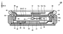
図2は、電子時計100の平面図である。
電子時計100は、金属等の導電性材料で形成された円筒状のケース胴80を備える。
ケース胴80の上側(表面側)には、セラミックやプラスチック等の非導電性材料で形成
された円筒状のガラス縁81が嵌合されており、ガラス縁81の開口は、透明なカバーガ
ラス84で塞がれている。また、ケース胴80のうち図中上側及び下側の2箇所には、ケ
ース胴80と一体的に形成された導電性のバンド取付部80aが設けられている。このバ
ンド取付部80aには、電子時計100を腕に装着するためのバンドが取り付けられる。
FIG. 2 is a plan view of the
The
A
ガラス縁81の内側には、プラスチックやセラミック等の非導電性材料で形成された円
環状のダイヤルリング83が配置され、ダイヤルリング83の内側には、円板状のダイヤ
ル板11が配置されている。ダイヤルリング83には、バータイプのインデックスが30
度おきに設けられており、各インデックスはその一部がダイヤル板11上に突出している
。また、ダイヤルリング83において隣り合うインデックス間には6度おきに目盛が刻ま
れている。なお、これらのインデックスや目盛をダイヤル板11に設けてもよいし、イン
デックスの代わりに“1”〜“12”までの数字を設けてもよい。このようにダイヤルリ
ング83やダイヤル板11は、図示の態様に限定されない。
An
Each index is provided at intervals, and a part of each index protrudes on the
ダイヤル板11の上には、指針軸12を中心に周回して現在時刻を指し示す指針13(
秒針13a、分針13b及び時針13c)が設けられている。ユーザーは、カバーガラス
84を介して、ダイヤルリング83、ダイヤル板11及び指針13を視認することができ
る。また、ダイヤルリング83の下側(裏面側)には、円環状のアンテナ体40が設けら
れている。
On the
また、電子時計100は、竜頭16や操作ボタン17,18を備える。竜頭16は3時
の位置に、操作ボタン17は2時の位置に、操作ボタン18は4時の位置に配置されてい
る。ユーザーは、竜頭16や操作ボタン17,18を操作することで、電子時計100の
動作モードを時刻情報取得モードや位置情報取得モードに設定することができる。時刻情
報取得モードは、少なくとも1基のGPS衛星20から衛星信号を受信してGPS時刻情
報や時刻補正パラメータを取得し、内部時刻を正確な時刻に修正する動作モードである。
また、位置情報取得モードは、少なくとも3基以上のGPS衛星20から衛星信号を受信
して電子時計100の位置情報を取得し、時差を反映させつつ内部時刻を正確な時刻に修
正する動作モードである。なお、電子時計100は、時刻情報取得モードや位置情報取得
モードを定期的に自動実行することも可能である。
The
The position information acquisition mode is an operation mode in which satellite signals are received from at least three
次に、電子時計100の内部構造について説明する。
図3は電子時計100の要部断面図であり、図4は電子時計100の要部分解斜視図で
ある。図3に示すように、円筒状のケース胴80の上側(表面側)には円筒状のガラス縁
81が嵌合されており、ガラス縁81の上側の開口は、円板状のカバーガラス84で塞が
れている。また、ケース胴80の下側(裏面側)の開口は、ステンレスやチタン等の導電
性材料で形成された裏蓋85で塞がれている。ケース胴80と裏蓋85は、例えばスクリ
ュー溝で固定されている。このように電子時計100の外装ケースは、例えば、ケース胴
80と、ガラス縁81と、カバーガラス84と、裏蓋85とで構成されている。
Next, the internal structure of the
3 is a cross-sectional view of the main part of the
カバーガラス84の下側には、ガラス縁81の内周に沿って円環状のダイヤルリング8
3が設けられている。ダイヤルリング83は、外周側がガラス縁81の内周面に接触する
平坦部分となっており、内周側は内側に向って傾斜する傾斜部分となっている。ダイヤル
リング83の下側にはドーナツ状の収納空間が設けられており、この収納空間に円環状の
アンテナ体40が収納されている。アンテナ体40は、ケース胴80やガラス縁81の内
周より内側に配置され、その上方がダイヤルリング83で覆われている。
An annular dial ring 8 is formed below the
3 is provided. The
アンテナ体40の下側には、金属等の導電性材料で形成された円環状のグランド板90
が設けられている。グランド板90には、図4に示すように、給電ピン44用の挿通孔9
0bの他に4個の孔が設けられており、4個の孔の各々には図3に示す導通ピン93が取
り付けられている。なお、導通ピン93を取り付けるための4個の孔は、グランド板90
の他に地板38や回路基板25の周縁部にも設けられている(図4参照)。各導通ピン9
3には、GPS受信部26や制御部70を含む回路ブロックのグランド電位が回路基板2
5を介して供給されており、グランド板90には計4個の導通ピン93のそれぞれからグ
ランド電位が供給されている。また、グランド板90には、図4に示すように4個の導通
ばね90aが形成されている。各導通ばね90aは、付勢力によってその一部がケース胴
80の内周面と接触しており(図3参照)、ケース胴80と電気的に接続されている。従
って、グランド電位は、グランド板90(各導通ばね90a)を介してケース胴80にも
供給されている。
An
Is provided. As shown in FIG. 4, the
In addition to 0b, four holes are provided, and a
In addition, it is also provided on the peripheral portion of the
3, the ground potential of the circuit block including the
5, and the ground potential is supplied to the
アンテナ体40の内側には、ダイヤル板11及びソーラーパネル87が設けられている
。ダイヤル板11は、プラスチック等の光透過性の非導電性材料で形成されている。また
、ソーラーパネル87は、光エネルギーを電気エネルギー(電力)に変換する複数のソー
ラーセル(光発電素子)を直列接続した円形の平板である。ダイヤル板11及びソーラー
パネル87は重ねて配置され、その中央には指針軸12が貫通する孔が設けられている。
A
ソーラーパネル87の下側には、プラスチックやセラミック等の非導電性材料で形成さ
れた地板38が設けられている。指針軸12は、ダイヤル板11、ソーラーパネル87及
び地板38を貫通して表裏方向に延在している。指針軸12は、ダイヤル板11と垂直な
方向から電子時計100を見たとき(すなわち電子時計100を平面視したとき)、電子
時計100の中心になる。また、指針13(13a〜13c)は、図3に示すようにアン
テナ体40の内周より内側で、カバーガラス84とダイヤル板11との間に配置されてい
る。
Under the
地板38の下側には、図3に示すように、指針軸12を回転させて指針13を駆動する
駆動機構30が設けられている。駆動機構30は、ステップモーターMと、歯車等の輪列
とを有し、ステップモーターMが輪列を介して指針軸12を回転させることにより指針1
3を駆動する。例えば、時針13cは12時間で1周し、分針13bは60分で一周し、
秒針13aは60秒で一周する。時刻表示部は、例えば、ダイヤル板11と、指針軸12
と、指針13(13a〜13c)と、駆動機構30とで構成されている。
As shown in FIG. 3, a
3 is driven. For example, the
The
And the pointer 13 (13a to 13c) and the
地板38及び駆動機構30の下側には、回路基板25が設けられている。この回路基板
25の下面(裏面側の面)には、GPS受信部26や制御部70を含む回路ブロックが実
装されている。GPS受信部26は、例えば1チップのICモジュールで構成され、アナ
ログ回路やデジタル回路が含まれる。制御部70は、GPS受信部26や駆動機構30の
動作を制御する。また、回路基板25の下面には二次電池27が配置されている(図3参
照)。二次電池27は、例えばリチウムイオン電池であり、ソーラーパネル87が発電し
た電力で充電される。
A
GPS受信部26や制御部70は、図3に示すように金属等の導電性材料で形成された
シールド板91で覆われている。シールド板91にはグランド電位が供給されており、グ
ランド電位は、シールド板91及び金属製の回路押え39を介して裏蓋85やケース胴8
0にも供給されている。なお、上述したようにグランド電位は、回路基板25及び各導通
ピン93を介してグランド板90やケース胴80にも供給されている。グランド電位の供
給経路を構成する各部材(例えば、シールド板91、回路押え39、裏蓋85、導通ピン
93、グランド板90、導通ばね90a等)は、部材間の接触面に金メッキや防錆用のメ
ッキ処理が施されている。また、各導通ピン93はネジ締め固定されている。これにより
グランド電位の供給経路を構成する各部材間での接触抵抗を長期間に亘ってできるだけ低
く抑えられるようにしている。
The
0 is also supplied. As described above, the ground potential is also supplied to the
また、回路基板25には、グランド電位を供給するための配線パターンや、アンテナ体
40に給電する所定の電位を供給するための配線パターンが形成されている。給電ピン4
4は、金属等の導電性材料で形成されたピン状のコネクタであり、コイルスプリングを内
蔵している。給電ピン44は、図4に示すように、地板38及びグランド板90に設けら
れた挿通孔38a,90bを介して回路基板25の上面とアンテナ体40の下面とを電気
的に接続している。給電ピン44の上端部は、コイルスプリングの付勢力によって、アン
テナ体40の下面(より具体的には、後述する給電部404)に接触している。また、給
電ピン44の下端部は、コイルスプリングの付勢力によって、回路基板25の上面(より
具体的には、所定の電位を供給する配線パターンが形成された部分)に接触している。こ
の給電ピン44を介してアンテナ体40に所定の電位が給電される。
In addition, a wiring pattern for supplying a ground potential and a wiring pattern for supplying a predetermined potential for supplying power to the
Reference numeral 4 denotes a pin-shaped connector formed of a conductive material such as metal, and incorporates a coil spring. As shown in FIG. 4, the
図5は、アンテナ体40の構造を説明するための図である。
図5(A)はアンテナ体40の斜視図であり、図5(B)はアンテナ体40の平面図で
ある。また、図5(C)は、アンテナ体40を図5(B)に示すG−g線で切断した断面
図である。
FIG. 5 is a view for explaining the structure of the
FIG. 5A is a perspective view of the
アンテナ体40は、プラスチックやセラミック等の誘電体で形成された円環状の基材4
01と、基材401の表面に形成された無給電素子402、給電素子403及び給電部4
04とを備える。無給電素子402、給電素子403及び給電部404は、いずれも金属
等の導電性材料で形成されており、例えばメッキや銀ペースト印刷等によって形成するこ
とができる。また、基材401の材料は、酸化チタン等の高周波で使用可能な誘電材料を
樹脂に混ぜることで、比誘電率が5〜20程度となるように調整されている。
The
01, a
04. The
図5(C)に示すように、基材401は、上面T1、外周面T2、底面T3、傾斜面T
P1及び傾斜面TP2によって囲まれた五角形の断面形状を有する。無給電素子402は
上面T1に形成されており、給電素子403は傾斜面TP1に形成されている。また、給
電部404は、傾斜面TP1、傾斜面TP2及び底面T3に亘って形成されている。給電
部404のうち、傾斜面TP1側の端部は給電素子403に接続され、底面T3側の端部
部分には給電ピン44の上端部が接触している。従って、給電素子403には、給電ピン
44及び給電部404を介して所定の電位が供給される。一方、無給電素子402に対し
ては外部から何ら電位は給電されない。
As shown in FIG. 5C, the
It has a pentagonal cross-sectional shape surrounded by P1 and the inclined surface TP2. The
また、図5(A)及び図5(B)に示すように、無給電素子402は、円環形状、すな
わち無端のO型形状に形成されている。一方、給電素子403は、切欠部405を有し、
円環の一部を切り欠いたC型形状に形成されている。給電素子403は、GPS衛星20
からの電波(衛星信号)に共振するアンテナ長を有する。例えば、給電部404と切欠部
405とのなす角をΦaとし、切欠部405の長さをΔsとし、給電素子403の円周長
をLとし、受信する円偏波の自由空間波長をλとしたとき、L=1.31λ、Φa=40
°、Δs=0.018λとすることができる。
Further, as shown in FIGS. 5A and 5B, the
It is formed in a C shape with a part of the ring cut out. The
It has an antenna length that resonates with radio waves (satellite signals). For example, the angle formed by the
°, Δs = 0.018λ.
また、C型形状を有する給電素子403の端部には給電部404が接続されている。図
5(B)に示すように、給電素子403のうち給電部404と接続された部分(端部)が
、所定の電位が給電される給電位置403aになる。給電位置403aは、例えば、電子
時計100において9時の方向に設けられている。つまり、電子時計100を平面視した
とき、電子時計100の中心(指針軸12)から見て9時の方向に、給電位置403a、
給電部404及び給電ピン44が設けられている。
In addition, a
A
図5(A)及び図5(B)に示すように、無給電素子402と給電素子403は一定の
離間間隔を保って並設されており、給電素子403に電流が流れると無給電素子402に
も電流が誘起される。つまり、無給電素子402と給電素子403の離間間隔は、両者の
間で電磁的な結合が可能になる距離に定められている。従って、給電素子403と無給電
素子402は、電磁的に結合し、両者が一体となって電磁波を電流に変換するアンテナ素
子として機能する。また、無給電素子402がO型形状を有することから、アンテナ体4
0は、全体としてO型形状のループアンテナとして機能する。電子時計100では、所定
の電位が給電される給電素子403と、グランド電位が供給されるグランド板90との間
で共振を生じさせ、この共振によってGPS衛星20からの電波(衛星信号)を受信する
。
As shown in FIGS. 5A and 5B, the
0 functions as an O-shaped loop antenna as a whole. In the
GPS衛星20からの衛星信号は1.575GHzであるので、1波長は約19cmに
なる。また、円偏波を受信するためには、波長の1.0〜1.2倍程度のアンテナ長が必
要になるので、衛星信号を受信するためには約19〜24cmのループアンテナが必要に
なる。このようなアンテナ長のループアンテナを腕時計の内部に収めようとすると、腕時
計の大型化を招いてしまう。
Since the satellite signal from the
例えば、比誘電率をεrとしたとき、比誘電率がεrの基材401を用いると、この基
材401による波長短縮率は1/√εrになる。つまり、比誘電率がεrの誘電体を用い
ることで、アンテナ体40の受信対象となる電波の波長を1/√εr倍に短縮することが
できる。上述したように基材401の比誘電率εrは5〜20程度であるので、基材40
1を備えない場合に比べ、アンテナ体40のアンテナ長を約0.224(εr=20)〜
0.447(εr=5)倍に短縮することができる。
For example, when the relative dielectric constant is εr and the
As compared with the case where 1 is not provided, the antenna length of the
It can be reduced to 0.447 (εr = 5) times.
また、無給電素子402を給電素子403に電磁的に結合させることでアンテナ体40
の共振周波数を下げてインピーダンス特性を改善することができる。このためアンテナ体
40の共振周波数を衛星信号に合わせることで、共振周波数でのリターンロスを減らし、
衛星信号に対するアンテナ体40の受信性能を高めることもできる。
Further, the
The impedance frequency can be improved by lowering the resonance frequency. Therefore, by matching the resonance frequency of the
It is also possible to improve the reception performance of the
なお、給電ピン44と給電部404との接触面や、給電ピン44と回路基板25との接
触面についても、金メッキや防錆用のメッキ処理を施すことで、接触抵抗を長期間に亘っ
てできるだけ低く抑えられるようにし、アンテナ体40の受信性能が低下しないようにし
ている。
The contact surface between the
図6は、アンテナ体40のXY平面における放射パターンを示すグラフである。
なお、図2〜図5の記載からも明らかとなるように、X軸方向とは、電子時計100を
平面視したとき、その中心(指針軸12)から3時に向う方向である。また、Y軸方向と
は、電子時計100を平面視したとき、その中心から12時に向う方向である。上述した
ように給電位置403aは、電子時計100を平面視したとき、その中心から見て9時の
方向に設けられている。これに対し、図6に示すようにアンテナ体40のXY平面におけ
る最大放射方向もこれとおおむね一致する。すなわち、同図に示すようにアンテナ体40
のXY平面における最大放射方向は、8時と9時の間の方向及びその反対方向になる。
FIG. 6 is a graph showing a radiation pattern on the XY plane of the
2 to 5, the X-axis direction is a direction from the center (pointer shaft 12) to 3 o'clock when the
The maximum radiation direction in the XY plane is between 8 o'clock and 9 o'clock and vice versa.
電子時計100では装着者が屋外にいるときに衛星信号を受信することになるが、屋外
の場合、装着者は、図7に示すように電子時計100を装着した腕を下げているかその手
を身体の前に位置させた姿勢でいることが多い。このような姿勢の場合、図7に示すよう
に、電子時計100ではその中心から9時に向かう方向が天頂方向になる。従って、給電
位置403a(給電部404や給電ピン44の設置位置)を電子時計100の中心から見
て9時の方向の付近に設けることで、装着者が屋外にいるときにアンテナ体40の最大放
射方向が天頂方向に向けられている確率を高めることができる。
The
ところで、給電ピン44や給電部404は、給電素子403と電気的に接続されており
、給電素子403と同電位であるので、ループアンテナの一部とみなされる。
By the way, the
また、図2に示したように、電子時計100のうち2時から4時までの部分には、竜頭
16や操作ボタン17,18が設けられている。竜頭16や操作ボタン17,18は、い
ずれも金属等の導電性材料で形成されている。また、竜頭16からは、金属等の導電性材
料で形成された巻真(図示省略)がケース胴80を貫通して電子時計100の中心方向に
向って延在している。同様に操作ボタン17,18からも、金属等の導電性材料で形成さ
れたボタン軸(図示省略)がケース胴80を貫通して電子時計100の中心方向に向って
延在している。これらの竜頭16、操作ボタン17,18、巻真及びボタン軸(以下、操
作部材)の近くに給電ピン44や給電部404を設けると、いずれも導電性材料で形成さ
れていることから、共振が生じたり、アンテナ体40の近傍における電流密度が変化し、
アンテナ体40の受信性能が低下してしまう。
Further, as shown in FIG. 2, the
The reception performance of the
従って、アンテナ体40の良好な受信性能を維持するためには、操作部材の近くに給電
ピン44や給電部404を配置しないようにする必要がある。実験を行って確認したとこ
ろ、図2に示したように竜頭16や操作ボタン17,18が2時から4時までの部分に設
けられている場合、給電ピン44や給電部404を5時から1時まで(5時→9時→1時
)の範囲に設ければ、アンテナ体40の受信性能を十分に維持できることがわかった。つ
まり、操作部材を考慮すると、アンテナ体40の良好な受信性能を維持するためには、給
電位置403a(給電部404や給電ピン44の設置位置)を電子時計100の中心から
見て5時の方向から1時の方向までの範囲に設ける必要がある。
Therefore, in order to maintain a good reception performance of the
また、アンテナ体40はグランド板90との共振により衛星信号を受信するが、アンテ
ナ体40の近傍には、グランド板90の他にも導電性の部材としてケース胴80が存在し
、このケース胴80も共振の対象に含まれる。図2に示したように、ケース胴80には、
11時から1時までの部分と5時から7時までの部分に導電性材料で形成されたバンド取
付部80aが設けられており、この部分は他の部分に比べ、外形が大きく突起して体積が
大幅に増えている。このためバンド取付部80aの近くに給電ピン44や給電部404を
設けると、バンド取付部80aによる損失でアンテナ体40の受信性能が低下してしまう
。
The
A
従って、アンテナ体40の良好な受信性能を維持するためには、バンド取付部80aの
近くに給電ピン44や給電部404を配置しないようにする必要がある。実験を行って確
認したところ、図2に示したようにバンド取付部80aが11時から1時までの部分と5
時から7時までの部分に設けられている場合、給電ピン44や給電部404を2時から4
時までの範囲又は8時から10時までの範囲に設ければ、アンテナ体40の受信性能を十
分に維持できることがわかった。つまり、バンド取付部80aを考慮すると、アンテナ体
40の良好な受信性能を維持するためには、給電位置403a(給電部404や給電ピン
44の設置位置)を電子時計100の中心から見て2時の方向から4時の方向までの範囲
又は8時の方向から10時の方向までの範囲に設ける必要がある。
Therefore, in order to maintain the good reception performance of the
When it is provided in the part from time to 7 o'clock, the
It was found that the reception performance of the
以上のようなことから、操作部材とバンド取付部80aの両方を考慮してアンテナ体4
0の良好な受信性能を維持しつつ、装着者が屋外にいるときにアンテナ体40の最大放射
方向が天頂方向に向けられている確率を高めるためには、図8に示すように、給電位置4
03aを電子時計100の中心(指針軸12)から見て8時の方向から10時の方向まで
の範囲に設ければよいことになる。従って、給電ピン44や給電部404の設置位置は、
電子時計100の中心から見て9時の方向に限定されず、8時の方向から10時の方向ま
での範囲に設けられていればよい。
From the above, the antenna body 4 in consideration of both the operation member and the
In order to increase the probability that the maximum radiation direction of the
It is sufficient to provide 03a in the range from the 8 o'clock direction to the 10 o'clock direction when viewed from the center of the electronic timepiece 100 (pointer shaft 12). Therefore, the installation positions of the power supply pins 44 and the
It is not limited to the 9 o'clock direction when viewed from the center of the
図9は、電子時計100の回路構成を示すブロック図である。
電子時計100は、例えば、GPS受信部26と制御表示部36とを含んで構成されて
いる。GPS受信部26は、衛星信号の受信、GPS衛星20の捕捉、位置情報の生成、
時刻修正情報の生成等に関する処理を行う。また、制御表示部36は、内部時刻の計時や
修正、指針13の運針等に関する処理を行う。
FIG. 9 is a block diagram showing a circuit configuration of the
The
Processing related to generation of time correction information is performed. In addition, the
ソーラーパネル87は、充電制御回路29を介して二次電池27を充電する。二次電池
27は、レギュレーター34を介して制御表示部36に駆動電力を供給すると共に、レギ
ュレーター35を介してGPS受信部26に駆動電力を供給する。電圧検出回路37は、
二次電池27の電圧を検出して制御部70に出力する。なお、レギュレーター35を、R
F(Radio Frequency)部50に駆動電力を供給するレギュレーターと、ベースバンド部
60に駆動電力を供給するレギュレーターとに分けてもよい。この場合、RF部50に駆
動電力を供給するレギュレーターは、RF部50の内部に設けてもよい。
The
The voltage of the
The regulator may be divided into a regulator that supplies driving power to an F (Radio Frequency)
定電位発生回路33は、グランド電位に対して予め定められた電位差を有する所定の電
位を生成する。定電位発生回路33で生成された所定の電位は、回路基板25及び給電ピ
ン44を介してアンテナ体40(給電素子403)に給電される。
The constant
アンテナ体40は、GPS衛星20からの衛星信号を受信する。但し、アンテナ体40
は衛星信号以外の不要な電波も若干受信してしまうため、アンテナ体40の後段にはSA
W(Surface Acoustic Wave)フィルター32が設けられている。SAWフィルター32
は、1.5GHz帯の信号を通過させるバンドパスフィルターとして機能し、アンテナ体
40が受信した信号から衛星信号を抽出する。
The
Receives a small amount of unnecessary radio waves other than satellite signals.
A W (Surface Acoustic Wave) filter 32 is provided.
Functions as a bandpass filter that allows 1.5 GHz band signals to pass through, and extracts satellite signals from signals received by the
GPS受信部26は、例えば、RF部50とベースバンド部60とを含んで構成されて
いる。また、RF部50は、例えば、LNA(Low Noise Amplifier)51、ミキサー5
2、VCO(Voltage Controlled Oscillator)53、PLL(Phase Locked Loop)回路
54、IF(Intermediate Frequency)アンプ55、IFフィルター56、ADC(A/
D変換器)57等を含んで構成されている。
The
2, VCO (Voltage Controlled Oscillator) 53, PLL (Phase Locked Loop)
D converter) 57 and the like.
SAWフィルター32を通過した信号(衛星信号)は、RF部50に入力されてLNA
51で増幅される。LNA51で増幅された衛星信号は、VCO53が出力するクロック
信号とミキサー52でミキシングされ、中間周波数帯の信号にダウンコンバートされる。
PLL回路54は、VCO53の出力クロック信号を分周したクロック信号と、ベースバ
ンド部60から供給される基準クロック信号とを位相比較してVCO53の出力クロック
信号を基準クロック信号に同期させる。従って、VCO53は、周波数精度が高い安定し
たクロック信号を出力することができる。なお、中間周波数として、例えば数MHzを選
択することができる。
The signal (satellite signal) that has passed through the
51 is amplified. The satellite signal amplified by the
The
ミキサー52から出力された中間周波数帯の信号は、IFアンプ55で増幅される。但
し、ミキサー52でのミキシングによって数GHzの高周波成分が発生してしまうため、
IFアンプ55では中間周波数帯の信号と共に数GHzの高周波成分も増幅してしまうこ
とになる。このためIFフィルター56では、中間周波数帯の信号を抽出すると共に、高
周波成分を除去する(正確には、所定のレベル以下に減衰させる)。IFフィルター56
を通過した中間周波数帯の信号は、ADC57でデジタル信号に変換される。
The intermediate frequency band signal output from the
The
The signal in the intermediate frequency band that has passed through is converted into a digital signal by the
ベースバンド部60は、例えば、DSP(Digital Signal Processor)61、CPU(
Central Processing Unit)62、SRAM(Static Random Access Memory)63、RT
C(Real Time Clock)64等を含んで構成されている。また、ベースバンド部60には
、TCXO(Temperature Compensated Crystal Oscillator:温度補償回路付き水晶発振
回路)65や、フラッシュメモリー66が接続されている。
The
Central Processing Unit (62), SRAM (Static Random Access Memory) 63, RT
C (Real Time Clock) 64 and the like. In addition, a TCXO (Temperature Compensated Crystal Oscillator) 65 and a
TCXO65は、温度に関係なくほぼ一定の周波数の基準クロック信号を生成する。ベ
ースバンド部60の動作は、TCXO65が出力する基準クロック信号に同期する。RT
C64は、衛星信号を処理するためのタイミングを生成するものであり、TCXO65か
ら出力される基準クロック信号でカウントアップされる。フラッシュメモリー66には、
例えば時差情報が記憶されている。時差情報は、UTCに対する時差を座標値(例えば緯
度及び経度)と関連付けて定義した情報である。
The
C64 generates timing for processing the satellite signal, and is counted up by the reference clock signal output from the
For example, time difference information is stored. The time difference information is information that defines a time difference with respect to UTC in association with coordinate values (for example, latitude and longitude).
ベースバンド部60は、時刻情報取得モードや位置情報取得モードが設定されている場
合に、RF部50のADC57から出力されるデジタル信号(中間周波数帯の信号)から
ベースバンド信号を復調する処理を行う。
The
また、ベースバンド部60は、時刻情報取得モードや位置情報取得モードが設定されて
いる場合に、衛星検索工程において、各C/Aコードと同一のパターンのローカルコード
を発生し、ベースバンド信号に含まれているC/Aコードとの相関をとる処理を行う。ベ
ースバンド部60は、各ローカルコードに対する相関値がピークになるようにローカルコ
ードの発生タイミングを調整し、相関値が閾値以上となる場合にはそのローカルコードの
GPS衛星20に同期(すなわちGPS衛星20を捕捉)したものと判断する。GPSで
は、全てのGPS衛星20が異なるC/Aコードを用いて同一周波数で衛星信号を送信す
るCDMA(Code Division Multiple Access)方式を採用している。従って、ベースバ
ンド信号に含まれているC/Aコードを判別することで、捕捉可能なGPS衛星20を検
索することができる。
In addition, when the time information acquisition mode and the position information acquisition mode are set, the
また、ベースバンド部60は、捕捉したGPS衛星20の衛星信号から航法メッセージ
を取得する場合、捕捉したGPS衛星20のC/Aコードと同一のパターンのローカルコ
ードと、ベースバンド信号とをミキシングする処理を行う。これにより捕捉したGPS衛
星20の航法メッセージが復調される。ベースバンド部60は、航法メッセージの各サブ
フレームのTLMワード(プリアンブルデータ)を検出し、サブフレームに含まれている
GPS時刻情報や軌道情報等の衛星情報を取得してSRAM63に記憶する。なお、GP
S時刻情報は、週番号データ(WN)及びZカウントデータであるが、週番号データが取
得済みの場合はZカウントデータのみを取得すればよい。
Further, when acquiring a navigation message from the satellite signal of the captured
The S time information is week number data (WN) and Z count data. If the week number data has already been acquired, only the Z count data need be acquired.
また、ベースバンド部60は、衛星情報に基づいて時刻修正情報を生成する。時刻修正
情報は、電子時計100で計時されている内部時刻を修正するための情報である。ベース
バンド部60は、時刻情報取得モードの場合、例えば、1基のGPS衛星20の衛星情報
に含まれているGPS時刻情報,時刻補正パラメータ,UTCオフセット等を使用して時
刻修正情報を生成することができる。なお、ベースバンド部60は、複数のGPS衛星2
0の衛星情報から時刻修正情報を生成してもよい。時刻情報取得モードの場合の時刻修正
情報は、例えば、GPS時刻情報そのものであってもよいし、時刻補正パラメータで補正
した後のGPS時刻情報であってもよいし、GPS時刻情報に対して時刻補正パラメータ
やUTCオフセットを加算して得られる時刻情報であってもよい。また、これらの時刻情
報と内部時刻情報との時間差を示す情報を時刻修正情報としてもよい。
In addition, the
Time correction information may be generated from zero satellite information. The time correction information in the time information acquisition mode may be, for example, GPS time information itself, GPS time information after correction with a time correction parameter, or time relative to GPS time information. Time information obtained by adding a correction parameter or UTC offset may be used. Information indicating the time difference between the time information and the internal time information may be time correction information.
また、ベースバンド部60は、位置情報取得モードの場合、最低3基(通常は4基)以
上のGPS衛星20から衛星情報を受信し、まず、受信した衛星情報を使用して電子時計
100の位置情報を取得する。次に、ベースバンド部60は、フラッシュメモリー66に
記憶されている時差情報を参照し、取得した位置情報に対応する時差データを取得する。
この後、ベースバンド部60は、時刻情報取得モードの場合と同様の方法で生成した時刻
修正情報に対し、取得した時差データを加算して位置情報取得モードの場合の時刻修正情
報とする。このように位置情報取得モードの場合の時刻修正情報は、電子時計100の現
在位置に応じた時差を反映させたものとなる。
Further, in the position information acquisition mode, the
Thereafter, the
制御表示部36は、例えば、制御部70、水晶振動子73、駆動回路74等を含んで構
成されている。また、制御部70は、例えば、記憶部71やRTC72等を備えたCPU
で構成することができる。制御部70は、GPS受信部26に対して制御信号を出力し、
GPS受信部26の動作を制御する。また、制御部70は、駆動回路74を介して指針1
3(13a〜13c)の運針等を制御する。また、制御部70は、電圧検出回路37の検
出結果等に基づいてレギュレーター34,35や定電位発生回路33の動作を制御する。
The
Can be configured. The
The operation of the
3 (13a to 13c) is controlled. The
記憶部71には、GPS受信部26から出力された時刻修正情報や位置情報等が記憶さ
れる。RTC72は内部時刻を計時している。RTC72は、常時駆動されており、水晶
振動子73によって生成される基準クロック信号でカウントアップされる。従って、制御
部70は、時刻情報取得モードや位置情報取得モードでない場合であっても、RTC72
で計時されている内部時刻に基づいて指針13の運針を継続することができる。
The
The hand movement of the
また、制御部70は、時刻情報取得モードや位置情報取得モードの場合にGPS受信部
26から時刻修正情報が出力されると、RTC72で計時されている内部時刻を時刻修正
情報に従って修正する。また、内部時刻を修正した場合、制御部70は、修正後の内部時
刻を指針13(13a〜13c)が指し示すように駆動回路74を介して指針13を駆動
する。これにより電子時計100の内部時刻が正確な時刻に修正される。特に位置情報取
得モードの場合は、電子時計100の現在位置に応じた時差を反映させつつ内部時刻を正
確な時刻に修正することができる。
In addition, when the time correction information is output from the
以上説明したように本実施形態によれば、アンテナ体40を構成する円環状の基材40
1(誘電体)には、C型形状を有すると共に所定の電位が給電される給電素子403と、
O型形状の無給電素子402とが一定の離間間隔を保って並設されている。この場合、給
電素子403に電流が流れると無給電素子402にも電流が誘起されるので、給電素子4
03と無給電素子402とが電磁的に結合し、両者が一体となって電磁波を電流に変換す
るアンテナ素子として機能する。また、アンテナ体40は、全体としてO型形状のループ
アンテナとして機能する。このようなループアンテナでは、ループ面を含む平面(XY平
面)における放射指向性が円環の中心から見て給電位置403a(給電ピン44や給電部
404の設置位置)が設けられた方向又はその付近で最大になる。
As described above, according to the present embodiment, the
1 (dielectric) has a C-shape and a
An O-shaped
03 and the
従って、電子時計100を平面視したとき、その中心(指針軸12)から見て8時の方
向から10時の方向までの範囲に給電位置403aを設けることで、図7に示したように
、装着者が電子時計100を装着した腕を下げているかその手を身体の前に位置させた姿
勢でいるときに、アンテナ体40の最大放射方向を天頂方向に向けることができるから、
アンテナ体40の受信性能を十分に発揮させることが可能になる。このように本実施形態
によれば、装着者が屋外で多くとる姿勢に基づいて実用上最適なアンテナ指向性を得るこ
とができる。
また、本実施形態によれば、アンテナ体40は円環状の基材401(誘電体)を備える
ので、誘電体の波長短縮効果と相俟ってアンテナ体40の周囲長を短縮することができ、
これによりアンテナ体40を小型化することができる。
また、本実施形態によれば、無給電素子402を給電素子403に電磁的に結合させる
ことでアンテナ体40の共振周波数を下げてインピーダンス特性を改善することができる
。このためアンテナ体40の共振周波数を衛星信号に合わせることで、共振周波数でのリ
ターンロスを減らし、衛星信号に対するアンテナ体40の受信性能を高めることもできる
。
よって、本実施形態によれば、十分な受信性能を維持しつつアンテナ体40を小型化す
ることができる。
Accordingly, when the
The reception performance of the
In addition, according to the present embodiment, the
Thereby, the
In addition, according to the present embodiment, the
Therefore, according to this embodiment, the
また、本実施形態によれば、アンテナ体40の基材401をその円環の中心軸方向から
見たとき(図5(B)参照)、給電素子403は無給電素子402の内側に設けられてい
る。アンテナ体40の近傍は電流密度が高く外部からの影響に敏感な部分であるため、外
装ケースの側面を構成するケース胴80を金属等の導電性材料で形成した場合、ケース胴
80を指で触るとアンテナ体40の受信特性が不安定になる。給電素子403を無給電素
子402の内側に設けることで、給電素子403を無給電素子402の外側に設けた場合
に比べ、ケース胴80から給電素子403までの距離を長くとることができるから、アン
テナ体40の受信特性を安定させることができる。
Further, according to the present embodiment, when the
また、本実施形態によれば、アンテナ体40を構成する円環状の基材401は、外周側
に位置する平坦な上面T1と、内周側に位置し、内側に向かうほどダイヤル板11に対す
る高さが小さくなる傾斜面TP1とを有し、給電素子403は傾斜面TP1に設けられて
いる。この場合も、ケース胴80から給電素子403までの距離を長くとることができる
から、アンテナ体40の受信特性を安定させることができる。また、傾斜面TP1は内側
に向かうほどダイヤル板11に対する高さが小さくなるから、ダイヤル板11を広い角度
方向から視認することが可能になる。また、このような傾斜面TP1に給電素子403を
設けることで、受信することができる電波の角度方向が広がるので、アンテナ体40の良
好な受信性能を確保することが可能になる。また、傾斜面TP1を設けることで電子時計
100が薄く見え、見栄えが向上する。
Further, according to the present embodiment, the
本発明は、上述した実施形態に限定されるものではなく、例えば以下に述べる変形が可
能である。また、以下に示す2以上の変形を適宜組み合わせることもできる。
The present invention is not limited to the above-described embodiment, and for example, the following modifications are possible. Also, two or more of the following modifications can be combined as appropriate.
[変形例1]
図5に示したアンテナ体40において、無給電素子402は、無端のO型形状に限らず
、給電素子403と同様に切欠部を有するC型形状に形成されてもよい。この場合、アン
テナ体40は全体としてC型形状のループアンテナとして機能する。また、図5に示した
アンテナ体40において、給電位置403aは、給電素子403の端部に設けられる態様
に限らず、給電素子403のうち端部以外の部分に設けられてもよい。また、上述した実
施形態では、給電素子403の長さを衛星信号に共振するように定める場合を例示したが
、無給電素子402の長さを衛星信号に共振するように定めてもよい。この場合、給電素
子403の長さや切欠部405の位置等を調整することで、アンテナ体40と、アンテナ
体40に電気的に接続される回路(GPS受信部26や制御部70を含む回路ブロック)
との間のインピーダンスを容易に整合させることができる。
[Modification 1]
In the
The impedance between the two can be easily matched.
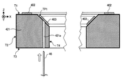
[変形例2]
図10は、変形例2に係るアンテナ体の断面図であり、図5(C)と同様に見た図であ
る。本変形例に係るアンテナ体の基材411は、傾斜面TP2を有しておらず、傾斜面T
P1が底面T3に連なっている。また、基材411の上面T1は、図5(C)の場合に比
べて小さく形成されており、大きな傾斜面TP1が設けられる。傾斜面TP1には、給電
素子403に加えて無給電素子402が形成されており、上面T1には何ら部材が配置さ
れていない。このように給電素子403と無給電素子402の両方を傾斜面TP1に設け
てもよい。
[Modification 2]
FIG. 10 is a cross-sectional view of an antenna body according to Modification 2, and is a view seen in the same manner as FIG. The
P1 continues to the bottom surface T3. Moreover, the upper surface T1 of the
[変形例3]
図11は、変形例3に係るアンテナ体の断面図であり、図5(C)と同様に見た図であ
る。本変形例に係るアンテナ体の基材421は、傾斜面TP2の代わりに直立した内周面
T4を有する。また、無給電素子412及び給電素子413の全体と、給電部424の一
部とが基材421の内部に埋設されている。このような構造は、インサート成形で製造す
ることができる。インサート成形によれば、メッキや銀ペースト印刷等によって図5(C
)に示すように基材401の表面に無給電素子402、給電素子403及び給電部404
を形成する場合に比べ、アンテナ体を安価に製造することができる。
[Modification 3]
FIG. 11 is a cross-sectional view of an antenna body according to
), The
As compared with the case of forming the antenna body, the antenna body can be manufactured at a low cost.
[変形例4]
図12は、変形例4に係るアンテナ体の断面図であり、図5(C)と同様に見た図であ
る。同図に示すように、無給電素子402や給電素子403を、フレキシブルテープ50
0で基材401に貼り付けてもよい。例えば、あらかじめフレキシブルテープ500上に
無給電素子402や給電素子403を形成し、このフレキシブルテープ500を基材40
1の表面(上面T1及び傾斜面TP1)に貼り付けることで、このような構造を製造する
ことができる。この製造方法によれば、無給電素子402や給電素子403をメッキや銀
ペースト印刷等によって基材401の表面に直接形成する場合に比べ、アンテナ体を安価
に製造することができる。なお、給電部404についてもフレキシブルテープ500を用
いて基材401に貼り付けるようにしてもよい。
[Modification 4]
FIG. 12 is a cross-sectional view of an antenna body according to Modification 4, and is a view seen in the same manner as FIG. As shown in the figure, the
0 may be attached to the
Such a structure can be manufactured by affixing to 1 surface (upper surface T1 and inclined surface TP1). According to this manufacturing method, the antenna body can be manufactured at a lower cost than when the
[変形例5]
図13は、変形例5に係るアンテナ体の断面図であり、図5(C)と同様に見た図であ
る。本変形例に係るアンテナ体の基材431は、上面T11、外周面T12、底面T13
及び内周面T14によって囲まれた四角形の断面形状を有する。無給電素子402と給電
素子403は上面T11に形成されている。また、給電部434は、上面T11、内周面
T14及び底面T13に亘って形成されている。このようにアンテナ体の基材431は、
傾斜面TP1を有していなくてもよい。なお、無給電素子402と給電素子403の配置
を逆転させてもよい。つまり、給電素子403を無給電素子402の外側に設けてもよい
。この場合、給電部434は、上面T11、外周面T12及び底面T13に亘って形成さ
れる。また、このように給電部434を外周面T12に形成する場合、ケース胴80をセ
ラミックやプラスチック等の非導電性材料で形成することが望ましい。
[Modification 5]
FIG. 13 is a cross-sectional view of an antenna body according to
And a quadrangular cross-sectional shape surrounded by the inner peripheral surface T14. The
The inclined surface TP1 may not be provided. The arrangement of the
[変形例6]
給電ピン44は、給電素子403と電気的に接続されており、給電素子403と同電位
であるため、ループアンテナの一部とみなされる。また、給電ピン44に内蔵されている
コイルスプリングは、電流が流れることで磁界を発生させてしまうことに加え、電子時計
100内の各種回路やステップモーターM等から発生したノイズを拾ってしまうので、こ
れらの磁界やノイズの影響でアンテナ体40の受信性能が低下してしまう。そこで、給電
ピン44を以下のように変形してもよい。
[Modification 6]
Since the
図14は、変形例6に係る給電ピン45の要部断面図である。
本変形例に係る給電ピン45は、金属等の導電性材料で形成されたコイルスプリング4
51を内蔵している。コイルスプリング451の両端には、金属等の導電性材料で形成さ
れた端子452a,452bが接続されている。端子452aは、コイルスプリング45
1の付勢力によって基材401の底面T3に形成された給電部404と接触しており、給
電部404と電気的に接続されている。また、端子452bは、コイルスプリング451
の付勢力によって回路基板25の上面に形成された配線パターン25aと接触しており、
配線パターン25aと電気的に接続されている。配線パターン25aには、給電素子40
3に給電する所定の電位が供給されている。また、給電ピン45は、筒状のシールドケー
ス453を備える。このシールドケース453は、金属等の導電性材料で形成された外周
壁453aと、ガラスやプラスチック等の絶縁体で形成された内周壁453bとで構成さ
れており、外周壁453aにはグランド電位VGNDが供給されている。
FIG. 14 is a cross-sectional view of a main part of a
The
51 is built-in.
1 is in contact with the
Is in contact with the
The
3 is supplied with a predetermined potential for supplying power. The
以上の構成によれば、コイルスプリング451の側面部分はグランド電位VGNDが供
給される外周壁453aで囲まれているので、外周壁453aが磁気的なシールドとして
機能する。従って、コイルスプリング451が発生させた磁界でアンテナ体40の近傍に
おける電流密度が変化してしまうことや、電子時計100内の各種回路やステップモータ
ーM等から発生したノイズをコイルスプリング451が拾ってしまうことを抑制し、アン
テナ体40の良好な受信性能を維持することができる。なお、給電ピン45は端子452
a,452bを備えず、コイルスプリング451の一方の端部(図中上側)が基材401
の底面T3に形成された給電部404に直接接触し、コイルスプリング451の他方の端
部(図中下側)が回路基板25の上面に形成された配線パターン25aに直接接触する構
成であってもよい。
According to the above configuration, since the side surface portion of the
a, 452b are not provided, and one end portion (upper side in the figure) of the
The other end (lower side in the figure) of the
[変形例7]
給電ピン44の代わりに、板ばね、リード線、同軸ケーブル、フレキシブル基板等を使
用してアンテナ体40の給電部404と回路基板25とを電気的に接続し、所定の電位を
給電してもよい。
[Modification 7]
Even if a plate spring, a lead wire, a coaxial cable, a flexible substrate, or the like is used instead of the
[変形例8]
図15は、変形例8に係るアンテナ体の断面図であり、図5(C)と同様に見た図である。本変形例に係るアンテナ体が図5に示したアンテナ体40と異なるのは、(1)基材421が傾斜面TP2の代わりに直立した内周面T4を有している点、(2)給電部404が設けられていない点、(3)基材421の傾斜面TP1から底面T3にかけて挿入孔421aが設けられている点である。なお、挿入孔421aの数は1個であり、上述した実施形態で説明した給電位置403aと同様に、電子時計100を平面視したとき、その中心(指針軸12)から見て8時の方向から10時の方向までの範囲に設けられている。また、本変形例に係るアンテナ体を使用する場合は、上述した実施形態で説明した給電ピン44の代わりに棒状の給電ピン46を使用する。この給電ピン46は、金属等の導電性材料で形成されており、一方の端部が挿入孔421aに挿入されてその先端が給電素子403に接続される。また、他方の端部は、回路基板25上の配線パターンに接続されて所定の電位が供給される。同図に示す構成の場合、基材421(誘電体)の表面に給電部404を形成する必要がない。このようにアンテナ体には給電部404が設けられていなくてもよい。
[Modification 8]
FIG. 15 is a cross-sectional view of an antenna body according to Modification 8 and is a view seen in the same manner as FIG. The antenna body according to this modification differs from the
[変形例9]
秒針13aはなくてもよい。また、時刻表示部は、ダイヤル板11の上で指針13を周
回させて時刻を指し示す態様の他、例えば、ダイヤル板11に相当する大きさの表示領域
を有する液晶表示パネルを備え、ダイヤル板11や指針13の画像を表示領域に表示して
時刻を表示する態様であってもよい。
[Modification 9]
The
[変形例10]
図16は、変形例10に係る電子時計200の平面図である。
本変形例に係る電子時計200は、直方体状の外装ケースを備え、その内部に環状のア
ンテナ体41を収納している。アンテナ体41の環(輪)の形状は略四角形である。また
、アンテナ体41の内側には、時刻をデジタル表示する液晶表示パネル15が設けられて
いる。なお、アンテナ体41は、環の形状が異なるものの、図5に示したアンテナ体40
と同様に、例えば、基材(誘電体)、無給電素子、給電素子及び給電部を備え、給電素子
には、給電ピンや給電部を介して所定の電位が給電される。このようなデジタル表示方式
の電子時計200においても、電子時計200を平面視したとき、電子時計200の中心
点Cから見て8時の方向から10時の方向までの範囲(図中ハッチングで示す部分)に、
給電位置(給電ピンや給電部の設置位置)が設けられていればよい。
[Modification 10]
FIG. 16 is a plan view of an
An
Similarly, for example, a substrate (dielectric), a parasitic element, a feeding element, and a feeding section are provided, and a predetermined potential is fed to the feeding element via a feeding pin and a feeding section. Also in such a digital display type
It suffices if a power supply position (position of the power supply pin or power supply unit) is provided.
[変形例11]
導通ピン93や導通ばね90aの数は4個に限らず1以上であればよい。また、グラン
ド板90や導通ばね90aはなくてもよく、この場合、給電素子403の共振対象はケー
ス胴80になる。また、上述した実施形態では、外装ケースの側面をケース胴80とガラ
ス縁81で構成した場合を例示したが、外装ケースの側面は、セラミックやプラスチック
等の非導電性材料で形成された1つの部材で構成されてもよい。また、ソーラー充電以外
の充電方式を採用してもよい。例えば、充電コイルを備え、外部充電器から電磁誘導で電
力を充電できるようにしてもよい。また、二次電池27に代えてリチウム電池等の一次電
池を用いてもよい。
[Modification 11]
The number of
[変形例12]
GPSの代わりに、ガリレオ(EU)、GLONASS(ロシア)、北斗(中国)、I
RNSS(インド)等の全地球航法衛星システム(GNNS)を利用してもよいし、静止
衛星型衛星航法補強システム(SBAS)や準天頂衛星システム(QZSS)を利用して
もよい。このように電子時計100は、GPS衛星20以外の人工衛星からの電波を受信
して内部時刻の修正等を行ってもよい。
[Modification 12]
Instead of GPS, Galileo (EU), GLONASS (Russia), Hokuto (China), I
A global navigation satellite system (GNNS) such as RNSS (India) may be used, or a geostationary satellite type satellite navigation augmentation system (SBAS) or a quasi-zenith satellite system (QZSS) may be used. As described above, the
100,200…電子時計(アンテナ内蔵式電子時計)、11…ダイヤル板、12…指
針軸、13(13a,13b,13c)…指針、15…液晶表示パネル、25…回路基板
、26…GPS受信部、30…駆動機構、33…定電位発生回路、38…地板、40,4
1…アンテナ体、401,411,421,431…基材、421a…挿入孔、402,
412…無給電素子、403,413…給電素子、403a…給電位置、404,414
,424,434…給電部、405…切欠部、44,45,46…給電ピン、451…コ
イルスプリング、452a,452b…端子、453…シールドケース、453a…外周
壁、453b…内周壁、70…制御部、80…ケース胴、80a…バンド取付部、81…
ガラス縁、83…ダイヤルリング、84…カバーガラス、85…裏蓋、87…ソーラーパ
ネル、90…グランド板、91…シールド板、93…導通ピン、500…フレキシブルテ
ープ、T1,T11…上面、T2,T12…外周面、T3,T13…底面、T4,T14
…内周面、TP1,TP2…傾斜面、C…中心点。
DESCRIPTION OF SYMBOLS 100,200 ... Electronic timepiece (electronic timepiece with built-in antenna), 11 ... Dial plate, 12 ... Pointer shaft, 13 (13a, 13b, 13c) ... Pointer, 15 ... Liquid crystal display panel, 25 ... Circuit board, 26 ... GPS reception , 30... Drive mechanism, 33... Constant potential generation circuit, 38.
DESCRIPTION OF SYMBOLS 1 ... Antenna body, 401,411,421,431 ... Base material, 421a ... Insertion hole, 402,
412: Parasitic element, 403, 413 ... Power feeding element, 403a ... Power feeding position, 404, 414
, 424, 434 ... feed section, 405 ... notch section, 44,45,46 ... feed pin, 451 ... coil spring, 452a, 452b ... terminal, 453 ... shield case, 453a ... outer peripheral wall, 453b ... inner peripheral wall, 70 ... Control unit, 80 ... case body, 80a ... band attachment part, 81 ...
Glass edge, 83 ... Dial ring, 84 ... Cover glass, 85 ... Back cover, 87 ... Solar panel, 90 ... Ground plate, 91 ... Shield plate, 93 ... Conduction pin, 500 ... Flexible tape, T1, T11 ... Top surface, T2 , T12 ... outer peripheral surface, T3, T13 ... bottom surface, T4, T14
... inner peripheral surface, TP1, TP2 ... inclined surface, C ... center point.
Claims (4)
前記外装ケースに収納された環状のアンテナ体と、
前記外装ケースに収納され、時刻を表示する時刻表示部と、
を備えたアンテナ内蔵式電子時計において、
前記アンテナ体は、
環状の誘電体と、
前記誘電体上に設けられ、環状の一部を切り欠いた形状を有し、所定の電位が給電され
る導電性の給電素子と、
前記誘電体上に前記給電素子と離間して設けられ、環状又は環状の一部を切り欠いた形
状を有する導電性の無給電素子と、を備え、
前記給電素子には、前記所定の電位が給電される給電位置が一箇所設けられ、
前記給電位置は、当該アンテナ内蔵式電子時計を平面視したとき、当該アンテナ内蔵式
電子時計の中心から見て8時の方向から10時の方向までの範囲に設けられている
ことを特徴とするアンテナ内蔵式電子時計。 An exterior case,
An annular antenna body housed in the exterior case;
A time display unit that is stored in the outer case and displays the time;
In the electronic watch with a built-in antenna,
The antenna body is
An annular dielectric,
A conductive power supply element that is provided on the dielectric and has a shape in which a part of the ring is cut out;
A conductive parasitic element that is provided on the dielectric so as to be spaced apart from the feeding element and has a ring shape or a shape in which a part of the ring shape is cut away;
The feeding element is provided with one feeding position to which the predetermined potential is fed,
The feeding position is provided in a range from the 8 o'clock direction to the 10 o'clock direction when viewed from the center of the antenna built-in electronic timepiece in plan view. Electronic clock with built-in antenna.
設けられている
ことを特徴とする請求項1に記載のアンテナ内蔵式電子時計。 2. The antenna built-in electronic timepiece according to claim 1, wherein when the dielectric is viewed from the central axis direction of the ring, the feeding element is provided inside the parasitic element.
平坦な上面と、
前記上面に連なり内側に向かうほど前記時刻表示部に対する高さが小さくなる傾斜面と
、を有し、
前記給電素子は前記傾斜面に設けられている
ことを特徴とする請求項1又は2に記載のアンテナ内蔵式電子時計。 The dielectric is
A flat top surface;
And an inclined surface that decreases in height with respect to the time display unit as it goes inward with the upper surface,
The antenna built-in type electronic timepiece according to claim 1, wherein the feeding element is provided on the inclined surface.
前記外装ケースに収納され、前記給電位置に配置されて前記給電素子に前記所定の電位
を給電するコイルスプリングと、をさらに備え、
前記コイルスプリングのうち、一方の端部には前記給電素子が電気的に接続され、他方
の端部には前記回路基板が電気的に接続されて前記所定の電位が給電され、両方の端部を
除いた側面部分は、グランド電位が供給される筒状の導電性部材で囲まれている
ことを特徴とする請求項1乃至3のうちいずれか1項に記載のアンテナ内蔵式電子時計
。
A circuit board housed in the outer case and provided with a receiving circuit;
A coil spring housed in the exterior case and disposed at the power feeding position to feed the predetermined potential to the power feeding element;
The feeding element is electrically connected to one end of the coil spring, the circuit board is electrically connected to the other end, and the predetermined potential is fed to both ends. 4. The antenna built-in type electronic timepiece according to claim 1, wherein a side surface portion excluding is surrounded by a cylindrical conductive member to which a ground potential is supplied. 5.
Priority Applications (4)
| Application Number | Priority Date | Filing Date | Title |
|---|---|---|---|
| JP2012209260A JP5998795B2 (en) | 2012-09-24 | 2012-09-24 | Electronic clock with built-in antenna |
| CN201310415103.XA CN103676638B (en) | 2012-09-24 | 2013-09-12 | Built-in antenna electronic watch |
| US14/027,548 US9658604B2 (en) | 2012-09-24 | 2013-09-16 | Electronic timepiece with internal antenna |
| EP13185300.4A EP2711786B1 (en) | 2012-09-24 | 2013-09-20 | Electronic timepiece with internal antenna |
Applications Claiming Priority (1)
| Application Number | Priority Date | Filing Date | Title |
|---|---|---|---|
| JP2012209260A JP5998795B2 (en) | 2012-09-24 | 2012-09-24 | Electronic clock with built-in antenna |
Publications (3)
| Publication Number | Publication Date |
|---|---|
| JP2014062866A JP2014062866A (en) | 2014-04-10 |
| JP2014062866A5 JP2014062866A5 (en) | 2015-11-05 |
| JP5998795B2 true JP5998795B2 (en) | 2016-09-28 |
Family
ID=49209287
Family Applications (1)
| Application Number | Title | Priority Date | Filing Date |
|---|---|---|---|
| JP2012209260A Expired - Fee Related JP5998795B2 (en) | 2012-09-24 | 2012-09-24 | Electronic clock with built-in antenna |
Country Status (4)
| Country | Link |
|---|---|
| US (1) | US9658604B2 (en) |
| EP (1) | EP2711786B1 (en) |
| JP (1) | JP5998795B2 (en) |
| CN (1) | CN103676638B (en) |
Families Citing this family (31)
| Publication number | Priority date | Publication date | Assignee | Title |
|---|---|---|---|---|
| US11059550B2 (en) | 2013-03-11 | 2021-07-13 | Suunto Oy | Diving computer with coupled antenna and water contact assembly |
| US10734731B2 (en) | 2013-03-11 | 2020-08-04 | Suunto Oy | Antenna assembly for customizable devices |
| US10594025B2 (en) * | 2013-03-11 | 2020-03-17 | Suunto Oy | Coupled antenna structure and methods |
| US11050142B2 (en) | 2013-03-11 | 2021-06-29 | Suunto Oy | Coupled antenna structure |
| JP6390148B2 (en) * | 2014-04-18 | 2018-09-19 | セイコーエプソン株式会社 | Portable device |
| JP6435639B2 (en) * | 2014-05-16 | 2018-12-12 | セイコーエプソン株式会社 | Electronic clock |
| JP2016109533A (en) * | 2014-12-05 | 2016-06-20 | セイコーエプソン株式会社 | Electronic watch |
| CN104767032A (en) * | 2015-03-26 | 2015-07-08 | 上海安费诺永亿通讯电子有限公司 | NFC device of wearable device with metal outer frame and wearable device |
| KR102386706B1 (en) * | 2015-06-11 | 2022-04-14 | 삼성디스플레이 주식회사 | Display device and watch having the same |
| JP6724315B2 (en) * | 2015-09-07 | 2020-07-15 | カシオ計算機株式会社 | Electronic clock |
| KR102595113B1 (en) | 2016-05-02 | 2023-10-30 | 삼성전자주식회사 | Electronic device including antenna |
| CN106229690A (en) * | 2016-08-31 | 2016-12-14 | 上海煜鹏通讯电子股份有限公司 | A kind of self-tuning formula broadband intelligent watch antenna and method thereof |
| CN109643844B (en) * | 2016-09-22 | 2020-12-01 | 华为技术有限公司 | Wearable equipment antenna and wearable equipment |
| CN108023164B (en) * | 2016-11-01 | 2021-02-05 | 深圳富泰宏精密工业有限公司 | Antenna module and wearable electronic device with same |
| JP6803206B2 (en) * | 2016-11-16 | 2020-12-23 | シチズン時計株式会社 | Portable radio clock |
| TWI790344B (en) | 2018-02-08 | 2023-01-21 | 芬蘭商順妥公司 | Slot mode antennas |
| TWI798344B (en) | 2018-02-08 | 2023-04-11 | 芬蘭商順妥公司 | Slot mode antennas |
| JP7073833B2 (en) * | 2018-03-23 | 2022-05-24 | セイコーエプソン株式会社 | Electronic clock |
| JP7230408B2 (en) * | 2018-10-02 | 2023-03-01 | カシオ計算機株式会社 | Antenna device and wristwatch type electronic device |
| JP7271162B2 (en) * | 2018-12-19 | 2023-05-11 | 株式会社ジャパンディスプレイ | Electronics |
| US11650548B2 (en) * | 2019-03-13 | 2023-05-16 | Citizen Watch Co., Ltd. | Timepiece |
| US10539700B1 (en) | 2019-03-14 | 2020-01-21 | Suunto Oy | Diving computer with coupled antenna and water contact assembly |
| US11527824B2 (en) | 2019-09-05 | 2022-12-13 | Apple Inc. | Electronic devices having tunable antenna grounding rings |
| US11108139B2 (en) | 2019-09-05 | 2021-08-31 | Apple Inc. | Electronic devices having antenna grounding rings |
| US10868356B1 (en) | 2019-09-06 | 2020-12-15 | Apple Inc. | Electronic devices having extended antenna grounding rings |
| JP7423941B2 (en) * | 2019-09-06 | 2024-01-30 | カシオ計算機株式会社 | Electronics |
| CN113540788B (en) | 2020-04-17 | 2022-09-27 | 荣耀终端有限公司 | Electronic device |
| GB2596126A (en) * | 2020-06-18 | 2021-12-22 | Prevayl Innovations Ltd | Electronics module |
| JP7472702B2 (en) * | 2020-07-27 | 2024-04-23 | セイコーエプソン株式会社 | Electronic clock |
| EP4006654A1 (en) * | 2020-11-30 | 2022-06-01 | The Swatch Group Research and Development Ltd | Watch case comprising a near field communication device |
| CN114552201B (en) * | 2022-04-22 | 2022-07-05 | 中国电子科技集团公司第二十九研究所 | Preparation method of high-wave-transmission high-corrosion-resistance coating suitable for high-frequency printed antenna |
Family Cites Families (15)
| Publication number | Priority date | Publication date | Assignee | Title |
|---|---|---|---|---|
| JPH07280967A (en) * | 1994-04-04 | 1995-10-27 | Casio Comput Co Ltd | Electronic device with antenna |
| JPH09247006A (en) | 1996-03-14 | 1997-09-19 | Citizen Watch Co Ltd | Wrist portable receiver |
| JPH09307329A (en) * | 1996-05-14 | 1997-11-28 | Casio Comput Co Ltd | Antenna, its manufacture and electronic device or electric watch provided with the antenna |
| JP4273900B2 (en) * | 2003-09-25 | 2009-06-03 | セイコーエプソン株式会社 | Electronic clock with built-in antenna |
| JP4649879B2 (en) * | 2004-06-07 | 2011-03-16 | カシオ計算機株式会社 | Wireless module and electronic device |
| US7317425B2 (en) * | 2005-03-31 | 2008-01-08 | Casio Computer Co., Ltd. | Antenna device and a method of making the antenna |
| JP2008211719A (en) * | 2007-02-28 | 2008-09-11 | Seiko Epson Corp | Electronic device |
| JP5493527B2 (en) * | 2009-07-14 | 2014-05-14 | セイコーエプソン株式会社 | Clock with wireless function |
| JP2011097431A (en) * | 2009-10-30 | 2011-05-12 | Seiko Epson Corp | Arm-mounted electronic apparatus |
| CN101938541A (en) * | 2010-09-17 | 2011-01-05 | 鸿富锦精密工业(深圳)有限公司 | Wrist-wearing electronic device with wireless communication function |
| JP5712814B2 (en) * | 2010-11-12 | 2015-05-07 | セイコーエプソン株式会社 | Electronic clock with built-in antenna |
| JP5866860B2 (en) * | 2011-01-05 | 2016-02-24 | セイコーエプソン株式会社 | Clock with wireless function |
| JP5831049B2 (en) | 2011-08-30 | 2015-12-09 | セイコーエプソン株式会社 | Electronic clock with built-in antenna |
| JP2013050349A (en) | 2011-08-30 | 2013-03-14 | Seiko Epson Corp | Electronic timepiece with built-in antenna |
| JP5817347B2 (en) | 2011-08-31 | 2015-11-18 | セイコーエプソン株式会社 | Electronic clock with built-in antenna |
-
2012
- 2012-09-24 JP JP2012209260A patent/JP5998795B2/en not_active Expired - Fee Related
-
2013
- 2013-09-12 CN CN201310415103.XA patent/CN103676638B/en not_active Expired - Fee Related
- 2013-09-16 US US14/027,548 patent/US9658604B2/en not_active Expired - Fee Related
- 2013-09-20 EP EP13185300.4A patent/EP2711786B1/en not_active Not-in-force
Also Published As
| Publication number | Publication date |
|---|---|
| US9658604B2 (en) | 2017-05-23 |
| CN103676638A (en) | 2014-03-26 |
| US20140085154A1 (en) | 2014-03-27 |
| EP2711786B1 (en) | 2018-11-21 |
| CN103676638B (en) | 2016-06-08 |
| EP2711786A2 (en) | 2014-03-26 |
| EP2711786A3 (en) | 2018-01-03 |
| JP2014062866A (en) | 2014-04-10 |
Similar Documents
| Publication | Publication Date | Title |
|---|---|---|
| JP5998795B2 (en) | Electronic clock with built-in antenna | |
| JP5994522B2 (en) | Electronic clock with built-in antenna | |
| US9665071B2 (en) | Electronic timepiece with internal antenna | |
| US8897099B2 (en) | Electronic timepiece with internal antenna | |
| US9727029B2 (en) | Electronic timepiece having an antenna body with dielectric | |
| US9785124B2 (en) | Electronic timepiece with internal antenna | |
| JP5994523B2 (en) | Electronic clock with built-in antenna | |
| JP6094114B2 (en) | Electronic clock with built-in antenna | |
| JP6036084B2 (en) | Electronic clock with built-in antenna | |
| JP6265237B2 (en) | Electronic clock with built-in antenna | |
| JP6028490B2 (en) | Electronic clock with built-in antenna | |
| JP6232729B2 (en) | Electronic clock with built-in antenna | |
| JP6056320B2 (en) | Electronic clock with built-in antenna | |
| JP5998794B2 (en) | Electronic clock with built-in antenna |
Legal Events
| Date | Code | Title | Description |
|---|---|---|---|
| RD04 | Notification of resignation of power of attorney |
Free format text: JAPANESE INTERMEDIATE CODE: A7424 Effective date: 20150108 |
|
| A521 | Request for written amendment filed |
Free format text: JAPANESE INTERMEDIATE CODE: A523 Effective date: 20150911 |
|
| A621 | Written request for application examination |
Free format text: JAPANESE INTERMEDIATE CODE: A621 Effective date: 20150911 |
|
| RD03 | Notification of appointment of power of attorney |
Free format text: JAPANESE INTERMEDIATE CODE: A7423 Effective date: 20150911 |
|
| RD04 | Notification of resignation of power of attorney |
Free format text: JAPANESE INTERMEDIATE CODE: A7424 Effective date: 20160610 |
|
| A977 | Report on retrieval |
Free format text: JAPANESE INTERMEDIATE CODE: A971007 Effective date: 20160713 |
|
| TRDD | Decision of grant or rejection written | ||
| A01 | Written decision to grant a patent or to grant a registration (utility model) |
Free format text: JAPANESE INTERMEDIATE CODE: A01 Effective date: 20160802 |
|
| A61 | First payment of annual fees (during grant procedure) |
Free format text: JAPANESE INTERMEDIATE CODE: A61 Effective date: 20160815 |
|
| R150 | Certificate of patent or registration of utility model |
Ref document number: 5998795 Country of ref document: JP Free format text: JAPANESE INTERMEDIATE CODE: R150 |
|
| LAPS | Cancellation because of no payment of annual fees |