EP4535570A2 - Leitfähiges tintenbasiertes parasitäres element für eine geräteantenne - Google Patents
Leitfähiges tintenbasiertes parasitäres element für eine geräteantenne Download PDFInfo
- Publication number
- EP4535570A2 EP4535570A2 EP25159708.4A EP25159708A EP4535570A2 EP 4535570 A2 EP4535570 A2 EP 4535570A2 EP 25159708 A EP25159708 A EP 25159708A EP 4535570 A2 EP4535570 A2 EP 4535570A2
- Authority
- EP
- European Patent Office
- Prior art keywords
- wearable device
- parasitic element
- ink layer
- label
- circuit board
- Prior art date
- Legal status (The legal status is an assumption and is not a legal conclusion. Google has not performed a legal analysis and makes no representation as to the accuracy of the status listed.)
- Pending
Links
Images





Classifications
-
- H—ELECTRICITY
- H01—ELECTRIC ELEMENTS
- H01Q—ANTENNAS, i.e. RADIO AERIALS
- H01Q1/00—Details of, or arrangements associated with, antennas
- H01Q1/27—Adaptation for use in or on movable bodies
- H01Q1/273—Adaptation for carrying or wearing by persons or animals
-
- G—PHYSICS
- G04—HOROLOGY
- G04R—RADIO-CONTROLLED TIME-PIECES
- G04R60/00—Constructional details
- G04R60/06—Antennas attached to or integrated in clock or watch bodies
-
- G—PHYSICS
- G06—COMPUTING OR CALCULATING; COUNTING
- G06K—GRAPHICAL DATA READING; PRESENTATION OF DATA; RECORD CARRIERS; HANDLING RECORD CARRIERS
- G06K19/00—Record carriers for use with machines and with at least a part designed to carry digital markings
- G06K19/06—Record carriers for use with machines and with at least a part designed to carry digital markings characterised by the kind of the digital marking, e.g. shape, nature, code
- G06K19/067—Record carriers with conductive marks, printed circuits or semiconductor circuit elements, e.g. credit or identity cards also with resonating or responding marks without active components
- G06K19/07—Record carriers with conductive marks, printed circuits or semiconductor circuit elements, e.g. credit or identity cards also with resonating or responding marks without active components with integrated circuit chips
- G06K19/077—Constructional details, e.g. mounting of circuits in the carrier
- G06K19/07749—Constructional details, e.g. mounting of circuits in the carrier the record carrier being capable of non-contact communication, e.g. constructional details of the antenna of a non-contact smart card
- G06K19/07758—Constructional details, e.g. mounting of circuits in the carrier the record carrier being capable of non-contact communication, e.g. constructional details of the antenna of a non-contact smart card arrangements for adhering the record carrier to further objects or living beings, functioning as an identification tag
- G06K19/07762—Constructional details, e.g. mounting of circuits in the carrier the record carrier being capable of non-contact communication, e.g. constructional details of the antenna of a non-contact smart card arrangements for adhering the record carrier to further objects or living beings, functioning as an identification tag the adhering arrangement making the record carrier wearable, e.g. having the form of a ring, watch, glove or bracelet
-
- H—ELECTRICITY
- H01—ELECTRIC ELEMENTS
- H01Q—ANTENNAS, i.e. RADIO AERIALS
- H01Q1/00—Details of, or arrangements associated with, antennas
- H01Q1/44—Details of, or arrangements associated with, antennas using equipment having another main function to serve additionally as an antenna, e.g. means for giving an antenna an aesthetic aspect
-
- H—ELECTRICITY
- H01—ELECTRIC ELEMENTS
- H01Q—ANTENNAS, i.e. RADIO AERIALS
- H01Q13/00—Waveguide horns or mouths; Slot antennas; Leaky-waveguide antennas; Equivalent structures causing radiation along the transmission path of a guided wave
- H01Q13/10—Resonant slot antennas
-
- H—ELECTRICITY
- H01—ELECTRIC ELEMENTS
- H01Q—ANTENNAS, i.e. RADIO AERIALS
- H01Q19/00—Combinations of primary active antenna elements and units with secondary devices, e.g. with quasi-optical devices, for giving the antenna a desired directional characteristic
- H01Q19/10—Combinations of primary active antenna elements and units with secondary devices, e.g. with quasi-optical devices, for giving the antenna a desired directional characteristic using reflecting surfaces
- H01Q19/104—Combinations of primary active antenna elements and units with secondary devices, e.g. with quasi-optical devices, for giving the antenna a desired directional characteristic using reflecting surfaces using a substantially flat reflector for deflecting the radiated beam, e.g. periscopic antennas
-
- H—ELECTRICITY
- H01—ELECTRIC ELEMENTS
- H01Q—ANTENNAS, i.e. RADIO AERIALS
- H01Q5/00—Arrangements for simultaneous operation of antennas on two or more different wavebands, e.g. dual-band or multi-band arrangements
- H01Q5/30—Arrangements for providing operation on different wavebands
- H01Q5/378—Combination of fed elements with parasitic elements
Definitions
- the present disclosure relates generally to wearable devices. More particularly, the present disclosure relates to a wearable device that includes a parasitic element to improve performance (e.g., radiation efficiency) of the wearable device's antenna.
- a parasitic element to improve performance (e.g., radiation efficiency) of the wearable device's antenna.
- a wearable device in one aspect, includes a printed circuit board, a conductive housing, an antenna, a cover having an outer surface, and a label comprising a film and a parasitic element. Further, the parasitic element is located between the film and the outer surface of the cover.
- the label can include a non-conductive masking ink layer between the decorative ink layer and the parasitic element.
- the label can include a first insulating ink layer.
- the antenna can be a slot antenna defined by a gap between the printed circuit board and the conductive housing.
- the parasitic element is electrically grounded to the printed circuit board via radio-frequency grounding, direct current grounding, or a matching circuit.
- a label for a wearable device containing an antenna includes multiple layers including a film, a decorative ink layer, a non-conductive masking ink layer, a first insulating ink layer, a parasitic element, and a second insulating ink layer. Further, the multiple layers of the label are applied onto the film, and the parasitic element includes a conductive ink layer.
- the label can include a bonding layer.
- the label can be joined to an outer surface of the cover during an insert molding process, and the bonding layer can join the label to the cover.
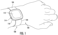
- Example aspects of the present disclosure are directed to a wearable device that can be worn, for instance, on a user's wrist or other location on the user's body.
- the wearable device can include an antenna, a conductive housing (e.g., a metal housing), a circuit board (e.g., a printed circuit board) located within the conductive housing, a cover (e.g., a plastic cover), and a label including film and a parasitic element.
- the antenna can be a slot antenna defined by a gap (e.g., a 0.1 mm gap to about a 5 mm gap) between the conductive housing and the printed circuit board.
- the slot antenna can have a signal that operates at a plurality of different frequency bands.
- the slot antenna can operate at one or more global navigation satellite system (GNSS) (e.g., global positioning system (GPS), GLONASS, Galileo, etc.) frequency bands.
- GNSS global navigation satellite system
- the one or more global navigation satellite system frequency bands can include one or more GPS frequency bands (e.g., 1164 MHz to 1189 MHz, 1563 MHz to 1587 MHz, 1215 MHz to 1240 MHz,).
- the wearable device since the wearable device must be compact enough to be worn, for instance, on the user's wrist, the distance of the antenna from the user's wrist may be small, which can, in some circumstances, impact the performance (e.g., radiation efficiency) of the slot antenna at the one or more GPS frequency bands. Specifically, there can be a tendency for too much signal to radiate through the cover directly into the user's wrist, which can negatively affect GPS performance.
- the parasitic element can be applied as one of a series of layers that are printed onto to a film that surrounds the outer surface of the cover of the wearable device, thereby forming a label.
- the film e.g., a transparent in molded label (IML) film
- parasitic element, and other layers of the label can then be stamped, formed to the shape of the outer surface of the cover, and insert molded onto the outer surface of the cover to provide a thin design where the parasitic element is close to the user's wrist and further from the system ground (e.g., at PCB 300) to improve antenna performance.
- the label including the parasitic element can have a thickness T (see FIG.
- the decorative ink layer is visible from the exterior of the wearable device through the transparent film, and the masking ink layer is utilized to hide the other layers of the label, such as the conductive ink layer that forms the parasitic element.
- the insulating ink layer(s) can add electrical stability to the parasitic element, and the gloss ink layer(s) can protect the conductive ink layer and the decorative ink layer from hot plastic during the insert molding process in which the various layers of the label including the parasitic element are joined to a plastic bottom cover of the wearable device. Further, the bonding layer bonds the label to the exterior surface of the plastic cover.
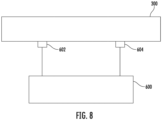
- the parasitic element can be electrically connected to the printed circuit board.
- the parasitic element can be electrically connected to a ground plane of the printed circuit board.
- the parasitic element can be direct current (DC) grounded to the printed circuit board at a first location thereon.
- the parasitic element can be DC grounded to the printed circuit board at a second location thereon. The first location and the second location can be spaced apart from one another along the printed circuit board.
- the printed circuit board can include a first fastener (e.g., spring clip, booster pin, compression spring, etc.) at the first location and a second fastener (e.g., spring clip, booster pin, compression spring, etc.) at the second location to couple the parasitic element to the printed circuit board via a first opening and a second opening at the first location and the second location, respectively.
- a first contact of the parasitic element and/or a second contact of the parasitic element can be mechanically coupled and/or electrically coupled to the printed circuit board via the first fastener and the second fastener, respectively, rather than via a solder connection.
- the parasitic element can be electrically grounded to the printed circuit board.
- the parasitic element can be RF grounded to the printed circuit board multiple locations.
- the antenna e.g., a slot antenna
- the parasitic element can improve the radiation efficiency of the antenna at the one or more frequency bands by at least about 2 decibels, such as by at least about 3 decibels, such as by at least about 4 decibels.
- the one or more input devices 114 can be manipulated to control operation of a backlight (not shown) associated with the display 112. It should be understood that the one or more input devices 114 can be configured to allow the user to interact with the wearable device 100 in any suitable manner. For instance, in some implementations, the one or more input devices 114 can be manipulated by the user to navigate through one or more menus on the display 112.
- the conductive housing 120 can include any suitable conductive material.
- the conductive housing 120 can include a metal housing.
- the bottom cover 122 can include an insulating material.
- the bottom cover 122 can include a plastic cover.
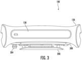
- FIG. 3 depicts a side view of the wearable device 100 with the bottom cover 122 ( FIG. 2 ) removed.
- FIG. 4 depicts a side view of the wearable device 100 with the housing assembly 110 ( FIG. 2 ) removed.
- the display 112 can, in some implementations, include display traces (e.g., ITO coating) 116 and touch traces (e.g., ITO coating) 118.
- the wearable device 100 can also include one or more electrodes 124 to collect and store data regarding any number of parameters (electrodermal activity, etc.) that can be communicated to the user.
- the printed circuit board 300 can include one or more charging pins 304.
- the wearable device 100 can be coupled to a charging circuit (not shown) via the one or more charging pins 304 to facilitate charging of an energy storage device (e.g., battery) of the wearable device 100.
- an energy storage device e.g., battery
- the conductive housing 120 can define an opening (e.g., cutout) for one or more electrodes 124. In this manner, the one or more electrodes 124 can be visible to the user.
- the one or more electrodes 124 can include an electrodermal activity (EDA) electrode.
- EDA electrodermal activity
- the user can contact (e.g., touch) the one or more electrodes 124 to facilitate measuring one or more health metrics (e.g., heart-rate, blood pressure,, EDA etc.) of the user.
- health metrics e.g., heart-rate, blood pressure,, EDA etc.
- the slot antenna 500 can be operable at a plurality of different frequency bands.
- the slot antenna 500 can be operable at one or more Global Navigation Satellite System (GNSS) frequency bands.
- GNSS Global Navigation Satellite System
- the one or more GNSS frequency bands can include one or more GPS frequency bands.
- the one or more GPS frequency bands can include at least one of a first GPS frequency band ranging from about 1164 Megahertz (MHz) to about 1189 MHz, a second GPS frequency band ranging from about 1563 MHz to about 1587 MHz, and a third GPS frequency band ranging from about 1215 MHz to about 1240 MHz.
- the slot antenna 500 can include a first grounding contact 502 and a second grounding contact 504.
- the first grounding contact 502 can couple the conductive housing 120 to the ground of the printed circuit board 300 at a first location.
- the second grounding contact 504 can couple the conductive housing 120 to the ground of the printed circuit board 300 at a second location.
- the first location and the second location can correspond to opposing sides of the printed circuit board 300.
- the first grounding contact 502 and the second grounding contact 504 can be coupled to the ground of the printed circuit board 300 at any suitable location to adjust a length of the slot antenna 500.
- the first grounding contact 502 and the second grounding contact 504 can be positioned to shorten the slot antenna 500.
- the first grounding contact 502 and the second grounding contact 504 can be positioned to lengthen the slot antenna 500.
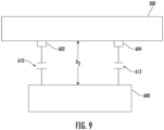
- the parasitic element 600 can be coupled to the printed circuit board 300 via one or more matching circuits.
- the parasitic element 600 can be RF grounded to the printed circuit board 300 at the first location 602 thereon via a first RF bypass capacitor 610.
- the parasitic element 600 can be RF grounded to the printed circuit board 300 at the second location 604 thereon via a second RF bypass capacitor 612.
- the RF bypass capacitors e.g., first RF bypass capacitor 610 and second RF bypass capacitor 612
- the parasitic element 600 can leave the parasitic element 600 electrically isolated to electrical ground at direct current and low frequencies (e.g., non-RF frequencies).
- the parasitic element 600 can be coupled to the printed circuit board at the first location 602 through a first matching circuit that can consist of one or more inductors and capacitors. Additionally, the parasitic element 600 can be coupled to the printed circuit board 300 at the second location 604 through a second matching circuit that can consist of one or more inductors and capacitors.
- the printed circuit board 300 can include a first fastener (e.g., spring clip) at the first location 602 thereon and a second fastener at the second location thereon.
- a first fastener e.g., spring clip
- the parasitic element 600 can be mechanically coupled to the printed circuit board 300 at the first location 602 and the second location 604 via the first fastener and the second fastener, respectively, as discussed in more detail below.
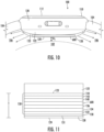
- the parasitic element is positioned a distance D1 away from the user's wrist 102.
- the distance D1 between the parasitic element 600 and the user's wrist 102 can range from about 0.15 millimeters to about 2.5 millimeters, such as from about 0.2 millimeters to about 2.25 millimeters, such as from about 0.25 millimeters to about 2 millimeters in order to improve the radiation efficiency of the slot antenna 500 of the wearable device 100.
- each layer described hereafter can itself include more than one layer, such as 2 or more layers, such as 3 more layers, such as 4 or more layers.
- each layer can be comprised of 2 to 10 layers, while in other embodiments, each layer may include only 1 individual layer.
- the overall resistance across the length of the parasitic element 600 can be less than about 2.5 Ohms, such as less than about 1.5 Ohms, such as less than about 1 Ohm.
- a decorative ink layer 130 can be applied to the film 128. Because the film 128 is transparent, the decorative ink layer 130 can be visible to a user or viewer from the bottom 129 of the wearable device 100. It should be understood that the decorative ink layer 130 may only be printed or applied to a portion of the film 128 depending on the particular designs, text, etc. that it is desired for a user or other viewer of the wearable device 100 to see. Any suitable ink of any desired color can be used for the decorative ink layer 130, with the understanding that the decorative ink layer 130 is non-conductive.
- a first gloss layer 134 can be applied on top of the non-conductive masking ink layer 132.
- the first gloss layer 134 can include four separate gloss layers.
- the first gloss layer 134 can be used to protect any of the various layers of the label 150 from heat damage when the label 150 is applied to the bottom cover 122 via insert molding.
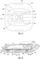
- the first gloss layer 134 can be completely transparent. Additionally, the first gloss layer 134 may not be applied on top of the entire inner surface 131 of the film 128 and any intervening layers because, as discussed in more detail below, various openings 125 may be needed for facilitating external charging of the wearable device 100 or where openings 126 may be needed to be expose where sensors 127 may be placed (see FIGs. 12-14 ).
- a first insulating ink layer 136 can be applied on top of the first gloss layer 134.
- the first insulating ink layer 136 (as well as the second insulating ink layer 140 discussed below) can be used to sandwich and protect the parasitic element 600, which is a conductive ink layer or layers, from interference with the other layers of the label 150.
- the first insulating ink layer 136 can be a dielectric ink. In some embodiments, the first insulating ink layer 136 can be completely transparent.
- the first insulating ink layer 136 can include from about 40 wt.% to about 90 wt.%, such as from about 45 wt.% to about 85 wt.%, such as from about 50 wt.% to about 50 wt.% of a glycol ether based on the total weight of the first insulating ink layer 136.
- the glycol ether can be diethylene glycol ethyl acetate, although it should be understood that any other suitable glycol ethers can be used as known to one of ordinary skill in the art.
- first insulating ink layer 136 may not be applied on top of the entire inner surface 131 of the film 128 and any intervening layers because, as discussed in more detail below, various openings 125 may be needed for facilitating external charging of the wearable device 100 or where openings 126 may be needed to be expose where sensors 127 may be placed (see FIGs. 12-14 ).
- a conductive ink layer that forms the parasitic element 600 can be applied thereon.
- the conductive ink layer can be metallic and serves as the parasitic element 600 that facilitates the enhancement of the slot antenna 500 of the wearable device 100 resulting in stronger RF signals 106.
- the conductive ink layer that forms the parasitic element 600 can include two separate conductive ink layers.
- the conductive ink layer can be a metallic paste.
- the conductive ink layer can include silver, copper, gold, aluminum, cobalt, nickel, tungsten, zinc, rhodium, iridium, ruthenium, osmium, palladium, platinum, or a combination thereof.
- a second insulating ink layer 140 can be applied on top of the conductive ink layer that forms the parasitic element 600.
- the second insulating ink layer 140 (as well as the first insulating ink layer 136 discussed above) can be used to sandwich and protect the conductive ink layer forming the parasitic element 600 from interference with the other layers of the label 150.
- the second insulating ink layer 140 can be a dielectric ink. In some embodiments, the second insulating ink layer 140 can be completely transparent.
- the bonding layer 144 may not be applied over a portion of the conductive ink layer and any intervening layers so that the resistance of the parasitic element 600 can be measured at one or more exposed sections 624 after injection molding of the plastic cover 122 and prior to final assembly of the wearable device 100 and so that the conductive ink layer forming the parasitic element 600 can be electrically connected to the printed circuit board 300 at one or more exposed sections 626 (see FIG. 12 ).
Landscapes
- Engineering & Computer Science (AREA)
- Physics & Mathematics (AREA)
- General Physics & Mathematics (AREA)
- Computer Hardware Design (AREA)
- Microelectronics & Electronic Packaging (AREA)
- Theoretical Computer Science (AREA)
- Support Of Aerials (AREA)
- Details Of Aerials (AREA)
- Aerials With Secondary Devices (AREA)
- Transceivers (AREA)
Priority Applications (1)
| Application Number | Priority Date | Filing Date | Title |
|---|---|---|---|
| EP25159708.4A EP4535570A3 (de) | 2022-05-19 | 2022-05-19 | Leitfähiges tintenbasiertes parasitäres element für eine geräteantenne |
Applications Claiming Priority (3)
| Application Number | Priority Date | Filing Date | Title |
|---|---|---|---|
| PCT/CN2022/093823 WO2023221035A1 (en) | 2022-05-19 | 2022-05-19 | Conductive ink-based parasitic element for a device antenna |
| EP25159708.4A EP4535570A3 (de) | 2022-05-19 | 2022-05-19 | Leitfähiges tintenbasiertes parasitäres element für eine geräteantenne |
| EP22888610.7A EP4298689A4 (de) | 2022-05-19 | 2022-05-19 | Leitfähiges tintenbasiertes parasitäres element für eine geräteantenne |
Related Parent Applications (1)
| Application Number | Title | Priority Date | Filing Date |
|---|---|---|---|
| EP22888610.7A Division EP4298689A4 (de) | 2022-05-19 | 2022-05-19 | Leitfähiges tintenbasiertes parasitäres element für eine geräteantenne |
Publications (2)
| Publication Number | Publication Date |
|---|---|
| EP4535570A2 true EP4535570A2 (de) | 2025-04-09 |
| EP4535570A3 EP4535570A3 (de) | 2025-06-18 |
Family
ID=88834279
Family Applications (2)
| Application Number | Title | Priority Date | Filing Date |
|---|---|---|---|
| EP22888610.7A Pending EP4298689A4 (de) | 2022-05-19 | 2022-05-19 | Leitfähiges tintenbasiertes parasitäres element für eine geräteantenne |
| EP25159708.4A Pending EP4535570A3 (de) | 2022-05-19 | 2022-05-19 | Leitfähiges tintenbasiertes parasitäres element für eine geräteantenne |
Family Applications Before (1)
| Application Number | Title | Priority Date | Filing Date |
|---|---|---|---|
| EP22888610.7A Pending EP4298689A4 (de) | 2022-05-19 | 2022-05-19 | Leitfähiges tintenbasiertes parasitäres element für eine geräteantenne |
Country Status (7)
| Country | Link |
|---|---|
| US (1) | US12314795B2 (de) |
| EP (2) | EP4298689A4 (de) |
| JP (1) | JP2025517739A (de) |
| KR (1) | KR20250005242A (de) |
| CN (1) | CN119213628A (de) |
| TW (1) | TW202412385A (de) |
| WO (1) | WO2023221035A1 (de) |
Family Cites Families (20)
| Publication number | Priority date | Publication date | Assignee | Title |
|---|---|---|---|---|
| AU5917499A (en) * | 1998-09-11 | 2000-04-03 | Alexander Gelbman | Smart electronic label employing electronic ink |
| JP5101318B2 (ja) * | 2008-01-28 | 2012-12-19 | グンゼ株式会社 | 乾燥装置、及び乾燥方法 |
| JP2010066045A (ja) * | 2008-09-09 | 2010-03-25 | Casio Comput Co Ltd | 電波受信装置 |
| US20100060459A1 (en) | 2008-09-11 | 2010-03-11 | IP B.V.Strawinskylaan | Rfid tag |
| FI20115072A0 (fi) | 2011-01-25 | 2011-01-25 | Pulse Finland Oy | Moniresonanssiantenni, -antennimoduuli ja radiolaite |
| JP5998795B2 (ja) * | 2012-09-24 | 2016-09-28 | セイコーエプソン株式会社 | アンテナ内蔵式電子時計 |
| JP5907479B2 (ja) * | 2013-03-22 | 2016-04-26 | カシオ計算機株式会社 | アンテナ装置及び電子機器 |
| CN105515599A (zh) * | 2014-09-30 | 2016-04-20 | 深圳富泰宏精密工业有限公司 | 无线通信装置 |
| JP6459593B2 (ja) * | 2015-02-13 | 2019-01-30 | セイコーエプソン株式会社 | アンテナ装置及び電子時計 |
| TWI659678B (zh) | 2015-09-15 | 2019-05-11 | 大陸商東莞錢鋒特殊膠黏製品有限公司 | 行動電子裝置之天線複合成型結構及其製作方法 |
| CN205177994U (zh) | 2015-11-06 | 2016-04-20 | 乐视移动智能信息技术(北京)有限公司 | 一种天线系统 |
| WO2018016574A1 (ja) * | 2016-07-20 | 2018-01-25 | シチズン時計株式会社 | 携帯型電波時計 |
| US20180028072A1 (en) * | 2016-07-29 | 2018-02-01 | VivaLnk, Inc. | Wearable thermometer patch capable of measuring human skin temperature at high duty cycle |
| WO2018068190A1 (zh) | 2016-10-10 | 2018-04-19 | 华为技术有限公司 | 一种可穿戴设备 |
| CN110036349B (zh) * | 2017-02-16 | 2024-01-30 | 华为技术有限公司 | 一种可穿戴设备 |
| TWI645688B (zh) * | 2017-07-11 | 2018-12-21 | 巨擘科技股份有限公司 | 穿戴式裝置及其操作方法 |
| TWI638485B (zh) * | 2017-10-05 | 2018-10-11 | 廣達電腦股份有限公司 | 穿戴式裝置 |
| US10992029B2 (en) * | 2018-12-13 | 2021-04-27 | Fitbit, Inc. | Multiple band antenna structures |
| CN114444643B (zh) | 2019-04-17 | 2024-08-06 | 苹果公司 | 无线可定位标签 |
| US10839171B2 (en) | 2019-04-22 | 2020-11-17 | Apple Inc. | Integrated sensing tag-based wireless sensing within electronic devices |
-
2022
- 2022-05-19 JP JP2024568290A patent/JP2025517739A/ja active Pending
- 2022-05-19 KR KR1020247037350A patent/KR20250005242A/ko active Pending
- 2022-05-19 WO PCT/CN2022/093823 patent/WO2023221035A1/en not_active Ceased
- 2022-05-19 EP EP22888610.7A patent/EP4298689A4/de active Pending
- 2022-05-19 EP EP25159708.4A patent/EP4535570A3/de active Pending
- 2022-05-19 CN CN202280096054.5A patent/CN119213628A/zh active Pending
- 2022-05-19 US US18/251,772 patent/US12314795B2/en active Active
-
2023
- 2023-05-05 TW TW112116716A patent/TW202412385A/zh unknown
Also Published As
| Publication number | Publication date |
|---|---|
| EP4298689A4 (de) | 2024-05-29 |
| EP4535570A3 (de) | 2025-06-18 |
| US12314795B2 (en) | 2025-05-27 |
| US20240354546A1 (en) | 2024-10-24 |
| KR20250005242A (ko) | 2025-01-09 |
| WO2023221035A1 (en) | 2023-11-23 |
| EP4298689A1 (de) | 2024-01-03 |
| TW202412385A (zh) | 2024-03-16 |
| JP2025517739A (ja) | 2025-06-10 |
| CN119213628A (zh) | 2024-12-27 |
Similar Documents
| Publication | Publication Date | Title |
|---|---|---|
| TWI568329B (zh) | 利用電連接至器件外殼構件之天線結構 | |
| EP1451897B1 (de) | Vhf-wellenempfängerantenne, die in einem armband einer tragbaren elektronischen einrichtung untergebracht ist | |
| US10461404B2 (en) | Terminal housing and terminal | |
| US8717240B2 (en) | Multi-angle ultra wideband antenna with surface mount technology | |
| US9152833B2 (en) | Antenna circuit | |
| JPH11177327A (ja) | 逆fアンテナ装置 | |
| EP4145631A1 (de) | Wearable-vorrichtung | |
| US12314795B2 (en) | Conductive ink-based parasitic element for a device antenna | |
| CN110994137A (zh) | 穿戴电子设备 | |
| KR101643928B1 (ko) | 안테나 구조체 | |
| CN114488767A (zh) | 可穿戴设备以及智能手表 | |
| EP4338232B1 (de) | Tragbare computervorrichtung mit mehrbandschlitzantenne und geerdetem parasitärem element | |
| CN112886206B (zh) | 穿戴式电子设备 | |
| KR101651902B1 (ko) | 안테나 구조체의 제조 방법 | |
| JP5873350B2 (ja) | アンテナ一体型無線モジュール | |
| CN112886212B (zh) | 穿戴式电子设备 | |
| FI20205799A1 (en) | COVER AND MODULE FOR WEARABLE SMALL RF DEVICE AND WEARABLE RF DEVICE | |
| CN121125895A (zh) | 一种电子设备 | |
| CN109462418B (zh) | 可穿戴设备 | |
| KR20170089482A (ko) | 손목시계 형태의 전자 장치 |
Legal Events
| Date | Code | Title | Description |
|---|---|---|---|
| PUAI | Public reference made under article 153(3) epc to a published international application that has entered the european phase |
Free format text: ORIGINAL CODE: 0009012 |
|
| STAA | Information on the status of an ep patent application or granted ep patent |
Free format text: STATUS: THE APPLICATION HAS BEEN PUBLISHED |
|
| AC | Divisional application: reference to earlier application |
Ref document number: 4298689 Country of ref document: EP Kind code of ref document: P |
|
| AK | Designated contracting states |
Kind code of ref document: A2 Designated state(s): AL AT BE BG CH CY CZ DE DK EE ES FI FR GB GR HR HU IE IS IT LI LT LU LV MC MK MT NL NO PL PT RO RS SE SI SK SM TR |
|
| REG | Reference to a national code |
Ref country code: DE Ref legal event code: R079 Free format text: PREVIOUS MAIN CLASS: H01Q0019100000 Ipc: H01Q0001270000 |
|
| PUAL | Search report despatched |
Free format text: ORIGINAL CODE: 0009013 |
|
| AK | Designated contracting states |
Kind code of ref document: A3 Designated state(s): AL AT BE BG CH CY CZ DE DK EE ES FI FR GB GR HR HU IE IS IT LI LT LU LV MC MK MT NL NO PL PT RO RS SE SI SK SM TR |
|
| RIC1 | Information provided on ipc code assigned before grant |
Ipc: H01Q 19/10 20060101ALI20250509BHEP Ipc: H01Q 13/10 20060101ALI20250509BHEP Ipc: H01Q 1/44 20060101ALI20250509BHEP Ipc: H01Q 1/27 20060101AFI20250509BHEP |
|
| STAA | Information on the status of an ep patent application or granted ep patent |
Free format text: STATUS: REQUEST FOR EXAMINATION WAS MADE |
|
| 17P | Request for examination filed |
Effective date: 20251217 |
|
| GRAP | Despatch of communication of intention to grant a patent |
Free format text: ORIGINAL CODE: EPIDOSNIGR1 |
|
| STAA | Information on the status of an ep patent application or granted ep patent |
Free format text: STATUS: GRANT OF PATENT IS INTENDED |
|
| INTG | Intention to grant announced |
Effective date: 20260226 |