EP4535178A2 - Codage de données au moyen d'une combinasion dún masque de données et d'une inversion de bus de données - Google Patents
Codage de données au moyen d'une combinasion dún masque de données et d'une inversion de bus de données Download PDFInfo
- Publication number
- EP4535178A2 EP4535178A2 EP25153229.7A EP25153229A EP4535178A2 EP 4535178 A2 EP4535178 A2 EP 4535178A2 EP 25153229 A EP25153229 A EP 25153229A EP 4535178 A2 EP4535178 A2 EP 4535178A2
- Authority
- EP
- European Patent Office
- Prior art keywords
- data
- circuit
- mask signal
- encoded
- bit
- Prior art date
- Legal status (The legal status is an assumption and is not a legal conclusion. Google has not performed a legal analysis and makes no representation as to the accuracy of the status listed.)
- Pending
Links
Images



Classifications
-
- G—PHYSICS
- G06—COMPUTING OR CALCULATING; COUNTING
- G06F—ELECTRIC DIGITAL DATA PROCESSING
- G06F13/00—Interconnection of, or transfer of information or other signals between, memories, input/output devices or central processing units
- G06F13/38—Information transfer, e.g. on bus
- G06F13/42—Bus transfer protocol, e.g. handshake; Synchronisation
- G06F13/4265—Bus transfer protocol, e.g. handshake; Synchronisation on a point to point bus
Definitions
- the present disclosure relates to encoding data for transfer on a chip to chip communication link.
- Integrated circuit devices communicate with one another using input/output (I/O) circuits that are configured to transmit and receive multi-bit data over a plurality of signal lines.
- I/O input/output
- SSO simultaneous switching output
- SSN simultaneous switching noise
- DBI data bus inversion
- DBI dynamic bus inversion
- a data mask (dm) signal is used by one circuit to indicate to another circuit that the data sent by the one circuit should be disregarded by the other circuit.
- the data mask signal may be used by a memory controller to indicate to a memory device that the data transmitted by the memory controller to the memory device should be ignored.
- the data mask signal can be a voltage level on a pin of the memory controller integrated circuit or part of a command transmitted between the memory controller and the memory device.
- Embodiments of the present disclosure include a data encoding scheme for transmission of data from one circuit to another circuit that combines DBI encoding and non-DBI encoding and uses a data mask signal to indicate the type of encoding used.
- non-DBI encoding is used to refer to any encoding scheme that is different from DBI.
- the data mask signal in a first state indicates that the data transmitted from one circuit to said another circuit is to be ignored, and the data mask signal in a second state indicates that the data transmitted from one circuit to said another circuit is not to be ignored. If the data mask signal is in the second state, a first subset of the data is encoded with data bus inversion and a second subset of the data is encoded differently from data bus inversion.
- the encoding scheme according to the embodiments described herein has the advantage that SSO noise can be dramatically reduced when the encoded data is transmitted from one circuit to another circuit.
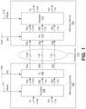
- encoder 106 also receives a mode signal 116.
- mode signal 116 when mode signal 116 is asserted (e.g., logic high), encoder 106 encodes the n-bit data D n using the encoding scheme according to the embodiments of the present disclosure as described herein.
- mode signal 116 When mode signal 116 is not asserted (c.g., logic low), encoder 106 uses DBI encoding (that is independent of the use of masking information) to encode the n-bit data D n .
- Receiver 110 provides the received encoded data DQ n , DBI bit, and the DM bit to decoder 112.
- Decoder 112 decodes the encoded data DQ n and DBI bit back to n-bit data D n and converts the modified data mask signal (DM) back to the data mask signal (dm), as will be explained in more detail below with reference to FIGS. 4 and 5 .
- decoder 112 also receives a mode signal 516.
- mode signal 516 when mode signal 516 is asserted (e.g., logic high), decoder 112 decodes the n-bit encoded data DQ n using the decoding scheme according to the embodiments of the present disclosure as described herein.
- mode signal 516 is not asserted (i.e., logic low)
- decoder logic 112 uses DBI decoding (that is independent of the use of masking information) to decode the n-bit encoded data DQ n .
- step 206 it is further determined whether the n-bit data D n , when DBI encoded, has a Hamming Weight lower than a predetermined threshold. In other words, in step 206 it is further determined whether the uncoded n-bit data D n has a Hamming Weight lower than a first predetermined threshold or higher than a second predetermined threshold.
- a threshold of Hamming Weight 3 may be used such that the 8-bit data D n is considered low Hamming Weight data if the 8-bit data D n , when DBI encoded, has Hamming Weight lower than 4 (i.e., HW of DBI-encoded D n is 0, 1, 2, or 3), i.e., when the uncoded 8-bit data D n has Hamming Weight lower than 4 (i.e., HW of uncoded D n is 0, 1, 2, or 3) or higher than 5 (i.e., HW of uncoded D n is 6, 7, or 8).
- Table 1 illustrates an example of combinatorial logic that may be used to encode 8-bit input data D n to 9-bit encoded data [DBI, DQ n ] according to the embodiment as shown in FIG. 2 .
- the combinatorial logic shown in Table 1 is merely exemplary, and other combinatorial logic may be used to perform the encoding as illustrated in FIG. 2 .
- the encoded data [DBI, DQ n ] is DQM (111000000).
- data D n with Hamming Weights of 4 or 5 are encoded using DBI such that the data bits of data D n with Hamming Weight of 4 are not inverted and the DBI bit is set to 0 while the data bits of data D n with Hamming Weight of 5 are inverted and the DBI bit is set to 1.
- the DBI-encoded data [DBI, DQ n ] has Hamming Weight of 4 only.
- 8-bit data pattern in the form of 00000000 with HW of zero is encoded to the 9-bit encoded data pattern 101010000 with HW of three.
- 8-bit data in the form of x 7 x 6 x 5 x 4 0000 with HW of one are encoded into 9-bit data in the form of 0 1000 x 7 x 6 x 5 x 4 with HW of four
- 8-bit data patterns in the form of 0000 x 3 x 2 x 1 x 0 with HW of one are encoded to 9-bit encoded data patterns in the form of 00100 x 3 x 2 x 1 x 0 with HW of four, where x n is the n-th bit from a least significant bit of the 8-bit data pattern and x n is the complement of x n .
- 8-bit data patterns in the form of 00 x 5 x 4 x 3 x 2 x 1 x 0 with HW of two are encoded to 9-bit encoded data patterns in the form of 011 x 5 x 4 x 3 x 2 x 1 x 0 with HW of four
- 8-bit data patterns in the form of 01 x 5 x 4 x 3 x 2 x 1 x 0 with HW of two are encoded to 9-bit encoded data patterns in the form of 0101 0 y 3 y 2 y 1 y 0 with HW of four
- 8-bit data patterns in the form of 10 x 5 x 4 x 3 x 2 x 1 x 0 with HW of two are encoded to 9-bit encoded data patterns in the form of 01001 y 3 y 2 y 1 y 0 with HW of four
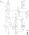
- data mask signal (dm) 312 when data mask signal (dm) 312 is asserted ("1" or logic high), the modified data mask signal DM 326 output from OR gate 314 is also "1" or logic high.
- data mask signal (dm) 312 also causes multiplexer 310 to select the predetermined bit pattern DQM 323 as its output 316.
- the output 324 of AND gate 312 becomes logic low if the input data D n , when DBI-encoded by DBI encoder 302, has a Hamming Weight not lower than a predetermined threshold and thus the low HW signal 306 is not asserted.
- multiplexer 308 selects the output 318 of DBI encoder 302 as its output 322.
- the modified data mask signal DM 326 at logic low can indicate to the memory device 104 that DBI encoding has been used to encode the input data D n .
- the modified data mask signal (DM) is asserted ("1" or logic high). If the modified data mask signal (DM) is not asserted, that means the data [DBI, DQ n ] was DBI-encoded (step 210 of FIG. 2 ). Thus, data [DBI, DQ n ] is decoded using DBI and the data mask signal (dm) is set to "0" to indicate that the decoded data D n should not be ignored. On the other hand, if the modified data mask (DM) signal is not asserted, then it is further determined 406 whether the encoded data [DBI, DQ n ] matches the predetermined data pattern DQM.
- decoding of the data [DBI, DQ n ] can be performed simply by reversing the combinatorial logic used to encode the data DQ n .
- the 9-bit data [DBI, DQ n ] can be decoded to recover the 8-bit data DQ n simply by reversing the combinatorial logic shown in Table 1.
- 9-bit data in the form of 0 1000 x 7 x 6 x 5 x 4 with HW of four can be decoded into 8 bit data x 7 x 6 x 5 x 4 0000 with HW of one.
- Numerous other examples of reversing the combinatorial logic for decoding are apparent from Table 1.
- such reverse mappings of logic may also be predetermined and stored in a LUT.
- the decoder circuit 112 when the modified data mask signal (DM) 512 is not asserted ("0" or logic low), that means that the data [DBI, DQ n ] was DBI-encoded (step 210 of FIG. 2 ).
- the data mask signal (dm) 532 output from AND gate 530 is set at logic low ("0").
- the output 508 of AND gate 506 is also at logic low, thereby causing multiplexer 510 to select the output 518 of DBI decoder 502 as its output DQ n 522.
- the data [DBI, DQ n ] is decoded using DBI (step 404 of FIG. 4 ).
- the output data mask signal (dm) 532 of AND gate 530 is at logic high if the output 524 of comparator 512 is at logic high, i.e., when the encoded data [DBI, DQ n ] matches the predetermined data pattern DQM as in step 406 of FIG. 4 .
- data mask signal (dm) 532 is at logic high, the encoded data is disregarded (step 408 of FIG. 4 ).
- mode signal 516 is at logic low (“0")
- the output 508 of AND gate 506 is also always at logic low regardless of the state of the modified data mask signal (DM) 512, thereby causing multiplexer 510 to always select the output 518 of DBI decoder 502 as its output DQ n 522.
- the output 528 of OR gate 526 is always at logic high if mode signal 516 is at logic low, and thus the data mask signal (dm) 532 output from AND gate 530 follows the state of the modified data mask signal (DM) 512.
- the data [DBI, DQ n ] is always decoded using DBI decoding when mode signal 516 is not asserted.
- FIG. 6A illustrates Hamming Weights (HWs) present in 9 bit data including 8 bit uncoded data and a DBI bit
- FIG. 6B illustrates Hamming Weights present in 9 bit coded data including a DBI bit and 8 bit coded data encoded according to one embodiment.
- HWs Hamming Weights
- the HW histogram illustrates the distribution of HWs in the 9-bit data including DBI (1 bit) and 8 bit uncoded data, and the HW histograms 602 when such uncoded 9 bit data is encoded using conventional DBI ([DBI + 8 bit DBI-encoded data]).
- Table 2 shows the current (Idd) that would be drawn by transmitter (Tx) 108 ( FIG. 1 ) when the data D n is transmitted uncoded, conventional DBI-coded, and coded with combined DM/DBI according to the embodiments herein, referencing the supply current Idd to be drawn when data D n is transmitted uncoded as the reference (100%).
- Table 2 Idd Uncoded Conventional DBI Combined DM/DBI Coded Idd, DC-peak (%) 100% 50% 50% Idd, DC-average (%) 100% 40% 45% Idd, AC peak-peak (%) 100% 50% 25% Idd, AC rms (%) 100% 61% 13%
- the AC supply current drawn from the power supply is reduced dramatically, from 50% to 25% for AC peak-to-peak supply current Idd and from 61% to 13% for AC rms (root-mean-square) values, when the combined DM/DBI encoding scheme according to the embodiments described herein is used, compared to conventional DBI encoding.
- SSO noise can be dramatically reduced when using the combined DM/DBI encoding scheme according to the embodiments described herein.
Landscapes
- Engineering & Computer Science (AREA)
- Theoretical Computer Science (AREA)
- Physics & Mathematics (AREA)
- General Engineering & Computer Science (AREA)
- General Physics & Mathematics (AREA)
- Dram (AREA)
- Dc Digital Transmission (AREA)
- Error Detection And Correction (AREA)
- Compression, Expansion, Code Conversion, And Decoders (AREA)
Applications Claiming Priority (7)
| Application Number | Priority Date | Filing Date | Title |
|---|---|---|---|
| US22510209P | 2009-07-13 | 2009-07-13 | |
| EP20100800221 EP2454672B1 (de) | 2009-07-13 | 2010-06-14 | Datenverschlüsselung über eine kombination aus einer datenmaske und einer datenbus-umkehrung |
| EP17153209.6A EP3193259B1 (de) | 2009-07-13 | 2010-06-14 | Datenverschlüsselung über eine kombination aus einer datenmaske und einer datenbus-umkehrung |
| EP15151769.5A EP2894571B1 (de) | 2009-07-13 | 2010-06-14 | Datenverschlüsselungs über eine Kombination aus einer Datenmaske und einer Datenbus-Umkehrung |
| EP19215923.4A EP3654191B1 (de) | 2009-07-13 | 2010-06-14 | Datenverschlüsselung über eine kombination aus einer datenmaske und einer datenbus-umkehrung |
| EP23175716.2A EP4224328B1 (de) | 2009-07-13 | 2010-06-14 | Datenverschlüsselung über eine kombination aus einer datenmaske und einer datenbus-umkehrung |
| PCT/US2010/038556 WO2011008394A2 (en) | 2009-07-13 | 2010-06-14 | Encoding data using combined data mask and data bus inversion |
Related Parent Applications (6)
| Application Number | Title | Priority Date | Filing Date |
|---|---|---|---|
| EP23175716.2A Division-Into EP4224328B1 (de) | 2009-07-13 | 2010-06-14 | Datenverschlüsselung über eine kombination aus einer datenmaske und einer datenbus-umkehrung |
| EP23175716.2A Division EP4224328B1 (de) | 2009-07-13 | 2010-06-14 | Datenverschlüsselung über eine kombination aus einer datenmaske und einer datenbus-umkehrung |
| EP20100800221 Division EP2454672B1 (de) | 2009-07-13 | 2010-06-14 | Datenverschlüsselung über eine kombination aus einer datenmaske und einer datenbus-umkehrung |
| EP19215923.4A Division EP3654191B1 (de) | 2009-07-13 | 2010-06-14 | Datenverschlüsselung über eine kombination aus einer datenmaske und einer datenbus-umkehrung |
| EP17153209.6A Division EP3193259B1 (de) | 2009-07-13 | 2010-06-14 | Datenverschlüsselung über eine kombination aus einer datenmaske und einer datenbus-umkehrung |
| EP15151769.5A Division EP2894571B1 (de) | 2009-07-13 | 2010-06-14 | Datenverschlüsselungs über eine Kombination aus einer Datenmaske und einer Datenbus-Umkehrung |
Publications (2)
| Publication Number | Publication Date |
|---|---|
| EP4535178A2 true EP4535178A2 (de) | 2025-04-09 |
| EP4535178A3 EP4535178A3 (de) | 2025-06-18 |
Family
ID=43450053
Family Applications (6)
| Application Number | Title | Priority Date | Filing Date |
|---|---|---|---|
| EP25153229.7A Pending EP4535178A3 (de) | 2009-07-13 | 2010-06-14 | Codage de données au moyen d'une combinasion dún masque de données et d'une inversion de bus de données |
| EP19215923.4A Active EP3654191B1 (de) | 2009-07-13 | 2010-06-14 | Datenverschlüsselung über eine kombination aus einer datenmaske und einer datenbus-umkehrung |
| EP17153209.6A Active EP3193259B1 (de) | 2009-07-13 | 2010-06-14 | Datenverschlüsselung über eine kombination aus einer datenmaske und einer datenbus-umkehrung |
| EP23175716.2A Active EP4224328B1 (de) | 2009-07-13 | 2010-06-14 | Datenverschlüsselung über eine kombination aus einer datenmaske und einer datenbus-umkehrung |
| EP20100800221 Active EP2454672B1 (de) | 2009-07-13 | 2010-06-14 | Datenverschlüsselung über eine kombination aus einer datenmaske und einer datenbus-umkehrung |
| EP15151769.5A Active EP2894571B1 (de) | 2009-07-13 | 2010-06-14 | Datenverschlüsselungs über eine Kombination aus einer Datenmaske und einer Datenbus-Umkehrung |
Family Applications After (5)
| Application Number | Title | Priority Date | Filing Date |
|---|---|---|---|
| EP19215923.4A Active EP3654191B1 (de) | 2009-07-13 | 2010-06-14 | Datenverschlüsselung über eine kombination aus einer datenmaske und einer datenbus-umkehrung |
| EP17153209.6A Active EP3193259B1 (de) | 2009-07-13 | 2010-06-14 | Datenverschlüsselung über eine kombination aus einer datenmaske und einer datenbus-umkehrung |
| EP23175716.2A Active EP4224328B1 (de) | 2009-07-13 | 2010-06-14 | Datenverschlüsselung über eine kombination aus einer datenmaske und einer datenbus-umkehrung |
| EP20100800221 Active EP2454672B1 (de) | 2009-07-13 | 2010-06-14 | Datenverschlüsselung über eine kombination aus einer datenmaske und einer datenbus-umkehrung |
| EP15151769.5A Active EP2894571B1 (de) | 2009-07-13 | 2010-06-14 | Datenverschlüsselungs über eine Kombination aus einer Datenmaske und einer Datenbus-Umkehrung |
Country Status (5)
| Country | Link |
|---|---|
| US (1) | US8510490B2 (de) |
| EP (6) | EP4535178A3 (de) |
| JP (1) | JP5575237B2 (de) |
| ES (1) | ES2777777T3 (de) |
| WO (1) | WO2011008394A2 (de) |
Families Citing this family (29)
| Publication number | Priority date | Publication date | Assignee | Title |
|---|---|---|---|---|
| US8539301B2 (en) * | 2009-10-21 | 2013-09-17 | Nec Laboratories America, Inc. | Message-wise unequal error protection |
| EP2526492B1 (de) * | 2010-01-20 | 2016-01-06 | Rambus Inc. | Datenbusumkehr mit mehreren worten |
| KR101145317B1 (ko) * | 2010-04-29 | 2012-05-14 | 에스케이하이닉스 주식회사 | 데이터 전송회로 및 데이터 전송방법, 데이터 송/수신 시스템 |
| US8726139B2 (en) | 2011-12-14 | 2014-05-13 | Advanced Micro Devices, Inc. | Unified data masking, data poisoning, and data bus inversion signaling |
| KR20130098681A (ko) | 2012-02-28 | 2013-09-05 | 삼성전자주식회사 | 반도체 메모리 장치 |
| US9275692B2 (en) | 2012-02-28 | 2016-03-01 | Micron Technology, Inc. | Memory, memory controllers, and methods for dynamically switching a data masking/data bus inversion input |
| US9529749B2 (en) | 2013-03-15 | 2016-12-27 | Qualcomm Incorporated | Data bus inversion (DBI) encoding based on the speed of operation |
| US9252802B2 (en) | 2014-02-07 | 2016-02-02 | Qualcomm Incorporated | Encoding for partitioned data bus |
| US9148171B1 (en) * | 2014-07-29 | 2015-09-29 | Avago Technologies General Ip (Singapore) Pte. Ltd. | Parallel interface pattern modification for addressing signal integrity concerns |
| KR102201642B1 (ko) * | 2014-11-28 | 2021-01-13 | 삼성전자주식회사 | Puf 회로 및 그것의 키 등록 방법 |
| US9665527B2 (en) | 2014-12-09 | 2017-05-30 | Intel Corporation | Dynamic bus inversion with programmable termination level to maintain programmable target ratio of ones and zeros in signal lines |
| US20160173134A1 (en) * | 2014-12-15 | 2016-06-16 | Intel Corporation | Enhanced Data Bus Invert Encoding for OR Chained Buses |
| KR20160076889A (ko) * | 2014-12-23 | 2016-07-01 | 에스케이하이닉스 주식회사 | 반도체장치 및 반도체시스템 |
| US9922686B2 (en) | 2016-05-19 | 2018-03-20 | Micron Technology, Inc. | Apparatuses and methods for performing intra-module databus inversion operations |
| US10373657B2 (en) * | 2016-08-10 | 2019-08-06 | Micron Technology, Inc. | Semiconductor layered device with data bus |
| KR20180057028A (ko) * | 2016-11-21 | 2018-05-30 | 에스케이하이닉스 주식회사 | 데이터 반전 회로 |
| US10146719B2 (en) * | 2017-03-24 | 2018-12-04 | Micron Technology, Inc. | Semiconductor layered device with data bus |
| US10290289B2 (en) | 2017-04-01 | 2019-05-14 | Intel Corporation | Adaptive multibit bus for energy optimization |
| US10664432B2 (en) | 2018-05-23 | 2020-05-26 | Micron Technology, Inc. | Semiconductor layered device with data bus inversion |
| KR102638791B1 (ko) * | 2018-09-03 | 2024-02-22 | 에스케이하이닉스 주식회사 | 반도체장치 및 반도체시스템 |
| US10964702B2 (en) | 2018-10-17 | 2021-03-30 | Micron Technology, Inc. | Semiconductor device with first-in-first-out circuit |
| KR102767986B1 (ko) * | 2020-02-17 | 2025-02-14 | 에스케이하이닉스 주식회사 | 반도체장치 |
| US10944435B1 (en) * | 2020-03-27 | 2021-03-09 | Nxp B.V. | Tearing save encoding |
| KR102921871B1 (ko) * | 2020-12-17 | 2026-02-02 | 삼성전자주식회사 | 데이터 전송 방법 및 데이터 전송 장치 |
| KR20220140234A (ko) * | 2021-04-09 | 2022-10-18 | 삼성전자주식회사 | 멀티 레벨 신호 시스템에서 최적 전이 코드를 생성하기 위한 신호 처리 방법 및 반도체 장치 |
| US11720516B2 (en) | 2021-08-15 | 2023-08-08 | Apple Inc. | Methods for data bus inversion |
| KR102826989B1 (ko) * | 2021-08-26 | 2025-06-30 | 한양대학교 산학협력단 | Pam 4 신호를 이용하여 dbi-dc 인코딩을 수행하는 데이터 반전 회로 |
| KR102871891B1 (ko) * | 2021-08-26 | 2025-10-16 | 한양대학교 산학협력단 | Pam 4 신호를 이용하여 dbi-ac 인코딩을 수행하는 데이터 반전 회로 |
| US11836107B2 (en) | 2022-03-01 | 2023-12-05 | Apple Inc. | Power consumption control based on random bus inversion |
Family Cites Families (12)
| Publication number | Priority date | Publication date | Assignee | Title |
|---|---|---|---|---|
| JPH08316840A (ja) * | 1995-03-16 | 1996-11-29 | Toshiba Corp | 符号化装置および復号化装置 |
| US20020156953A1 (en) * | 2001-02-28 | 2002-10-24 | Beiley Mark A. | Dynamic bus inversion method |
| US6898648B2 (en) * | 2002-02-21 | 2005-05-24 | Micron Technology, Inc. | Memory bus polarity indicator system and method for reducing the affects of simultaneous switching outputs (SSO) on memory bus timing |
| KR100546335B1 (ko) * | 2003-07-03 | 2006-01-26 | 삼성전자주식회사 | 데이터 반전 스킴을 가지는 반도체 장치 |
| US7519892B1 (en) | 2005-10-14 | 2009-04-14 | Nvidia Corporation | Binary data encoding/decoding with error detection, such as for communicating between computing platform components |
| US7519893B2 (en) * | 2005-10-14 | 2009-04-14 | Nvidia Corporation | Binary data encoding/decoding for parallel bus |
| US7574647B1 (en) | 2005-10-14 | 2009-08-11 | Nvidia Corporation | Binary data encoding/decoding such as for communicating between computing platform components over a parallel interconnect |
| KR100877680B1 (ko) * | 2006-04-04 | 2009-01-09 | 삼성전자주식회사 | 반도체 장치 사이의 단일형 병렬데이터 인터페이스 방법,기록매체 및 반도체 장치 |
| JP2008099204A (ja) * | 2006-10-16 | 2008-04-24 | Toshiba Corp | 論理回路 |
| US7925844B2 (en) * | 2007-11-29 | 2011-04-12 | Micron Technology, Inc. | Memory register encoding systems and methods |
| US8363707B2 (en) * | 2008-03-21 | 2013-01-29 | Micron Technology, Inc. | Mixed-mode signaling |
| US8498344B2 (en) * | 2008-06-20 | 2013-07-30 | Rambus Inc. | Frequency responsive bus coding |
-
2010
- 2010-06-14 EP EP25153229.7A patent/EP4535178A3/de active Pending
- 2010-06-14 WO PCT/US2010/038556 patent/WO2011008394A2/en not_active Ceased
- 2010-06-14 EP EP19215923.4A patent/EP3654191B1/de active Active
- 2010-06-14 JP JP2012520647A patent/JP5575237B2/ja active Active
- 2010-06-14 US US13/378,939 patent/US8510490B2/en active Active
- 2010-06-14 EP EP17153209.6A patent/EP3193259B1/de active Active
- 2010-06-14 EP EP23175716.2A patent/EP4224328B1/de active Active
- 2010-06-14 EP EP20100800221 patent/EP2454672B1/de active Active
- 2010-06-14 ES ES17153209T patent/ES2777777T3/es active Active
- 2010-06-14 EP EP15151769.5A patent/EP2894571B1/de active Active
Also Published As
| Publication number | Publication date |
|---|---|
| JP2012533264A (ja) | 2012-12-20 |
| JP5575237B2 (ja) | 2014-08-20 |
| EP3654191C0 (de) | 2023-08-02 |
| EP4224328B1 (de) | 2025-03-12 |
| ES2777777T3 (es) | 2020-08-06 |
| US20120131244A1 (en) | 2012-05-24 |
| EP2454672A4 (de) | 2013-11-20 |
| WO2011008394A3 (en) | 2011-03-10 |
| EP4535178A3 (de) | 2025-06-18 |
| EP3654191A1 (de) | 2020-05-20 |
| US8510490B2 (en) | 2013-08-13 |
| EP2454672A2 (de) | 2012-05-23 |
| EP2454672B1 (de) | 2015-01-21 |
| EP3654191B1 (de) | 2023-08-02 |
| EP4224328A3 (de) | 2023-10-18 |
| EP3193259A1 (de) | 2017-07-19 |
| WO2011008394A2 (en) | 2011-01-20 |
| EP3193259B1 (de) | 2019-12-25 |
| EP2894571A1 (de) | 2015-07-15 |
| EP4224328A2 (de) | 2023-08-09 |
| EP2894571B1 (de) | 2017-03-08 |
| EP4224328C0 (de) | 2025-03-12 |
Similar Documents
| Publication | Publication Date | Title |
|---|---|---|
| EP4224328B1 (de) | Datenverschlüsselung über eine kombination aus einer datenmaske und einer datenbus-umkehrung | |
| EP2526492B1 (de) | Datenbusumkehr mit mehreren worten | |
| US8223042B2 (en) | Encoding data with minimum hamming weight variation | |
| US7495587B2 (en) | Low power balance code using data bus inversion | |
| EP2232377B1 (de) | Asymmetrische kommunikation bei gemeinsamen verbindungen | |
| US8018358B2 (en) | Balanced data bus inversion | |
| US8706958B2 (en) | Data mask encoding in data bit inversion scheme | |
| US7061408B2 (en) | Concept for a secure data communication between electronic devices | |
| US6999516B1 (en) | Technique for emulating differential signaling | |
| US10404505B1 (en) | Bus-invert coding with restricted weight range for multi-level signaling | |
| US10171274B2 (en) | Data transmission apparatus, data reception apparatus, data transmission and reception system | |
| US20190303339A1 (en) | Relaxed 433 encoding to reduce coupling and power noise on pam-4 data buses | |
| KR20160073713A (ko) | 데이터 반전 코딩 장치 및 방법 | |
| JP3591822B2 (ja) | バス・システム及び方法 | |
| JP2005286662A (ja) | データ送信装置、データ送受信システム、データ伝送方法 |
Legal Events
| Date | Code | Title | Description |
|---|---|---|---|
| PUAI | Public reference made under article 153(3) epc to a published international application that has entered the european phase |
Free format text: ORIGINAL CODE: 0009012 |
|
| STAA | Information on the status of an ep patent application or granted ep patent |
Free format text: STATUS: THE APPLICATION HAS BEEN PUBLISHED |
|
| AC | Divisional application: reference to earlier application |
Ref document number: 2454672 Country of ref document: EP Kind code of ref document: P Ref document number: 2894571 Country of ref document: EP Kind code of ref document: P Ref document number: 3193259 Country of ref document: EP Kind code of ref document: P Ref document number: 3654191 Country of ref document: EP Kind code of ref document: P Ref document number: 4224328 Country of ref document: EP Kind code of ref document: P |
|
| AK | Designated contracting states |
Kind code of ref document: A2 Designated state(s): AL AT BE BG CH CY CZ DE DK EE ES FI FR GB GR HR HU IE IS IT LI LT LU LV MC MK MT NL NO PL PT RO SE SI SK SM TR |
|
| PUAL | Search report despatched |
Free format text: ORIGINAL CODE: 0009013 |
|
| AK | Designated contracting states |
Kind code of ref document: A3 Designated state(s): AL AT BE BG CH CY CZ DE DK EE ES FI FR GB GR HR HU IE IS IT LI LT LU LV MC MK MT NL NO PL PT RO SE SI SK SM TR |
|
| RIC1 | Information provided on ipc code assigned before grant |
Ipc: G06F 13/42 20060101AFI20250513BHEP |
|
| STAA | Information on the status of an ep patent application or granted ep patent |
Free format text: STATUS: REQUEST FOR EXAMINATION WAS MADE |
|
| 17P | Request for examination filed |
Effective date: 20251218 |
|
| STAA | Information on the status of an ep patent application or granted ep patent |
Free format text: STATUS: EXAMINATION IS IN PROGRESS |
|
| 17Q | First examination report despatched |
Effective date: 20260327 |