EP4531109A1 - Semiconductor device and method of manufacturing semiconductor device - Google Patents
Semiconductor device and method of manufacturing semiconductor device Download PDFInfo
- Publication number
- EP4531109A1 EP4531109A1 EP23201063.7A EP23201063A EP4531109A1 EP 4531109 A1 EP4531109 A1 EP 4531109A1 EP 23201063 A EP23201063 A EP 23201063A EP 4531109 A1 EP4531109 A1 EP 4531109A1
- Authority
- EP
- European Patent Office
- Prior art keywords
- conductivity
- type
- region
- semiconductor device
- mask
- Prior art date
- Legal status (The legal status is an assumption and is not a legal conclusion. Google has not performed a legal analysis and makes no representation as to the accuracy of the status listed.)
- Pending
Links
Images



Classifications
-
- H—ELECTRICITY
- H10—SEMICONDUCTOR DEVICES; ELECTRIC SOLID-STATE DEVICES NOT OTHERWISE PROVIDED FOR
- H10D—INORGANIC ELECTRIC SEMICONDUCTOR DEVICES
- H10D62/00—Semiconductor bodies, or regions thereof, of devices having potential barriers
- H10D62/10—Shapes, relative sizes or dispositions of the regions of the semiconductor bodies; Shapes of the semiconductor bodies
- H10D62/102—Constructional design considerations for preventing surface leakage or controlling electric field concentration
- H10D62/103—Constructional design considerations for preventing surface leakage or controlling electric field concentration for increasing or controlling the breakdown voltage of reverse-biased devices
- H10D62/105—Constructional design considerations for preventing surface leakage or controlling electric field concentration for increasing or controlling the breakdown voltage of reverse-biased devices by having particular doping profiles, shapes or arrangements of PN junctions; by having supplementary regions, e.g. junction termination extension [JTE]
- H10D62/106—Constructional design considerations for preventing surface leakage or controlling electric field concentration for increasing or controlling the breakdown voltage of reverse-biased devices by having particular doping profiles, shapes or arrangements of PN junctions; by having supplementary regions, e.g. junction termination extension [JTE] having supplementary regions doped oppositely to or in rectifying contact with regions of the semiconductor bodies, e.g. guard rings with PN or Schottky junctions
- H10D62/107—Buried supplementary regions, e.g. buried guard rings
-
- H—ELECTRICITY
- H10—SEMICONDUCTOR DEVICES; ELECTRIC SOLID-STATE DEVICES NOT OTHERWISE PROVIDED FOR
- H10D—INORGANIC ELECTRIC SEMICONDUCTOR DEVICES
- H10D30/00—Field-effect transistors [FET]
- H10D30/80—FETs having rectifying junction gate electrodes
- H10D30/83—FETs having PN junction gate electrodes
- H10D30/831—Vertical FETs having PN junction gate electrodes
-
- H—ELECTRICITY
- H10—SEMICONDUCTOR DEVICES; ELECTRIC SOLID-STATE DEVICES NOT OTHERWISE PROVIDED FOR
- H10D—INORGANIC ELECTRIC SEMICONDUCTOR DEVICES
- H10D30/00—Field-effect transistors [FET]
- H10D30/01—Manufacture or treatment
- H10D30/021—Manufacture or treatment of FETs having insulated gates [IGFET]
- H10D30/028—Manufacture or treatment of FETs having insulated gates [IGFET] of double-diffused metal oxide semiconductor [DMOS] FETs
- H10D30/0291—Manufacture or treatment of FETs having insulated gates [IGFET] of double-diffused metal oxide semiconductor [DMOS] FETs of vertical DMOS [VDMOS] FETs
- H10D30/0293—Manufacture or treatment of FETs having insulated gates [IGFET] of double-diffused metal oxide semiconductor [DMOS] FETs of vertical DMOS [VDMOS] FETs using formation of insulating sidewall spacers
-
- H—ELECTRICITY
- H10—SEMICONDUCTOR DEVICES; ELECTRIC SOLID-STATE DEVICES NOT OTHERWISE PROVIDED FOR
- H10D—INORGANIC ELECTRIC SEMICONDUCTOR DEVICES
- H10D30/00—Field-effect transistors [FET]
- H10D30/01—Manufacture or treatment
- H10D30/051—Manufacture or treatment of FETs having PN junction gates
- H10D30/0516—Manufacture or treatment of FETs having PN junction gates of FETs having PN heterojunction gates
-
- H—ELECTRICITY
- H10—SEMICONDUCTOR DEVICES; ELECTRIC SOLID-STATE DEVICES NOT OTHERWISE PROVIDED FOR
- H10D—INORGANIC ELECTRIC SEMICONDUCTOR DEVICES
- H10D30/00—Field-effect transistors [FET]
- H10D30/60—Insulated-gate field-effect transistors [IGFET]
- H10D30/64—Double-diffused metal-oxide semiconductor [DMOS] FETs
- H10D30/66—Vertical DMOS [VDMOS] FETs
- H10D30/662—Vertical DMOS [VDMOS] FETs having a drift region having a doping concentration that is higher between adjacent body regions relative to other parts of the drift region
-
- H—ELECTRICITY
- H10—SEMICONDUCTOR DEVICES; ELECTRIC SOLID-STATE DEVICES NOT OTHERWISE PROVIDED FOR
- H10D—INORGANIC ELECTRIC SEMICONDUCTOR DEVICES
- H10D62/00—Semiconductor bodies, or regions thereof, of devices having potential barriers
- H10D62/10—Shapes, relative sizes or dispositions of the regions of the semiconductor bodies; Shapes of the semiconductor bodies
- H10D62/102—Constructional design considerations for preventing surface leakage or controlling electric field concentration
-
- H—ELECTRICITY
- H10—SEMICONDUCTOR DEVICES; ELECTRIC SOLID-STATE DEVICES NOT OTHERWISE PROVIDED FOR
- H10D—INORGANIC ELECTRIC SEMICONDUCTOR DEVICES
- H10D62/00—Semiconductor bodies, or regions thereof, of devices having potential barriers
- H10D62/10—Shapes, relative sizes or dispositions of the regions of the semiconductor bodies; Shapes of the semiconductor bodies
- H10D62/124—Shapes, relative sizes or dispositions of the regions of semiconductor bodies or of junctions between the regions
-
- H—ELECTRICITY
- H10—SEMICONDUCTOR DEVICES; ELECTRIC SOLID-STATE DEVICES NOT OTHERWISE PROVIDED FOR
- H10D—INORGANIC ELECTRIC SEMICONDUCTOR DEVICES
- H10D62/00—Semiconductor bodies, or regions thereof, of devices having potential barriers
- H10D62/10—Shapes, relative sizes or dispositions of the regions of the semiconductor bodies; Shapes of the semiconductor bodies
- H10D62/13—Semiconductor regions connected to electrodes carrying current to be rectified, amplified or switched, e.g. source or drain regions
- H10D62/149—Source or drain regions of field-effect devices
- H10D62/151—Source or drain regions of field-effect devices of IGFETs
- H10D62/156—Drain regions of DMOS transistors
- H10D62/157—Impurity concentrations or distributions
Definitions
- the present disclosure relates to a semiconductor device and a method of manufacturing semiconductor device.
- the present disclosure relates particularly to MOSFET transistors.
- Transistors with a gate oxide such as the metal-oxide-semiconductor field-effect transistor (MOSFET) can face the issue of elevated electric fields at the oxide. This is especially true for power MOSFETs operated at high voltages, e.g. those made from silicon carbide. Under normal operating conditions a high potential difference is created between the gate and drain terminal. If the electric field at the gate interface is too large, a deterioration or destruction of the oxide layer can occur, especially if imperfections in the oxide or interface material are present. The MOSFET might be rendered useless in such a case, as it would not be able to perform any switching actions.
- MOSFET metal-oxide-semiconductor field-effect transistor
- Document US9685550B2 discloses an apparatus can include a silicon carbide (SiC) device can include a gate dielectric, a first doped region having a first conductivity type, a body region of the first conductivity type, and a second doped region having a second conductivity type.
- the second doped region has a first portion disposed between the first doped region and the body region, and the second doped region has a second portion disposed between the first doped region and the gate dielectric.
- Document US9530844B2 discloses a transistor device having reduced electrical field at the gate oxide interface is disclosed.
- the transistor device comprises a gate, a source, and a drain, wherein the gate is at least partially in contact with a gate oxide.
- the transistor device has a P+ region within a JFET region of the transistor device in order to reduce an electrical field on the gate oxide.
- Document JP6338134B2 discloses a vertical MOSFET and a manufacturing method thereof, and more particularly, to a structure of a vertical MOSFET that realizes both improvement of device breakdown voltage and reduction of on-resistance and a manufacturing method thereof. To achieve both of improvement in element withstanding voltage and reduction in on-resistance at the same time by generating a depletion layer at a joint surface between a drift layer which is an n-type withstanding voltage region and a high-concentration p-type layer even when an impurity concentration of the drift layer of the silicon carbide vertical MOSFET is increased.
- Document US9093493B2 discloses a wide bandgap insulated gate semiconductor device includes a semiconductor substrate made of semiconductor having a bandgap wider than silicon; n - drift layer over the semiconductor substrate; p-channel regions selectively disposed over the drift layer; n + semiconductor regions selectively disposed in respective surfaces in the channel regions; a plurality of p + base regions in contact with bottoms of the respective channel regions; a protruding drift layer portion that is n-type region interposed between the p-channel regions and the p + base regions thereunder; a gate electrode formed, through a gate insulating film, on the protruding drift layer portion and on respective surfaces of the p-channel regions; a source electrode in contact with the n + semiconductor regions in the channel regions; and a p + floating region inside the protruding drift layer portion, having side faces respectively facing side faces of the second conductivity type base regions, wherein respective gaps between the p + base regions and the p + floating region defined by the respective side faces have a
- a shielding region has been implanted between the wells of the transistor, also known as JFET region, either at the gate insulator interface or cantered or at a lower end of the region between the wells, but always on the same vertical space than that of the wells.
- the shielding region is located below the wells in a vertical direction, yet still between the wells from a horizontal perspective. In other words, the shielding region is located below the JFET region.
- the present disclosure to provide an improved MOSFET transistor where the electric field close to the gate oxide interface is reduced by creating a shielding region below the JFET region that is located between the well regions.
- the shielding region should be connected to the source terminal in the depth of the semiconductor.
- the oxides are susceptible to the electrical field, and the reduction/avoidance of electrical field in the oxides does not affect JFETS.
- a semiconductor device comprising: a first-conductivity-type substrate, a first-conductivity-type epitaxy layer comprising a JFET region and a second-conductivity-type shield region, two well regions comprising two source regions, gate oxide comprising a gate, a drain adjacent to the first-conductivity-type substrate.
- the first-conductivity-type substrate is adjacent to the first-conductivity-type epitaxy layer.
- the two well regions are adjacent to the first-conductivity-type epitaxy layer.
- the JFET region is located between the two well regions.
- the source contact region is adjacent to the two source regions.
- the gate oxide is adjacent to the two well regions, the two source regions, and the JFET region.
- the second-conductivity-type shield region is located at a depth deeper than a lower edge of the well regions or at the same depth as the lower edge of the well regions, and at least part of the second-conductivity-type shield region overlaps with the JFET region.
- a distance of the second-conductivity-type shield region to each of the two well regions is the same.
- the first-conductivity-type epitaxy layer comprising a second first-conductivity-type layer such that at least JFET region, and preferably the second-conductivity-type shield region, is located within the second first-conductivity-type layer.
- the second first-conductivity-type layer has a higher dopant concentration than the first-conductivity-type epitaxy layer.
- the second-conductivity-type shield region comprises dopants of both types.
- the second-conductivity-type shield region is doped to the same doping concentration as the well region.
- the second-conductivity-type shield region is doped such that it has higher doping concentration than the well region.
- the second-conductivity-type shield region edges are rounded.
- At least one end of the second-conductivity-type shield region is connected to the well region. Even more preferably both ends of the second-conductivity-type shield region are connected to the well region.
- a method of manufacturing a semiconductor device comprising steps of: a) depositing of a first-conductivity-type epitaxy layer on top first-conductivity-type substrate, b) depositing of a scatter oxide layer on top of the first-conductivity-type epitaxy layer, c) creating a first mask on top of the scatter oxide layer, d) creating a second-conductivity-type shield region in the first-conductivity-type epitaxy layer by first implantation of a second-conductivity-type dopant through the first mask, e) removing the first mask, f) creating a second mask above the second-conductivity-type shield region, g) creating well regions by second implantation of second-conductivity-type dopant through the second mask, h) creating the third mask which is wider than the second mask, i) creating source regions by second implantation of first-conductivity-type dopant through the third mask.
- a second first-conductivity-type layer is created by a first implantation of first-conductivity-type dopant on the first-conductivity-type epitaxy layer.
- the third mask is created by adding spacers to the second mask.
- a fourth mask is placed over the well regions and the third implantation of second-conductivity-type dopant such that the connection between the well regions and the second-conductivity-type shield region is created.
- a method of manufacturing a semiconductor device according to the invention will comprise a following steps, which will be described in a greater detail hereinafter.
- the method comprising steps of :
- a first-conductivity-type substrate 1 is used as a substrate, on which a first-conductivity-type epitaxy layer 2 is deposited - this layer serves as a drift layer for the semiconductor device.
- a scatter oxide layer 4 is deposited to improve the subsequent implant processes. It should be noted that the scatter oxide layer 4 is only needed for the manufacturing process. A final structure will not have the scatter oxide layer 4.
- first-conductivity-type and “second-conductivity-type” will be used. Since the semiconductor device will have regions made as a semiconductor (typically silicon or germanium) doped with impurities for the purpose of modulating semiconductor's properties. Since mentioned impurities either provide electrons (impurities are donors) or holes (impurities are acceptors) those regions are often referred to as n-type or p-type regions. In this description it should be understood that in the case that the first-conductivity-type may mean p-type, the second-conductivity-type will be n-type. The invention will also work the other way around. The Applicant wishes not to focus on an exact types of regions but rather on a general idea behind this invention.
- first-conductivity type is shown, which is forming a second first-conductivity-type layer 3 within the first-conductivity-type epitaxy layer 2, which would alter the JFET region 11.
- the first implantation 5 can be shallower or deeper than the subsequent second implantation 9 of second-conductivity-type dopant, which will form well regions 10. In the following illustrations, a deeper variant is shown.
- a first implantation 14 of second-conductivity-type dopant is shown.
- an implant of a second-conductivity-type shield region 7 is performed, effectively creating a deep region of second conductivity type.
- the doping concentration created by the first implantation 14 of second-conductivity-type dopant has to overcome that of the background doping of the first-conductivity-type epitaxy layer 2.
- the doping concentration of by the first implantation 14 of second-conductivity-type dopant has to overcome that of the surface-wide first implantation 5.
- a purpose of the second-conductivity-type shield region 7 is that it will reduce an electrical field at a gate insulator interface at the completed transistor.
- a final effect of a next step is shown which is a formation of a second mask 8.
- the second mask 8 is created after the removal of the first mask 6 on the scatter oxide layer 4.
- the second mask 8 is located above the previously implanted second-conductivity-type shield region 7
- a second implantation 9 of second-conductivity-type dopant is shown.
- the well regions 10 will be formed.
- the second-conductivity type well regions 10 are implanted in such a way that they are not as deep as the second-conductivity-type shield region 7.
- the region between the well regions 10 is called the JFET region 11. Anything lower than the bottom of the second-conductivity type well region 10 is no longer a JFET region 11.
- a top view of the semiconductor device is shown after the second implantation 9 of second-conductivity-type dopant.
- Two cross-sections A and B are shown in fig. 7a , 7b , 7c and 8a , 7b , 7c respectively.
- the second-conductivity-type shield region 7 could be connected to the well region 10 in the depth of the semiconductor.
- One end or both ends of second-conductivity-type shield region 7 may be connected to the well region 10. It should be noted that different variants of the shield region 7 may be used - in fig.
- the shield region 7 narrower than the JFET region 11 is present, wherein the shield region 7 top edge is on a similar depth as a lower edge of the well region 10.
- the shield region 7 is located deeper than in fig. 7a and 7b - it should be noted that the well region 10 must go deeper than previously so that the well region 10 is able to connect to the shield region 7.
- the shield region 7 is as deep as in fig. 7b and 7c however it is now longer than the JFET region 11.
- fig. 8d a manufacturing of the deeper part of the well region 10, as presented in fig. 8b and 8c , is shown. Additional masks, namely fourth masks 19, are placed over the well regions 10.
- a third implantation 20 of second-conductivity-type dopant is performed such that both well regions 10 and the shield region 7 are connected. After this step the fourth masks 19 are removed.
- a final effect of a next step is shown which is a formation of a third mask 12.
- the third mask 12 is created by adding more spacers to the second mask 8, effectively resulting in a mask wider than the second mask 8.
- a half-finished semiconductor device which comprises a first-conductivity-type substrate 1, a first-conductivity-type epitaxy layer 2 comprising a JFET region 11 and a second-conductivity-type shield region 7, two well regions 10 comprising two source regions 15, and a scatter oxide layer 4.
- the first-conductivity-type substrate 1 is adjacent to the first-conductivity-type epitaxy layer 2.
- the two well regions 10 are adjacent to the first-conductivity-type epitaxy layer 2.
- the JFET region 11 is adjacent to the two well regions 10.
- the scatter oxide layer 4 is the outermost layer and is adjacent to the two source regions 15, the two well regions 10 and the JFET region 11.
- the semiconductor device as a finished product, comprising a first-conductivity-type substrate 1, a first-conductivity-type epitaxy layer 2 comprising a JFET region 11 and a second-conductivity-type shield region 7, two well regions 10 comprising two source regions 15, gate oxide 17 comprising a gate 16, a drain 18 adjacent to the first-conductivity-type substrate 1.
- the first-conductivity-type substrate 1 is adjacent to the first-conductivity-type epitaxy layer 2.
- the two well regions 10 are adjacent to the first-conductivity-type epitaxy layer 2,
- the JFET region 11 is located between the two well regions 10.
- the source contact region is adjacent to the two source regions 15.
- the gate oxide 17 is adjacent to the two well regions 10, the two source regions 15, and the JFET region 11.
- the second-conductivity-type shield region 7 is narrower than the JFET region 11.
- the second-conductivity-type shield region 7 is located at a depth deeper than a lower edge of the well regions 10 or at the same depth as the lower edge of the well regions (10), and at least part of the second-conductivity-type shield region 7 overlaps with the JFET region 11.
- distance of the second-conductivity-type shield region 7 to each of the two well regions 10 is the same.
- the first-conductivity-type epitaxy layer 2 may comprise a second first-conductivity-type layer 3 such that at least JFET region 11, and preferably the second-conductivity-type shield region 7, is located within the second first-conductivity-type layer 3, wherein the second first-conductivity-type layer 3 has a higher dopant concentration than the first-conductivity-type epitaxy layer 2.
- the semiconductor device manufactured as described hereinbefore will have the second-conductivity-type shield region 7 which comprising dopants of both types. However it should be noted that other manufacturing steps may be taken and such structure with both dopant types may not be present.
- the second-conductivity-type shield region 7 is doped to at least the same doping concentration as the well region 10, even more preferably the second-conductivity-type shield region 7 is doped such that it has higher doping concentration than the well region 10.
- the second-conductivity-type shield region 7 edges are rounded - sharp edges will result in high electric fields which should be avoided.
- the second-conductivity-type shield region 7 is too small, there may not be a shielding effect (as the shielding reach is smaller); and if it is too large this may restrict current flow which may be beneficial in some kinds of protection elements such as an electric fuse.
Landscapes
- Insulated Gate Type Field-Effect Transistor (AREA)
Abstract
The present disclosure relates to a semiconductor device and a method of manufacturing semiconductor device. The present disclosure relates particularly to MOSFET transistors. A semiconductor device according to the disclosure comprising: a first-conductivity-type substrate, a first-conductivity-type epitaxy layer comprising a JFET region and a second-conductivity-type shield region, two well regions comprising two source regions, gate oxide comprising a gate, a drain adjacent to the first-conductivity-type substrate, wherein the first-conductivity-type substrate is adjacent to the first-conductivity-type epitaxy layer, wherein the two well regions are adjacent to the first-conductivity-type epitaxy layer, wherein the JFET region is located between the two well regions, wherein the source contact region is the outermost layer and is adjacent to the two source regions, wherein the gate oxide is adjacent to the two well regions, the two source regions, and the JFET region.
Description
- The present disclosure relates to a semiconductor device and a method of manufacturing semiconductor device. The present disclosure relates particularly to MOSFET transistors.
- Transistors with a gate oxide, such as the metal-oxide-semiconductor field-effect transistor (MOSFET) can face the issue of elevated electric fields at the oxide. This is especially true for power MOSFETs operated at high voltages, e.g. those made from silicon carbide. Under normal operating conditions a high potential difference is created between the gate and drain terminal. If the electric field at the gate interface is too large, a deterioration or destruction of the oxide layer can occur, especially if imperfections in the oxide or interface material are present. The MOSFET might be rendered useless in such a case, as it would not be able to perform any switching actions.
- Document
US9685550B2 - Document
US9530844B2 - Document
JP6338134B2 - Document
US9093493B2 - In prior art a shielding region has been implanted between the wells of the transistor, also known as JFET region, either at the gate insulator interface or cantered or at a lower end of the region between the wells, but always on the same vertical space than that of the wells. In this invention the shielding region is located below the wells in a vertical direction, yet still between the wells from a horizontal perspective. In other words, the shielding region is located below the JFET region.
- Accordingly, it is a goal of the present disclosure to provide an improved MOSFET transistor where the electric field close to the gate oxide interface is reduced by creating a shielding region below the JFET region that is located between the well regions. To fully harness the shielding potential, the shielding region should be connected to the source terminal in the depth of the semiconductor. The oxides are susceptible to the electrical field, and the reduction/avoidance of electrical field in the oxides does not affect JFETS.
- According to a first example of the disclosure a semiconductor device is disclosed. The semiconductor device comprising: a first-conductivity-type substrate, a first-conductivity-type epitaxy layer comprising a JFET region and a second-conductivity-type shield region, two well regions comprising two source regions, gate oxide comprising a gate, a drain adjacent to the first-conductivity-type substrate. The first-conductivity-type substrate is adjacent to the first-conductivity-type epitaxy layer. The two well regions are adjacent to the first-conductivity-type epitaxy layer. The JFET region is located between the two well regions. The source contact region is adjacent to the two source regions. The gate oxide is adjacent to the two well regions, the two source regions, and the JFET region.
- Preferably the second-conductivity-type shield region is located at a depth deeper than a lower edge of the well regions or at the same depth as the lower edge of the well regions, and at least part of the second-conductivity-type shield region overlaps with the JFET region.
- Preferably a distance of the second-conductivity-type shield region to each of the two well regions is the same.
- Preferably the first-conductivity-type epitaxy layer comprising a second first-conductivity-type layer such that at least JFET region, and preferably the second-conductivity-type shield region, is located within the second first-conductivity-type layer. The second first-conductivity-type layer has a higher dopant concentration than the first-conductivity-type epitaxy layer.
- Preferably the second-conductivity-type shield region comprises dopants of both types.
- Preferably the second-conductivity-type shield region is doped to the same doping concentration as the well region.
- Preferably the second-conductivity-type shield region is doped such that it has higher doping concentration than the well region.
- Preferably the second-conductivity-type shield region edges are rounded.
- Preferably at least one end of the second-conductivity-type shield region is connected to the well region. Even more preferably both ends of the second-conductivity-type shield region are connected to the well region.
- According to a second example of the disclosure a method of manufacturing a semiconductor device is disclosed. The method comprising steps of: a) depositing of a first-conductivity-type epitaxy layer on top first-conductivity-type substrate, b) depositing of a scatter oxide layer on top of the first-conductivity-type epitaxy layer, c) creating a first mask on top of the scatter oxide layer, d) creating a second-conductivity-type shield region in the first-conductivity-type epitaxy layer by first implantation of a second-conductivity-type dopant through the first mask, e) removing the first mask, f) creating a second mask above the second-conductivity-type shield region, g) creating well regions by second implantation of second-conductivity-type dopant through the second mask, h) creating the third mask which is wider than the second mask, i) creating source regions by second implantation of first-conductivity-type dopant through the third mask.
Preferably, after step b), a second first-conductivity-type layer is created by a first implantation of first-conductivity-type dopant on the first-conductivity-type epitaxy layer.
Preferably, during step h), the third mask is created by adding spacers to the second mask.
Preferably, after step g), a fourth mask is placed over the well regions and the third implantation of second-conductivity-type dopant such that the connection between the well regions and the second-conductivity-type shield region is created. - The disclosure will now be discussed with reference to the drawings, which show in:
-
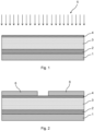
Figure 1 shows a cross-section of a semiconductor device prior to applying first masks, -
Figure 2 shows a cross-section of the semiconductor device with the first masks applied, -
Figure 3 shows a cross-section of the semiconductor device during a creation of a shield region, -
Figure 4 shows a cross-section of the semiconductor device with a second mask applied, -
Figure 5 shows a cross-section of the semiconductor device during a creation of well regions, -
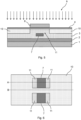
Figure 6 shows a top view of the semiconductor device, -
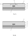
Figure 7a ,7b ,7c show a cross-section of the semiconductor device - the A cross-section as shown infigure 6 in different variants, -
Figure 8a ,8b ,8c show a cross-section of the semiconductor device - the B cross-section as shown infigure 6 in different variants, , -
Figure 8d shows a manufacturing process for a semiconductor device as shown infig. 8b and8c , -
Figure 9 shows a cross-section of the semiconductor device with a third mask applied -
Figure 10 shows a cross-section of the semiconductor device during a creation of source regions, -
Figure 11 shows a cross-section of a finished semiconductor device. - For a proper understanding of the disclosure, in the detailed description below corresponding elements or parts of the disclosure will be denoted with identical reference numerals in the drawings.
- A method of manufacturing a semiconductor device according to the invention, as briefly described, will comprise a following steps, which will be described in a greater detail hereinafter. The method comprising steps of :
- a) depositing of a first-conductivity-
type epitaxy layer 2 on top of a first-conductivity-type substrate 1, - b) depositing of a
scatter oxide layer 4 on top of the first-conductivity-type epitaxy layer 2, - c) creating a
first mask 6 on top of thescatter oxide layer 4, - d) creating a second-conductivity-
type shield region 7 in the first-conductivity-type epitaxy layer 2 byfirst implantation 14 of a first-conductivity-type dopant through thefirst mask 6, - e) removing the
first mask 6, - f) creating a
second mask 8 above the second-conductivity-type shield region 7, - g) creating
well regions 10 bysecond implantation 9 of second-conductivity-type dopant through thesecond mask 8, - h) creating the
third mask 12 which is wider than thesecond mask 8, - i) creating
source regions 15 bysecond implantation 13 of first-conductivity-type dopant through thethird mask 12. - First steps of manufacturing of a semiconductor device according to the invention are not shown in figures since those are the same steps as in the prior art methods. A first-conductivity-
type substrate 1 is used as a substrate, on which a first-conductivity-type epitaxy layer 2 is deposited - this layer serves as a drift layer for the semiconductor device. Next, on top of the first-conductivity-type epitaxy layer 2, ascatter oxide layer 4 is deposited to improve the subsequent implant processes. It should be noted that thescatter oxide layer 4 is only needed for the manufacturing process. A final structure will not have thescatter oxide layer 4. - It should be noted that throughout the whole description terms "first-conductivity-type" and "second-conductivity-type" will be used. Since the semiconductor device will have regions made as a semiconductor (typically silicon or germanium) doped with impurities for the purpose of modulating semiconductor's properties. Since mentioned impurities either provide electrons (impurities are donors) or holes (impurities are acceptors) those regions are often referred to as n-type or p-type regions. In this description it should be understood that in the case that the first-conductivity-type may mean p-type, the second-conductivity-type will be n-type. The invention will also work the other way around. The Applicant wishes not to focus on an exact types of regions but rather on a general idea behind this invention.
- In
fig. 1 an additional step of a surface-widefirst implantation 5 of first-conductivity type is shown, which is forming a second first-conductivity-type layer 3 within the first-conductivity-type epitaxy layer 2, which would alter theJFET region 11. Thefirst implantation 5 can be shallower or deeper than the subsequentsecond implantation 9 of second-conductivity-type dopant, which will form wellregions 10. In the following illustrations, a deeper variant is shown. - In
fig. 2 a final effect of a next step is shown which is a formation offirst masks 6. It should be noted that there is a gap between the first masks 6. It should be also noted that in a reality there might be a singlefirst mask 6 as shown infig. 6 , throughout the whole description, while referring to other figures, a plural form will be used. - In
fig. 3 afirst implantation 14 of second-conductivity-type dopant is shown. Through thefirst masks 6 an implant of a second-conductivity-type shield region 7 is performed, effectively creating a deep region of second conductivity type. For that, the doping concentration created by thefirst implantation 14 of second-conductivity-type dopant has to overcome that of the background doping of the first-conductivity-type epitaxy layer 2. If the surface-widefirst implantation 5 has been done the doping concentration of by thefirst implantation 14 of second-conductivity-type dopant has to overcome that of the surface-widefirst implantation 5. - A purpose of the second-conductivity-
type shield region 7 is that it will reduce an electrical field at a gate insulator interface at the completed transistor. A deeply implanted region below the gate, here the second-conductivity-type shield region 7, shields the gate from an elevated electric field that could potentially cause its deterioration or destruction. - In
fig. 4 a final effect of a next step is shown which is a formation of asecond mask 8. Thesecond mask 8 is created after the removal of thefirst mask 6 on thescatter oxide layer 4. Thesecond mask 8 is located above the previously implanted second-conductivity-type shield region 7 - In
fig. 5 asecond implantation 9 of second-conductivity-type dopant is shown. After this step thewell regions 10 will be formed. The second-conductivity type wellregions 10 are implanted in such a way that they are not as deep as the second-conductivity-type shield region 7. The region between thewell regions 10 is called theJFET region 11. Anything lower than the bottom of the second-conductivitytype well region 10 is no longer aJFET region 11. - In
fig. 6 a top view of the semiconductor device is shown after thesecond implantation 9 of second-conductivity-type dopant. Two cross-sections A and B are shown infig. 7a ,7b ,7c and8a ,7b ,7c respectively. To fully use the shielding potential of the second-conductivity-type shield region 7, it should not be left floating but should be electrically connected to the source potential. For this, the second-conductivity-type shield region 7 could be connected to thewell region 10 in the depth of the semiconductor. One end or both ends of second-conductivity-type shield region 7 may be connected to thewell region 10. It should be noted that different variants of theshield region 7 may be used - infig. 7a and7b theshield region 7 narrower than theJFET region 11 is present, wherein theshield region 7 top edge is on a similar depth as a lower edge of thewell region 10. Infig. 7a and7b theshield region 7 is located deeper than infig. 7a and7b - it should be noted that thewell region 10 must go deeper than previously so that thewell region 10 is able to connect to theshield region 7. Infig 7c and 8c theshield region 7 is as deep as infig. 7b and7c however it is now longer than theJFET region 11. Infig. 8d a manufacturing of the deeper part of thewell region 10, as presented infig. 8b and8c , is shown. Additional masks, namely fourth masks 19, are placed over thewell regions 10. In a desired place for a contact, in this example in the B cross-sections, athird implantation 20 of second-conductivity-type dopant is performed such that both wellregions 10 and theshield region 7 are connected. After this step thefourth masks 19 are removed. - In
fig. 9 a final effect of a next step is shown which is a formation of athird mask 12. It should be noted that preferably thethird mask 12 is created by adding more spacers to thesecond mask 8, effectively resulting in a mask wider than thesecond mask 8. - In
fig. 10 asecond implantation 13 of first-conductivity-type dopant is shown. This step results in a creation of thesource regions 15. - Subsequent manufacturing of gate oxides, terminal contacts at gate/drain/source, interlayer dielectrics, metallizations and passivations are done to complete the device, as typically is done during a standard manufacturing process. These steps are not a key feature of the device and are therefore not described in a greater detail since the person skilled in the art will know how to finish a product as described in this application.
- During the abovementioned process a half-finished semiconductor device is manufactured which comprises a first-conductivity-
type substrate 1, a first-conductivity-type epitaxy layer 2 comprising aJFET region 11 and a second-conductivity-type shield region 7, twowell regions 10 comprising twosource regions 15, and ascatter oxide layer 4. The first-conductivity-type substrate 1 is adjacent to the first-conductivity-type epitaxy layer 2. The twowell regions 10 are adjacent to the first-conductivity-type epitaxy layer 2. TheJFET region 11 is adjacent to the twowell regions 10. Thescatter oxide layer 4 is the outermost layer and is adjacent to the twosource regions 15, the twowell regions 10 and theJFET region 11. - The semiconductor device, as a finished product, comprising a first-conductivity-
type substrate 1, a first-conductivity-type epitaxy layer 2 comprising aJFET region 11 and a second-conductivity-type shield region 7, twowell regions 10 comprising twosource regions 15,gate oxide 17 comprising agate 16, adrain 18 adjacent to the first-conductivity-type substrate 1. The first-conductivity-type substrate 1 is adjacent to the first-conductivity-type epitaxy layer 2.The twowell regions 10 are adjacent to the first-conductivity-type epitaxy layer 2, TheJFET region 11 is located between the twowell regions 10. The source contact region is adjacent to the twosource regions 15. Thegate oxide 17 is adjacent to the twowell regions 10, the twosource regions 15, and theJFET region 11. - In another embodiment the second-conductivity-
type shield region 7 is narrower than theJFET region 11. - The second-conductivity-
type shield region 7 is located at a depth deeper than a lower edge of thewell regions 10 or at the same depth as the lower edge of the well regions (10), and at least part of the second-conductivity-type shield region 7 overlaps with theJFET region 11. - In yet another embodiment distance of the second-conductivity-
type shield region 7 to each of the twowell regions 10 is the same. - As mentioned herein before the first-conductivity-
type epitaxy layer 2 may comprise a second first-conductivity-type layer 3 such that atleast JFET region 11, and preferably the second-conductivity-type shield region 7, is located within the second first-conductivity-type layer 3, wherein the second first-conductivity-type layer 3 has a higher dopant concentration than the first-conductivity-type epitaxy layer 2. - The semiconductor device manufactured as described hereinbefore will have the second-conductivity-
type shield region 7 which comprising dopants of both types. However it should be noted that other manufacturing steps may be taken and such structure with both dopant types may not be present. Preferably the second-conductivity-type shield region 7 is doped to at least the same doping concentration as thewell region 10, even more preferably the second-conductivity-type shield region 7 is doped such that it has higher doping concentration than thewell region 10. - In another embodiment the second-conductivity-
type shield region 7 edges are rounded - sharp edges will result in high electric fields which should be avoided. - If the second-conductivity-
type shield region 7 is too small, there may not be a shielding effect (as the shielding reach is smaller); and if it is too large this may restrict current flow which may be beneficial in some kinds of protection elements such as an electric fuse. -
- 1
- first-conductivity-type substrate
- 2
- first-conductivity-type epitaxy layer
- 3
- second first-conductivity-type layer
- 4
- scatter oxide layer
- 5
- first implantation of first-conductivity-type dopant
- 6
- first mask
- 7
- second-conductivity-type shield region
- 8
- second mask
- 9
- second implantation of second-conductivity-type dopant
- 10
- well region
- 11
- JFET region
- 12
- third mask
- 13
- second implantation of first-conductivity-type dopant
- 14
- first implantation of second-conductivity-type dopant
- 15
- source region
- 16
- gate
- 17
- gate oxide
- 18
- drain
- 19
- fourth mask
- 20
- third implantation of second-conductivity-type dopant
Claims (13)
- A semiconductor device comprising:a first-conductivity-type substrate (1),a first-conductivity-type epitaxy layer (2) comprising a JFET region (11) and a second-conductivity-type shield region (7),two well regions (10) comprising two source regions (15),gate oxide (17) comprising a gate (16),a drain (18) adjacent to the first-conductivity-type substrate (1),wherein the first-conductivity-type substrate (1) is adjacent to the first-conductivity-type epitaxy layer (2),wherein the two well regions (10) are adjacent to the first-conductivity-type epitaxy layer (2),wherein the JFET region (11) is located between the two well regions (10),wherein the source contact region is adjacent to the two source regions (15),wherein the gate oxide (17) is adjacent to the two well regions (10), the two source regions (15), and the JFET region (11).
- The semiconductor device according to claim 1, wherein the second-conductivity-type shield region (7) is located at a depth deeper than a lower edge of the well regions (10) or at the same depth as the lower edge of the well regions (10), and at least part of the second-conductivity-type shield region (7) overlaps with the JFET region (11).
- The semiconductor device according to claim 1 or 2, wherein a distance of the second-conductivity-type shield region (7) to each of the two well regions (10) is the same.
- The semiconductor device according to anyone of the previous claims, wherein the first-conductivity-type epitaxy layer (2) comprising a second first-conductivity-type layer (3) such that at least JFET region (11), and preferably the second-conductivity-type shield region (7), is located within the second first-conductivity-type layer (3), wherein the second first-conductivity-type layer (3) has a higher dopant concentration than the first-conductivity-type epitaxy layer (2).
- The semiconductor device according to anyone of the previous claims, wherein the second-conductivity-type shield region (7) comprises dopants of both types.
- The semiconductor device according to anyone of the previous claims, wherein the second-conductivity-type shield region (7) is doped to the same doping concentration as the well region (10).
- The semiconductor device according to anyone of the claims 1-6, wherein the second-conductivity-type shield region (7) is doped such that it has higher doping concentration than the well region (10).
- The semiconductor device according to anyone of the previous claims, wherein the second-conductivity-type shield region (7) edges are rounded.
- The semiconductor device according to anyone of the previous claims, wherein at least one end of the second-conductivity-type shield region (7) is connected to the well region (10), preferably both ends of the second-conductivity-type shield region (7) are connected to the well region (10).
- A method of manufacturing a semiconductor device according to anyone of the claims 1-8, comprising steps of:a) depositing of a first-conductivity-type epitaxy layer (2) on top first-conductivity-type substrate (1),b) depositing of a scatter oxide layer (4) on top of the first-conductivity-type epitaxy layer (2),c) creating a first mask (6) on top of the scatter oxide layer (4),d) creating a second-conductivity-type shield region (7) in the first-conductivity-type epitaxy layer (2) by first implantation (5) of a second-conductivity-type dopant through the first mask (6),e) removing the first mask (6),f) creating a second mask (8) above the second-conductivity-type shield region (7),g) creating well regions (10) by second implantation (9) of second-conductivity-type dopant through the second mask (8),h) creating the third mask (12) which is wider than the second mask (8),i) creating source regions (15) by second implantation (13) of first-conductivity-type dopant through the third mask (15).
- The method according to claim 10, wherein, after step b), a second first-conductivity-type layer (3) is created by a first implantation (5) of first-conductivity-type dopant on the first-conductivity-type epitaxy layer (2).
- The method according to claim 10 or 11, wherein, during step h), the third mask (12) is created by adding spacers to the second mask (8).
- The method according to anyone of claims 10-12, wherein, after step g), a fourth mask (19) is placed over the well regions (10) and the third implantation (20) of second-conductivity-type dopant such that the connection between the well regions (10) and the second-conductivity-type shield region (7) is created.
Priority Applications (3)
| Application Number | Priority Date | Filing Date | Title |
|---|---|---|---|
| EP23201063.7A EP4531109A1 (en) | 2023-09-29 | 2023-09-29 | Semiconductor device and method of manufacturing semiconductor device |
| CN202411350652.8A CN119767737A (en) | 2023-09-29 | 2024-09-26 | Semiconductor device and method for manufacturing semiconductor device |
| US18/901,092 US20250113552A1 (en) | 2023-09-29 | 2024-09-30 | Semiconductor device and method of manufacturing semiconductor device |
Applications Claiming Priority (1)
| Application Number | Priority Date | Filing Date | Title |
|---|---|---|---|
| EP23201063.7A EP4531109A1 (en) | 2023-09-29 | 2023-09-29 | Semiconductor device and method of manufacturing semiconductor device |
Publications (1)
| Publication Number | Publication Date |
|---|---|
| EP4531109A1 true EP4531109A1 (en) | 2025-04-02 |
Family
ID=88241349
Family Applications (1)
| Application Number | Title | Priority Date | Filing Date |
|---|---|---|---|
| EP23201063.7A Pending EP4531109A1 (en) | 2023-09-29 | 2023-09-29 | Semiconductor device and method of manufacturing semiconductor device |
Country Status (3)
| Country | Link |
|---|---|
| US (1) | US20250113552A1 (en) |
| EP (1) | EP4531109A1 (en) |
| CN (1) | CN119767737A (en) |
Citations (8)
| Publication number | Priority date | Publication date | Assignee | Title |
|---|---|---|---|---|
| JP2011258635A (en) * | 2010-06-07 | 2011-12-22 | Mitsubishi Electric Corp | Semiconductor device |
| US20150053999A1 (en) * | 2013-08-23 | 2015-02-26 | Fuji Electric Co., Ltd. | Wide bandgap insulated gate semiconductor device |
| US9530844B2 (en) | 2012-12-28 | 2016-12-27 | Cree, Inc. | Transistor structures having reduced electrical field at the gate oxide and methods for making same |
| US9685550B2 (en) | 2014-12-26 | 2017-06-20 | Fairchild Semiconductor Corporation | Silicon carbide (SiC) device with improved gate dielectric shielding |
| CN107331707A (en) * | 2017-06-29 | 2017-11-07 | 电子科技大学 | VDMOS device with anti-single particle effect |
| JP6338134B2 (en) | 2012-03-30 | 2018-06-06 | 富士電機株式会社 | Silicon carbide vertical MOSFET and manufacturing method thereof |
| JP2020102596A (en) * | 2018-12-25 | 2020-07-02 | トヨタ自動車株式会社 | Semiconductor device |
| US20210242319A1 (en) * | 2020-01-31 | 2021-08-05 | Alpha And Omega Semiconductor (Cayman) Ltd. | Silicon carbide trench semiconductor device |
-
2023
- 2023-09-29 EP EP23201063.7A patent/EP4531109A1/en active Pending
-
2024
- 2024-09-26 CN CN202411350652.8A patent/CN119767737A/en active Pending
- 2024-09-30 US US18/901,092 patent/US20250113552A1/en active Pending
Patent Citations (9)
| Publication number | Priority date | Publication date | Assignee | Title |
|---|---|---|---|---|
| JP2011258635A (en) * | 2010-06-07 | 2011-12-22 | Mitsubishi Electric Corp | Semiconductor device |
| JP6338134B2 (en) | 2012-03-30 | 2018-06-06 | 富士電機株式会社 | Silicon carbide vertical MOSFET and manufacturing method thereof |
| US9530844B2 (en) | 2012-12-28 | 2016-12-27 | Cree, Inc. | Transistor structures having reduced electrical field at the gate oxide and methods for making same |
| US20150053999A1 (en) * | 2013-08-23 | 2015-02-26 | Fuji Electric Co., Ltd. | Wide bandgap insulated gate semiconductor device |
| US9093493B2 (en) | 2013-08-23 | 2015-07-28 | Fuji Electric Co., Ltd. | Wide bandgap insulated gate semiconductor device |
| US9685550B2 (en) | 2014-12-26 | 2017-06-20 | Fairchild Semiconductor Corporation | Silicon carbide (SiC) device with improved gate dielectric shielding |
| CN107331707A (en) * | 2017-06-29 | 2017-11-07 | 电子科技大学 | VDMOS device with anti-single particle effect |
| JP2020102596A (en) * | 2018-12-25 | 2020-07-02 | トヨタ自動車株式会社 | Semiconductor device |
| US20210242319A1 (en) * | 2020-01-31 | 2021-08-05 | Alpha And Omega Semiconductor (Cayman) Ltd. | Silicon carbide trench semiconductor device |
Also Published As
| Publication number | Publication date |
|---|---|
| CN119767737A (en) | 2025-04-04 |
| US20250113552A1 (en) | 2025-04-03 |
Similar Documents
| Publication | Publication Date | Title |
|---|---|---|
| US12057482B2 (en) | MOSFET with distributed doped P-shield zones under trenches | |
| US10553437B2 (en) | Semiconductor device and method for manufacturing such a semiconductor device | |
| US7960786B2 (en) | Breakdown voltages of ultra-high voltage devices by forming tunnels | |
| US20220130996A1 (en) | Gate trench power semiconductor devices having improved deep shield connection patterns | |
| US20020053695A1 (en) | Split buried layer for high voltage LDMOS transistor | |
| US10069006B2 (en) | Semiconductor device with vertical field floating rings and methods of fabrication thereof | |
| DE112013006308T5 (en) | Silicon carbide semiconductor device and method for its production | |
| US12279448B2 (en) | Trench bottom shielding methods and approaches for trenched semiconductor device structures | |
| US20200220009A1 (en) | Trench mosfet contacts | |
| US20040097019A1 (en) | Semiconductor component and method of manufacturing | |
| EP3806161B1 (en) | Silicon carbide device with an implantation tail compensation region | |
| EP3896744A1 (en) | Termination for trench field plate power mosfet | |
| US20220130997A1 (en) | Gate trench power semiconductor devices having improved deep shield connection patterns | |
| KR19990050418A (en) | Power Device with Double Field Plate Structure | |
| KR102359373B1 (en) | Method of fabricating a high voltage semiconductor device | |
| US20250133781A1 (en) | Semiconductor device and method of manufacturing semiconductor device | |
| US20250113552A1 (en) | Semiconductor device and method of manufacturing semiconductor device | |
| CN120091612A (en) | Semiconductor component and method for producing a semiconductor component | |
| CN120091577A (en) | Method for producing a semiconductor component and semiconductor component | |
| CN107871782A (en) | double-diffusion metal oxide semiconductor element and manufacturing method thereof | |
| JP5037103B2 (en) | Silicon carbide semiconductor device | |
| KR20220124345A (en) | Superjunction semiconductor device with differntial effective thickness and method for manufacturing same | |
| CN114520264A (en) | High voltage semiconductor device | |
| JP7555490B2 (en) | Vertical semiconductor device and its manufacturing method |
Legal Events
| Date | Code | Title | Description |
|---|---|---|---|
| PUAI | Public reference made under article 153(3) epc to a published international application that has entered the european phase |
Free format text: ORIGINAL CODE: 0009012 |
|
| STAA | Information on the status of an ep patent application or granted ep patent |
Free format text: STATUS: THE APPLICATION HAS BEEN PUBLISHED |
|
| AK | Designated contracting states |
Kind code of ref document: A1 Designated state(s): AL AT BE BG CH CY CZ DE DK EE ES FI FR GB GR HR HU IE IS IT LI LT LU LV MC ME MK MT NL NO PL PT RO RS SE SI SK SM TR |
|
| STAA | Information on the status of an ep patent application or granted ep patent |
Free format text: STATUS: REQUEST FOR EXAMINATION WAS MADE |
|
| 17P | Request for examination filed |
Effective date: 20251002 |