EP4529201A1 - Kamera mit bildsensor und elektronische vorrichtung mit kamera - Google Patents
Kamera mit bildsensor und elektronische vorrichtung mit kamera Download PDFInfo
- Publication number
- EP4529201A1 EP4529201A1 EP23812175.0A EP23812175A EP4529201A1 EP 4529201 A1 EP4529201 A1 EP 4529201A1 EP 23812175 A EP23812175 A EP 23812175A EP 4529201 A1 EP4529201 A1 EP 4529201A1
- Authority
- EP
- European Patent Office
- Prior art keywords
- circuit board
- image sensor
- flexible circuit
- camera module
- section
- Prior art date
- Legal status (The legal status is an assumption and is not a legal conclusion. Google has not performed a legal analysis and makes no representation as to the accuracy of the status listed.)
- Pending
Links
Images


Classifications
-
- H—ELECTRICITY
- H04—ELECTRIC COMMUNICATION TECHNIQUE
- H04N—PICTORIAL COMMUNICATION, e.g. TELEVISION
- H04N23/00—Cameras or camera modules comprising electronic image sensors; Control thereof
- H04N23/60—Control of cameras or camera modules
- H04N23/68—Control of cameras or camera modules for stable pick-up of the scene, e.g. compensating for camera body vibrations
- H04N23/682—Vibration or motion blur correction
- H04N23/685—Vibration or motion blur correction performed by mechanical compensation
- H04N23/687—Vibration or motion blur correction performed by mechanical compensation by shifting the lens or sensor position
-
- G—PHYSICS
- G03—PHOTOGRAPHY; CINEMATOGRAPHY; ANALOGOUS TECHNIQUES USING WAVES OTHER THAN OPTICAL WAVES; ELECTROGRAPHY; HOLOGRAPHY
- G03B—APPARATUS OR ARRANGEMENTS FOR TAKING PHOTOGRAPHS OR FOR PROJECTING OR VIEWING THEM; APPARATUS OR ARRANGEMENTS EMPLOYING ANALOGOUS TECHNIQUES USING WAVES OTHER THAN OPTICAL WAVES; ACCESSORIES THEREFOR
- G03B13/00—Viewfinders; Focusing aids for cameras; Means for focusing for cameras; Autofocus systems for cameras
- G03B13/32—Means for focusing
- G03B13/34—Power focusing
- G03B13/36—Autofocus systems
-
- G—PHYSICS
- G03—PHOTOGRAPHY; CINEMATOGRAPHY; ANALOGOUS TECHNIQUES USING WAVES OTHER THAN OPTICAL WAVES; ELECTROGRAPHY; HOLOGRAPHY
- G03B—APPARATUS OR ARRANGEMENTS FOR TAKING PHOTOGRAPHS OR FOR PROJECTING OR VIEWING THEM; APPARATUS OR ARRANGEMENTS EMPLOYING ANALOGOUS TECHNIQUES USING WAVES OTHER THAN OPTICAL WAVES; ACCESSORIES THEREFOR
- G03B3/00—Focusing arrangements of general interest for cameras, projectors or printers
- G03B3/10—Power-operated focusing
-
- G—PHYSICS
- G03—PHOTOGRAPHY; CINEMATOGRAPHY; ANALOGOUS TECHNIQUES USING WAVES OTHER THAN OPTICAL WAVES; ELECTROGRAPHY; HOLOGRAPHY
- G03B—APPARATUS OR ARRANGEMENTS FOR TAKING PHOTOGRAPHS OR FOR PROJECTING OR VIEWING THEM; APPARATUS OR ARRANGEMENTS EMPLOYING ANALOGOUS TECHNIQUES USING WAVES OTHER THAN OPTICAL WAVES; ACCESSORIES THEREFOR
- G03B30/00—Camera modules comprising integrated lens units and imaging units, specially adapted for being embedded in other devices, e.g. mobile phones or vehicles
-
- H—ELECTRICITY
- H04—ELECTRIC COMMUNICATION TECHNIQUE
- H04M—TELEPHONIC COMMUNICATION
- H04M1/00—Substation equipment, e.g. for use by subscribers
- H04M1/02—Constructional features of telephone sets
-
- H—ELECTRICITY
- H04—ELECTRIC COMMUNICATION TECHNIQUE
- H04N—PICTORIAL COMMUNICATION, e.g. TELEVISION
- H04N23/00—Cameras or camera modules comprising electronic image sensors; Control thereof
- H04N23/50—Constructional details
- H04N23/54—Mounting of pick-up tubes, electronic image sensors, deviation or focusing coils
-
- H—ELECTRICITY
- H04—ELECTRIC COMMUNICATION TECHNIQUE
- H04N—PICTORIAL COMMUNICATION, e.g. TELEVISION
- H04N23/00—Cameras or camera modules comprising electronic image sensors; Control thereof
- H04N23/50—Constructional details
- H04N23/55—Optical parts specially adapted for electronic image sensors; Mounting thereof
-
- H—ELECTRICITY
- H04—ELECTRIC COMMUNICATION TECHNIQUE
- H04N—PICTORIAL COMMUNICATION, e.g. TELEVISION
- H04N23/00—Cameras or camera modules comprising electronic image sensors; Control thereof
- H04N23/57—Mechanical or electrical details of cameras or camera modules specially adapted for being embedded in other devices
-
- H—ELECTRICITY
- H04—ELECTRIC COMMUNICATION TECHNIQUE
- H04N—PICTORIAL COMMUNICATION, e.g. TELEVISION
- H04N23/00—Cameras or camera modules comprising electronic image sensors; Control thereof
- H04N23/60—Control of cameras or camera modules
- H04N23/68—Control of cameras or camera modules for stable pick-up of the scene, e.g. compensating for camera body vibrations
-
- H—ELECTRICITY
- H05—ELECTRIC TECHNIQUES NOT OTHERWISE PROVIDED FOR
- H05K—PRINTED CIRCUITS; CASINGS OR CONSTRUCTIONAL DETAILS OF ELECTRIC APPARATUS; MANUFACTURE OF ASSEMBLAGES OF ELECTRICAL COMPONENTS
- H05K1/00—Printed circuits
- H05K1/18—Printed circuits structurally associated with non-printed electric components
- H05K1/181—Printed circuits structurally associated with non-printed electric components associated with surface mounted components
-
- H—ELECTRICITY
- H05—ELECTRIC TECHNIQUES NOT OTHERWISE PROVIDED FOR
- H05K—PRINTED CIRCUITS; CASINGS OR CONSTRUCTIONAL DETAILS OF ELECTRIC APPARATUS; MANUFACTURE OF ASSEMBLAGES OF ELECTRICAL COMPONENTS
- H05K1/00—Printed circuits
- H05K1/18—Printed circuits structurally associated with non-printed electric components
- H05K1/189—Printed circuits structurally associated with non-printed electric components characterised by the use of flexible or folded printed circuits
-
- G—PHYSICS
- G03—PHOTOGRAPHY; CINEMATOGRAPHY; ANALOGOUS TECHNIQUES USING WAVES OTHER THAN OPTICAL WAVES; ELECTROGRAPHY; HOLOGRAPHY
- G03B—APPARATUS OR ARRANGEMENTS FOR TAKING PHOTOGRAPHS OR FOR PROJECTING OR VIEWING THEM; APPARATUS OR ARRANGEMENTS EMPLOYING ANALOGOUS TECHNIQUES USING WAVES OTHER THAN OPTICAL WAVES; ACCESSORIES THEREFOR
- G03B2205/00—Adjustment of optical system relative to image or object surface other than for focusing
- G03B2205/0053—Driving means for the movement of one or more optical element
Definitions
- Various embodiments presented herein relate to a camera for capturing an image and an electronic apparatus including the camera.
- a camera applied to a mobile phone may be located on at least one of a front surface and a rear surface and may operate to provide a function of capturing photos and videos.
- the camera may include an actuator configured to at least partially move the optical system or an image sensor to acquire clear photos and videos.
- the image sensor may be connected to be powered or to communicate with other components within the electronic apparatus.
- a flexible printed circuit board may be used to electrically connect the image sensor to other components.
- the types of optical systems included in a camera include a direct-under type optical system in which light passing through the optical axis of a camera lens from a subject directly enters an image sensor without being refracted, and a refraction type optical system in which light passing through the optical axis of a lens from a subject is refracted in the process of passing through components of the optical system and enters an image sensor.
- the refraction type optical system may also be referred to as a folded type optical system.
- a camera actuator for optical image stabilization and auto-focusing in the form of moving a lens carrier containing an optical system including a camera lens, drives a lens relative to a fixed image sensor, so a circuit (e.g., a printed circuit board (PCB)) interconnecting the image sensor and other components does not need to move.
- a circuit e.g., a printed circuit board (PCB)
- a repulsive force of a circuit interconnecting an image sensor and other components serves as an obstacle to the movement of the image sensor when the image sensor moves in a driving direction (e.g., the x-axis, the y-axis, or the z-axis direction).
- a circuit connector is configured on a metal surface in the form of a leaf spring that is deformed in the moving direction of the image sensor may be used, or a flexible circuit board connected to the image sensor may be folded or deformed several times or may be increased in the length of a deformable area to be easily deformed in the moving direction.
- a flexible circuit board may be extracted from a position corresponding to the central axis of an image sensor (e.g., a direction corresponding to the optical axis direction of the optical system), and in order to reduce the repulsive force, the flexible circuit board may be branched into two or more portions and placed on the bottom surface of an optical component (e.g., a lens barrel or a prism).
- an optical component e.g., a lens barrel or a prism
- circuit connector configured on a metal surface in the form of a leaf spring when a circuit connector configured on a metal surface in the form of a leaf spring is used, the manufacturing cost of components of the camera increases.
- the circuit connector configured on the metal surface in the form of a leaf spring is applicable only in a limited structure.
- the manufacturing cost increases because a process for forming the folded structure is added.
- the actuator since the direction and magnitude of the repulsive force vary depending on the folded positions of the flexible circuit board, the actuator may be designed inefficiently to secure an extra driving force of the actuator, and current consumption of the actuator may increase.
- the length of the flexible circuit board is increased. Accordingly, noise of a signal transmitted through a conductive wire mounted on the flexible circuit board and resistance of the conductive wire may be increased.
- the structure of reducing the repulsive force by folding the flexible circuit board is easily applied to a structure of performing correction in the x-axis and y-axis to execute shift OIS, but it is difficult to form a structure for reducing the repulsive force that serves as an obstacle to z-axis driving for roll axis rotation correction and auto-focusing control.
- the branched flexible circuit board is placed on the central axis of a circuit board on which the image sensor is mounted in order to balance the repulsive force in opposite side directions of the branched area.
- the flexible circuit board is to be disposed on the bottom surface of an optical component (e.g., a lens barrel or a prism) to enable the optical system to function.
- the flexible circuit board cannot be disposed around the lens barrel facing a subject due to the position at which the flexible circuit board is extracted, the light-reception surface of the image sensor is inevitably disposed in substantially the same direction as the direction toward the subject.
- the structure of the device there is a limitation to form the structure of the device.
- a camera according to an embodiment or an electronic apparatus including the camera may include a circuit connector between an image sensor and a circuit in which a repulsive force is reduced by separating a flexible circuit board portions between areas in which conductive wires are mounted.
- a device in which a circuit connector between an image sensor and a circuit is configured by using a flexible circuit board that may be manufactured inexpensively and a repulsive force for movement of the image sensor generated due to the circuit connector may be reduced.
- a device in which components may be efficiently arranged without increasing the size of a camera module.
- a device capable of easily implementing roll rotation correction and auto-focusing functions (e.g., z-shift) in addition to 2-axis (x-axis, y-axis) optical image stabilization (OIS).
- a device in which a flexible circuit board is arranged in a form that at least partially surrounds the periphery of a position where an optical component is disposed in a camera module including a refraction type optical system while avoiding the position where the optical component is disposed so that the efficiency of component arrangement can be improved.
- the circuit connector 100 may include a flexible circuit board 120 including a section extracted from the circuit board 111 and extending in a first direction 151.
- the flexible circuit board 120 may include multiple conductive wires 121 configured to electrically connect the image sensor 110 or the circuit board 111 to other components.
- some portions between areas in which the multiple conductive wires 121 are disposed are separated.
- gaps may be provided in the flexible circuit board 120 to at least partially separate the portions between the areas in which the multiple conductive wires 121 are disposed.
- the gaps may include multiple slits 122 disposed side by side at least partially along the areas where the multiple conductive wires 121 are disposed.
- At least one of the position or the posture of the image sensor 110 may be controlled by an actuator.
- an actuator When the image sensor 110 is moved by the actuator, since a fixed portion 140 of the circuit connector 100 is fixed to the camera module or the electronic apparatus, a repulsive force against the movement of the image sensor 110 will act on the circuit board 111 by the connection structure between the fixed portion 140 and the circuit board 111.
- the flexible circuit board 120 by at least partially separating the portions between the areas in which the plurality of conductive wires 121 are disposed, it is possible to reduce the repulsive force.
- a structure in which the flexible circuit board is folded multiple times in a direction perpendicular to a direction in which the flexible circuit board moves may be applied.
- the length of the flexible circuit board is increased.
- the flexible circuit board 120 may include a section extending from one end of the section, which extends in the first direction 151, in a second direction 152 different from the first direction 151.
- the circuit connector 100 may include a rigid area or a stiffener 131 to maintain the shape of the bent area.
- the flexible circuit board 120 may further include a section bent at one end of the section extending in the first direction 151 and then curved to extend in the second direction 152.
- the stiffener 131 may be attached to an area including a bent area on the flexible circuit board 120.
- the flexible circuit board 120 illustrated in FIG. 1 is illustrated as including the section extending in the first direction 151, the section extending in the second direction 152, and the section extending in the third direction 153.
- the disclosure is not limited thereto. It should be noted that the embodiment illustrated in FIG. 1 is intended to describe a structure in which the flexible circuit board 120 configured such that multiple conductive wires are separated from each other extends in two or more directions, thereby reducing the repulsive force caused by the flexible circuit board 120 and facilitating the arrangement of other optical components.
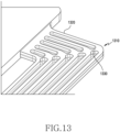
- a slit 122 may be formed between adjacent ones of the conductive wires 121 so that the conductive wires 121 can be separated from each other.
- Each conductive wire 121 may have a structure including three layers.
- polyimide PI may be disposed on both sides of each of conductors CU.
- the conductors CU may be disposed again on the polyimide PI on both sides, respectively, and areas in which respective conductive wires 121 are disposed may be configured in a structure in which each of the conductors is covered by the polyimide PI.
- the central portion of the area in which the flexible circuit board 120 including the conductive wires 121 is connected to the circuit board 111 configured to mount the image sensor 110 thereon does not need to be extracted from the central portion of one side of the circuit board 111, but may be extracted from an unrestricted position and may extend in a specific direction on the first plane.
- the first plane may be a light receiving surface of the image sensor 110 or a surface substantially parallel to the light receiving surface.
- the first plane may be a plane substantially perpendicular to the light receiving surface of the image sensor 110.
- the arrangement of the first plane is not limited to the above-described example.
- the shape in which the flexible circuit board 120 extends is not limited to a single straight line.
- the flexible circuit board 120 may have a shape of being extracted from the circuit board 111, extending in the first direction 151, and then extending in the second direction 152 different from the first direction 151.
- the flexible circuit board 120 may have a shape of extending in the z-axis direction, then extending in the x-axis direction, and extending in the y-axis direction from one end of the portion extending in the x-axis direction.
- the first direction 151 may be the -x-axis direction
- the second direction 152 may be the -y-axis direction
- the third direction may be the x-axis direction.
- the flexible circuit board 120 extending from the circuit board 111 may be attached to a fixed portion 140 including a rigid area at a fixed position in the camera module or an area reinforced by a stiffener.
- the flexible circuit board 120 one side of which is fixed may extend to be fixed to a camera module or an electronic apparatus including the camera module and may configure a connector 141.
- the flexible circuit board 120 may be bent in the state in which the conductive wires are joined together without a slit machined between adjacent ones of the conductive wires.
- a rigid stiffener may be attached to the flexible circuit board 120 to maintain the bent shape at the bent position.
- the connector 141 of the circuit connector 100 may be fixed to a camera module or an electronic apparatus including the camera module.
- FIG. 2 is a view for explaining a structure in which the flexible circuit board 120 is folded and bent.
- the description "the flexible circuit board 120 is bent" in this specification may refer to a structure obtained by folding the flexible circuit board 120, which causes the direction in which the flexible circuit board 120 extends to change.
- the folded point 210 of the flexible circuit board 120 at least some of the conductive wires 121 of the flexible circuit board 120 extending in a first direction 231 may be disposed in a first plane 221.
- the folded point 210 of the flexible circuit board 120 at least some of the conductive wires 121 of the flexible circuit board 120 extending in the second direction 232 may be disposed in a second plane 222 which is not parallel to the first plane 221.
- An area where the flexible circuit board 120 includes the folded point 210 may be referred to as a bent area.
- the flexible circuit board 120 illustrated in FIG. 2 has been described with reference to the shape thereof in a state in which no external force is applied thereto.
- the structure of the flexible circuit board 120 illustrated in FIG. 2 is merely an example for defining terms for describing various embodiments, and terms used in this specification are not limited to meaning that the disclosure should be physically completely identical to the shape illustrated in FIG. 2 .
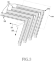
- FIG. 3 is a view for explaining a structure in which a direction in which a flexible circuit board 120 extends is curved.
- the description "the flexible circuit board 120 is curved" in this specification may mean a structure in which the direction in which the conductive wires 121 disposed on the flexible circuit board 120 are disposed to extend changes with reference to a curved point 310. As the direction in which the conductive wires 121 are disposed to extend changes, the direction in which the flexible circuit board 120 extends may also change.
- the conductive wires 121 included in the flexible circuit board 120 extending in a first direction 331 with reference to the curved point 310 and the conductive wires 121 included in the flexible circuit board 120 extending in a second direction 332 may be disposed on one plane 320.
- An area including the curved point 310 in which the flexible circuit board 120 is curved may be referred to as a curved area.
- the flexible circuit board 120 illustrated in FIG. 3 has been described with reference to the shape thereof in a state in which no external force is applied thereto.
- the structure of the flexible circuit board 120 illustrated in FIG. 3 is merely an example for defining terms for describing various embodiments, and terms used in this specification are not limited to meaning that the disclosure should be physically completely identical to the shape illustrated in FIG. 3 .
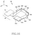
- FIG. 4 is an exploded view illustrating the configuration of a camera module 400 according to an embodiment.
- the camera module 400 may include an upper shield can 411 and a lower shield can 413.
- the components of the camera module 400 may be accommodated in a space defined between the upper shield can 411 and the lower shield can 413.
- the image sensor 110 of the camera module 400 may be connected to an external circuit of the camera module 400 via the circuit connector 100.
- the image sensor 110 may be disposed on a carrier (e.g., at least one of an OIS carrier 451 or an AF carrier 441).
- the OIS carrier 451 may be driven by an attractive or repulsive force (or Lorentz force) generated between OIS coils 453 and 454 and OIS magnets 455 and 456.
- the AF carrier 441 may be driven by an attractive force or repulsive force (or Lorentz force) generated between an AF coil 443 and an AF magnet (not illustrated).
- an attractive force or repulsive force or Lorentz force
- the image sensor 110 may be fixed to the carrier.
- the image sensor 110 fixed to the carrier may move as the carrier is driven.
- the camera module 400 may further include a housing 420 configured to arrange other components included in the camera module 400 at appropriate positions within the camera module 400.
- the camera module 400 may include an optical system including a lens 431 and a prism 433.
- the camera module 400 according to an embodiment may include a refraction type optical system in which a light path extending from a subject to the image sensor 110 via the lens 431 and the prism 433 is refracted one or more times.
- the camera module 400 may include an AF actuator configured to provide an auto-focusing function.
- the AF actuator may include an AF carrier 441, an AF coil 443, an AF magnet (not illustrated), and AF balls 447.
- the AF magnet (not illustrated) may be disposed on one surface of the AF carrier 441 facing the AF coil 443.
- the AF carrier 441 may be driven by an attractive or repulsive force between an AF magnet (not illustrated) and the AF coil 443.
- the moving path of the AF carrier 441 may be guided by a guide groove provided to allow the AF balls 447 to roll therein (e.g., a rail provided in the AF carrier 441).
- the image sensor 110 disposed on the AF carrier 441 moves so that a focus control function can be executed.
- the camera module 400 may include an OIS actuator configured to provide an optical image stabilization function.
- the OIS actuator may include an OIS carrier 451, y-axis OIS coils 453, y-axis OIS magnets 455, an x-axis OIS coil 454, an x-axis OIS magnet 456, and an OIS balls 457.
- the y-axis OIS magnets 455 may be disposed on one surface of the OIS carrier 451 facing the y-axis OIS coils 453.
- the x-axis OIS magnet 456 may be disposed on one surface of the OIS carrier 451 facing the x-axis OIS coil 454.
- the OIS carrier 451 may be driven by an attractive or repulsive force between the y-axis OIS coils 453 and the y-axis OIS magnets 455 and/or an attractive or repulsive force between the x-axis OIS coil 454 and the x-axis OIS magnet 456.
- the movement of the OIS carrier 451 may be guided by a guide groove provided to allow the OIS balls 457 to roll therein (e.g., a rail provided in the OIS carrier 451).
- the image sensor 110 disposed on the OIS carrier 451 moves so that an optical image stabilization function can be executed.
- the camera module 400 may further include a z-axis stopper 460 and a circuit board 470.
- the z-axis stopper 460 may limit the movement range of the OIS carrier 451 and/or the AF carrier 441 in the z-axis direction.
- the circuit board 470 may be connected to at least one of the AF coil 443, the y-axis OIS coil 453, or the x-axis OIS coil 454.
- the circuit board 470 may include a flexible printed circuit board (FPCB).
- Components of the camera module 400 illustrated in FIG. 4 are for explaining an embodiment, and the camera module 400 according to an embodiment may further include other components or some of the components may be omitted. Alternatively, the camera module 400 may include multiple components illustrated in FIG. 4 , as a single component. For example, although two y-axis OIS coils 453 and y-axis OIS magnets 455 are illustrated in FIG. 4 , the camera module according to an embodiment may include a y-axis OIS actuator that may be configured with one y-axis OIS coil and one y-axis OIS magnet. According to an embodiment, the magnets and coils of the OIS actuator may be arranged in a solenoid method other than a Lorentz method. As another example, FIG.
- FIG. 4 illustrates the camera module 400 in which the OIS carrier 451 and the AF carrier 441 are guided using the OIS balls 457 and the AF balls 447, but at least one of the OIS carrier 451 or the AF carrier 441 may be guided by using a wire.
- FIG. 5 is a view illustrating a structure of a circuit connector 100 configured to interconnect an image sensor 110 according to an embodiment and components other than the image sensor.
- a flexible circuit board 120 may include a bent section 510 bent to extend in the y-axis direction from a position where the flexible circuit board 120 is extracted from a circuit board 111 on which the image sensor 110 is disposed.
- a rigid area or a stiffener may be disposed in the bent section 510 to maintain the shape of the flexible circuit board 120.
- the flexible circuit board 120 may include a section extending in the y-axis direction from the bent section 510.
- the flexible circuit board 120 may be curved in the bent section 510 and may then extend in the z-axis direction. Referring to FIG.
- the surface on which the flexible circuit board 120 is disposed may not be parallel to the plane where the light-receiving surface of the image sensor 110 is disposed (e.g., the x-z plane).
- the flexible circuit board 120 may be bent to extend in the -x-axis direction from one end of the portion extending in the z-axis direction.
- the flexible circuit board 120 may further include a section extending in the -x-axis direction from the bent section 511.
- a rigid area or a stiffener configured to maintain the shape of the flexible circuit board 120 may be disposed in the section 511 in which the flexible circuit board 120 bent at one end of the portion extending in the z-axis direction is bent.
- the flexible circuit board 120 may be bent to extend in the -z-axis direction from one end of the portion extending in the -x-axis direction.
- the flexible circuit board 120 may further include a section extending in the -z-axis direction from the bent section 512.
- One end of the portion of the flexible circuit board 120 extending in the -z-axis direction may be connected to a fixed portion 140.
- the fixed portion 140 may include or be connected to a connector for connecting to another circuit.
- a rigid area or a stiffener may be disposed in the bent section 512 to maintain the shape of the flexible circuit board 120.
- an optical system (not illustrated) included in a camera module (not illustrated) may be disposed in the space 520, which is at least partially surrounded by the flexible circuit board 120.
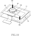
- FIG. 6 is a view illustrating an example of a state in which the camera module 400 illustrated in FIG. 5 is mounted in an electronic apparatus 600 according to an embodiment.
- the camera module 400 may be disposed such that a lens 431 faces the outside of the electronic apparatus 600.
- the electronic apparatus 600 may further include other openings 610 in addition to the opening through which the lens 431 of the camera module 400 is exposed.
- the electronic apparatus 600 may further include other components disposed at positions within the electronic apparatus 600 corresponding to positions where the other openings 610 are formed.
- the electronic apparatus 600 may further include at least one of a camera, a proximity sensor, or a flash.
- FIG. 6 illustrates an example in which the camera module 400 is disposed in the electronic apparatus 600, and the position of the camera module 400 in the electronic apparatus 600 is not limited to the example illustrated in FIG. 6 .
- the camera module 400 may be an under-display camera (UDC) disposed on the rear surface of a display of the electronic apparatus 600.
- UDC under-display camera
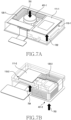
- FIGS. 7A and 7B are views illustrating respectively a direction in which light enters a camera module from a subject through a lens and a direction in which an image sensor receives light in a camera module according to various embodiments.
- a circuit board 111-1 on which an image sensor 110-1 according to an embodiment is mounted may be disposed on a side the lens 431-1 faces within the camera module.
- a flexible circuit board 120-1 may be extracted and extend from the circuit board 111-1 on which the image sensor 110-1 is mounted and may be disposed in a form at least partially surrounding a periphery of optical components (e.g., a lens barrel in which the lens 431-1 is housed in an inner space, a prism, or a reflective member including a reflector that reflects light).
- a first direction 701 in which light is incident on the lens 431-1 from a subject and a second direction 702 in which light is incident on the image sensor 110-1 may be substantially opposite to each other.
- the processor 1420 may execute, for example, software (e.g., a program 1440) to control at least one other component (e.g., a hardware or software component) of the electronic device 1401 coupled with the processor 1420, and may perform various data processing or computation. According to an embodiment, as at least part of the data processing or computation, the processor 1420 may store a command or data received from another component (e.g., the sensor module 1476 or the communication module 1490) in volatile memory 1432, process the command or the data stored in the volatile memory 1432, and store resulting data in non-volatile memory 1434.
- software e.g., a program 1440
- the processor 1420 may store a command or data received from another component (e.g., the sensor module 1476 or the communication module 1490) in volatile memory 1432, process the command or the data stored in the volatile memory 1432, and store resulting data in non-volatile memory 1434.
- the artificial neural network may be a deep neural network (DNN), a convolutional neural network (CNN), a recurrent neural network (RNN), a restricted boltzmann machine (RBM), a deep belief network (DBN), a bidirectional recurrent deep neural network (BRDNN), deep Q-network or a combination of two or more thereof but is not limited thereto.
- the artificial intelligence model may, additionally or alternatively, include a software structure other than the hardware structure.
- FIG. 19 is a view illustrating an example of a camera module in which a circuit connector according to an embodiment does not include slits.
- FIG. 20 is a view illustrating an example of a camera module in which a circuit connector according to an embodiment does not include slits.
- FIG. 20 illustrates a camera module including a flexible circuit board 120 which is not provided with slits, instead of the flexible circuit board 120-2 illustrated in (b) of FIG. 7 .
- the camera module may include the rhomboid prism 1433 configured to allow the light, which enters in a first direction 2001 through the lens 431, to be incident to the image sensor mounted on the circuit board in a second direction 2002 substantially parallel to the first direction 2001.
- FIG. 21 is a view illustrating directions in which a circuit connector may be deformed to allow movement of an image sensor as an optical image stabilization function or an auto-focusing function is executed according to an embodiment.
- the position of the image sensor 110 may be shifted because the flexible circuit board is made of a flexible material.
- the electronic device may drive the actuator included in the camera module such that the image sensor moves in at least one of the x-axis direction or the y-axis direction or changes the posture thereof to execute optical image stabilization.
- the circuit connector 100 of the camera module may include at least one operating section, of which the shape is deformable according to the movement of the image sensor 110.
- FIG. 8 illustrates an embodiment in which the circuit connector 100 includes a first operating section 711 extending from the image sensor 110, a second operating section 712 extending from the first operating section 711, and a third operating section 713 connected to a fixed portion 140 from the second operating section 712.
- the image sensor 110 may be moved by driving the actuator.
- the movement of the image sensor 110 in the x-axis direction 720 may be allowed while the second section 712 is deformed.
- the movement of the image sensor 110 in the y-axis direction 730 may be allowed while the third section 713 is deformed.
- the image sensor 110 may perform roll rotation about the z-axis to execute optical image stabilization.
- the roll rotation 740 of the image sensor 110 may be allowed while the first section 711 and the third section 713 are deformed.
- the flexible circuit board including the first section 711 and the third section 713 may be deformed while shifting and rotating on the x-y plane.
- the image sensor may move in the z-axis direction.
- the image sensor 110 moves in the z-axis direction 750 with reference to the fixed portion 140, the movement of the image sensor 110 in the z-axis direction 750 may be allowed while the first section 711 is deformed.
- the operating direction of the flexible circuit board included in the circuit connector 100 may vary depending on the extension direction and the bent or curved position of the flexible circuit board according to various embodiments.
- a concept in which at least one of the position or the posture of the image sensor is changed while the flexible circuit board is deformed in the operating direction and a low repulsive force is generated may be equally applicable.
- a section that is deformable as the image sensor is moved in the circuit connector 100 may be referred to as an operating section or an operating portion.
- a section which is not deformed and maintains a fixed shape even when the image sensor 110 is moved in the circuit connector 100 may be referred to as a fixed section or a fixed portion.
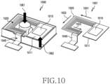
- FIG. 22 is a view illustrating a circuit connector 100 in which an area 2210 that is curved without slits is included in operating sections 711, 712, and 713 of a flexible circuit board, and a camera module 400 including the circuit connector 100 according to an embodiment.
- the circuit connector 100 of the camera module 400 may include a flexible circuit board 2220 in which no slits are present.
- the curved area 2210 may be included in the operating sections 711, 712, and 713 of the flexible circuit board 2220.
- the curved area 2210 may be provided to shift the position of the first operating section 711 so that one end of the first operating section 711 is connected to one end of the second operating section 712.
- the camera module 400 may further include a rhomboid prism 1733.
- FIG. 23 illustrates an example, in which a flexible circuit board is disposed on substantially the same plane as an image sensor, a circuit connector includes a bent area in an operating section, and the circuit connector is mounted in a camera module including a rhomboid prism, in an embodiment.
- the camera module 400 may include a rhomboid prism 1733, which is arranged such that light entering in a first direction 2361 through the lens 431 is incident to the image sensor 110 in a second direction 2362 substantially parallel to the first direction 2361.
- FIG. 24 illustrates a camera module 400, in which the direction in which light enters and the direction in which light is received by a sensor are substantially the same, in an embodiment.
- the camera module 400 may include a rhomboid prism 1733, which is arranged such that light entering in the first direction 2361 through the lens 431 is incident to the image sensor 110 in the second direction 2362 substantially parallel to the first direction 2361.
- the camera module 400 may include a flexible printed circuit board extends in the third direction 2451 without a slit from the substrate 111 on which the image sensor 110 is mounted, and extends in the fourth direction 2452 from one end extending in the third direction 2451.
- the flexible printed circuit board extending in the fourth direction 2452 may be connected to the fixed portion 2440.
- FIG. 25 is a configuration view illustrating an optical path in an optical system of a camera module (e.g., the camera module 400 in FIG. 4 or FIG. 17 ) according to an embodiment.
- FIG. 25 illustrates an example of an optical system including a rhomboid prism.
- an optical system included in a camera module may provide a first light path by refracting or reflecting light at least twice.
- a first light path may be indicated by a dotted line, and the light traveling along the first light path may follow the path indicated by "IL”, "RL1", “RL2”, “RL3”, and "RL4" in FIG. 25 .
- the first light path may be a light path that passes through the center of a lens included in an optical system and is substantially perpendicularly incident to the image sensor.
- the first light path may be provided by at least one reflective member included in the optical system and at least one lens that may be additionally provided to the at least one reflective member according to an embodiment.
- the optical system may include one reflective member 2513.
- the reflective member 2513 may include, for example, a trapezoidal prism or mirror structure.
- the reflective member 2513 may include, for example, a first reflective surface 2513a, a second reflective surface 2513b, a third reflective surface 2513c, and a fourth reflective surface 2513d.
- a first reflective surface 2513a, a second reflective surface 2513b, a third reflective surface 2513c, and a fourth reflective surface 2513d In the embodiment illustrated in FIG.
- the first reflective surface 2513a and the fourth reflective surface 2513d may be parallel to each other, and the second reflective surface 2513b and the third reflective surface 2513c may be parallel to each other.
- the reflective member 2513 may include a parallelogram prism or mirror structure.
- the optical system in the embodiment of the disclosure is not limited thereto.
- the first reflective surface 2413a and the fourth reflective surface 2513d may form an equilateral trapezoid having the second reflective surface 2513b or the third reflective surface 2513c as a base and having two equal interior angles (base angles).
- the reflective member 2513 included in the optical system of the camera module may include a one-body trapezoidal prism or mirror structure.
- the reflective member 2513 having a trapezoidal prism or mirror structure may be provided by combining and/or coupling a plurality of prism or mirror pieces.
- the optical system of the camera module may include a plurality of reflective members.
- the optical system may provide the first light path by including at least two reflective members to refract or reflect light at least twice.
- at least one lens system may be further included among the plurality of reflective members.
- the optical system may further include an infrared ray blocking filter (not illustrated).
- the optical system of the camera module may further include a lens system (e.g., the lens system 2531 including lenses 2531a and 2531b) configured to guide or focus light IL incident from the outside to at least one reflective member 2513.
- the first lens e.g., the first lens 2531a
- the optical system may have a refractive power.
- a camera including an optical system including the lens group 2531 may be referred to as a "lens lead-type camera".
- the lens group 2531 may further include an additional lens 2531b to focus or align light incident from the outside.
- the camera module 400 may include a dove-type prism having a trapezoidal shape instead of the rhomboid-type prism having a parallelogram shape illustrated in FIG. 25 .
- a trapezoidal prism or mirror structure or a parallelogram prism or mirror structure
- a refractive optical system including the same may be designed such that only the light that is refracted or reflected by each of the first reflective surface 2513a, the second reflective surface 2513b, the third reflective surface 2513c, and the fourth reflective surface 2513d, respectively, that is, such that only light refracted or reflected 4 times is incident to the image sensor.
- FIG. 25 a trapezoidal prism or mirror structure (or a parallelogram prism or mirror structure) and a refractive optical system including the same may be designed such that only the light that is refracted or reflected by each of the first reflective surface 2513a, the second reflective surface 2513b, the third reflective surface 2513c, and the fourth reflective surface 2513d, respectively, that is, such
- the light refracted or reflected by the reflective member 2513 may enter the image sensor 110 through a second optical path different from the first optical path.
- the second light path may be the path indicated by a one-dotted chain line.
- the light traveling along the second light path may follow the path indicated by "IL", "RL1", and "RL2"' in FIG. 25 .
- a trapezoidal prism or mirror structure or a parallelogram prism or mirror structure
- a refractive optical system including the same
- light refracted or reflected by the first reflective surface 2513a and the second reflective surface 2513b that is, light refracted or reflected twice is capable of being incident to the image sensor 110.
- An image obtained by such light may be output hazy due to occurrence of flare.
- the prism included in the camera module 400 may be the prism 433 having the shape illustrated in FIG. 4 .
- the prism included in the camera module 400 may be the prism 1733 having the shape illustrated in FIG. 17 .
- the components included in the embodiments presented in the disclosure may be used in combination with each other.
- the rhomboid-type or dove-type (parallelogram or trapezoidal) prism 1733 illustrated in FIG. 17 to 20 and 22 to 25 may be included in a camera module 400 including a flexible circuit board having the slits presented in FIG. 1 to 13 .
- a camera module may include a first circuit board (e.g., the circuit board 111 of FIG. 5 ) electrically connected to an image sensor (e.g., the image sensor 110 of FIG. 1 , the image sensor 110 of FIG. 4 , the image sensor 110 of FIG. 5 , the image sensors 110-1 and 110-2 of FIG. 7 , the image sensor 110 of FIG. 8 , the image sensor 1010 of FIG. 4 , the image sensor 1110 of FIG. 11 , or the image sensor 1210 of FIG. 12 ) or a circuit board including the image sensor (e.g., the image sensor 110 of FIG. 1 , the image sensor 110 of FIG.
- the image sensor 110 of FIG. 5 the image sensors 110-1 and 110-2 of FIG. 7 , the image sensor 110 of FIG. 8 , the image sensor 1010 of FIG. 4 , the image sensor 1110 of FIG. 11 , or the image sensor 1210 of FIG. 12
- an actuator configured to control at least one of the position or the posture of the first circuit board within the camera module (e.g., the camera module 400 of FIG. 4 or the camera module 1480 of FIG. 14 ), a flexible circuit board (e.g., the flexible circuit board 120 of FIG. 1 , the flexible circuit board 120 of FIG. 5 , the flexible circuit boards 120-1 and 120-2 of FIG. 7 , the flexible circuit board 1020 of FIG. 10 , the flexible circuit board 1120 of FIG.
- a flexible circuit board e.g., the flexible circuit board 120 of FIG. 1 , the flexible circuit board 120 of FIG. 5 , the flexible circuit boards 120-1 and 120-2 of FIG. 7 , the flexible circuit board 1020 of FIG. 10 , the flexible circuit board 1120 of FIG
- the flexible circuit board may include a first section (e.g., the first operating section 711 of FIG. 8 ) extracted or extending in a first direction from the first circuit board.
- the flexible circuit board may include a second section (e.g., the second operating section 712 in FIG.
- the flexible circuit board may be deformed as the actuator is driven.
- the flexible circuit board (e.g., the flexible circuit board 120 of FIG. 1 , the flexible circuit board 120 of FIG. 5 , the flexible circuit boards 120-1 and 120-2 of FIG. 7 , the flexible circuit board 1020 of FIG. 10 , the flexible circuit board 1120 of 11, or the flexible circuit board 1220 of FIG. 12 ) according to an embodiment may include, between the first section and the second section, a curved section in which the direction in which the flexible circuit board extends is changed. A smaller number of slits than the first section or no slits may be formed in the curved section.
- a camera module (e.g., the camera module 400 of FIG. 4 or the camera 1480 of FIG. 14 ) according to an embodiment may further include an optical system (e.g., the lens 431 of FIG. 4 , the prism 433 of FIG. 4 , the lens barrels 431-1 and 431-2 of FIG. 7 , or the lens 1231 of FIG. 12 ) configured to guide light incident from a subject to the image sensor (e.g., the image sensor 110 of FIG. 1 , the image sensor 110 of FIG. 4 , the image sensor 110 of FIG. 5 , the image sensors 110-1 and 110-2 of FIG. 7 , the image sensor 110 of FIG. 8 , the image sensor 1010 of FIG. 4 , the image sensor 1110 of FIG.
- an optical system e.g., the lens 431 of FIG. 4 , the prism 433 of FIG. 4 , the lens barrels 431-1 and 431-2 of FIG. 7 , or the lens 1231 of FIG. 12
- the image sensor e.g., the image
- the flexible circuit board is extracted at a position deviating from a central axis corresponding to an optical axis (e.g., the central axis 113 in FIG. 1 ) of the optical system on the at least one side surface of the first circuit board.
- an optical axis e.g., the central axis 113 in FIG. 1
- the camera module (e.g., the camera module 400 of FIG. 4 or the camera module 1480 of FIG. 14 ) according to an embodiment may include a housing (e.g., the housing 420 of FIG. 4 ) accommodating the first circuit board and the optical system.
- the flexible circuit board may be disposed along at least one surface of the housing around the optical system.
- the optical system may include a refraction type optical system in which an optical path through which light incident from the subject reaches the image sensor (e.g., the image sensor 110 of FIG. 1 , the image sensor 110 of FIG. 4 , the image sensor 110 of FIG. 5 , the image sensors 110-1 and 110-2 of FIG. 7 , the image sensor 110 of FIG. 8 , the image sensor 1010 of FIG. 4 , the image sensor 1110 of FIG. 11 , or the image sensor 1210 of FIG. 12 ) is refracted at least twice.
- the image sensor e.g., the image sensor 110 of FIG. 1 , the image sensor 110 of FIG. 4 , the image sensor 110 of FIG. 5 , the image sensors 110-1 and 110-2 of FIG. 7 , the image sensor 110 of FIG. 8 , the image sensor 1010 of FIG. 4 , the image sensor 1110 of FIG. 11 , or the image sensor 1210 of FIG. 12
- the image sensor e.g., the image sensor 110 of FIG. 1 , the image sensor 110 of FIG. 4 , the image sensor 110 of FIG. 5 , the image sensors 110-1 and 110-2 of FIG. 7 , the image sensor 110 of FIG. 8 , the image sensor 1010 of FIG. 4 , the image sensor 1110 of FIG. 11 , or the image sensor 1210 of FIG. 12
- a light detecting surface is oriented in an opposite direction to a direction in which light is incident from the subject to the optical system.
- the image sensor e.g., the image sensor 110 of FIG. 1 , the image sensor 110 of FIG. 4 , the image sensor 110 of FIG. 5 , the image sensors 110-1 and 110-2 of FIG. 7 , the image sensor 110 of FIG. 8 , the image sensor 1010 of FIG. 4 , the image sensor 1110 of FIG. 11 , or the image sensor 1210 of FIG. 12
- a light detecting surface is oriented in the same direction as the direction in which light is incident from the subject to the optical system.
- the flexible circuit board may further include a third section (e.g., the third operating section 713 of FIG. 3 ) extending in a third direction different from the second direction.
- a third section e.g., the third operating section 713 of FIG. 3
- the flexible circuit board may be configured such that the second section is deformed when the first circuit board moves in the first direction by the operation of the actuator.
- the flexible circuit board may be configured such that the third section is deformed when the first circuit board moves in the second direction by the operation of the actuator.
- the flexible circuit board may be configured such that the first section and the third section are deformed when the first circuit board rotates by the operation of the actuator.
- the actuator may include an auto-focusing actuator configured to provide an auto-focusing function.
- the flexible circuit board may be configured such that the first section is deformed as the auto-focusing actuator is driven.
- the flexible circuit board may include a folded and bent section between the first section and the second section where the flexible circuit board is folded, and a stiffener may be attached to the bent section.
- a camera module may include a first circuit board electrically connected to an image sensor (e.g., the image sensor 110 of FIG. 1 , the image sensor 110 of FIG. 4 , the image sensor 110 of FIG. 5 , the image sensors 110-1 and 110-2 of FIG. 7 , the image sensor 110 of FIG. 8 , the image sensor 1010 of FIG. 4 , the image sensor 1110 of FIG. 11 , or the image sensor 1210 of FIG. 12 ) or a circuit board including the image sensor (e.g., the image sensor 110 of FIG. 1 , the image sensor 110 of FIG. 4 , the image sensor 110 of FIG.
- the camera module 400 of FIG. 4 or the camera module 1480 of FIG. 14 e.g., the camera module 400 of FIG. 4 or the camera module 1480 of FIG. 14
- the flexible circuit board may include a first section extracted from a position deviated to one side from a central axis of the first circuit board and extending in a first direction, and a second section extending from one end of the first section in a second direction different from the first direction.
- the optical system may include a refraction type optical system in which an optical path through which light incident from the subject reaches the image sensor (e.g., the image sensor 110 of FIG. 1 , the image sensor 110 of FIG. 4 , the image sensor 110 of FIG. 5 , the image sensors 110-1 and 110-2 of FIG. 7 , the image sensor 110 of FIG. 8 , the image sensor 1010 of FIG. 4 , the image sensor 1110 of FIG. 11 , or the image sensor 1210 of FIG. 12 ) is refracted at least twice.
- the image sensor e.g., the image sensor 110 of FIG. 1 , the image sensor 110 of FIG. 4 , the image sensor 110 of FIG. 5 , the image sensors 110-1 and 110-2 of FIG. 7 , the image sensor 110 of FIG. 8 , the image sensor 1010 of FIG. 4 , the image sensor 1110 of FIG. 11 , or the image sensor 1210 of FIG. 12
- the image sensor e.g., the image sensor 110 of FIG. 1 , the image sensor 110 of FIG. 4 , the image sensor 110 of FIG. 5 , the image sensors 110-1 and 110-2 of FIG. 7 , the image sensor 110 of FIG. 8 , the image sensor 1010 of FIG. 4 , the image sensor 1110 of FIG. 11 , or the image sensor 1210 of FIG. 12
- a light detecting surface is oriented in an opposite direction to a direction in which light is incident from the subject to the optical system.
- the image sensor e.g., the image sensor 110 of FIG. 1 , the image sensor 110 of FIG. 4 , the image sensor 110 of FIG. 5 , the image sensors 110-1 and 110-2 of FIG. 7 , the image sensor 110 of FIG. 8 , the image sensor 1010 of FIG. 4 , the image sensor 1110 of FIG. 11 , or the image sensor 1210 of FIG. 12
- a light detecting surface is oriented in the same direction as the direction in which light is incident from the subject to the optical system.
- An electronic apparatus may include a camera module, a circuit board electrically connected to an image sensor (e.g., the image sensor 110 of FIG. 1 , the image sensor 110 of FIG. 4 , the image sensor 110 of FIG. 5 , the image sensors 110-1 and 110-2 of FIG. 7 , the image sensor 110 of FIG. 8 , the image sensor 1010 of FIG. 4 , the image sensor 1110 of FIG. 11 , or the image sensor 1210 of FIG. 12 ) or a circuit board including the image sensor (e.g., the image sensor 110 of FIG. 1 , the image sensor 110 of FIG. 4 , the image sensor 110 of FIG.
- the flexible circuit board (e.g., the flexible circuit board 120 of FIG. 1 , the flexible circuit board 120 of FIG. 5 , the flexible circuit boards 120-1 and 120-2 of FIG. 7 , the flexible circuit board 1020 of FIG. 10 , the flexible circuit board 1120 of FIG. 11 , or the flexible circuit board 1220 of FIG. 12 ) may include multiple conductive wires.
- the multiple slits may be disposed in parallel to the conductive wires.
- the flexible circuit board (e.g., the flexible circuit board 120 of FIG. 1 , the flexible circuit board 120 of FIG. 5 , the flexible circuit boards 120-1 and 120-2 of FIG. 7 , the flexible circuit board 1020 of FIG. 10 , the flexible circuit board 1120 of FIG. 11 , or the flexible circuit board 1220 of FIG. 12 ) may include a curved section in which a direction in which the flexible circuit board (e.g., the flexible circuit board 120 of FIG. 1 , the flexible circuit board 120 of FIG. 5 , the flexible circuit boards 120-1 and 120-2 of FIG. 7 , the flexible circuit board 1020 of FIG. 10 , the flexible circuit board 1120 of FIG. 11 , or the flexible circuit board 1220 of FIG.
- the flexible circuit board e.g., the flexible circuit board 120 of FIG. 1 , the flexible circuit board 120 of FIG. 5 , the flexible circuit boards 120-1 and 120-2 of FIG. 7 , the flexible circuit board 1020 of FIG. 10 , the flexible circuit board 1120 of FIG. 11 , or the
- the flexible circuit board (e.g., the flexible circuit board 120 of FIG. 1 , the flexible circuit board 120 of FIG. 5 , the flexible circuit boards 120-1 and 120-2 of FIG. 7 , the flexible circuit board 1020 of FIG. 10 , the flexible circuit board 1120 of FIG. 11 , or the flexible circuit board 1220 of FIG. 12 ) may be configured such that the conductive wires are joined together without a gap between adjacent conductive wires within the curved section.
- a computer-readable storage medium storing one or more programs (software modules) may be provided.
- One or more programs stored in the computer-readable storage medium are configured for execution by one or more processors in an electronic apparatus.
- the one or more programs include instructions that cause an electronic apparatus to execute the methods according to embodiments described in the claims or specification of the disclosure.
- programs may be stored in non-volatile memories including a random-access memory (RAM) and a flash memory, a read-only memory (ROM), an electrically erasable programmable ROM (EEPROM), a magnetic disc storage device, a compact disc-ROM (CD-ROM), a digital versatile disc (DVD), other types of optical storages, or a magnetic cassette.
- RAM random-access memory
- ROM read-only memory
- EEPROM electrically erasable programmable ROM
- CD-ROM compact disc-ROM
- DVD digital versatile disc
- the programs may be stored in a memory configured with a combination of some or all of these devices.
- each configuration memory may be included in multiple numbers.
- the programs may be stored in an attachable storage device that is accessible through a communication network such as the Internet, an intranet, a local area network (LAN), a wide LAN (WLAN), or a storage area network (SAN), or a communication network configured with a combination the above-mentioned communication networks.
- a storage device may be connected to devices that execute the embodiments of the disclosure via an external port.
- a separate storage device on a communication network may be connected to the devices that execute the embodiments of the disclosure.
Landscapes
- Engineering & Computer Science (AREA)
- Signal Processing (AREA)
- Multimedia (AREA)
- Physics & Mathematics (AREA)
- General Physics & Mathematics (AREA)
- Microelectronics & Electronic Packaging (AREA)
- Camera Bodies And Camera Details Or Accessories (AREA)
Applications Claiming Priority (3)
| Application Number | Priority Date | Filing Date | Title |
|---|---|---|---|
| KR20220065055 | 2022-05-27 | ||
| KR1020220116038A KR20230165669A (ko) | 2022-05-27 | 2022-09-15 | 이미지 센서를 포함하는 카메라 및 그 카메라를 포함하는 전자 장치 |
| PCT/KR2023/007196 WO2023229401A1 (ko) | 2022-05-27 | 2023-05-25 | 이미지 센서를 포함하는 카메라 및 그 카메라를 포함하는 전자 장치 |
Publications (2)
| Publication Number | Publication Date |
|---|---|
| EP4529201A1 true EP4529201A1 (de) | 2025-03-26 |
| EP4529201A4 EP4529201A4 (de) | 2025-07-16 |
Family
ID=88919764
Family Applications (1)
| Application Number | Title | Priority Date | Filing Date |
|---|---|---|---|
| EP23812175.0A Pending EP4529201A4 (de) | 2022-05-27 | 2023-05-25 | Kamera mit bildsensor und elektronische vorrichtung mit kamera |
Country Status (5)
| Country | Link |
|---|---|
| US (1) | US20240214660A1 (de) |
| EP (1) | EP4529201A4 (de) |
| KR (1) | KR102703331B1 (de) |
| CN (1) | CN119278631A (de) |
| WO (1) | WO2023229401A1 (de) |
Families Citing this family (2)
| Publication number | Priority date | Publication date | Assignee | Title |
|---|---|---|---|---|
| KR102425123B1 (ko) * | 2021-09-17 | 2022-07-27 | 자화전자(주) | 센서 구동 액추에이터 |
| TWI870215B (zh) * | 2023-12-04 | 2025-01-11 | 大根光學工業股份有限公司 | 取像模組與電子裝置 |
Family Cites Families (15)
| Publication number | Priority date | Publication date | Assignee | Title |
|---|---|---|---|---|
| JP2009128521A (ja) * | 2007-11-21 | 2009-06-11 | Fujifilm Corp | フレキシブル配線板及び撮像装置 |
| JP5380849B2 (ja) * | 2008-02-07 | 2014-01-08 | 船井電機株式会社 | 撮像装置 |
| KR102047373B1 (ko) * | 2012-07-30 | 2019-11-21 | 엘지이노텍 주식회사 | 카메라 모듈 |
| KR102412258B1 (ko) * | 2015-10-20 | 2022-06-24 | 삼성전자주식회사 | 떨림 보정 기능을 구비한 카메라 모듈 및 카메라 모듈을 포함하는 전자 장치 |
| KR101785458B1 (ko) * | 2016-06-07 | 2017-10-16 | 엘지전자 주식회사 | 카메라 모듈 및 이를 구비하는 이동 단말기 |
| US10969652B2 (en) * | 2018-01-10 | 2021-04-06 | Apple Inc. | Camera with folded optics having moveable lens |
| KR102762787B1 (ko) * | 2019-05-28 | 2025-02-05 | 엘지이노텍 주식회사 | 카메라 모듈 |
| KR102747642B1 (ko) * | 2019-06-25 | 2024-12-31 | 삼성전자주식회사 | 카메라 모듈 및 이를 포함하는 촬상 장치 |
| US11223765B2 (en) * | 2019-09-25 | 2022-01-11 | Apple Inc. | Dynamic flex circuit for camera with moveable image sensor |
| KR102473409B1 (ko) * | 2020-06-26 | 2022-12-05 | 삼성전기주식회사 | 카메라 모듈 |
| GB2601112B (en) * | 2020-11-11 | 2024-02-14 | Cambridge Mechatronics Ltd | Camera apparatus |
| KR20220056722A (ko) * | 2020-10-28 | 2022-05-06 | 자화전자(주) | 카메라 액추에이터 및 이를 포함하는 카메라 모듈 |
| CN113132605A (zh) * | 2021-04-29 | 2021-07-16 | 南昌欧菲光电技术有限公司 | 电路板组件、摄像头模组以及电子设备 |
| CN215420435U (zh) * | 2021-05-20 | 2022-01-04 | 江西晶浩光学有限公司 | 一种电路板组件、摄像模组及电子设备 |
| KR20230039495A (ko) * | 2021-09-14 | 2023-03-21 | 삼성전자주식회사 | 카메라 모듈 및 이를 포함하는 전자 장치 |
-
2023
- 2023-05-25 CN CN202380043251.5A patent/CN119278631A/zh active Pending
- 2023-05-25 KR KR1020230067316A patent/KR102703331B1/ko active Active
- 2023-05-25 WO PCT/KR2023/007196 patent/WO2023229401A1/ko not_active Ceased
- 2023-05-25 EP EP23812175.0A patent/EP4529201A4/de active Pending
-
2024
- 2024-03-08 US US18/599,853 patent/US20240214660A1/en active Pending
Also Published As
| Publication number | Publication date |
|---|---|
| EP4529201A4 (de) | 2025-07-16 |
| WO2023229401A1 (ko) | 2023-11-30 |
| KR20230165720A (ko) | 2023-12-05 |
| CN119278631A (zh) | 2025-01-07 |
| US20240214660A1 (en) | 2024-06-27 |
| KR102703331B1 (ko) | 2024-09-06 |
Similar Documents
| Publication | Publication Date | Title |
|---|---|---|
| US12075143B2 (en) | Electronic device including camera and method of operating the same | |
| US12445701B2 (en) | Camera module and electronic device including the same | |
| US12399377B2 (en) | Camera module including image stabilization assembly and electronic device including the camera module | |
| US12149829B2 (en) | Camera module with a camera housing, a lens assembly and an optical image stabilizer and electronic device including the same | |
| US20240214660A1 (en) | Camera including image sensor and electronic apparatus comprising same | |
| KR20220049952A (ko) | 카메라 모듈 및 이를 포함하는 전자 장치 | |
| US12108132B2 (en) | Camera having movable image sensor and electronic device including the same | |
| EP4258647A1 (de) | Verfahren und elektronische vorrichtung zur korrektur von kameraverwackeln | |
| KR20230072361A (ko) | 카메라 모듈 및 그를 포함하는 전자 장치 | |
| US12368943B2 (en) | Electronic device including camera module | |
| EP4310588A1 (de) | Bildstabilisator und elektronische vorrichtung damit | |
| KR20240058731A (ko) | 이미지 스태빌라이저 및 이를 포함하는 전자 장치 | |
| US11943538B2 (en) | Camera module and electronic device including the same | |
| EP4648434A1 (de) | Kameramodul und elektronische vorrichtung damit | |
| EP4236293B1 (de) | Kameramodul und elektronische vorrichtung damit | |
| EP4582862A1 (de) | Elektronische vorrichtung mit kameramodul | |
| US20250231464A1 (en) | Camera module and electronic device including same | |
| EP4592746A1 (de) | Bildstabilisator und elektronische vorrichtung damit | |
| US20260044052A1 (en) | Camera module and electronic device including camera module | |
| EP4521765A1 (de) | Elektronische vorrichtung mit bildsensor und betriebsverfahren dafür | |
| KR20230165669A (ko) | 이미지 센서를 포함하는 카메라 및 그 카메라를 포함하는 전자 장치 | |
| KR20240157496A (ko) | 카메라 모듈 및 이를 포함하는 전자 장치 | |
| KR20250022570A (ko) | 카메라 모듈을 포함하는 전자 장치 | |
| KR20250112114A (ko) | 카메라 모듈 및 카메라 모듈을 포함하는 전자 장치 | |
| KR20250064521A (ko) | 카메라 모듈을 포함하는 전자 장치 |
Legal Events
| Date | Code | Title | Description |
|---|---|---|---|
| STAA | Information on the status of an ep patent application or granted ep patent |
Free format text: STATUS: THE INTERNATIONAL PUBLICATION HAS BEEN MADE |
|
| PUAI | Public reference made under article 153(3) epc to a published international application that has entered the european phase |
Free format text: ORIGINAL CODE: 0009012 |
|
| STAA | Information on the status of an ep patent application or granted ep patent |
Free format text: STATUS: REQUEST FOR EXAMINATION WAS MADE |
|
| 17P | Request for examination filed |
Effective date: 20241218 |
|
| AK | Designated contracting states |
Kind code of ref document: A1 Designated state(s): AL AT BE BG CH CY CZ DE DK EE ES FI FR GB GR HR HU IE IS IT LI LT LU LV MC ME MK MT NL NO PL PT RO RS SE SI SK SM TR |
|
| A4 | Supplementary search report drawn up and despatched |
Effective date: 20250617 |
|
| RIC1 | Information provided on ipc code assigned before grant |
Ipc: H04N 23/54 20230101AFI20250611BHEP Ipc: H04N 23/55 20230101ALI20250611BHEP Ipc: H04N 23/68 20230101ALI20250611BHEP Ipc: H04M 1/02 20060101ALI20250611BHEP Ipc: H05K 1/18 20060101ALI20250611BHEP |
|
| DAV | Request for validation of the european patent (deleted) | ||
| DAX | Request for extension of the european patent (deleted) |