EP4524653A2 - Inspektionssystem mit nichtrundförmiger puppe - Google Patents
Inspektionssystem mit nichtrundförmiger puppe Download PDFInfo
- Publication number
- EP4524653A2 EP4524653A2 EP25155396.2A EP25155396A EP4524653A2 EP 4524653 A2 EP4524653 A2 EP 4524653A2 EP 25155396 A EP25155396 A EP 25155396A EP 4524653 A2 EP4524653 A2 EP 4524653A2
- Authority
- EP
- European Patent Office
- Prior art keywords
- illumination
- inspection system
- light
- along
- pupil distribution
- Prior art date
- Legal status (The legal status is an assumption and is not a legal conclusion. Google has not performed a legal analysis and makes no representation as to the accuracy of the status listed.)
- Pending
Links
Images


Classifications
-
- G—PHYSICS
- G01—MEASURING; TESTING
- G01N—INVESTIGATING OR ANALYSING MATERIALS BY DETERMINING THEIR CHEMICAL OR PHYSICAL PROPERTIES
- G01N21/00—Investigating or analysing materials by the use of optical means, i.e. using sub-millimetre waves, infrared, visible or ultraviolet light
- G01N21/17—Systems in which incident light is modified in accordance with the properties of the material investigated
- G01N21/25—Colour; Spectral properties, i.e. comparison of effect of material on the light at two or more different wavelengths or wavelength bands
- G01N21/31—Investigating relative effect of material at wavelengths characteristic of specific elements or molecules, e.g. atomic absorption spectrometry
- G01N21/33—Investigating relative effect of material at wavelengths characteristic of specific elements or molecules, e.g. atomic absorption spectrometry using ultraviolet light
-
- G—PHYSICS
- G01—MEASURING; TESTING
- G01N—INVESTIGATING OR ANALYSING MATERIALS BY DETERMINING THEIR CHEMICAL OR PHYSICAL PROPERTIES
- G01N21/00—Investigating or analysing materials by the use of optical means, i.e. using sub-millimetre waves, infrared, visible or ultraviolet light
- G01N21/84—Systems specially adapted for particular applications
- G01N21/88—Investigating the presence of flaws or contamination
- G01N21/8806—Specially adapted optical and illumination features
-
- G—PHYSICS
- G01—MEASURING; TESTING
- G01N—INVESTIGATING OR ANALYSING MATERIALS BY DETERMINING THEIR CHEMICAL OR PHYSICAL PROPERTIES
- G01N21/00—Investigating or analysing materials by the use of optical means, i.e. using sub-millimetre waves, infrared, visible or ultraviolet light
- G01N21/84—Systems specially adapted for particular applications
- G01N21/88—Investigating the presence of flaws or contamination
- G01N21/95—Investigating the presence of flaws or contamination characterised by the material or shape of the object to be examined
- G01N21/9501—Semiconductor wafers
-
- G—PHYSICS
- G01—MEASURING; TESTING
- G01N—INVESTIGATING OR ANALYSING MATERIALS BY DETERMINING THEIR CHEMICAL OR PHYSICAL PROPERTIES
- G01N21/00—Investigating or analysing materials by the use of optical means, i.e. using sub-millimetre waves, infrared, visible or ultraviolet light
- G01N21/84—Systems specially adapted for particular applications
- G01N21/88—Investigating the presence of flaws or contamination
- G01N21/95—Investigating the presence of flaws or contamination characterised by the material or shape of the object to be examined
- G01N21/956—Inspecting patterns on the surface of objects
-
- G—PHYSICS
- G03—PHOTOGRAPHY; CINEMATOGRAPHY; ANALOGOUS TECHNIQUES USING WAVES OTHER THAN OPTICAL WAVES; ELECTROGRAPHY; HOLOGRAPHY
- G03F—PHOTOMECHANICAL PRODUCTION OF TEXTURED OR PATTERNED SURFACES, e.g. FOR PRINTING, FOR PROCESSING OF SEMICONDUCTOR DEVICES; MATERIALS THEREFOR; ORIGINALS THEREFOR; APPARATUS SPECIALLY ADAPTED THEREFOR
- G03F1/00—Originals for photomechanical production of textured or patterned surfaces, e.g., masks, photo-masks, reticles; Mask blanks or pellicles therefor; Containers specially adapted therefor; Preparation thereof
- G03F1/22—Masks or mask blanks for imaging by radiation of 100nm or shorter wavelength, e.g. X-ray masks, extreme ultraviolet [EUV] masks; Preparation thereof
- G03F1/24—Reflection masks; Preparation thereof
-
- G—PHYSICS
- G03—PHOTOGRAPHY; CINEMATOGRAPHY; ANALOGOUS TECHNIQUES USING WAVES OTHER THAN OPTICAL WAVES; ELECTROGRAPHY; HOLOGRAPHY
- G03F—PHOTOMECHANICAL PRODUCTION OF TEXTURED OR PATTERNED SURFACES, e.g. FOR PRINTING, FOR PROCESSING OF SEMICONDUCTOR DEVICES; MATERIALS THEREFOR; ORIGINALS THEREFOR; APPARATUS SPECIALLY ADAPTED THEREFOR
- G03F1/00—Originals for photomechanical production of textured or patterned surfaces, e.g., masks, photo-masks, reticles; Mask blanks or pellicles therefor; Containers specially adapted therefor; Preparation thereof
- G03F1/68—Preparation processes not covered by groups G03F1/20 - G03F1/50
- G03F1/72—Repair or correction of mask defects
-
- G—PHYSICS
- G03—PHOTOGRAPHY; CINEMATOGRAPHY; ANALOGOUS TECHNIQUES USING WAVES OTHER THAN OPTICAL WAVES; ELECTROGRAPHY; HOLOGRAPHY
- G03F—PHOTOMECHANICAL PRODUCTION OF TEXTURED OR PATTERNED SURFACES, e.g. FOR PRINTING, FOR PROCESSING OF SEMICONDUCTOR DEVICES; MATERIALS THEREFOR; ORIGINALS THEREFOR; APPARATUS SPECIALLY ADAPTED THEREFOR
- G03F1/00—Originals for photomechanical production of textured or patterned surfaces, e.g., masks, photo-masks, reticles; Mask blanks or pellicles therefor; Containers specially adapted therefor; Preparation thereof
- G03F1/68—Preparation processes not covered by groups G03F1/20 - G03F1/50
- G03F1/82—Auxiliary processes, e.g. cleaning or inspecting
- G03F1/84—Inspecting
-
- G—PHYSICS
- G01—MEASURING; TESTING
- G01N—INVESTIGATING OR ANALYSING MATERIALS BY DETERMINING THEIR CHEMICAL OR PHYSICAL PROPERTIES
- G01N21/00—Investigating or analysing materials by the use of optical means, i.e. using sub-millimetre waves, infrared, visible or ultraviolet light
- G01N21/84—Systems specially adapted for particular applications
- G01N21/88—Investigating the presence of flaws or contamination
- G01N21/95—Investigating the presence of flaws or contamination characterised by the material or shape of the object to be examined
- G01N21/956—Inspecting patterns on the surface of objects
- G01N2021/95676—Masks, reticles, shadow masks
Definitions
- the present disclosure relates generally to inspection systems and, more particularly, to inspection systems with extreme ultraviolet illumination.
- Inspection systems provide critical quality control measurements in semiconductor fabrication and metrology and may generally be used to inspect various components such as, but not limited to, photomasks (e.g., reticles), unpatterned wafers, or patterned wafers. It is typically desirable for inspection systems to provide high-fidelity and low noise images to resolve defects of interest that may impact the fabrication process or performance of fabricated devices.
- photomasks e.g., reticles
- unpatterned wafers e.g., reticles
- patterned wafers e.g., patterned wafers. It is typically desirable for inspection systems to provide high-fidelity and low noise images to resolve defects of interest that may impact the fabrication process or performance of fabricated devices.
- photomask inspection systems may inspect photomasks with an illumination source having the same or a substantially similar spectrum to the light source used in a lithography system to fabricate features based on images of the photomasks in order to resolve defects that may impact integrated circuits fabricated from the masks.
- EUV extreme ultraviolet
- the system includes an illumination source to generate extreme ultraviolet (EUV) light.
- EUV extreme ultraviolet
- the system includes illumination optics to direct the EUV light to a sample within a range of incidence angles corresponding to an illumination pupil distribution in a pupil plane of the one or more illumination optics, where a center of the illumination pupil distribution corresponds to an off-axis incidence angle along a first direction on the sample.
- the system includes one or more collection optics to collect light from the sample in response to the incident EUV light within a range of collection angles corresponding to an imaging pupil distribution in a pupil plane of the one or more collection optics.
- a center of the imaging pupil distribution corresponds to an off-axis collection angle along the first direction on the sample.
- at least one of the illumination pupil distribution or the imaging pupil distribution is non-circular with a size along the first direction shorter than a size along a second direction perpendicular to the first direction.
- the system includes a detector to receive at least a portion of the light collected by the one or more collection optics.
- a photomask inspection system is disclosed in accordance with one or more illustrative embodiments of the present disclosure.
- the system includes an illumination source to generate an illumination beam.
- the system includes one or more illumination optics to direct the illumination beam to a photomask within a range of incidence angles corresponding to an illumination pupil distribution in a pupil plane of the one or more illumination optics, where a center of the illumination pupil distribution corresponds to an off-axis incidence angle along a first direction on the photomask.
- the system includes one or more collection optics to collect light from the photomask in response to the incident illumination beam within a range of collection angles corresponding to an imaging pupil distribution in a pupil plane of the one or more collection optics.
- a center of the imaging pupil distribution corresponds to an off-axis collection angle along the first direction on the photomask.
- at least one of the illumination pupil distribution or the imaging pupil distribution is non-circular with a size along the first direction smaller than a size along a second direction perpendicular to the first direction.
- the system includes a detector configured to receive at least a portion of the light collected by the one or more collection optics and generate one or more detection signals associated with the received light.
- the method includes directing extreme ultraviolet (EUV) light to a sample within a range of incidence angles corresponding to an illumination pupil distribution in a pupil plane of one or more illumination optics, where a center of the illumination pupil distribution corresponds to an off-axis incidence angle along a first direction on the sample.
- EUV extreme ultraviolet
- the method includes collecting light from the sample in response to the incident EUV light within a range of collection angles corresponding to an imaging pupil distribution in a pupil plane of one or more collection optics.
- a center of the imaging pupil distribution corresponds to an off-axis collection angle along the first direction on the sample.
- the method includes generating, with a detector, an image of the sample based on at least a portion of the light collected by the one or more collection optics.
- Additional embodiments of the present disclosure are directed to inspection using EUV light, which may include, but is not limited to, wavelengths below approximately 120 nanometers (nm).
- EUV light sources for lithography and/or inspection may generate light centered around wavelengths such as, but not limited to, 13.5 nm, or 7 nm.
- inspection with EUV light introduces a variety of design considerations.
- EUV systems typically include only reflective components, often arranged at glancing angles of incidence, due to the high absorption of EUV light by nearly all materials. EUV imaging systems may thus operate in a reflective mode in which imaged light includes reflected and/or scattered light from the sample.
- EUV imaging systems may have non-overlapping illumination and imaging pupil distributions such that the range of incident angles of incident light may not overlap with the range of collected light used to image the sample, which may impose additional restraints as described in greater detail below.
- inspection systems may typically be designed to provide circular illumination and imaging pupil distributions, which may provide constant image quality (e.g., resolution, signal strength, noise level, or the like) for all directions on the sample with a typical optical configuration.
- image quality e.g., resolution, signal strength, noise level, or the like
- such a configuration in an off-axis inspection system may fail to utilize the full range of available numerical apertures and may ultimately limit the system performance.
- Additional embodiments of the present disclosure are directed to illuminating a sample with a non-circular illumination pupil distribution, where a spatial extent of the non-circular illumination pupil is smaller in directions in a plane of incidence (e.g., defined by the sample normal and off-axis illumination and/or collected light) than in directions out of the plane of incidence.
- size and shape of the illumination pupil distribution is typically designed to balance tradeoffs related to system performance. For example, decreasing the size of the illumination pupil distribution (related to the illumination etendue or throughput of illumination photons) may increase desirable defect signals as well as the undesirable impact of line-edge roughness.
- sample reflectivity may decrease as the angle of incidence increases with respect to the sample normal such that it may be desirable to limit the numerical aperture of the illumination.
- Illuminating the sample with a non-circular illumination pupil may facilitate limiting the numerical aperture of illumination light along selected directions (e.g., in the plane of incidence), while maintaining a desired illumination etendue.
- illumination with a non-circular illumination pupil may enable increased performance relative to illumination with a circular illumination pupil without requiring larger, more complex, or more costly optics.
- one or more collection optics may provide anamorphic magnification onto a detector.
- the magnification of the collected light may be different along different directions (e.g., directions in the plane of incidence and directions perpendicular to the plane of incidence) such that a typical detector having square pixels may uniformly sample the imaged light.
- a detector may be designed with rectangular pixels. In this regard, the differing dimensions of the pixels may compensate for the numerical aperture variations associated with the non-circular imaging pupil distribution.
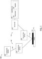
- FIG. 1 is a conceptual view of an inspection system 100 providing off-axis illumination and collection, in accordance with one or more embodiments of the present disclosure.
- the inspection system 100 includes an illumination source 102 to generate an illumination beam 104.
- the illumination beam 104 may include one or more selected wavelengths of light including, but not limited to, ultraviolet (UV), extreme ultraviolet (EUV), deep ultraviolet (DUV), or vacuum ultraviolet (VUV) radiation.
- UV ultraviolet
- EUV extreme ultraviolet
- DUV deep ultraviolet
- VUV vacuum ultraviolet
- at least a portion of a spectrum of the illumination beam 104 may include wavelengths below approximately 120 nanometers.
- at least a portion of a spectrum of the illumination beam 104 may include wavelengths associated with a lithography device suitable for semiconductor fabrication such as, but not limited to, 13.5 nm, 7 nm, or the like.
- the illumination source 102 may be any type of illumination source known in the art suitable for generating an optical illumination beam 104.
- the illumination source 102 includes a broadband plasma (BBP) illumination source.
- the illumination beam 104 may include radiation emitted by a plasma.
- a BBP illumination source 102 may include, but is not required to include, one or more pump sources (e.g., one or more lasers) configured to focus into the volume of a gas, causing energy to be absorbed by the gas in order to generate or sustain a plasma suitable for emitting radiation. Further, at least a portion of the plasma radiation may be utilized as the illumination beam 104.
- the illumination source 102 may include one or more lasers capable of emitting radiation at one or more selected wavelengths.
- the illumination source 102 directs the illumination beam 104 to a sample 106 via an illumination pathway 108.
- the illumination pathway 108 may include one or more illumination optics 110 suitable for directing, focusing, and/or shaping the illumination beam 104 on the sample 106.
- the illumination optics 110 may include one or more lenses, one or more focusing elements, or the like.
- the illumination optics 110 may include any combination of reflective, transmissive, or absorbing optical elements known in the art suitable for directing and/or focusing the illumination beam 104.
- the illumination optics 110 may include reflective optics suitable for directing and/or focusing low-wavelength light (e.g., EUV light, and the like) such as, but not limited to, flat mirrors or curved mirrors (e.g., elliptical mirrors, parabolic mirrors, or the like).
- reflective optics suitable for directing and/or focusing low-wavelength light e.g., EUV light, and the like
- flat mirrors or curved mirrors e.g., elliptical mirrors, parabolic mirrors, or the like.
- the sample 106 is disposed on a sample stage 112.
- the sample stage 112 may include any device suitable for positioning and/or scanning the sample 106 within the inspection system 100.
- the sample stage 112 may include any combination of linear translation stages, rotational stages, tip/tilt stages, or the like.
- the collection optics 120 may include any combination of reflective, transmissive, or absorbing optical elements known in the art suitable for directing and/or focusing the collected light 116.
- the illumination optics 110 may include reflective optics suitable for directing and/or focusing low-wavelength light (e.g., EUV light, and the like) such as, but not limited to, flat mirrors or curved mirrors (e.g., elliptical mirrors, parabolic mirrors, or the like).
- the detector 114 may include any type of detector known in the art suitable for measuring collected light 116 received from the sample 106.
- a detector 114 may include, but is not limited to, a CCD detector, a TDI detector, a photomultiplier tube (PMT), an avalanche photodiode (APD), or the like.
- a detector 114 may include a spectroscopic detector suitable for identifying wavelengths of radiation emanating from the sample 106.
- the collection pathway 118 may further include any number of additional collection pathway components to direct and/or shape the collected light 116 from the sample 106 including, but not limited to, one or more apertures, one or more apodizers, one or more polarizers, or one or more filters.
- the collection pathway components provide a range of angles within which light is collected from the sample 106 (e.g., an imaging pupil distribution).
- the inspection system 100 includes a controller 122.
- the controller 122 includes one or more processors 124 configured to execute program instructions maintained on a memory medium 126 (e.g., memory).
- the one or more processors 124 of controller 122 may execute any of the various process steps described throughout the present disclosure.
- the memory medium 126 may include any storage medium known in the art suitable for storing program instructions executable by the associated one or more processors 124.
- the memory medium 126 may include a non-transitory memory medium.
- the memory medium 126 may include, but is not limited to, a read-only memory, a random access memory, a magnetic or optical memory device (e.g., disk), a magnetic tape, a solid state drive and the like. It is further noted that memory medium 126 may be housed in a common controller housing with the one or more processors 124. In one embodiment, the memory medium 126 may be located remotely with respect to the physical location of the one or more processors 124 and controller 122.
- the one or more processors 124 of controller 122 may access a remote memory (e.g., server), accessible through a network (e.g., internet, intranet and the like). Therefore, the above description should not be interpreted as a limitation on the present invention but merely an illustration.
- the controller 122 may be communicatively coupled with any component of the inspection system 100 or any additional components outside of the inspection system 100.
- the controller 122 may be configured to receive data from a component such as, but not limited to, the detector 114.
- the controller 122 may receive any combination of raw data, processed data (e.g., inspection results), and/or partially-processed data.
- the controller 122 may perform processing steps based on the received data.
- the controller 122 may perform defect inspection steps such as, but not limited to, defect identification, classification, or sorting.
- controller 122 may include one or more controllers housed in a common housing or within multiple housings. In this way, any controller or combination of controllers may be separately packaged as a module suitable for integration into the inspection system 100.
- the controller 122 may operate as a centralized processing platform. In another instance, the controller 122 may be distributed such that portions of the controller 122 may be implemented in and/or housed in any combination of the inspection tools.
- the controller 122 may control and/or direct (e.g., via control signals) any component of the inspection system 100.
- any combination of elements of the illumination pathway 108 and/or the collection pathway 118 may be adjustable.
- the controller 122 may modify any combination of illumination conditions or imaging conditions such as, but not limited to, the illumination or imaging pupil distributions.
- the inspection system 100 may be configured as any type of inspection known in the art. Further, the inspection system 100 may be, but is not required to be, an EUV inspection system 100 suitable for interrogating a sample 106 with EUV light.
- the inspection system 100 is a photomask inspection system. Accordingly, a sample 106 interrogated by the inspection system may include a photomask (e.g., a reticle).
- the inspection system 100 is configured as an EUV mask blank inspection system. EUV-based mask blank inspection is described generally in U.S. Patent No. 8,711,346 to Stokowski, issued on April 29, 2014 , and U.S. Patent No.
- the inspection system 100 is configured as a wafer inspection system or a reticle inspection system.
- EUV Imaging is described generally in U.S. Patent No. 8,842,272 to Wack, issued on September 23, 2014 , which is incorporated herein by reference in the entirety.
- FIGS. 2 through 4 circular and non-circular pupil distributions for illumination and collected light (e.g., illumination and imaging pupil distributions) are described in greater detail.
- the illumination and/or imaging pupil distributions of FIGS. 2 through 4 may be implemented by an inspection system such as, but not limited to, the inspection system 100 illustrated in FIG. 1 . Further, the illumination and/or imaging pupil distributions of FIGS. 2 through 4 may be, but are not required to be, suitable for EUV inspection.
- photomask inspection and lithography with a photomask may be, but is not required to be, performed by different illumination and/or imaging pupil distributions.
- selection of a central point e.g., corresponding to a chief ray angle
- a size, and/or a shape of a pupil distribution may incorporate tradeoffs between throughput (e.g., etendue), coherence, and the like that may differ for different applications.
- an illumination pupil distribution and an imaging pupil distribution associated with the same application may or may not have the same characteristics (e.g., a size and/or shape of a pupil distribution).
- the numerical aperture e.g., a largest angle of incident or collected light
- the numerical aperture of the inspection system may be limited by physical sizes or focusing powers of system components (e.g., illumination optics 110, collection optics 120, or the like).
- the reflectivity of the sample 106 may vary as a function of angle such that illumination and/or collection beyond a cut-off angle may be inefficient and/or impractical.
- an illumination pupil distribution associated with an inspection system lie within a cut-off angle associated with a sample 106 to ensure efficient utilization of light (e.g., the illumination beam 104).
- the imaging pupil distribution may be more flexibly designed than the illumination pupil distribution. For example, illumination outside the cutoff angle may be inefficiently utilized.
- the imaging pupil distribution may include both reflected light (e.g., light at an equal, but opposite angle as incident light) and scattered light, which may emanate from the sample 106 at a wide range of angles. Accordingly, extending an imaging pupil distribution corresponding to angles beyond those of reflected light may increase the captured light signal and may increase the signal to noise ratio of a generated image. Further, the imaging pupil distribution may generally extend beyond the cut-off angle associated with the sample 106 without decreasing performance.
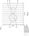
- FIG. 2 is a plot 200 of circular illumination and imaging pupil distributions for inspection and lithography of a sample 106 (e.g., a photomask), in accordance with one or more embodiments of the present disclosure.
- a sample 106 e.g., a photomask
- an angle of 0 represents a surface normal associated with the photomask
- distance from 0 represents the angle of incidence and/or collection with respect to the surface normal
- ⁇ X , ⁇ y represent azimuthal angles with respect to the photomask.
- ⁇ X and ⁇ y may correspond to X and Y directions, respectively, in a sample plane (e.g., a surface of the sample 106, a plane perpendicular to the surface normal, or the like).
- FIG. 2 is a plot 200 of circular illumination and imaging pupil distributions for inspection and lithography of a sample 106 (e.g., a photomask), in accordance with one or more embodiments of the present disclosure.
- FIG. 2 includes an illumination pupil distribution 202 and an imaging pupil distribution 204 for inspection (e.g., with the inspection system 100) as well as an illumination pupil distribution 206 and an imaging pupil distribution 208 for lithography.
- FIG. 2 illustrates the light cones associated with incident illumination and collected light used for imaging of a photomask in both inspection and lithography configurations.
- FIG. 2 illustrates a photomask coating cut-off angle 210 of approximately 14 degrees, represented as a circle centered around an angle of 0 (the surface normal).
- FIGS. 2 through 4 generally illustrate off-axis illumination and imaging of the sample 106 along the ⁇ X direction.
- a plane of incidence may be defined by the surface normal and a central ray of incident and/or collected light. It is recognized herein that for practical systems in which incident and/or collected light is represented as a cone (e.g., associated with a range of numerical apertures), a plane of incidence may be defined for each ray within the cone.
- a plane of incidence (e.g., an interaction plane) may be defined based on a central ray associated with the illumination beam 104 for any application (e.g., inspection, lithography, or the like).
- a plane of incidence associated with FIGS. 2 through 4 may be considered as a plane formed by the surface normal and the ⁇ X direction in angular space (or the X-direction on the sample 106).
- the imaging pupil distribution 204 for inspection may be, but is not required to be, centered in the plane of incidence.
- a distribution of a beam may typically not be represented as a step function, but may generally have tails. Additionally, a beam may include "hot spots" or irregularities.
- a center of an illumination and/or imaging pupil distribution may thus be determined by any technique known in the art. For example, a center of a pupil distribution may be determined based on, but not limited to, a location of an intensity peak, or a weighted intensity analysis.
- the illumination pupil distribution 206 and the imaging pupil distribution 208 for lithography are circular distributions (e.g., representing circular cones of illumination and/or collection of light). Further, the illumination pupil distribution 206 has a diameter of approximately 8 degrees and is centered at approximately +6 degrees along the ⁇ X direction, while the imaging pupil distribution 208 has a diameter of approximately 9 degrees and is centered at approximately -6 degrees the ⁇ X direction. In this regard, the illumination pupil distribution 206 and the imaging pupil distribution 208 for lithography may represent approximately symmetric off-axis illumination and collection of light along the ⁇ X direction, where the imaging pupil distribution is slightly larger than the illumination pupil distribution. Further, in this example, both the illumination pupil distribution 206 and the imaging pupil distribution 208 for lithography lie within the cut-off angle 210 of the photomask.
- the illumination pupil distribution 206 and the imaging pupil distribution 208 for lithography such as, but not limited to, the sizes, shapes, orientations, and positions of the distributions are provided solely for illustrative purposes and should not be interpreted as limiting. Further, the illumination pupil distribution 206 need not have the same size, shape, orientation, or the like as the imaging pupil distribution 208 for lithography.
- the illumination pupil distribution 202 and/or the imaging pupil distribution 204 associated with inspection of a sample 106 may also be circular such that the cones of illumination and/or collected light may be circular.
- the illumination pupil distribution 202 has a center point (e.g., corresponding to a chief ray angle) at approximately 7.5 degrees along the ⁇ X direction and a diameter of approximately 13 degrees such that the illumination pupil distribution 202 for inspection lies along an edge of, but is fully within, the cut-off angle 210.
- a center point e.g., corresponding to a chief ray angle
- the imaging pupil distribution 204 for inspection has a center point (e.g., corresponding to a chief ray angle) at approximately -9 degrees along the ⁇ X direction and a diameter of approximately 19 degrees. Accordingly, the imaging pupil distribution 204 for inspection may extend partially beyond the cut-off angle 210. As described previously herein, the imaging pupil distribution 204 for inspection may have a larger size than the illumination pupil distribution 202 for inspection to capture scattered light from the photomask in addition to reflected light.
- FIGS. 3 and 4 non-circular illumination and imaging pupil distributions, respectively, are described in greater detail.
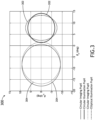
- FIG. 3 is a plot 300 illustrating two illumination pupil distributions for inspection with different shapes, in accordance with one or more embodiments of the present disclosure.
- FIG. 3 includes a non-circular illumination pupil distribution 302 as well as the illumination pupil distribution 202 for inspection and the imaging pupil distribution 204 for inspection illustrated in FIG. 2 .
- a non-circular illumination pupil distribution such as, but not limited to, the non-circular illumination pupil distribution 302 of FIG. 3 , may facilitate flexible design of the inspection system 100 that may provide increased sensitivity and/or throughput relative to a circular illumination pupil distribution without increasing the size, complexity and/or cost of optical components.
- illumination optics 110 may include one or more optical elements (e.g., mirrors, focusing elements, or the like) configured in an off-axis configuration such that the illumination beam 104 is not incident at a normal incidence angle.
- the illumination optics 110 may thus be sized to accommodate the projected size of the illumination beam 104 based on the angle of incidence of each element.
- many optical components are fabricated with circular dimensions for manufacturing and/or cost considerations.
- shaping portions of the illumination beam 104 along a direction perpendicular to a plane of incidence to provide a non-circular illumination pupil distribution 302 a direction perpendicular to a plane of incidence may utilize otherwise unused area on one or more illumination optics 110.
- a non-circular illumination pupil distribution 302 that extends further in directions outside the plane of incidence on the photomask (e.g., along the ⁇ Y direction) than in a direction within the plane of incidence (e.g., along the ⁇ X direction) may facilitate modification of the size, location, or shape of the imaging pupil distribution without increasing the size, complexity, and/or cost) of optical components.
- the non-circular illumination pupil distribution 302 may reduce the numerical aperture along the ⁇ X direction while maintaining a consistent etendue or throughput of the illumination beam 104 by extending along the ⁇ Y direction.
- This reduction of numerical aperture along the ⁇ X direction may allow for the position of the imaging pupil distribution 204 for inspection to be shifted towards the surface normal as indicated by a shifted imaging pupil distribution 304 in FIG. 3 .
- the shifted imaging pupil distribution 304 may provide increased performance in applications where reflectivity of the photomask (or a sample 106 more generally) increases for angles near normal incidence.
- size of the shifted imaging pupil distribution 304 may be increased to collect additional light from the sample (e.g., scattered light).
- a size of a non-circular illumination pupil distribution may be increased without increasing the size, complexity, and/or cost of the inspection system 100.
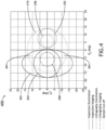
- FIG. 4 is a plot 400 illustrating imaging pupil distributions for inspection with different shapes, in accordance with one or more embodiments of the present disclosure.
- FIG. 4 includes a non-circular imaging pupil distribution 402 as well as the illumination pupil distribution 206 for lithography and imaging pupil distribution 204 illustrated for inspection in FIG. 2 .
- a non-circular imaging pupil distribution such as, but not limited to, the non-circular imaging pupil distribution 402 of FIG. 4 , may facilitate flexible design of the inspection system 100 that may provide increased sensitivity and/or throughput relative to a circular imaging pupil distribution without increasing the size, complexity and/or cost of optical components.
- collection optics 120 may include one or more optical elements (e.g., mirrors, focusing elements, or the like) configured in an off-axis configuration such that the collected light 116 is not incident at a normal incidence angle.
- the collection optics 120 may thus be sized to accommodate the projected size of the collected light 116 based on the range of angles at which light is collected from the sample.
- many optical components are fabricated with circular dimensions for manufacturing and/or cost considerations. Accordingly, it may be the case that shaping portions of the collected light 116 along a direction perpendicular to a plane of incidence to provide a non-circular imaging pupil distribution 402 may utilize otherwise unused area on one or more collection optics 120.
- the non-circular imaging pupil distribution 402 may extend further along the ⁇ Y direction than along the ⁇ X direction in order to capture additional light (e.g., scattered light) from the sample 106 without requiring additional size or complexity (and associated costs) than the imaging pupil distribution 204 for inspection.
- additional light e.g., scattered light
- scattered light may be collected (e.g., as the collected light 116) in regions 404 illustrated in FIG. 4 .
- a non-circular imaging pupil distribution may be sized along the ⁇ X direction to not exceed the cut-off angle 210.
- a non-circular imaging pupil distribution may be combined with a non-circular illumination pupil distribution (e.g., non-circular illumination pupil distribution 302).
- a non-circular illumination pupil distribution e.g., non-circular illumination pupil distribution 302
- the benefits of non-circular distribution for both illumination and imaging may be combined.
- the non-circular illumination pupil distribution 302 of FIG. 3 may be combined with the non-circular imaging pupil distribution 402 of FIG. 4 .
- the non-circular imaging pupil distribution 402 may be shifted along the ⁇ X (e.g., as described with respect to the imaging pupil distribution 304) to increase collected light 116 emanating from the sample 106 near the surface normal.
- a non-circular pupil distribution may generally have any non-circular shape.
- the non-circular illumination pupil distribution 302 and the non-circular imaging pupil distribution 402 in FIGS. 3 and 4 , respectively are illustrated as having elliptical shapes with major axes along the ⁇ Y direction (e.g., perpendicular to the plane of incidence including the surface normal and a ray at a center of the illumination pupil distribution).
- the non-circular illumination pupil distribution 302 and/or the non-circular imaging pupil distribution 402 may have an arbitrary non-circular shape.
- a non-circular pupil distribution may be formed using any combination of components of an inspection system 100 such as, but not limited to, one or more apertures.
- a non-circular illumination pupil distribution e.g., the non-circular illumination pupil distribution 302 in FIG. 3
- a non-circular imaging pupil distribution may be formed by one or more apertures in the collection pathway 118.
- FIG. 6 is a flow diagram illustrating steps performed in a method 600 for inspecting a sample. Applicant notes that the embodiments and enabling technologies described previously herein in the context of the inspection system 100 should be interpreted to extend to the method 600. It is further noted, however, that the method 600 is not limited to the architecture of the inspection system 100.
- the method 600 includes a step 606 of generating an image of the sample based on the collected light.
- a non-circular illumination pupil distribution may facilitate tuning the numerical apertures associated with the incident and/or collected light along the first direction (e.g., within a plane of incidence defined by a surface normal to the sample and a center of the illumination pupil distribution).
- the range of numerical apertures associated with the incident light e.g., the extent of the illumination pupil distribution along the first direction
- the angles of the incident light and/or the collected light along the first direction may be selected to be near the surface normal without sacrificing etendue of the incident light.
- performance may be increased relative to a circular illumination pupil distribution without increasing the size, complexity, and/or cost of associated optical components.
- a non-circular imaging pupil distribution may facilitate increased collection of scattered light to generate an image of the sample, which may provide increased signal strength and increased image quality relative to a circular illumination pupil without increasing the size, complexity, and/or cost of associated optical components.
- the size of pixels in a detector for generating an image of the sample and/or the magnification of optical components for collecting light from the sample (e.g., in step 604) and generating an image of the sample (e.g., in step 606) may be adjusted to provide uniform resolution of the image of the sample.
- steps 604 and 606 include imaging the sample with anamorphic magnification and square pixels to provide uniform image resolution along two orthogonal directions.
- steps 604 and 606 include imaging the sample with uniform magnification and rectangular pixels sized to provide uniform image resolution along two orthogonal directions.
- steps 604 and 606 include imaging the sample with anamorphic magnification and rectangular pixels sized to provide uniform image resolution along two orthogonal directions.
- any two components herein combined to achieve a particular functionality can be seen as “associated with” each other such that the desired functionality is achieved, irrespective of architectures or intermedial components.
- any two components so associated can also be viewed as being “connected” or “coupled” to each other to achieve the desired functionality, and any two components capable of being so associated can also be viewed as being “couplable” to each other to achieve the desired functionality.
- Specific examples of couplable include but are not limited to physically interactable and/or physically interacting components and/or wirelessly interactable and/or wirelessly interacting components and/or logically interactable and/or logically interacting components.
Landscapes
- Physics & Mathematics (AREA)
- General Physics & Mathematics (AREA)
- Health & Medical Sciences (AREA)
- Life Sciences & Earth Sciences (AREA)
- Chemical & Material Sciences (AREA)
- Analytical Chemistry (AREA)
- Biochemistry (AREA)
- General Health & Medical Sciences (AREA)
- Immunology (AREA)
- Pathology (AREA)
- Spectroscopy & Molecular Physics (AREA)
- Investigating Materials By The Use Of Optical Means Adapted For Particular Applications (AREA)
- Preparing Plates And Mask In Photomechanical Process (AREA)
Applications Claiming Priority (4)
| Application Number | Priority Date | Filing Date | Title |
|---|---|---|---|
| US201962793027P | 2019-01-16 | 2019-01-16 | |
| US16/258,118 US11112691B2 (en) | 2019-01-16 | 2019-01-25 | Inspection system with non-circular pupil |
| EP20741842.7A EP3891493A4 (de) | 2019-01-16 | 2020-01-09 | Inspektionssystem mit unrunder pupille |
| PCT/US2020/012817 WO2020150061A1 (en) | 2019-01-16 | 2020-01-09 | Inspection system with non-circular pupil |
Related Parent Applications (1)
| Application Number | Title | Priority Date | Filing Date |
|---|---|---|---|
| EP20741842.7A Division EP3891493A4 (de) | 2019-01-16 | 2020-01-09 | Inspektionssystem mit unrunder pupille |
Publications (2)
| Publication Number | Publication Date |
|---|---|
| EP4524653A2 true EP4524653A2 (de) | 2025-03-19 |
| EP4524653A3 EP4524653A3 (de) | 2025-06-18 |
Family
ID=71516612
Family Applications (2)
| Application Number | Title | Priority Date | Filing Date |
|---|---|---|---|
| EP25155396.2A Pending EP4524653A3 (de) | 2019-01-16 | 2020-01-09 | Inspektionssystem mit nichtrundförmiger puppe |
| EP20741842.7A Pending EP3891493A4 (de) | 2019-01-16 | 2020-01-09 | Inspektionssystem mit unrunder pupille |
Family Applications After (1)
| Application Number | Title | Priority Date | Filing Date |
|---|---|---|---|
| EP20741842.7A Pending EP3891493A4 (de) | 2019-01-16 | 2020-01-09 | Inspektionssystem mit unrunder pupille |
Country Status (6)
| Country | Link |
|---|---|
| US (1) | US11112691B2 (de) |
| EP (2) | EP4524653A3 (de) |
| JP (2) | JP7637054B2 (de) |
| KR (2) | KR20250111392A (de) |
| TW (1) | TWI851644B (de) |
| WO (1) | WO2020150061A1 (de) |
Families Citing this family (9)
| Publication number | Priority date | Publication date | Assignee | Title |
|---|---|---|---|---|
| US11557031B2 (en) * | 2019-11-21 | 2023-01-17 | Kla Corporation | Integrated multi-tool reticle inspection |
| US11614684B2 (en) * | 2020-09-08 | 2023-03-28 | Taiwan Semiconductor Manufacturing Company Ltd. | Photomask inspection method and apparatus thereof |
| US11609506B2 (en) | 2021-04-21 | 2023-03-21 | Kla Corporation | System and method for lateral shearing interferometry in an inspection tool |
| US20240003827A1 (en) * | 2022-06-30 | 2024-01-04 | Taiwan Semiconductor Manufacturing Company | Systems and methods for actinic mask inspection and review in vacuum |
| JP2024127783A (ja) * | 2023-03-09 | 2024-09-20 | レーザーテック株式会社 | 照明装置及び照明方法 |
| US20250044679A1 (en) * | 2023-07-31 | 2025-02-06 | Kla Corporation | Pupil filter with spatially-varying transmission |
| DE102024111144A1 (de) * | 2024-04-22 | 2025-10-23 | Carl Zeiss Smt Gmbh | Verfahren zum Betreiben einer Maskeninspektionsvorrichtung, EUV-Kamera, Maskeninspektionsvorrichtung, Computerprogrammprodukt |
| US20250383294A1 (en) * | 2024-06-18 | 2025-12-18 | Kla Corporation | Speckle noise reduction using pupil masks |
| US20260056397A1 (en) * | 2024-08-22 | 2026-02-26 | Kla Corporation | Wolter mirror assembly |
Citations (3)
| Publication number | Priority date | Publication date | Assignee | Title |
|---|---|---|---|---|
| US8711346B2 (en) | 2009-06-19 | 2014-04-29 | Kla-Tencor Corporation | Inspection systems and methods for detecting defects on extreme ultraviolet mask blanks |
| US8785082B2 (en) | 2011-03-15 | 2014-07-22 | Kla-Tencor Corporation | Method and apparatus for inspecting a reflective lithographic mask blank and improving mask quality |
| US8842272B2 (en) | 2011-01-11 | 2014-09-23 | Kla-Tencor Corporation | Apparatus for EUV imaging and methods of using same |
Family Cites Families (24)
| Publication number | Priority date | Publication date | Assignee | Title |
|---|---|---|---|---|
| JPS636854A (ja) * | 1986-06-27 | 1988-01-12 | Hitachi Ltd | 異物検査装置 |
| US6628370B1 (en) * | 1996-11-25 | 2003-09-30 | Mccullough Andrew W. | Illumination system with spatially controllable partial coherence compensating for line width variances in a photolithographic system |
| US6643390B1 (en) * | 2000-04-19 | 2003-11-04 | Polaroid Corporation | Compact fingerprint identification device |
| DE10112947A1 (de) * | 2001-03-17 | 2002-09-26 | Zeiss Carl Jena Gmbh | Verfahren zur Auswertung von Schichtbildern |
| FR2917844A1 (fr) * | 2007-06-20 | 2008-12-26 | Vincent Lauer | Dispositif interferometrique |
| US7796804B2 (en) * | 2007-07-20 | 2010-09-14 | Kla-Tencor Corp. | Methods for generating a standard reference die for use in a die to standard reference die inspection and methods for inspecting a wafer |
| US8451427B2 (en) | 2007-09-14 | 2013-05-28 | Nikon Corporation | Illumination optical system, exposure apparatus, optical element and manufacturing method thereof, and device manufacturing method |
| WO2011065374A1 (ja) * | 2009-11-24 | 2011-06-03 | 株式会社ニコン | 結像光学系、露光装置、およびデバイス製造方法 |
| US9319578B2 (en) * | 2012-10-24 | 2016-04-19 | Alcatel Lucent | Resolution and focus enhancement |
| US9279774B2 (en) * | 2011-07-12 | 2016-03-08 | Kla-Tencor Corp. | Wafer inspection |
| JP5751994B2 (ja) * | 2011-09-02 | 2015-07-22 | ルネサスエレクトロニクス株式会社 | マスクブランクの欠陥検査方法 |
| JP6120001B2 (ja) | 2011-10-24 | 2017-04-26 | 株式会社ニコン | 照明光学系、露光装置、およびデバイス製造方法 |
| US20130148115A1 (en) * | 2011-12-12 | 2013-06-13 | Yoav Berlatzky | Optical system and method for inspection of patterned samples |
| JP5865738B2 (ja) | 2012-03-13 | 2016-02-17 | 株式会社日立ハイテクノロジーズ | 欠陥検査方法及びその装置 |
| US9116103B2 (en) | 2013-01-14 | 2015-08-25 | Kla-Tencor Corporation | Multiple angles of incidence semiconductor metrology systems and methods |
| DE102013204445A1 (de) * | 2013-03-14 | 2014-09-18 | Carl Zeiss Smt Gmbh | Vergrößernde abbildende Optik sowie EUV-Maskeninspektionssystem mit einer derartigen abbildenden Optik |
| KR102202523B1 (ko) * | 2013-07-18 | 2021-01-13 | 케이엘에이 코포레이션 | 스캐터로메트리 측정들을 위한 조명 구성들 |
| JP6215009B2 (ja) * | 2013-11-15 | 2017-10-18 | 株式会社東芝 | 撮像装置及び撮像方法 |
| NL2014179A (en) * | 2014-02-24 | 2015-08-25 | Asml Netherlands Bv | Lithographic system. |
| DE102014214257A1 (de) * | 2014-07-22 | 2016-01-28 | Carl Zeiss Smt Gmbh | Verfahren zum dreidimensionalen Vermessen eines 3D-Luftbildes einer Lithografiemaske |
| WO2016012425A2 (de) * | 2014-07-22 | 2016-01-28 | Carl Zeiss Smt Gmbh | Abbildende optik für ein metrologiesystem zur untersuchung einer lithographiemaske |
| DE102015216528A1 (de) | 2015-08-28 | 2017-03-02 | Carl Zeiss Smt Gmbh | Beleuchtungssystem für EUV-Projektionsbelichtungsanlage, EUV-Projektionsbelichtungsanlage mit Beleuchtungssystem und Verfahren zum Betreiben einer EUV-Projektionsbelichtungsanlage |
| WO2018014046A1 (en) * | 2016-07-15 | 2018-01-18 | Light Field Lab, Inc. | Encoded energy waveguides for holographic super resolution |
| WO2018081144A1 (en) * | 2016-10-24 | 2018-05-03 | Kla-Tencor Corporation | Process module(s) integrated into a metrology and/or inspection tool |
-
2019
- 2019-01-25 US US16/258,118 patent/US11112691B2/en active Active
-
2020
- 2020-01-03 TW TW109100140A patent/TWI851644B/zh active
- 2020-01-09 EP EP25155396.2A patent/EP4524653A3/de active Pending
- 2020-01-09 JP JP2021539928A patent/JP7637054B2/ja active Active
- 2020-01-09 KR KR1020257023305A patent/KR20250111392A/ko active Pending
- 2020-01-09 WO PCT/US2020/012817 patent/WO2020150061A1/en not_active Ceased
- 2020-01-09 EP EP20741842.7A patent/EP3891493A4/de active Pending
- 2020-01-09 KR KR1020217024477A patent/KR102835353B1/ko active Active
-
2025
- 2025-01-14 JP JP2025004817A patent/JP7792027B2/ja active Active
Patent Citations (3)
| Publication number | Priority date | Publication date | Assignee | Title |
|---|---|---|---|---|
| US8711346B2 (en) | 2009-06-19 | 2014-04-29 | Kla-Tencor Corporation | Inspection systems and methods for detecting defects on extreme ultraviolet mask blanks |
| US8842272B2 (en) | 2011-01-11 | 2014-09-23 | Kla-Tencor Corporation | Apparatus for EUV imaging and methods of using same |
| US8785082B2 (en) | 2011-03-15 | 2014-07-22 | Kla-Tencor Corporation | Method and apparatus for inspecting a reflective lithographic mask blank and improving mask quality |
Also Published As
| Publication number | Publication date |
|---|---|
| US20200225574A1 (en) | 2020-07-16 |
| KR20250111392A (ko) | 2025-07-22 |
| US11112691B2 (en) | 2021-09-07 |
| WO2020150061A1 (en) | 2020-07-23 |
| JP2025065566A (ja) | 2025-04-18 |
| KR102835353B1 (ko) | 2025-07-16 |
| EP3891493A4 (de) | 2022-09-07 |
| TWI851644B (zh) | 2024-08-11 |
| JP2022517067A (ja) | 2022-03-04 |
| JP7792027B2 (ja) | 2025-12-24 |
| EP4524653A3 (de) | 2025-06-18 |
| TW202104882A (zh) | 2021-02-01 |
| JP7637054B2 (ja) | 2025-02-27 |
| KR20210107860A (ko) | 2021-09-01 |
| EP3891493A1 (de) | 2021-10-13 |
Similar Documents
| Publication | Publication Date | Title |
|---|---|---|
| US11112691B2 (en) | Inspection system with non-circular pupil | |
| JP5749641B2 (ja) | 光学検査システム及び方法 | |
| US7345825B2 (en) | Beam delivery system for laser dark-field illumination in a catadioptric optical system | |
| KR102367236B1 (ko) | 레이저 암시야 시스템에서 반점을 억제하는 방법 및 장치 | |
| JP2015222434A (ja) | 小型カタジオプトリック型対物系を用いた検査システム | |
| US20220155693A1 (en) | System and Method for Error Reduction for Metrology Measurements | |
| KR20120073270A (ko) | 계측 시스템 및 계측 방법 | |
| US20150192459A1 (en) | Extreme ultra-violet (euv) inspection systems | |
| JP2023553053A (ja) | オンザフライ散乱計測オーバーレイ計測ターゲット | |
| JP2007171640A (ja) | 散乱光の角度分布を使ったマスクブランクの欠陥の検出および特性評価 | |
| JP2024059661A (ja) | 計測光に関する物体の反射率を計測するための方法およびその方法を実行するための計量システム | |
| US20050146719A1 (en) | Method and apparatus for illuminating a substrate during inspection | |
| US9151718B2 (en) | Illumination system with time multiplexed sources for reticle inspection | |
| TWI899213B (zh) | 污染識別度量衡系統、微影設備及其方法 | |
| US20260056460A1 (en) | Apodization measurement optics and measurement method for euv reticle inspection tool | |
| US20250102446A1 (en) | Optical systems and methods of providing a coupling mirror to an optical system | |
| US20260044946A1 (en) | Actinic run time system diagnostics of euv reticle inspection and imaging systems using miniaturized euv calibration targets | |
| TW202615962A (zh) | 用於極紫外線光罩檢測工具之跡變測量光學件及測量方法 | |
| WO2025029409A1 (en) | Pupil filter with spatially-varying transmission |
Legal Events
| Date | Code | Title | Description |
|---|---|---|---|
| PUAI | Public reference made under article 153(3) epc to a published international application that has entered the european phase |
Free format text: ORIGINAL CODE: 0009012 |
|
| STAA | Information on the status of an ep patent application or granted ep patent |
Free format text: STATUS: THE APPLICATION HAS BEEN PUBLISHED |
|
| AC | Divisional application: reference to earlier application |
Ref document number: 3891493 Country of ref document: EP Kind code of ref document: P |
|
| AK | Designated contracting states |
Kind code of ref document: A2 Designated state(s): AL AT BE BG CH CY CZ DE DK EE ES FI FR GB GR HR HU IE IS IT LI LT LU LV MC MK MT NL NO PL PT RO RS SE SI SK SM TR |
|
| REG | Reference to a national code |
Ref country code: DE Ref legal event code: R079 Free format text: PREVIOUS MAIN CLASS: G03F0001840000 Ipc: G01N0021956000 |
|
| PUAL | Search report despatched |
Free format text: ORIGINAL CODE: 0009013 |
|
| AK | Designated contracting states |
Kind code of ref document: A3 Designated state(s): AL AT BE BG CH CY CZ DE DK EE ES FI FR GB GR HR HU IE IS IT LI LT LU LV MC MK MT NL NO PL PT RO RS SE SI SK SM TR |
|
| RIC1 | Information provided on ipc code assigned before grant |
Ipc: G03F 1/84 20120101ALI20250514BHEP Ipc: G03F 1/24 20120101ALI20250514BHEP Ipc: G01N 21/33 20060101ALI20250514BHEP Ipc: G01N 21/88 20060101ALI20250514BHEP Ipc: G01N 21/956 20060101AFI20250514BHEP |
|
| STAA | Information on the status of an ep patent application or granted ep patent |
Free format text: STATUS: REQUEST FOR EXAMINATION WAS MADE |
|
| 17P | Request for examination filed |
Effective date: 20251217 |