EP4521429A2 - Elektrische komponenten mit spulen und verfahren zur herstellung davon durch 3d-drucken - Google Patents
Elektrische komponenten mit spulen und verfahren zur herstellung davon durch 3d-drucken Download PDFInfo
- Publication number
- EP4521429A2 EP4521429A2 EP24194993.2A EP24194993A EP4521429A2 EP 4521429 A2 EP4521429 A2 EP 4521429A2 EP 24194993 A EP24194993 A EP 24194993A EP 4521429 A2 EP4521429 A2 EP 4521429A2
- Authority
- EP
- European Patent Office
- Prior art keywords
- magnetic
- printed
- turns
- printing
- conductive
- Prior art date
- Legal status (The legal status is an assumption and is not a legal conclusion. Google has not performed a legal analysis and makes no representation as to the accuracy of the status listed.)
- Granted
Links
Images


Classifications
-
- H—ELECTRICITY
- H01—ELECTRIC ELEMENTS
- H01F—MAGNETS; INDUCTANCES; TRANSFORMERS; SELECTION OF MATERIALS FOR THEIR MAGNETIC PROPERTIES
- H01F41/00—Apparatus or processes specially adapted for manufacturing or assembling magnets, inductances or transformers; Apparatus or processes specially adapted for manufacturing materials characterised by their magnetic properties
- H01F41/02—Apparatus or processes specially adapted for manufacturing or assembling magnets, inductances or transformers; Apparatus or processes specially adapted for manufacturing materials characterised by their magnetic properties for manufacturing cores, coils, or magnets
- H01F41/0206—Manufacturing of magnetic cores by mechanical means
-
- B—PERFORMING OPERATIONS; TRANSPORTING
- B29—WORKING OF PLASTICS; WORKING OF SUBSTANCES IN A PLASTIC STATE IN GENERAL
- B29C—SHAPING OR JOINING OF PLASTICS; SHAPING OF MATERIAL IN A PLASTIC STATE, NOT OTHERWISE PROVIDED FOR; AFTER-TREATMENT OF THE SHAPED PRODUCTS, e.g. REPAIRING
- B29C64/00—Additive manufacturing, i.e. manufacturing of three-dimensional [3D] objects by additive deposition, additive agglomeration or additive layering, e.g. by 3D printing, stereolithography or selective laser sintering
- B29C64/10—Processes of additive manufacturing
-
- A—HUMAN NECESSITIES
- A61—MEDICAL OR VETERINARY SCIENCE; HYGIENE
- A61B—DIAGNOSIS; SURGERY; IDENTIFICATION
- A61B5/00—Measuring for diagnostic purposes; Identification of persons
- A61B5/06—Devices, other than using radiation, for detecting or locating foreign bodies ; Determining position of diagnostic devices within or on the body of the patient
- A61B5/061—Determining position of a probe within the body employing means separate from the probe, e.g. sensing internal probe position employing impedance electrodes on the surface of the body
- A61B5/062—Determining position of a probe within the body employing means separate from the probe, e.g. sensing internal probe position employing impedance electrodes on the surface of the body using magnetic field
-
- A—HUMAN NECESSITIES
- A61—MEDICAL OR VETERINARY SCIENCE; HYGIENE
- A61B—DIAGNOSIS; SURGERY; IDENTIFICATION
- A61B5/00—Measuring for diagnostic purposes; Identification of persons
- A61B5/06—Devices, other than using radiation, for detecting or locating foreign bodies ; Determining position of diagnostic devices within or on the body of the patient
- A61B5/065—Determining position of the probe employing exclusively positioning means located on or in the probe, e.g. using position sensors arranged on the probe
-
- A—HUMAN NECESSITIES
- A61—MEDICAL OR VETERINARY SCIENCE; HYGIENE
- A61B—DIAGNOSIS; SURGERY; IDENTIFICATION
- A61B5/00—Measuring for diagnostic purposes; Identification of persons
- A61B5/68—Arrangements of detecting, measuring or recording means, e.g. sensors, in relation to patient
- A61B5/6846—Arrangements of detecting, measuring or recording means, e.g. sensors, in relation to patient specially adapted to be brought in contact with an internal body part, i.e. invasive
- A61B5/6885—Monitoring or controlling sensor contact pressure
-
- A—HUMAN NECESSITIES
- A61—MEDICAL OR VETERINARY SCIENCE; HYGIENE
- A61M—DEVICES FOR INTRODUCING MEDIA INTO, OR ONTO, THE BODY; DEVICES FOR TRANSDUCING BODY MEDIA OR FOR TAKING MEDIA FROM THE BODY; DEVICES FOR PRODUCING OR ENDING SLEEP OR STUPOR
- A61M25/00—Catheters; Hollow probes
- A61M25/01—Introducing, guiding, advancing, emplacing or holding catheters
- A61M25/0105—Steering means as part of the catheter or advancing means; Markers for positioning
- A61M25/0127—Magnetic means; Magnetic markers
-
- B—PERFORMING OPERATIONS; TRANSPORTING
- B22—CASTING; POWDER METALLURGY
- B22F—WORKING METALLIC POWDER; MANUFACTURE OF ARTICLES FROM METALLIC POWDER; MAKING METALLIC POWDER; APPARATUS OR DEVICES SPECIALLY ADAPTED FOR METALLIC POWDER
- B22F10/00—Additive manufacturing of workpieces or articles from metallic powder
- B22F10/10—Formation of a green body
- B22F10/12—Formation of a green body by photopolymerisation, e.g. stereolithography [SLA] or digital light processing [DLP]
-
- B—PERFORMING OPERATIONS; TRANSPORTING
- B22—CASTING; POWDER METALLURGY
- B22F—WORKING METALLIC POWDER; MANUFACTURE OF ARTICLES FROM METALLIC POWDER; MAKING METALLIC POWDER; APPARATUS OR DEVICES SPECIALLY ADAPTED FOR METALLIC POWDER
- B22F5/00—Manufacture of workpieces or articles from metallic powder characterised by the special shape of the product
- B22F5/10—Manufacture of workpieces or articles from metallic powder characterised by the special shape of the product of articles with cavities or holes, not otherwise provided for in the preceding subgroups
-
- B—PERFORMING OPERATIONS; TRANSPORTING
- B33—ADDITIVE MANUFACTURING TECHNOLOGY
- B33Y—ADDITIVE MANUFACTURING, i.e. MANUFACTURING OF THREE-DIMENSIONAL [3D] OBJECTS BY ADDITIVE DEPOSITION, ADDITIVE AGGLOMERATION OR ADDITIVE LAYERING, e.g. BY 3D PRINTING, STEREOLITHOGRAPHY OR SELECTIVE LASER SINTERING
- B33Y10/00—Processes of additive manufacturing
-
- B—PERFORMING OPERATIONS; TRANSPORTING
- B33—ADDITIVE MANUFACTURING TECHNOLOGY
- B33Y—ADDITIVE MANUFACTURING, i.e. MANUFACTURING OF THREE-DIMENSIONAL [3D] OBJECTS BY ADDITIVE DEPOSITION, ADDITIVE AGGLOMERATION OR ADDITIVE LAYERING, e.g. BY 3D PRINTING, STEREOLITHOGRAPHY OR SELECTIVE LASER SINTERING
- B33Y40/00—Auxiliary operations or equipment, e.g. for material handling
- B33Y40/20—Post-treatment, e.g. curing, coating or polishing
-
- B—PERFORMING OPERATIONS; TRANSPORTING
- B33—ADDITIVE MANUFACTURING TECHNOLOGY
- B33Y—ADDITIVE MANUFACTURING, i.e. MANUFACTURING OF THREE-DIMENSIONAL [3D] OBJECTS BY ADDITIVE DEPOSITION, ADDITIVE AGGLOMERATION OR ADDITIVE LAYERING, e.g. BY 3D PRINTING, STEREOLITHOGRAPHY OR SELECTIVE LASER SINTERING
- B33Y70/00—Materials specially adapted for additive manufacturing
- B33Y70/10—Composites of different types of material, e.g. mixtures of ceramics and polymers or mixtures of metals and biomaterials
-
- B—PERFORMING OPERATIONS; TRANSPORTING
- B33—ADDITIVE MANUFACTURING TECHNOLOGY
- B33Y—ADDITIVE MANUFACTURING, i.e. MANUFACTURING OF THREE-DIMENSIONAL [3D] OBJECTS BY ADDITIVE DEPOSITION, ADDITIVE AGGLOMERATION OR ADDITIVE LAYERING, e.g. BY 3D PRINTING, STEREOLITHOGRAPHY OR SELECTIVE LASER SINTERING
- B33Y80/00—Products made by additive manufacturing
-
- G—PHYSICS
- G01—MEASURING; TESTING
- G01D—MEASURING NOT SPECIALLY ADAPTED FOR A SPECIFIC VARIABLE; ARRANGEMENTS FOR MEASURING TWO OR MORE VARIABLES NOT COVERED IN A SINGLE OTHER SUBCLASS; TARIFF METERING APPARATUS; MEASURING OR TESTING NOT OTHERWISE PROVIDED FOR
- G01D5/00—Mechanical means for transferring the output of a sensing member; Means for converting the output of a sensing member to another variable where the form or nature of the sensing member does not constrain the means for converting; Transducers not specially adapted for a specific variable
- G01D5/12—Mechanical means for transferring the output of a sensing member; Means for converting the output of a sensing member to another variable where the form or nature of the sensing member does not constrain the means for converting; Transducers not specially adapted for a specific variable using electric or magnetic means
- G01D5/14—Mechanical means for transferring the output of a sensing member; Means for converting the output of a sensing member to another variable where the form or nature of the sensing member does not constrain the means for converting; Transducers not specially adapted for a specific variable using electric or magnetic means influencing the magnitude of a current or voltage
- G01D5/20—Mechanical means for transferring the output of a sensing member; Means for converting the output of a sensing member to another variable where the form or nature of the sensing member does not constrain the means for converting; Transducers not specially adapted for a specific variable using electric or magnetic means influencing the magnitude of a current or voltage by varying inductance, e.g. by a movable armature
-
- G—PHYSICS
- G01—MEASURING; TESTING
- G01R—MEASURING ELECTRIC VARIABLES; MEASURING MAGNETIC VARIABLES
- G01R33/00—Arrangements or instruments for measuring magnetic variables
- G01R33/0005—Geometrical arrangement of magnetic sensor elements; Apparatus combining different magnetic sensor types
-
- G—PHYSICS
- G01—MEASURING; TESTING
- G01R—MEASURING ELECTRIC VARIABLES; MEASURING MAGNETIC VARIABLES
- G01R33/00—Arrangements or instruments for measuring magnetic variables
- G01R33/0052—Manufacturing aspects; Manufacturing of single devices, i.e. of semiconductor magnetic sensor chips
-
- G—PHYSICS
- G01—MEASURING; TESTING
- G01R—MEASURING ELECTRIC VARIABLES; MEASURING MAGNETIC VARIABLES
- G01R33/00—Arrangements or instruments for measuring magnetic variables
- G01R33/02—Measuring direction or magnitude of magnetic fields or magnetic flux
-
- H—ELECTRICITY
- H01—ELECTRIC ELEMENTS
- H01F—MAGNETS; INDUCTANCES; TRANSFORMERS; SELECTION OF MATERIALS FOR THEIR MAGNETIC PROPERTIES
- H01F17/00—Fixed inductances of the signal type
- H01F17/0006—Printed inductances
- H01F17/0013—Printed inductances with stacked layers
-
- H—ELECTRICITY
- H01—ELECTRIC ELEMENTS
- H01F—MAGNETS; INDUCTANCES; TRANSFORMERS; SELECTION OF MATERIALS FOR THEIR MAGNETIC PROPERTIES
- H01F41/00—Apparatus or processes specially adapted for manufacturing or assembling magnets, inductances or transformers; Apparatus or processes specially adapted for manufacturing materials characterised by their magnetic properties
- H01F41/02—Apparatus or processes specially adapted for manufacturing or assembling magnets, inductances or transformers; Apparatus or processes specially adapted for manufacturing materials characterised by their magnetic properties for manufacturing cores, coils, or magnets
- H01F41/04—Apparatus or processes specially adapted for manufacturing or assembling magnets, inductances or transformers; Apparatus or processes specially adapted for manufacturing materials characterised by their magnetic properties for manufacturing cores, coils, or magnets for manufacturing coils
- H01F41/041—Printed circuit coils
- H01F41/043—Printed circuit coils by thick film techniques
-
- H—ELECTRICITY
- H01—ELECTRIC ELEMENTS
- H01F—MAGNETS; INDUCTANCES; TRANSFORMERS; SELECTION OF MATERIALS FOR THEIR MAGNETIC PROPERTIES
- H01F41/00—Apparatus or processes specially adapted for manufacturing or assembling magnets, inductances or transformers; Apparatus or processes specially adapted for manufacturing materials characterised by their magnetic properties
- H01F41/02—Apparatus or processes specially adapted for manufacturing or assembling magnets, inductances or transformers; Apparatus or processes specially adapted for manufacturing materials characterised by their magnetic properties for manufacturing cores, coils, or magnets
- H01F41/04—Apparatus or processes specially adapted for manufacturing or assembling magnets, inductances or transformers; Apparatus or processes specially adapted for manufacturing materials characterised by their magnetic properties for manufacturing cores, coils, or magnets for manufacturing coils
- H01F41/12—Insulating of windings
- H01F41/122—Insulating between turns or between winding layers
-
- H—ELECTRICITY
- H01—ELECTRIC ELEMENTS
- H01F—MAGNETS; INDUCTANCES; TRANSFORMERS; SELECTION OF MATERIALS FOR THEIR MAGNETIC PROPERTIES
- H01F5/00—Coils
-
- H—ELECTRICITY
- H01—ELECTRIC ELEMENTS
- H01F—MAGNETS; INDUCTANCES; TRANSFORMERS; SELECTION OF MATERIALS FOR THEIR MAGNETIC PROPERTIES
- H01F5/00—Coils
- H01F5/04—Arrangements of electric connections to coils, e.g. leads
-
- H—ELECTRICITY
- H01—ELECTRIC ELEMENTS
- H01F—MAGNETS; INDUCTANCES; TRANSFORMERS; SELECTION OF MATERIALS FOR THEIR MAGNETIC PROPERTIES
- H01F5/00—Coils
- H01F5/06—Insulation of windings
-
- A—HUMAN NECESSITIES
- A61—MEDICAL OR VETERINARY SCIENCE; HYGIENE
- A61B—DIAGNOSIS; SURGERY; IDENTIFICATION
- A61B34/00—Computer-aided surgery; Manipulators or robots specially adapted for use in surgery
- A61B34/20—Surgical navigation systems; Devices for tracking or guiding surgical instruments, e.g. for frameless stereotaxis
- A61B2034/2046—Tracking techniques
- A61B2034/2051—Electromagnetic tracking systems
-
- A—HUMAN NECESSITIES
- A61—MEDICAL OR VETERINARY SCIENCE; HYGIENE
- A61B—DIAGNOSIS; SURGERY; IDENTIFICATION
- A61B90/00—Instruments, implements or accessories specially adapted for surgery or diagnosis and not covered by any of the groups A61B1/00 - A61B50/00, e.g. for luxation treatment or for protecting wound edges
- A61B90/39—Markers, e.g. radio-opaque or breast lesions markers
- A61B2090/3983—Reference marker arrangements for use with image guided surgery
-
- A—HUMAN NECESSITIES
- A61—MEDICAL OR VETERINARY SCIENCE; HYGIENE
- A61B—DIAGNOSIS; SURGERY; IDENTIFICATION
- A61B2562/00—Details of sensors; Constructional details of sensor housings or probes; Accessories for sensors
- A61B2562/02—Details of sensors specially adapted for in-vivo measurements
- A61B2562/0223—Magnetic field sensors
-
- A—HUMAN NECESSITIES
- A61—MEDICAL OR VETERINARY SCIENCE; HYGIENE
- A61B—DIAGNOSIS; SURGERY; IDENTIFICATION
- A61B2562/00—Details of sensors; Constructional details of sensor housings or probes; Accessories for sensors
- A61B2562/12—Manufacturing methods specially adapted for producing sensors for in-vivo measurements
-
- A—HUMAN NECESSITIES
- A61—MEDICAL OR VETERINARY SCIENCE; HYGIENE
- A61B—DIAGNOSIS; SURGERY; IDENTIFICATION
- A61B5/00—Measuring for diagnostic purposes; Identification of persons
- A61B5/68—Arrangements of detecting, measuring or recording means, e.g. sensors, in relation to patient
- A61B5/6846—Arrangements of detecting, measuring or recording means, e.g. sensors, in relation to patient specially adapted to be brought in contact with an internal body part, i.e. invasive
- A61B5/6847—Arrangements of detecting, measuring or recording means, e.g. sensors, in relation to patient specially adapted to be brought in contact with an internal body part, i.e. invasive mounted on an invasive device
- A61B5/6852—Catheters
-
- B—PERFORMING OPERATIONS; TRANSPORTING
- B22—CASTING; POWDER METALLURGY
- B22F—WORKING METALLIC POWDER; MANUFACTURE OF ARTICLES FROM METALLIC POWDER; MAKING METALLIC POWDER; APPARATUS OR DEVICES SPECIALLY ADAPTED FOR METALLIC POWDER
- B22F2998/00—Supplementary information concerning processes or compositions relating to powder metallurgy
- B22F2998/10—Processes characterised by the sequence of their steps
-
- C—CHEMISTRY; METALLURGY
- C22—METALLURGY; FERROUS OR NON-FERROUS ALLOYS; TREATMENT OF ALLOYS OR NON-FERROUS METALS
- C22C—ALLOYS
- C22C2202/00—Physical properties
- C22C2202/02—Magnetic
Definitions
- the present invention is in the field of magnetic field sensors and specifically relates to techniques of fabricating electric components including coils which are suitable for magnetic-field-based position sensing, particularly for sensing the positions of medical devices.
- a catheter/probe In various therapeutic and diagnostic procedures, a catheter/probe is inserted into a patient's body (e.g., chamber of the heart) and to be brought into contact with a body tissue there. Typically, in such procedures, it is necessary to determine the catheter's location within the body (i.e., the location at which a distal tip of the catheter engages the body tissue) as well as the pressure applied thereby to the tissue.
- Catheters having integrated location and pressure sensors for sensing the location of the catheter and the pressure/force applied thereby at the contact region with the tissue are generally known. Such catheters typically utilize inductive coils for determining the location of the catheter within the body and/or the pressure/force applied thereby to a body tissue it engages with.
- U.S. patent No. U.S.8,535,308 and U.S. patent application No. U.S. 2020/015693 which are both assigned to the assignee of the present Application, disclose for example configurations of such catheters utilizing sensory circuits having several coils, for sensing the location and orientation of the catheter body, as well as the force applied thereby at the interface with the tissue.
- the location and force sensors generally utilize miniature wire-winded coils to which a ferrite core may be manually inserted with an open magnetic circuit configuration in order to yield sufficient induced-voltages suitable for location and force sensing of the catheter components.
- These conventional techniques are however time consuming and costly and involve delicate manual operations for fitting of the coils within the small dimensions of the catheters body.
- the present invention provides a novel and inventive electric component including one or more coils suitable for use as/in magnetic field sensor of a magnetic-field-based positioning system. Moreover, the present invention provides a novel and inventive method of fabrication of the electric components including such coil(s) utilizing 3D printing technique. In embodiments the electric component may be fabricated with coil(s) of compact dimensions while providing relatively high induced-voltage in response to sensed magnetic fields, and is therefore particularly suited for use as a position sensor for sensing the positions of compact medical device, such as catheters having narrow dimensions.
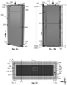
- the component 100 includes a body 110 with a at least one coil 120 defined/fabricated therein by multi-material 3D printing.
- the electric component 100 (and the coil(s) 120 therein) is fabricated by 3D printing of s of at least three different 3D-printable materials M1 to M3 including:
- Fig. 1A illustrates a perspective view of the electric component 100 with the coil 120 therein, and with the bulk material M3 of the body 110 shown/exemplified in translucent color/shade so that the coil 120 therein is visible.
- Fig. 1B illustrates a side view of a part of the coil 120 which is 3D printed within the electric component 100 shown in Fig. 1A , while excluding (not showing) the bulk material M3 of the body 110 of the electric component 100 and also excluding (not showing) the optional flux collectors 126 in order to illustrate the coil 120 with better clarity.
- the coil 120 includes the magnetic channel 129, which includes in this example the core 122 of the coil 120 with two optional magnetic flux collectors 126 arranged from opposite ends thereof.
- the coil 120 also includes an electric channel 128 arranged/configured therein to yield induced voltage through the electric terminals 123 (not specifically shown in Fig. 1A ) of the electric channel 128 in response to magnetic flux propagation through the core 122.
- the magnetic channel 129 and the electric channel 128 may have different shapes.
- at least one of the magnetic 129 and electric 128 channels has coiled/twisted geometry (e.g. a helical or otherwise twisted geometry) and is wrapped/surrounded or otherwise twisted about the other one of the magnetic 129 and electric 128 channels, in order to yield the induced voltage in the electric channel 128 in response to magnetic flux propagation through the core 122 of the magnetic channel 129.
- a magnetic core 122 having a straight/rod-like shape is exemplified in the magnetic channel 129, while the electric channel 128 has conductive windings 124 turned/twisted/coiled such that it form a plurality of turns 124.1 to 124.n wrapped/surrounded about the magnetic core 122 of the magnetic channel 129, so that induced voltage is produced in the electric channel 128 in response to magnetic flux through the core 122 of the magnetic channel 129.
- the magnetic channel 129 and/or the magnetic core 122 thereof are not necessarily shaped to form straight/rod-like core and may be 3D printed with other shapes that are turned/twisted/coiled within the body of the electric component 100.
- the core 122 may be formed with helical, meander-like or coiled shape with the windings 124 surrounding multiple regions thereof.
- Such core shapes may be used in order to facilitate generation of sufficiently high induced voltage of the coil 120 desired sensitivity of the coil 120 to magnetic fields from a desired magnetic field direction/axis F, while with desired dimensional constraints of the coil 120 or of the electric component 100 in its entirety. For instance, in Figs.
- various 3D printed coils 120 are illustrated with their magnetic channels 129 (e.g. magnetic cores 122) having twisted shapes of either a helical, multi/double helical, meander, and/or coiled, shapes; whereby these twisted core shapes facilitate a greater length of the core 122 passing through windings of the electric channel 128 or otherwise surrounding the electric channel 128 thereby increasing the amount of magnetic flux inducing voltage in the electric channel 128 to improve the sensitivity of the coils while facilitating various desired dimensional constraints thereof (to enable fitting them within small medical devices).
- magnetic channels 129 e.g. magnetic cores 122
- twisted shapes of either a helical, multi/double helical, meander, and/or coiled, shapes
- the magnetic channel 129 of the coil 120 includes flux collector(s) 126 magnetically coupled-to the core 122 of the channel 129.
- the flux collector(s) 126 typically a pair of them coupled to opposite sides of the core 122, are configured with respective relatively large facets/surfaces perpendicular to the magnetic axis F of the coil 120 (e.g. typically larger than the cross-section area of the core 122) such that they can collect magnetic flux propagating along the direction of the coil's magnetic axis F, and channel the flux through the core (thereby improving the sensitivity of the coil).
- the flux collectors are optional, and are included in the magnetic channel 129 in some embodiments where the cross-section of the magnetic core 122 is small/narrow and/or when the magnetic core 122 does not extend in direction substantially parallel to the magnetic axis F.
- the electric channel 128 of the coil 120 includes conductive windings 124, including a plurality of turns surrounding the magnetic core 122, in order for voltage to be induced therein in response to magnetic flux through the core 120.
- the conductive windings 124 are optional, as in some implementations, as indicated above, the magnetic core 120 may be itself winded/turned to surround the electric channel 128 such that magnetic flux propagating therein circumferences the electric channel 128 and induces voltage therein.
- the conductive windings 124 may be configured/3D-printed to surround the magnetic core 120 in a coiled shape/path (as illustrated in the example of Fig. 1A ) and/or with spiral shape/path within one or more of the printed layers, and/or with the shape of multiple concentric coils (as illustrated in the example of Figs. 3A to 3I ).
- the electric component 100 of the present invention may include/be-fabricated-with one or with a plurality of coils 120 therein, as well as optionally with other electric circuit elements (not specifically illustrated) such as capacitors and/or resistors and/or electrical connections between them.
- other electric circuit elements such as capacitors and/or resistors and/or electrical connections between them.
- additional 3D printable materials not specifically exemplified herein, such as electrically resistive material for fabrication of resistors, and or material of selected dielectric properties to be 3D printed in between capacitor's conductive plates.
- the electric component 100 of the invention is fabricated utilizing 3D printing method (additive manufacturing technology) that includes a layer-by-layer deposition (and optionally curing), along a printing direction Z, of the at least three printable materials M1 to M3 indicated above.
- 3D printing method additive manufacturing technology
- the at least 3 types of printable materials include: the magnetic material(s) M1, which is used for printing the magnetic channels 129 of the coils 120 (including the magnetic cores 122 and the optional flux collectors 126 thereof); the conductive material(s) M2 which is used for printing the electric channels 128 of the coils (including the conductive windings 124 and the electric contacts/terminals thereof); and non-magnetic electrically insulating (dielectric) material, which is 3D printed to form the bulk of the body 110 of the electric component 100, as well as typically/optionally to fill the spacings between the windings 124 of the coils to electrically insulated between them.
- the magnetic material(s) M1 which is used for printing the magnetic channels 129 of the coils 120 (including the magnetic cores 122 and the optional flux collectors 126 thereof)
- the conductive material(s) M2 which is used for printing the electric channels 128 of the coils (including the conductive windings 124 and the electric contacts/terminals thereof)
- magnetic- material and/or particles is used herein to designate materials of high relative magnetic permeability ⁇ r , for example having relative permeability preferably of ⁇ r ⁇ 100 relative to the vacuum permeability ⁇ 0 , and more preferably in some cases in the order of ⁇ r ⁇ 500, or even in the order of ⁇ r ⁇ 5000.
- non-magnetic-material and or particles are used herein to designate materials of low relative permeability ⁇ r which is substantially lower than that of the magnetic materials used in the electronic components' fabrication and typically in the order of ⁇ r ⁇ 1.
- a flow diagram of a method 200 to fabricate the electric component 100 according to some embodiments of the present invention by multi-material 3D-printing is illustrated.
- the multi-material 3D-printing in this case utilizes at least three different materials M1 to M3 for printing the electric component(s) 100.
- a model of one or more electric component 100 are provided.
- the model may include one or more electric component 100 configured with the principles of the invention as described above with reference to Figs. 1A and 1B and/or as described below with reference to Figs. 3A to 8B .
- the model is indicative 3D spatial distribution (voxel maps) of the at least three materials, M1 to M3, which are to be 3D-printed to fabricate the electric component(s) 100 of the present invention.
- the model is indicative of the respective spatial distributions of the three materials M1 to M3 that should be 3D printed to form an electric component 100 with at least one coil 120 according to the invention.
- the multi-material 3D-printing according to method 200 operates by successive printing of layers, one on top the other, along the printing direction Z (see for instance the layers indicated L 1 , L 2 to L n in Figs. 1B , 3D , 3E , 3H and 3I ).
- the spatial distributions of the three materials M1 to M3 in the model is such that the printing results with one or more electric components 100 each including at least one coil 120 configured according to an embodiment of the present invention.
- a multi-material 3D-printing is applied to print the one or more magnetic field sensors 100 based on the spatial distributions of the three or more materials M1 to M3 in the model.
- the multi-material 3D-printing may be carried out for example by utilizing a photopolymerization 3D-printing technique to print layers L 1 , L 2 to L n that are composed of a combination of several materials having different electromagnetic properties (e.g., two three or optionally more than three materials with different electromagnetic properties may be printed in each layer).
- 3D printing of the electric component 100 described above involves printing of spatial distributions of the at least three materials M1 to M3 having the different electromagnetic properties.
- the electrically conductive material M2 may include for example Silver and/or Copper and/or Palladium, and/or Silver-Palladium alloy.
- the magnetic material M1 may include for example Ceramic-Ferrite material and/or Metal Material.
- the magnetic material M1 is a soft magnetic material having relative permeability ⁇ r of at least 100 or above.
- the magnetic material M1 particularly that used for printing magnetic channel 129 having coiled/twisted or otherwise non-straight shapes, is a material having relative permeability ⁇ r in the order of 500 or above, and even more preferably in the order of 5000 or above, in order to facilitate efficient channeling of magnetic flux through the folds/curves 127 thereof.
- the non-magnetic dielectric (electrically insulating) material M3 (also referred to herein as the bulk material) may for instance include ceramic and/or glass-ceramic.
- the 3D printing of the electric component(s) 100 may be implemented for example based on the principles of Vat Photopolymerization, utilizing for instance stereolithography (SLA) or digital light processing (DLP) for the pattern implementation/projections.
- SLA stereolithography
- DLP digital light processing
- the invention is not limited to these specific technologies and may generally be implemented by other multi-material 3D printing technique as may be developed to be suitable for the fabrication of the electric components according to the invention.
- the electric component(s) 100 with small feature sizes can be printed utilizing 3D printed layers with layer-thicknesses in the scale down to microns (e.g., sintered layer thickness may be about 8-10 microns).
- the pixelated in-layer resolution of the printing may be with pitch/widths of the printed voxels in the order of about 12-25 microns laterally within the layers (i.e. with respect to the lateral coordinates X, Y).
- functional features of the electric component(s) 100 are printed with minimal in-layer feature size ( of at least two voxels, in order to avoid malfunctions of the electric component(s) 100 due to misprints of single/individual voxels. Accordingly, features of the electric component(s) 100 which are printed within a layer may be printed with characteristic in-layer lateral sizes as small as about 24-50 microns or less (this is considering that the lateral pitch/widths of the voxels within the layer is of about 12-25 microns and considering the preference to print each important/functional feature with minimal in-layer feature size of at least two the voxels).
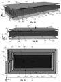
- FIG. 1C showing a cross section of the electric component(s) 100 shown in Fig. 1B along the plane/printed-layer CS marked there, which passes across the winding turn 124.2.
- the turn 124.2 is not closed (opened at region OP) such that it is connected, via conductive vias 121 to other turns of the conductive windings 124 above and below it (in this manner forming the conductive windings 124 in the coil's electric channel 128).
- the term via e.g. referring to elements marked 121 in the figures
- parts/portions of the conductive channel 128 e.g. integral parts thereof
- Fig. 1C shows a pixels' grid PG illustrating the voxel distribution within a certain printed layer of the electric component 100, with P X and P Y marking the voxels' lateral width/pitch along each of the lateral (in-layer) X and Y dimensions (which, as said, may be in the order of 12-25 microns when printing compact electric components).
- the electric channel 128 including the turns of the windings 124 of the coil 120 (which are a functional element thereof) are printed with minimal in-layer feature size of at least two voxels.
- insulation 125 separating parts of the electric channel 128 from other parts thereof (e.g.
- the phrase minimal in-layer feature size is used herein to design the minimal lateral size in voxels/pixels, of a functional feature of the electric component along any lateral (X and/or Y) directions of the 3D-printing within each layer in which it is being printed.
- the term insulation 125 is used herein considering its functional property, to electrically insulate between to conductive features of the electrical component 100, such as between winding turns, and while considering this functional property, any set of voxels of electrically insulative material which are printed within each layer along the shortest path(s) between to conductive features in the layer, should be considered as a part of the insulation 125 between the said conductive features. Accordingly, with this definition, the minimal in layer feature size of the insulation is such that the shortest insulative path(s), in voxels, between conductive features/voxels within a layer extend through at least two voxels of the layer.
- any individual misprint of single voxel in the electric channel 128 will not cause electrical disconnection in the electric channel 128, and any individual misprint of single voxel in the insulation 125 will not affect electric shortcut in the electric channel 128.
- the magnetic channel 129 is printed with the minimal in-layer features size of the at least two voxels (in some implementations it is 3D printed with in-layer features sizes substantially larger than two voxels in order to facilitate efficient propagation of magnetic flux therethrough).
- the turns of the electric channel 128 is printed with in-layer lateral widths W X and/or W Y of at least two voxels along at least one of the lateral dimensions X and Y, and with height of one layer so that they have at least said minimal in-layer feature size of the two voxels. Accordingly, any individual voxel misprint in the winding will not cause electrical disconnection in the electric channel 128 and will not disrupt the operation of the coil 120.
- magnetic material M1 of which the core 122 is made is electrically conductive metal (i.e.
- a magnetic channel 129 printed with a non-ceramic ferrite should be spaced from the electric channel 128, at least at some places, in order to prevent short circuit, which might impact the achievable miniaturization of the magnetic field sensor 100 and/or require more complex design thereof. Therefore, in some embodiments preferably ceramic ferrite material is used for the printing of the magnetic channels 129.
- 3D printing of the magnetic field sensor 100 may be performed layer by layer along a printing direction Z utilizing for example photopolymerization multilateral 3D printing techniques such as SLA or DLP.
- the printing direction Z is typically selected such that it is substantially perpendicular to planes spanned by the turns of the conductive windings 124 of the coils 120.
- the choice of the printing direction Z may have particular importance in the printing of miniature magnetic field sensors 100 because the lateral feature resolution of the printing in the X-Y plane is lower than the "vertical" resolution of the layers obtained along the printing direction Z.
- each layer of the sensor 100 typically includes the following (not necessarily in that order):
- the 3D printing is conducted such that the conductive material M3 of the coils 123 is fully embedded within the bulk of electric component's body 110 in order to protect the conductive material M3 against degradation (e.g. oxidation) due to environmental conditions, particularly during the high temperature sintering 230 which follows layer by layer material deposition and curing.
- degradation e.g. oxidation
- one or more 3D structures of one or more sensors 100 each including at least one longitudinally oriented coil and at least one transversely oriented coil electric coil 220 are obtained.
- Method 200 further includes operation 230 for sintering the one or more 3D structures of the one or more electric components 100 printed in operation 120.
- the sintering is generally performed at temperature sufficient for burning or driving off polymers (binding polymers) from the one or more magnetic field sensors 100 as well as firing ceramic or glass ceramic materials such as M3 and optionally M1 which are used in the printing.
- the material density of the printed ceramic and metal materials (e.g., M1,M2 and M3 ) of the electric components 100 approach 100%.
- the sintering may be performed at temperatures below the Silver melting point (e.g., at temperatures not exceeding 961°C; preferable in this case the sintering temperature may be limited up to about 900C in order to achieve a stable sintering process).
- the sintering may be performed at temperatures below the alloy melting point (the specific melting point depends on the ratio of silver and palladium in the alloy and depending on the composition the melting point is generally between the melting point of silver, 961°C, and that of palladium, 1,555°C).
- the sintering may be performed in an Oxygen deprived environment (so as to avoid oxidation of the Copper), and at temperatures below the 1084°C Copper melting point.
- the method 200 is carried out for 3D-printing electric components 100 in which miniature coils having features of micron scale size are embedded.
- the 3D printed layers may be printed with thicknesses in a range of about 5 to 15 ⁇ m (e.g., 9 ⁇ m), depending on the specific model design and 3D-Printing technology used.
- a pitch of the turns of the windings 124 which may be in the order of twice the pitch of the 3D printed layers, may be within the range of about 10 ⁇ m to 30 ⁇ m along the printing direction Z of the 3D printed layers (e.g., typically turns' pitch of about 18 ⁇ m).
- the method 200 may include operation 240 for separating printed electric components 100 from the building/3D-printing platform (e.g., 201 shown in Fig. 1E).
- the operation 240 may be performed before or after the sintering 230.
- a suitable building platform may be used which can withstand the temperatures of the sintering 230, and the electric components' separation from the platform may be conducted post sintering so as to avoid/reduce damage to the sensors during the separation process.
- method 200 of the present invention provides a novel and inventive technique for fabrication of electric components 100 each including one or more coils 120 as described above.
- the method 200 is suited for fabrication of miniature electric components 100 (with features sizes as small as few microns) that are operable as/in a magnetic-field-based positioning sensors and suited for use in compact/narrow medical devices such as catheters.
- the method 200 may be used in mass production to simultaneously 3D-print large pluralities of miniature such electric components 100 built on the same platform (e.g., typically between hundreds and several thousand electric components 100 may be printed using for instance a vat photopolymerization technology).
- Each electric component 100 may have for example a ceramic/glass-ceramic body 110 embedding therein one or more highly sensitive open magnetic circuit coils 120.
- the coils 120 may be fabricated with small dimensions, for example in the order of ⁇ 0.5 mm to ⁇ 2 mm and may provide high sensitivity/induced-voltage in response to magnetic fields, for example in the range ⁇ 0.1 to 1 ⁇ V/(Gauss*Hz).
- the electronic component 100 includes a magnetic channel 129 and a conductive channel 128 of the coil 120.
- the magnetic channel 129 and conductive 128 channels are 3D printed with magnetic material M1 and electrically conductive material M2 respectively.
- the magnetic channel 129 includes a magnetic core 122 of the coil 120, and the conductive channel 128 includes an arrangement of conductive windings 124 with a plurality of turns surrounding the magnetic core 122 (e.g. some of the turns are individually marked with reference numerals 124.1 to 124.6 in the figures).
- the body/bulk 110 of the electric component 100 is 3D printed with non-magnetic electrically insulating material M3.
- the electrical insulation 125 between the turns of the windings 124 is in this example 3D printed with the same non-magnetic electrically insulating material M3 used for printing the bulk of the body 110.
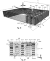
- Fig. 3A shows a perspective view of the complete electric component 100
- Fig. 3B is a side view of the coil 120 within the electric component 100 in which the non-magnetic electrically insulating material M3 is not illustrated for clarity of the figure
- Fig. 3C shows a top view of the coil 120 within the electric component 100, with the flux collectors 126 omitted/not-shown for clarity
- Fig. 3D shows a top view of the coil 120 without showing the electric terminals 123 and showing a pixel/voxel grid PG illustrating the distribution voxel of the 3D printing as captured from the top side of the coil 120
- Fig. 3A shows a perspective view of the complete electric component 100
- Fig. 3B is a side view of the coil 120 within the electric component 100 in which the non-magnetic electrically insulating material M3 is not illustrated for clarity of the figure
- Fig. 3C shows a top view of the coil 120 within the electric component 100, with the flux collectors 126
- FIG. 3E illustrates a cross-section of the windings 124 of the coil 120 with the insulation 125 between them across lateral sides B and D of the coil 120 (in which no conductive vias 121 between turns are accommodated), taken along the cross-section plane CP shown in Fig. 3D ;
- Figs. 3F and 3G illustrate section cuts taken along the respective section planes SP1 and SP2 of the coil 120 shown in Fig. 3E , showing the windings 124 with the insulation 125 between them respectively across the lateral side A (in which the conductive vias 121 between turns in different layers are accommodated) and across the lateral side C of the coil 120 (in which now conductive vias 121 are accommodated); and Figs.
- 3H and 3I are two respective side views showing some of the turns of the conductive windings 124 (without showing the insulation 125 between them), which are taken respectively from lateral side A of the coil 120 along which conductive vias are accommodated between the windings 124 and from lateral side C of the coil 120 along which conductive vias are not accommodated in this example.
- axes indicating the longitudinal direction Z (being the layer-by-layer-printing direction of the electric component 100) and the lateral directions X and Y perpendicular thereto are illustrated.
- guide lines illustrating the 3D printed layers L 1 to L n of the electric component 100, the lateral side A, B, C and D thereof, and the magnetic axis F of the coil 120 therein are illustrated in the figures.
- the via 121.5-6 is printed in layer L n-2 to connect between the turns 124.5 and 124.6 which are 3D printed in the layers above and below it, L n-1 and L n-3 , respectively.
- functional features of the 3D printed electric component(s) 100 are 3D printed with minimal in-layer feature size of at least two voxels.
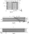
- a configuration of the coil's 120 windings 124 which facilitates compact arrangement of large number of windings' turns, while maintaining a minimal in-layer feature size of at least two voxels in the windings' turns 124 and in the electric insulation 125 between them, is illustrated.
- This configuration thus facilitates the reliable 3D printing of highly sensitive and compact coil(s) in the electric component, since on the one hand any individual voxel misprint in the electric channel 128 or the insulation will not disrupt proper operation of the coil, while on the other hand it provides for stacking large number of windings' turns 124 surrounding the magnetic core 122 thereby facilitating the high sensitivity of the coil 120.
- Figs. 3F and 3G illustrate respective section cut SP1 of the windings 124 across the respective lateral sides A and B thereof in which the conductive vias 121 are respectively accommodated and not accommodated. As shown in Fig.
- the insulation between the adjacent turns within the same layer has a lateral width greater than the minimal in-layer feature size, in this example a widths of four voxels along the side(s) at which no vias are accommodated . As shown in Fig.
- the insulation between the adjacent turns within the same layer along these sides has also a lateral width greater than the minimal in-layer feature size, in this example a widths of six voxels along the side(s) A at which the vias are accommodated.
- the minimal in-layer feature size of the insulation in the spacing/insulation such as 125.6-V between the adjacent turn such as 124.4 and 124.6 within the same layer would have been of only one voxel (e.g. due to the presence there of the via between them (e.g. the via indicated V in the figure which connects between neighboring turns above one another), and would thereby not satisfy the minimal in-layer feature size condition for the insulation 125.
- conductive vias 121 which connect between neighboring turns above or below one another are arranged along as few lateral sides as possible whereby the lateral spacing between concentrically adjacent turns along these sides is of at least two voxels, thereby permitting the lateral spacing between the concentrically adjacent turns along other lateral sides to be of only one voxel to yield one the one hand a compact arrangement of the turns and on the other hand electrical insulation with minimal in-layer feature size of at least to voxels facilitating reliability of the coil's fabrication.
- the electric component 100 is 3D printed by successive printing of a plurality of printed layers L 1 , L 2 to L n along the printing direction Z.
- Each of the turns, e.g. 124.1 to 124.6, of the conductive windings 124 is arranged/3D-printed planarly within one of the printed layers L 1 to L n .
- the turns 124.1, 124.3, and 124.5 are 3D printed planarly within layer L n
- the turns 124.2, 124.4 are 3D printed planarly within layer L n-1 .
- the turns are printed in the multitude of the printed layers.
- the magnetic core is printed such that passes through a consecutive multitude of the printed layers L 1 to L n and surrounded by the turns thereat.
- the electric component 100 i.e. the coil 120 thereof, includes electrical insulation 125 that is 3D printed between the turns of the conductive windings 124.
- the electrical insulation 125 is 3D printed with the same bulk material M3 which is also used to print the body 110 of the electric component 100.
- the turns (e.g., 124.1 to 124.6) of the conductive windings 124 and the insulation material 125 between them (as well as the magnetic channel 129) are 3D printed with minimal in-layer feature size of at least two voxels of the 3D printing.
- the windings 124 includes concentrically adjacent turns that are 3D printed in consecutive layers of the 3D printing with lateral separation of one voxel between the concentrically adjacent turns (at least along some lateral sides of the concentric).
- lateral separation of the one voxel between concentrically adjacent turns is from one or more lateral sides of the adjacent concentric turns (in this example from sides B to D), and the conductive vias are 3D printed in at least one other lateral side of the concentric turns (in this example from side A).
- the lateral separation between the concentrically adjacent turns is of at least two voxels, in order to maintain a minimal in-layer feature size of the insulation to be at least two voxels.
- Figs. 4A and 4B illustrating an electric component 100 according to another embodiment of the present invention, which is/includes a coil 120 having a flattened shape with respect to its magnetic axis F or in other words a coil 120 having a low/small aspect ratio between its length L along its magnetic axis F and its width W traverse to its magnetic axis F.
- a coli with such dimensions is referred to herein as a flattened coil.
- the electric component 100 includes: a body/bulk 110 that is 3D printed with non-magnetic electrically insulating material M3; a magnetic channel 129 that is 3D printed in the body 110 with magnetic material M1 and includes a magnetic core 122 of the coil 120; and a conductive channel 128 that is 3D printed in the body 110 with electrically conductive material M2 and includes conductive windings 124 with a plurality of turns surrounding the core 122.
- the and conductive channel 128 is terminated at both ends thereof by electric contacts/terminals 123 (not specifically shown in Fig. 4B).
- Fig. 4A is a perspective view of the electric component 100 and 4B is a side view of the coil electric component 100 in which the bulk material of the body 110 is not shown.
- the required dimensions of the electric component 100 with the coil 120 therein are such that the electric component 100, and/or the coil 120 therein, is flattened with respect to the direction of its magnetic axis F.
- flattened coils, or otherwise coils with such flattened dimensions are in many cases required for medical devices' position sensing, and in particular are used/fitted in elongated and narrow medical devices, such as catheters, whose positions are often sensed by measuring magnetic field in their surroundings (particularly used for sensing the vector components of the magnetic fields which are perpendicular to the elongated body of the medical device/instrument) - see for instance Fig. 9 and its related description below.
- Some aspects of the present invention provide for overcoming this difficulty, and 3D printing flattened coils 120 with sufficient sensitivity.
- This is achieved by 3D printing the magnetic channel 129 such that it includes at least a pair of flux collectors 126 having respective flux collection facets 126F and 126B that are perpendicular to the magnetic axis F of the coil 120.
- the magnetic channel 129 is 3D printed such that it has curved/folded path with curves/folds 127 defining between them one or more sections of the magnetic core 122 of the magnetic channel 129 which extend along the width dimension W of the coil 120 (i.e. traverse to the coil's magnetic axis F).
- the magnetic channel is thereby adapted to collect, via facets 126F and 126B, magnetic flux propagating from the direction of the magnetic axis F and channel the magnetic flux, via curves 127 to propagate along the core section(s) 122 thereof which extends along the longer width dimension W of the flattened coil 120.
- the windings 124 of the conductive channel 128 of the flattened coil 120 include a plurality of turns 124.1 to 124.m that are arranged to surround the core section(s) 122 which extends along the longer width dimension W of the flattened coil 120.
- the number of turns 124.1 to 124.m that can be arranged in this manner is larger than the number of turns that could be arranged in case the core 122 was to extend in the direction along the magnetic axis F (i.e. along the shorted longitudinal dimension L of the coil 120) and accordingly improved sensitivity of the coil to magnetic field components from the magnetic axis F is obtained, despite the flattened shape of the coil 120 in this embodiment.
- the flux collection facets/surfaces 126F and 126B that face the magnetic axis F of the coil 120 are made wider (e.g. with substantially larger area) than the characteristic width (e.g. cross section area) of the magnetic channel 129 between them.
- the areas of the flux collectors facets/surfaces 126F and 126B are preferably made substantially larger than the characteristic cross section area of the magnetic core section(s) 122 which are facing a different, e.g. perpendicular, direction to the magnetic axis F.
- the flux collectors 126 This is in other in order for the flux collectors 126 to collect much more magnetic field flux from the direction of the magnetic axis F than the amount of flux that would be collected to the magnetic channel 129 from other directions, thus making flattened coil with the turned/folded magnetic channel 129 sensitive to magnetic field components directed along the magnetic axis F, while negligibly sensitive to magnetic field components from other directions.
- the flux collectors 126 and/or other sections of the magnetic channel are also tapered towards the magnetic core sections 122 (e.g. to facilitate efficient flux channeling from the relatively wide flux collection facets/surfaces 126F and 126B thereof to the narrower magnetic core 122).
- the 3D printing technology used for the electric component's 100 fabrication provides for printing layers with thicknesses that are substantially smaller than the lateral widths of the printed voxels (in other words: the layer resolution is substantially higher than the resolution of in-layer pixels that can be 3D printed).
- the thicknesses of the printed layers are of about 8-10 ⁇ m (along the Z direction; typically 9 ⁇ m) while the lateral sizes/widths of the printed voxels within the layers are of about 12-25 ⁇ m. Therefore, in such embodiments, 3D printing the turns 124.1 to 124.m of the windings 124 with planar orientation in the printed layers facilitates printing of thinner turns (e.g.
- the direction Z of printing of the flattened coil 120 and/or the electric component 100 in which it may be contained is chosen/set such that the turns 124.1 to 124.m are printed planarly within the printed layers L 1 to L n (for instance the printing direction Z of the flattened coil 120 may be set parallel to the longer width W dimension of the flattened coil 120 as illustrated in the figures).
- This facilitates printing a stack of further more number of turns 124.1 to 124.m surrounding the core section 122 (with higher density of turns) and thus further improving the sensitivity of the coil 120.
- functional features of the flattened coil 120 may be 3D printed with minimal in-layer feature size of at least two voxels of the 3D printing in order to facilitate reliable 3D printing of the coil 120 that is robust to misprints of individual voxels. This may be in like manner as described above with reference to Figs. 1A to 1C .
- the turns 124.1 to 124.m of the windings may optionally include pluralities of concentric turns (not specifically shown), in order to further increase the count of turns surrounding the magnetic core 122, and thus improve the coil's sensitivity.
- the spacings/insulation 125 between concentric turns may optionally be configured in like manner as described with reference to the embodiment of Figs. 3A to 3I .
- Figs. 4A and 4B one optional configuration of the 3D printed flattened coil 120 (and/or of an electric component 100 containing the same) is exemplified.
- the magnetic channel 129 of that flattened coil 120 being curved/folded 127 such that one or more sections of the magnetic channel 129 extends substantially along the longer width dimension W of the flattened coil (perpendicular to its magnetic axis F) printing direction to serve as the magnetic core 122 of the coil and is being surrounded by conductive turns of the windings 124.
- FIGS. 5A to 8B provide self-explanatory depictions of several other non-limiting examples of configurations of coils 120 whose magnetic channels 129 are curved/folded in order to facilitate configurations of windings to have a plurality of magnetic core sections 122 facilitating an arrangement of the winding turns and/or increasing their number improving the coils sensitivity.
- Like reference numerals are used in Figs. 5A to 8B to designate elements/sections of similar functionality as in the coils described above with reference to Figs. 1A to 1C and 3A to 4B.
- Figs. 5A to 5D respectively exemplify, in self-explanatory manner, perspective-side-, front- and back- views of an electric component, in this example including a coil 120, which may be 3D printed according to embodiments of the present invention.
- the magnetic channel 129 is curved/folded 127 several times such that between the flux collectors 126, the magnetic channel 129 is printed-with/has a helical-like shape with a plurality of magnetic core section 122 thereof extending substantially along the printing direction Z.
- the plurality of core sections 122 are surrounded by turns of the conductive windings 124 of the conductive channel, which are planarly printed in the 3D printed layers, with relatively small pitch/distances between them.
- the turns of the conductive windings 124 are typically spaced from one another by electrical insulation printed in the layers between them (e.g. the electrical insulation may be printed with between the turns with the bulk material M3).
- the magnetic channel 129 is formed in a helical like shape, such that the multiple magnetic core sections 122 thereof traverse through the conductive windings 124 to channel magnetic flux, which flows between the flux collectors 126 along the magnetic channel 129, to pass several times through the conductive windings 124 and thereby provide improved sensitivity of the coil 120.
- the magnetic channel 129 is folded such that two magnetic core sections 122 thereof traverses through the windings 124, it should be appreciated by those versed in the art that the coil 120 may generally be printed with other configurations of the helical channel and may be formed with any suitable number of folds 127 to yield any suitable number of magnetic core sections through the windings that provide the optimized sensitivity for the specific sensory application for which it is used.
- Figs. 6A and 6C respectively exemplify, in self-explanatory manner, side- and front views of a coil 120 with a plurality of helical magnetic sub-channels, 129.1 and 129.2, which may be printed in the electric components 100 according to embodiments of the present invention.
- Fig. 6A and 6C respectively exemplify, in self-explanatory manner, side- and front views of a coil 120 with a plurality of helical magnetic sub-channels, 129.1 and 129.2, which may be printed in the electric components 100 according to embodiments of the present invention.
- Fig. 6A and 6C respectively exemplify, in self-explanatory manner, side- and front views of a coil 120 with a plurality of helical magnetic sub-channels, 129.1 and 129.2, which may be printed in the electric components 100 according to embodiments of the present invention.
- Fig. 6A and 6C respectively exemplify, in self-explanatory manner
- FIG. 6C is a perspective view of the helical magnetic sub-channels
- the magnetic channel 129 is split into a plurality of magnetic subchannels (two in this example 129.1 and 129.2) each being curved/folded 127 several times in the form of a helix (or otherwise a helical-like shape), such that the magnetic channel 129 has a multi-helix shape (double helix in this example - one helix formed by each of the magnetic subchannel 129.1 and 129.2).
- the magnetic sub-channels 129.1 and 129.2 are printed with curves/folds 127 such that they define a plurality of magnetic core sections 122 extending substantially along to the printing direction Z and are surrounded by turns of the conductive windings 124 of the coil 120.
- the conductive windings 124 include several winding sets 128A to 128D each including a plurality of conductive turns surrounding different one or more of the magnetic core sections 122.
- the electric channel 128 between the electric contacts/terminals thereof may be 3D printed as a single conductive path passing between the pair of electric contacts/terminals and shaped to form the winding sets 128A to 128D along a single conductive path, or the electric channel 128 between the electric contacts may be printed to split into several (e.g. 4) electric sub channels (e.g. which may be connected to one another near the electric contacts in parallel) and each forming a plurality of windings/turns of the one or more winding sets 128A to 128D.
- the magnetic channel 129 has a tapered shape/structure in a region thereof between the flux collection surfaces/facets of the flux collectors 126 and the magnetic core sections 122.
- the example illustrated in Figs. 6A to 6C exemplifies such tapered shape of the magnetic channel 129 in which the cross-section area/width of the magnetic channel 129 is getting narrower along the direction advancing from the flax collectors 126 towards the core sections 122 of the channel.
- the tapering of the magnetic channel 129 is made gradually at several location including tapering of the flux collectors 126, as shown in the tapered regions 129A marked in Fig.
- tapering of the section 129B of the magnetic channel 129 that directs the magnetic flux between the flux collectors 126 to the core sections 122 as illustrated in Fig. 6C .
- the tapering provides for improved coupling of external magnetic flux propagating collected by the flux collectors 126 to flow through the magnetic channel 126, and thereby improves the sensitivity of the coil 120.
- the tapering of the magnetic channel towards the magnetic core thereof may also be implemented in other embodiments of the present invention, for example in coils 120 with configurations such as exemplified in Figs. 1A to 1C , 3A to 5D described above and/or in Figs. 7A to 8B described below.
- Figs. 7A and 7B exemplify, in self-explanatory manner, a yet another example of an electric component including a coil 120, which may be 3D according to the present invention.
- Fig. 7A depicts a perspective view of the coil 120 and
- Fig. 7B depicts a cross-sectional view of the coil 120 taken along the plane CP illustrated in Fig. 7A .
- the magnetic channel 129 extends between the flux collectors 126 in a meander-like shape/path.
- the flux collectors 126 are not shown in Fig. 7B , yet instead one of the regions 126X of the magnetic channel 129 is shown to which one of the flux collectors 126 is coupled.
- Figs. 7A depicts a perspective view of the coil 120
- Fig. 7B depicts a cross-sectional view of the coil 120 taken along the plane CP illustrated in Fig. 7A .
- the magnetic channel 129 extends between the flux collectors 126 in a meander-like
- the magnetic channel 129 is printed with the curves/folds 127 such that core section(s) 122 thereof (in this case a plurality of core sections) extend substantially along the printing direction Z. Accordingly the magnetic core sections 122 are surrounded by turns of the conductive windings 124 which include a plurality of conductive turns surrounding different one or more of the magnetic core sections 122.
- the electric channel 128, may be printed as a single conductive path passing between two electric contacts/terminals (not specifically shown) at opposite ends thereof, and shaped to form the winding sets 128A to 128D along a single conductive path, or the electric channel 128 between the electric contacts may be printed to split into several (e.g. 4) electric sub channels forming winding sets 128A to 128D which may be electrically connected to one another (e.g. in series in order to increase the output voltage of the coil).
- the 3D printed coils 120 with the meander-like and/or helical-like magnetic channels 129 may be advantageous in some cases in terms of their sensitivity. This is due to the shapes of their magnetic channel which facilitates packing longer total core sections 122 and thus higher count of windings' 124 turns surrounding them, within electric components/coils 120 having compact dimensions.
- coils 120 with the meander-like and/or helical-like magnetic channels 129 are suited for forming flattened coils similar to that illustrated in the embodiment of Figs. 4A and 4B , and the features of the flattened coil 120 exemplified in Figs.
- windings 124, and/or the winding sets 128A to 128D in the embodiments of Figs. 5A to 7B may in some embodiments be implemented with concentric winding configuration including a plurality of concentrically arranged turn stacks similar to the windings 124 illustrated in Figs. 3A to 3I , in order to yield improved sensitivity of the coil 120.
- the lateral spacing between concentrically arranged turns may be of only one voxel in a manner similar to that described with reference to Figs. 3A to 3I , in order to facilitate more compact packing of higher count of turns within compact dimensions thus further improving the coil's sensitivity.
- FIG. 8A and 8B illustrated is a 3D printed coil 120 (e.g. or of an electric component containing it) according to an embodiment of the invention, in which the magnetic channel 129 is curved/folded to follow/form a coiled-like path/shape (e.g. such that it is wrapped about the conductive windings 124 of the coil 120).
- Fig. 8A depicts a perspective view of the coil 120 including the flux collectors 126
- Fig. 5B depicts another perspective view of the coil 120 without showing the flax collectors 126, so that the internal configuration of the coiled magnetic core 122 and its wrapping about the conductive windings 124 is visible in the figure.
- Like reference numerals are used in Figs. 8A and 8B to designate elements/sections/parts of similar functionality as in the coils of the other embodiments of the invention described above.
- the magnetic flux collected by one of the flux collectors 126 is channeled by the magnetic channel 129 to circumference the conductive turns of the windings 124, typically for a plurality of times.
- magnetic flux collected from the top flux collection surface 126U illustrated in Fig. 8A is channeled through the magnetic channel 129 from the region 126X of the magnetic channel 129 (being the connection between the flux collector to the coiled magnetic core 122) to follow sequentially through coiled sections C1 to C8 of the core 122 and then exit the coil 120 though the bottom flux collection surface 126D.
- the coiled core configuration illustrated in this embodiment is suitable for fabrication of a flattened coil, as described above, whereby the printing direction Z is not necessarily transverse to the magnetic axis F of the coil 120.
- the printing direction Z is substantially parallel to the magnetic axis F.
- the winding turns are preferably 3D printed with planar orientations within the printing layers, as exemplified in these figures, however it should be noted that in other embodiments the winding turns may also be 3D printed in other orientations.
- a coil 120 with similar coiled configuration of the magnetic core 122 may be fabricated such that its magnetic axis F is perpendicular to the printing direction Z, thus optionally implementing a flattened coil configuration similar to that described above with reference to Figs. 4A and 4B but with a coiled configuration of the core 122.
- a flattened coil configuration would be obtained by arranging the flux collectors 126 to be located from the lateral sides A and C of the coil 120 which are marked in Fig. 8B ; or alternatively 3D printing the turns of the conductive windings 124 with orientation perpendicular to the magnetic axis (e.g. parallel to the printing direction, such the turns or some of them are printed across multiple printed layers).
- the conductive windings include plurality of turns 124S stacked along the printing direction Z in a plurality of printing layers (e.g. as indicated above in some embodiments printing the turns with such orientation facilitates the relatively small spacing between the stacked turns due to the layers' thicknesses being substantially smaller than the lateral width of the printed voxels).
- the multiple turns 124C are printed concentrically in order to provide further improved sensitivity of the coil 120.
- the turns of the windings 124 are printed with similar configuration and insulation between them as illustrated in the example of Figs. 3A to 3I to thereby obtain compact packing of a plurality of conductive turns surrounding the core sections C1 to C8, thus yielding highly sensitive coil 120 having compact dimensions.
- the figures described above schematically illustrate various non-limiting examples of 3D printed electric components 100, and/or of 3D printed coils 120.
- the turns of the conductive windings 124 of the coils are 3D printed planarly within the printing layers in order to exploit the smaller pitch between printing layers, which is smaller than lateral dimensions of the printed voxels, for packing/printing a higher count of conductive winding turns in the coils and facilitate high sensitivity of coils (i.e. facilitate high induced voltage in response to magnetic field sensing).
- functional features of the coils/electric-components are 3D printed with minimal in-layer feature size of at least two voxels, in order to yield reliable 3D printing of the coils/electric-components.
- concentric winding turns are packed compactly with lateral spacing of only one voxel between concentrically adjacent turns.
- the invention also provides a technique for fabrication a high sensitivity flattened coil having a low/small aspect ratio between its length along its magnetic axis and its width traverse to its magnetic axis .
- This may be achieved by 3D printing at opposite ends of the magnetic channel 129, a pair of flux collectors 126 facing the magnetic axis F to collect flux propagating therefrom, and further printing the magnetic channel 129 with turn(s)/fold(s)/curve(s) 127 between the pair of flux collectors so that one or more core sections 122 thereof extends along the printing direction Z and passes through the conductive windings 124.
- a highly sensitive flattened coil may also be fabricated by utilizing a coiled core configuration.
- method 200 further includes operation 250 for fabricating/attaching surface mount contacts to the 3D printed electric components 100 or to the coil(s) 120, to facilitate their installation on a circuit board via surface mount technology (SMT).
- SMT surface mount technology
- the SMT contacts/mounts comprise for example chemically/electrochemically deposited Tin-plated Copper or Nickel and are fabricated/attached to the 3D printed electric components 100 /coils 120 and coupled to their electric contacts 123 only after the 3D-printing and Sintering of the components 100 /coils 120 .
- one or more of the coils 120 of the sensor 100 are designed with an open magnetic circuit configuration of their magnetic channel 129 /core 122; that is suitable for accurate sensing of magnetic fields, and in particular suitable for magnetic field bases position sensing in medical applications/devices such as in catheters.
- the phrase open magnetic circuit configuration should be understood herein as relating to coil structures with an open-ended magnetic channel that poses substantially no shielding or shunting of external magnetic fields enabling the external magnetic field pass through the coil's magnetic core.
- the 3D printed magnetic field sensor 100 of the present invention as described above, particularly when printed with the coils 120 having open magnetic circuit configurations, may be suited for use as position and/or force sensors in medical instrument/device requiring the same.
- Fig. 9 illustrating a side-view of a medical instrument 1000 (e.g., probe/catheter) according to an embodiment of the present invention in which a position sensor 300 including 3D printed coils 120 configured according to the present invention, (and/or electric component(s) 100 of the invention including the same).
- a medical instrument 1000 e.g., probe/catheter
- a position sensor 300 including 3D printed coils 120 configured according to the present invention and/or electric component(s) 100 of the invention including the same.
- the medical instrument 1000 includes a housing H with a magnetic field-based position sensor 300 furnished therein.
- the medical instrument's housing H includes a main section M and a tip section T which is coupled at a distal end of the main section M via a banding coupler J (e.g. a spring or joint).
- the banding coupler J is configured such that the orientation of the tip section T can be bent relative to the longitudinal axis LX of the housing H under applied force FC (which may be applied for example when tip section T of the medical instrument 1000 is in contact with a body tissue of a patient) with banding degree corresponding to a magnitude and direction of the applied force FC.
- the position sensor 300 a location and orientation sensor 320, and a force sensor 310, which are implemented by 5 coils 120.1 to 120.5 one or more of which are configured and operable according to the present invention.
- the location and orientation sensor 320 utilizes 3 of the coils, including coils 120.4, 120.5 and at least one of the coils 120.1 to 120.3 for measuring magnetic fields produced by one or more magnetic field sources MF L that are located externally to the instrument 1000, and which produce magnetic fields whose measurements are indicative of the spatial location and orientation of the medical instrument 1000.
- the coils 120.4, 120.5 and the at least one coil of the coils 120.1 to 120.3 are arranged such that their magnetic axes span 3 dimensions to thereby facilitate determining the 3D location and/or orientation of the medical instrument 1000 based on measurements of the magnetic fields form the magnetic field sources MF L by said coils.
- the force sensor 310 utilizes the 3 coils 120.1 to 120.3 in order to determine the relative of orientation between the tip and the main sections, T and M, of the housing H. As indicated above the relative of orientation between the tip and the main sections, T and M, is indicative of the force FC applied by the tip section T, for example on a patient's tissue. To this end the force sensor 310 also includes a magnetic field source MFo that produces a reference magnetic field whose measurement by the coils 120.1 to 120.3 provide indication of the relative orientation between the tip and main sections, T and M.
- MFo magnetic field source
- the coils 120.1 to 120.3 of the orientation sensor 310 and the magnetic field source MFo are arranged in the housing H at different sides of the joint J, so that the measurements of the magnetic field from the magnetic field source MFo by the coils of the orientation sensor 310 provide indication of the relative orientation between the tip and the main sections, T and M.
- the magnetic field source MFo is arranged at the tip section T and the coils 120.1 to 120.3 of the orientation sensor 310 are arranged at the main section M with their magnetic axes parallel to the longitudinal axis LX of the housing H (although opposite arrangement may also be applicable).
- the coils 120.1 to 120.3 are generally arranged such that their magnetic axes are collinear to one another (while not being co-planar in order to facilitate the relative orientation to be measured with respect to two angles, e.g. indicative of the pitch and yaw of the tip T relative to the main section).
- the magnetic-field based position sensor 300 of the medical device 1000 is implemented with one or more of the coils 120.1 to 120.5 being a 3D printed open magnetic circuit coils, which are configured according the present invention and/or fabricated by the 3D printing method described above.
- the housing has a narrow width/diameter of about 2 mm, and accordingly the coils 120.1 to 120.5 are compact coils extending typically no more than 0.5 mm in the radial direction with respect to the longitudinal axis of the medical instrument.
- the two coils 120.4 and 120.5 are also 3D printed coils according to the present invention, with SMT mounts fabricated/coupled thereto according to the optional method operation 250 described above. These coils 120.4 and 120.5 are furnished on a flexible circuit board CB which is folded/rolled to a cylindrical shape within the housing H of the medical instrument 1000, such that their magnetic axes are substantially not parallel to one another and also not parallel (typically perpendicular) to the longitudinal axis LX of the housing H.
- the two coils 120.4 and 120.5 are preferably similar coils having flattened geometry, and may optionally be configured according to any one of the embodiments of Figs. 4A to 8B , which facilitate 3D printing of flattened coils with sufficient sensitivity for use in medical device position sensors.
- the conductive windings of any one or more of the coils 120.1 to 120.5 may also be implemented/configured according to the techniques described above with reference to Figs. 3A to 3I to yield densely packed winding turns, and thereby improved sensitivity of the coils with compact dimensions.
- the coils are fabricated such that their functional features are printed with minimal in-layer feature size of at least to voxels of the 3D printing, as described above with reference to Figs. 1A to 1C .
- coils 120.1 to 120.5 used in the position sensor 300 are 3D printed coils of the present invention, in other embodiments of the invention some of the coils 120.1 to 120.5 are not necessarily be 3D printed coils, for instance coils 120.4 and 120.5 may be conventional wire winded coils, without departing from the invention.
- coils 120.1 to 120.3 are printed within a single electric component 100 and coils 120.4 and 120.5 are individually 3D printed coils furnished on a circuit board (in this non-limiting example furnished with SMT technology), in other embodiments of the present invention any number or combination of the coils 120.1 to 120.5 may be either 3D printed as individual coils and/or 3D printed as parts of one or more electric components containing them which are 3D printed according to the invention. For instance, in some implementations all the 5 coils may be part of a single 3D printed electric component according to the invention.
- 3D printing of electric components and coils of the present invention facilitates reliable, accurate and cost-effective fabrication of open and fitting of open magnetic circuit coils within the narrow dimensions of small medical devices while facilitating sufficient sensitivity of the coils for serving as accurate position sensors of such medical device.
- Example 2 The method according to Example 1, wherein the 3D printing includes successive printing of a plurality of printed layers along a printing direction; and wherein the turns of the conductive windings are 3D printed planarly within the printed layers and are 3D printed in the multitude of the printed layers; and wherein the magnetic core passes through a consecutive multitude of the printed layers.
- Example 3 The method according to Example 2, wherein at least some of the turns are 3D printed in consecutive layers.
- Example 5 The method according to Example 4, wherein the turns of the conductive windings include adjacent concentric turns that are 3D-printed in consecutive layers of the 3D printed layers with lateral separation of one voxel between them (i.e. between the adjacent concentric turns).
- Example 6 The method according to Example 5, wherein the lateral separation of the single voxel between adjacent concentric turns is arranged with respect to one or more lateral sides of the adjacent concentric turns, and the conductive vias are arranged along at least one other lateral side of the concentric turns; and wherein the lateral separation between the adjacent concentric turns along the at least one other lateral side is of at least two voxels in order to maintain electrical insulation with the minimal in-layer feature size of the at least two voxels along that at least one other lateral side.
- Example 7 The method according to Example 6, wherein the turns include neighboring concentric turns 3D printed within the same layer and at least one adjacent concentric turn printed in a consecutive layer above or below the said same layer; and wherein a lateral separation between the neighboring concentric turns within the said same layer is of four voxels along the one or more lateral sides, and of six voxels along the at least one other lateral side; thereby facilitating the minimal in-layer feature size of the electrical insulation between each of the neighboring concentric turns and the at least one adjacent concentric turn.
- Example 8 The method according to any one of Examples 1 to 7, wherein the magnetic channel is configured with an open magnetic circuit configuration, and the 3D printing of the magnetic channel includes printing a pair of flux collectors at opposite ends of the magnetic core having respective flux collection facets defining a magnetic axis of the coil between them.
- Example 9 The method according to Example 8, wherein the flux collection facets of the flux collectors are wider than the magnetic core.
- Example 10 The method according to Example 8 or 9, wherein the flux collectors are tapered with the narrower facets of their tapering connected at respective opposite ends of the magnetic core and their wider facets serving as the flux collection facets.
- Example 11 The method according to any one of Examples 1 to 10, wherein the magnetic core has a rod-like shape.
- Example 12 The method according to any one of Examples 8 to 11, wherein the coil is a flattened coil having a small/low aspect ratio between its length along its magnetic axis and its width traverse to its magnetic axis; and wherein the magnetic channel is 3D printed along a curved (e.g. folded) path such that one or more sections of the magnetic core extend along a transvers direction with respect to the magnetic axis of the coils with a length of the one or more sections (e.g.
- Example 13 The method according to Example 12, wherein the curved path of the magnetic channel is such that the magnetic core has a straight, rod-like shape, extending along the transvers direction with respect to the magnetic axis.
- Example 16 The method according to any one of Examples 1 to 15, wherein the method includes 3D printing a body of the electric component with non-magnetic electrically insulating material, at regions not occupied by the magnetic and conductive channels; and wherein the conductive material of the conductive channel is fully embedded within the body so as to be isolated from environmental conditions by which it might be degraded.
- Example 19 An electric component fabricated by the method of any one of Examples 1 to 18.
- Example 20 A flattened coil having small/low aspect ratio between its length along its magnetic axis and its width traverse to its magnetic axis; the coil includes:
- Example 21 An electronic component including at least one coil; the electronic component includes:
- Example 23 The electronic component according to Example 22, wherein the electronic component includes electrical insulation 3D-printed between adjacent turns of the conductive windings with minimal in-layer feature size of the electrical insulation of at least two voxels of 3D-printed electrically insulating material; and the conductive channel includes conductive vias that electrically connect between turns in different layers.
- Example 24 The electronic component according to Example 23, wherein the turns include concentrically adjacent turns 3D-printed in consecutive layers of the 3D printed layers, with lateral separation of one/single voxel between them (i.e. between the concentrically adjacent turns).
- Example 25 The electronic component according to Example 24, wherein the lateral separation of the one/single voxel between concentrically adjacent turns is from one or more lateral sides of the adjacent concentric turns, and wherein the conductive vias are 3D-printed along at least one other lateral side of the concentric turns; and wherein the lateral separation between the adjacent concentric turns along the at least one other lateral side is of at least two voxels in order to maintain the minimal in-layer feature size of the insulation such that it is of at least two voxels along that at least one other lateral side.
- Example 26 A method to fabricate a coil device having small/low aspect ratio between its length along its magnetic axis and its width traverse to its magnetic axis;
- Example 27 A coil device fabricated by the method of Example 26.
- Example 28 A method to fabricate a coil device, the method includes:
- Example 29 The method according to Example 28, wherein the lateral separation of the one/single voxel is 3D-printed relative to one or more lateral sides of the concentrically adj acent turns; wherein the 3D-printing of the conductive channel includes 3D printing of conductive vias along at least one other lateral side of the turns for electrically connecting between turns in different layers; and wherein the lateral separation between the adjacent concentric turns along the at least one other lateral side is of at least two voxels in order to maintain electrical insulation between the turns with minimal in-layer feature size at least two voxels along the at least one other lateral side.
- Example 30 A coil device fabricated by the method of Examples 28 or 29.
Landscapes
- Engineering & Computer Science (AREA)
- Power Engineering (AREA)
- Health & Medical Sciences (AREA)
- Manufacturing & Machinery (AREA)
- Life Sciences & Earth Sciences (AREA)
- Physics & Mathematics (AREA)
- Chemical & Material Sciences (AREA)
- Materials Engineering (AREA)
- Public Health (AREA)
- Biophysics (AREA)
- Heart & Thoracic Surgery (AREA)
- Veterinary Medicine (AREA)
- Biomedical Technology (AREA)
- Animal Behavior & Ethology (AREA)
- General Health & Medical Sciences (AREA)
- General Physics & Mathematics (AREA)
- Surgery (AREA)
- Molecular Biology (AREA)
- Pathology (AREA)
- Medical Informatics (AREA)
- Condensed Matter Physics & Semiconductors (AREA)
- Human Computer Interaction (AREA)
- Mechanical Engineering (AREA)
- Structural Engineering (AREA)
- Composite Materials (AREA)
- Microelectronics & Electronic Packaging (AREA)
- Civil Engineering (AREA)
- Ceramic Engineering (AREA)
- Anesthesiology (AREA)
- Pulmonology (AREA)
- Hematology (AREA)
- Optics & Photonics (AREA)
- Coils Or Transformers For Communication (AREA)
- Measuring Magnetic Variables (AREA)
- Media Introduction/Drainage Providing Device (AREA)
- Coils Of Transformers For General Uses (AREA)
- Manufacturing Cores, Coils, And Magnets (AREA)
Applications Claiming Priority (1)
| Application Number | Priority Date | Filing Date | Title |
|---|---|---|---|
| US202363533258P | 2023-08-17 | 2023-08-17 |
Publications (3)
| Publication Number | Publication Date |
|---|---|
| EP4521429A2 true EP4521429A2 (de) | 2025-03-12 |
| EP4521429A3 EP4521429A3 (de) | 2025-05-07 |
| EP4521429B1 EP4521429B1 (de) | 2026-02-18 |
Family
ID=92458200
Family Applications (3)
| Application Number | Title | Priority Date | Filing Date |
|---|---|---|---|
| EP24194931.2A Active EP4510154B1 (de) | 2023-08-17 | 2024-08-16 | System und verfahren zur erfassung der position und kraft eines katheters |
| EP24194946.0A Pending EP4510155A1 (de) | 2023-08-17 | 2024-08-16 | Magnetfeldsensor |
| EP24194993.2A Active EP4521429B1 (de) | 2023-08-17 | 2024-08-16 | Elektrische komponenten mit spulen und verfahren zur herstellung davon durch 3d-drucken |
Family Applications Before (2)
| Application Number | Title | Priority Date | Filing Date |
|---|---|---|---|
| EP24194931.2A Active EP4510154B1 (de) | 2023-08-17 | 2024-08-16 | System und verfahren zur erfassung der position und kraft eines katheters |
| EP24194946.0A Pending EP4510155A1 (de) | 2023-08-17 | 2024-08-16 | Magnetfeldsensor |
Country Status (5)
| Country | Link |
|---|---|
| US (3) | US20250057438A1 (de) |
| EP (3) | EP4510154B1 (de) |
| JP (3) | JP2025028039A (de) |
| CN (3) | CN119492316A (de) |
| IL (3) | IL315070A (de) |
Families Citing this family (1)
| Publication number | Priority date | Publication date | Assignee | Title |
|---|---|---|---|---|
| US20250009247A1 (en) * | 2023-06-27 | 2025-01-09 | Biosense Webster (Israel) Ltd. | System and method of sensing catheters location and force |
Citations (2)
| Publication number | Priority date | Publication date | Assignee | Title |
|---|---|---|---|---|
| US1569320A (en) | 1925-02-20 | 1926-01-12 | Maurice F Griffin | Trunk |
| US8535308B2 (en) | 2007-10-08 | 2013-09-17 | Biosense Webster (Israel), Ltd. | High-sensitivity pressure-sensing probe |
Family Cites Families (5)
| Publication number | Priority date | Publication date | Assignee | Title |
|---|---|---|---|---|
| DE102012220022B4 (de) * | 2012-11-02 | 2014-09-25 | Festo Ag & Co. Kg | Verfahren zur Herstellung einer Spule und elektronisches Gerät |
| EP3053190B1 (de) * | 2014-12-09 | 2021-05-26 | Google LLC | Verfahren zur herstellung einer dreidimensionalen horizontalen spulenstruktur in einer gussmasse mit mindestens einem integrierten schaltungsbauteil |
| CN105632893B (zh) * | 2015-12-23 | 2018-08-10 | 清华大学 | 基于3d打印制备微电感的方法 |
| US11779239B2 (en) * | 2016-09-01 | 2023-10-10 | St. Jude Medical International Holding S.À R.L. | Core designs for miniature inductive coil sensors |
| US11672461B2 (en) * | 2018-07-16 | 2023-06-13 | Biosense Webster (Israel) Ltd. | Flexible circuit with location and force-sensor coils |
-
2024
- 2024-08-16 US US18/807,145 patent/US20250057438A1/en active Pending
- 2024-08-16 US US18/807,192 patent/US20250062068A1/en active Pending
- 2024-08-16 JP JP2024136500A patent/JP2025028039A/ja active Pending
- 2024-08-16 EP EP24194931.2A patent/EP4510154B1/de active Active
- 2024-08-16 JP JP2024136806A patent/JP2025028040A/ja active Pending
- 2024-08-16 US US18/807,162 patent/US20250057440A1/en active Pending
- 2024-08-16 JP JP2024136967A patent/JP2025028041A/ja active Pending
- 2024-08-16 EP EP24194946.0A patent/EP4510155A1/de active Pending
- 2024-08-16 EP EP24194993.2A patent/EP4521429B1/de active Active
- 2024-08-18 IL IL315070A patent/IL315070A/en unknown
- 2024-08-18 IL IL315068A patent/IL315068A/en unknown
- 2024-08-18 IL IL315067A patent/IL315067A/en unknown
- 2024-08-19 CN CN202411136553.XA patent/CN119492316A/zh active Pending
- 2024-08-21 CN CN202411151054.8A patent/CN119489550A/zh active Pending
- 2024-08-21 CN CN202411149219.8A patent/CN119493053A/zh active Pending
Patent Citations (2)
| Publication number | Priority date | Publication date | Assignee | Title |
|---|---|---|---|---|
| US1569320A (en) | 1925-02-20 | 1926-01-12 | Maurice F Griffin | Trunk |
| US8535308B2 (en) | 2007-10-08 | 2013-09-17 | Biosense Webster (Israel), Ltd. | High-sensitivity pressure-sensing probe |
Also Published As
| Publication number | Publication date |
|---|---|
| EP4510154C0 (de) | 2026-01-28 |
| US20250057440A1 (en) | 2025-02-20 |
| EP4521429B1 (de) | 2026-02-18 |
| US20250062068A1 (en) | 2025-02-20 |
| JP2025028041A (ja) | 2025-02-28 |
| EP4521429A3 (de) | 2025-05-07 |
| CN119489550A (zh) | 2025-02-21 |
| CN119492316A (zh) | 2025-02-21 |
| JP2025028040A (ja) | 2025-02-28 |
| EP4510154B1 (de) | 2026-01-28 |
| EP4510155A1 (de) | 2025-02-19 |
| EP4510154A1 (de) | 2025-02-19 |
| CN119493053A (zh) | 2025-02-21 |
| IL315070A (en) | 2025-03-01 |
| IL315067A (en) | 2025-03-01 |
| IL315068A (en) | 2025-03-01 |
| US20250057438A1 (en) | 2025-02-20 |
| JP2025028039A (ja) | 2025-02-28 |
Similar Documents
| Publication | Publication Date | Title |
|---|---|---|
| EP2214181B1 (de) | Geschichtete elektronische komponente und elektronisches komponentenmodul damit | |
| EP0134556B1 (de) | Scheinwiderstandselement | |
| CN108417361B (zh) | 线圈装置 | |
| EP1271572A1 (de) | Rauschfilter und elektronisches gerät mit rauschfilter | |
| EP4521429A2 (de) | Elektrische komponenten mit spulen und verfahren zur herstellung davon durch 3d-drucken | |
| EP0460506A2 (de) | Elektrische Spulenanordnung zur Verwendung als Transformator oder dergleichen | |
| GB2102632A (en) | Electronic components e.g. inductors | |
| CN104078196B (zh) | 具有热稳定电阻的电感器 | |
| CN109585122A (zh) | 磁耦合型线圈部件 | |
| CN107527721A (zh) | 共模扼流线圈 | |
| CN103578703A (zh) | 芯片装置、多层芯片装置及其制造方法 | |
| EP4483799A1 (de) | System und verfahren zur erfassung der position und kraft eines katheters | |
| CN113396462A (zh) | 线圈和用于制造线圈的方法 | |
| US6255933B1 (en) | Inductance device and manufacturing method thereof | |
| US4581598A (en) | Segmented toroidal air-core transformer | |
| CN114974801B (zh) | 层叠线圈部件 | |
| KR101629890B1 (ko) | 코일 부품 및 이를 포함하는 전원공급장치 | |
| KR102827666B1 (ko) | 코일 부품 | |
| KR20230143842A (ko) | 코일 부품 | |
| JPH07320936A (ja) | 積層形チップインダクタ | |
| JP3476887B2 (ja) | コイル部品および電極の形成方法 | |
| JP2005085968A (ja) | 巻線型インダクタ及びその製造方法 | |
| KR20260027777A (ko) | 코일 부품 | |
| JP3214661B2 (ja) | 電磁流量計 | |
| CA1253587A (en) | Segmented toroidal air-core transformer |
Legal Events
| Date | Code | Title | Description |
|---|---|---|---|
| PUAI | Public reference made under article 153(3) epc to a published international application that has entered the european phase |
Free format text: ORIGINAL CODE: 0009012 |
|
| STAA | Information on the status of an ep patent application or granted ep patent |
Free format text: STATUS: THE APPLICATION HAS BEEN PUBLISHED |
|
| AK | Designated contracting states |
Kind code of ref document: A2 Designated state(s): AL AT BE BG CH CY CZ DE DK EE ES FI FR GB GR HR HU IE IS IT LI LT LU LV MC ME MK MT NL NO PL PT RO RS SE SI SK SM TR |
|
| PUAL | Search report despatched |
Free format text: ORIGINAL CODE: 0009013 |
|
| AK | Designated contracting states |
Kind code of ref document: A3 Designated state(s): AL AT BE BG CH CY CZ DE DK EE ES FI FR GB GR HR HU IE IS IT LI LT LU LV MC ME MK MT NL NO PL PT RO RS SE SI SK SM TR |
|
| RIC1 | Information provided on ipc code assigned before grant |
Ipc: H01F 5/00 20060101ALI20250402BHEP Ipc: B33Y 80/00 20150101ALI20250402BHEP Ipc: A61B 34/20 20160101ALI20250402BHEP Ipc: A61B 5/06 20060101ALI20250402BHEP Ipc: H01F 41/04 20060101ALI20250402BHEP Ipc: H01F 41/02 20060101AFI20250402BHEP |
|
| STAA | Information on the status of an ep patent application or granted ep patent |
Free format text: STATUS: REQUEST FOR EXAMINATION WAS MADE |
|
| 17P | Request for examination filed |
Effective date: 20251017 |
|
| GRAP | Despatch of communication of intention to grant a patent |
Free format text: ORIGINAL CODE: EPIDOSNIGR1 |
|
| STAA | Information on the status of an ep patent application or granted ep patent |
Free format text: STATUS: GRANT OF PATENT IS INTENDED |
|
| RIC1 | Information provided on ipc code assigned before grant |
Ipc: H01F 41/02 20060101AFI20251027BHEP Ipc: H01F 41/04 20060101ALI20251027BHEP Ipc: A61B 5/06 20060101ALI20251027BHEP Ipc: A61B 34/20 20160101ALI20251027BHEP Ipc: B33Y 80/00 20150101ALI20251027BHEP Ipc: H01F 5/00 20060101ALI20251027BHEP |
|
| INTG | Intention to grant announced |
Effective date: 20251201 |
|
| GRAS | Grant fee paid |
Free format text: ORIGINAL CODE: EPIDOSNIGR3 |
|
| GRAL | Information related to payment of fee for publishing/printing deleted |
Free format text: ORIGINAL CODE: EPIDOSDIGR3 |
|
| GRAS | Grant fee paid |
Free format text: ORIGINAL CODE: EPIDOSNIGR3 |
|
| GRAA | (expected) grant |
Free format text: ORIGINAL CODE: 0009210 |
|
| STAA | Information on the status of an ep patent application or granted ep patent |
Free format text: STATUS: THE PATENT HAS BEEN GRANTED |
|
| AK | Designated contracting states |
Kind code of ref document: B1 Designated state(s): AL AT BE BG CH CY CZ DE DK EE ES FI FR GB GR HR HU IE IS IT LI LT LU LV MC ME MK MT NL NO PL PT RO RS SE SI SK SM TR |
|
| REG | Reference to a national code |
Ref country code: CH Ref legal event code: F10 Free format text: ST27 STATUS EVENT CODE: U-0-0-F10-F00 (AS PROVIDED BY THE NATIONAL OFFICE) Effective date: 20260218 Ref country code: GB Ref legal event code: FG4D |
|
| REG | Reference to a national code |
Ref country code: DE Ref legal event code: R096 Ref document number: 602024002639 Country of ref document: DE |
|
| REG | Reference to a national code |
Ref country code: IE Ref legal event code: FG4D |