EP4498393A1 - Electronic device and magnetic shielding element thereof - Google Patents
Electronic device and magnetic shielding element thereof Download PDFInfo
- Publication number
- EP4498393A1 EP4498393A1 EP24186520.3A EP24186520A EP4498393A1 EP 4498393 A1 EP4498393 A1 EP 4498393A1 EP 24186520 A EP24186520 A EP 24186520A EP 4498393 A1 EP4498393 A1 EP 4498393A1
- Authority
- EP
- European Patent Office
- Prior art keywords
- component
- magnetic shielding
- shielding element
- insulation film
- magnetic
- Prior art date
- Legal status (The legal status is an assumption and is not a legal conclusion. Google has not performed a legal analysis and makes no representation as to the accuracy of the status listed.)
- Pending
Links
- 238000009413 insulation Methods 0.000 claims description 51
- 230000001788 irregular Effects 0.000 claims description 3
- 230000008901 benefit Effects 0.000 abstract description 11
- 239000010410 layer Substances 0.000 description 42
- RYGMFSIKBFXOCR-UHFFFAOYSA-N Copper Chemical compound [Cu] RYGMFSIKBFXOCR-UHFFFAOYSA-N 0.000 description 7
- 229910052802 copper Inorganic materials 0.000 description 7
- 239000010949 copper Substances 0.000 description 7
- 230000004308 accommodation Effects 0.000 description 6
- 239000012790 adhesive layer Substances 0.000 description 3
- 230000017525 heat dissipation Effects 0.000 description 3
- 230000001939 inductive effect Effects 0.000 description 3
- 238000004519 manufacturing process Methods 0.000 description 3
- 230000000903 blocking effect Effects 0.000 description 2
- 238000000034 method Methods 0.000 description 2
- 230000008569 process Effects 0.000 description 2
- 230000007812 deficiency Effects 0.000 description 1
- 230000002708 enhancing effect Effects 0.000 description 1
- 230000006872 improvement Effects 0.000 description 1
- 230000003993 interaction Effects 0.000 description 1
Images




Classifications
-
- H—ELECTRICITY
- H01—ELECTRIC ELEMENTS
- H01F—MAGNETS; INDUCTANCES; TRANSFORMERS; SELECTION OF MATERIALS FOR THEIR MAGNETIC PROPERTIES
- H01F27/00—Details of transformers or inductances, in general
- H01F27/34—Special means for preventing or reducing unwanted electric or magnetic effects, e.g. no-load losses, reactive currents, harmonics, oscillations, leakage fields
- H01F27/36—Electric or magnetic shields or screens
- H01F27/366—Electric or magnetic shields or screens made of ferromagnetic material
-
- H—ELECTRICITY
- H01—ELECTRIC ELEMENTS
- H01F—MAGNETS; INDUCTANCES; TRANSFORMERS; SELECTION OF MATERIALS FOR THEIR MAGNETIC PROPERTIES
- H01F27/00—Details of transformers or inductances, in general
- H01F27/34—Special means for preventing or reducing unwanted electric or magnetic effects, e.g. no-load losses, reactive currents, harmonics, oscillations, leakage fields
- H01F27/36—Electric or magnetic shields or screens
-
- H—ELECTRICITY
- H01—ELECTRIC ELEMENTS
- H01F—MAGNETS; INDUCTANCES; TRANSFORMERS; SELECTION OF MATERIALS FOR THEIR MAGNETIC PROPERTIES
- H01F27/00—Details of transformers or inductances, in general
- H01F27/02—Casings
-
- H—ELECTRICITY
- H05—ELECTRIC TECHNIQUES NOT OTHERWISE PROVIDED FOR
- H05K—PRINTED CIRCUITS; CASINGS OR CONSTRUCTIONAL DETAILS OF ELECTRIC APPARATUS; MANUFACTURE OF ASSEMBLAGES OF ELECTRICAL COMPONENTS
- H05K9/00—Screening of apparatus or components against electric or magnetic fields
- H05K9/0007—Casings
- H05K9/002—Casings with localised screening
- H05K9/0022—Casings with localised screening of components mounted on printed circuit boards [PCB]
Definitions
- the present disclosure relates to an electronic equipment, and more particularly to an electronic device with low magnetic interference and a magnetic shielding element thereof.
- the conventional electronic device such as power adapter
- the conventional electronic device usually includes a plurality of electronic components (such as transformer and inductor) and assembling components (such as casing).
- the arrangement of the electronic components and the assembling components are designed to be relatively compact.
- the compacted arrangement would cause excessive magnetic interference among the plurality of electronic components.
- the electronic component is disposed closing to the assembling component, the magnetic interference from the electronic component would be reflected by the assembling component, so that the electronic component would still be affected by the magnetic interference.
- some of the conventional electronic devices further include copper plates.
- the copper plate is perpendicularly disposed between two electronic components, and the copper plate is grounded, so as to reduce the magnetic interference between the two electronic components.
- the perpendicular copper plate has large volume, which cannot satisfy the requirement of miniaturization, and increases the difficulty of the manufacturing process of the electronic device.
- the cost of the copper is high, and the flexibility of use is low.
- the casing (assembling component) thereof further includes an opening.
- the opening in disposed corresponding to the position of the electronic component. Due to the arrangement of the opening, the reflection from the casing is reduced. However, since the casing includes the opening, the heat dissipating area of the casing is reduced, and poor heat dissipation efficiency of the electronic device would be caused. Moreover, the arrangement of the opening needs extra manufacturing costs, and the manufacturing process is complicated.
- an electronic device includes at least one first component, at least one second component and at least one magnetic shielding element.
- the at least one first component is an electronic component.
- the at least one second component is disposed adjacent to the at least one first component.
- At least a part of the at least one magnetic shielding element is disposed between the at least one first component and the at least one second component.
- a magnetic shielding element is applied for an electronic device.
- the electronic device includes a first component and a second component.
- the second component is disposed adjacent to the first component. At least a part of the magnetic shielding element is disposed between the first component and the second component.
- FIG. 1 is a schematic top view illustrating an electronic device of a first embodiment of the present disclosure
- FIG. 2 is a partially enlarged view illustrating an area B of the electronic device of FIG. 1
- the electronic device 100 of the present embodiment includes at least one first component 1, at least one second component 2 and at least one magnetic shielding element 3.
- the electronic device 100 of the present embodiment for example but not limited to include one first component 1, one second component 2 and one magnetic shielding element 3.
- the first component 1 is an electronic component, which for example but not limited to be an inductive component.
- the second component 2 is an electronic component, which for example but not limited to be a transformer. Both of the first component 1 and the second component 2 are disposed on the circuit board A.
- the second component 2 is disposed adjacent to a side of the first component 1.
- the magnetic shielding element 3 is disposed between the first component 1 and the second component 2. Since the magnetic shielding element 3 is disposed between the first component 1 and the second component 2, the interaction caused by the magnetic interference between the first component 1 and the second component 2 is reduced.
- the magnetic shielding element 3 is attached on the second component 2, but not limited thereto. In some embodiments, the magnetic shielding element 3 is attached on the first component 1, or is attached on the first component 1 and the second component 2 at the same time.
- the magnetic shielding element 3 includes a magnetic shielding layer 31 and at least one insulation film 32.
- the at least one insulation film 32 includes a first insulation film 32a and a second insulation film 32b.
- the first insulation film 32a and the second insulation film 32b are attached on two opposite sides of the magnetic shielding layer 31, respectively.
- the first insulation film 32a is disposed on the side toward the first component 1
- the second insulation film 32b is disposed on the side toward the second component 2. Due to the arrangement of the first insulation film 32a and the second insulation film 32b of the magnetic shielding element 3, the insulating efficiency between the first component 1 and the second component 2 is enhanced.
- FIG. 3 is a partially cross-sectional view illustrating a magnetic shielding element of the electronic device of FIG. 1 .
- the magnetic shielding layer 31 of the magnetic shielding element 3 of the present embodiment includes a plurality of magnetic films 311.
- the plurality of magnetic films 311 are stacked and adhered with each other.
- the number of the magnetic films 311 is five, and the five magnetic films 311 are stacked and adhered with each other to form the magnetic shielding layer 31, but not limited thereto, the number of the magnetic films 311 can be adjusted according to the intensity of the magnetic interference.
- Two adjacent magnetic films 311 are adhered to each other by an adhesive layer 33.
- the adhesive layer 33 is for example but not limited to a double-sided tape.
- the first insulation film 32a and the second insulation film 32b are adhered to two opposite sides of the magnetic shielding layer 31 by adhesive layers 33, respectively. Since the magnetic shielding layer 31 includes stacked magnetic films 311, the strength of blocking magnetic interference of the magnetic shielding element 3 is increased. By comparing to the copper plate of the prior art, the magnetic shielding element 3 of the present embodiment has thinner thickness and lower cost, so that the advantages of saving space and reducing cost are achieved. In addition, the magnetic shielding element 3 of the present embodiment blocks the magnetic interference without grounding, the advantages of easily assembling and high flexibility of use are achieved.
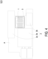
- FIG. 4 is a schematic top view illustrating an electronic device of a second embodiment of the present disclosure.
- the electronic device 101 of the present embodiment includes a first component 1, a plurality of second component 2 and a magnetic shielding element 3.
- the first component 1 for example but not limited to be an inductive component.
- the plurality of second components 2 are electronic components, and includes a first electronic component 2a, a second electronic component 2b and a third electronic component 2c.
- the first component 1, the first electronic component 2a, the second electronic component 2b and the third electronic component 2c are disposed on the same surface of the circuit board A.
- the first electronic component 2a, the second electronic component 2b and the third electronic component 2c are disposed corresponding to different sides of the first component 1.
- the magnetic shielding element 3 is a flexible sheet structure, and surrounds the periphery of the first component 1, so as to form a rectangular surrounding structure. Since the rectangular surrounding structure formed by the magnetic shielding element 3 surrounds the periphery of the first component 1, at least a part of the magnetic shielding element 3 is disposed between the first component 1 and the first electronic component 2a, at least a part of the magnetic shielding element 3 is disposed between the first component 1 and the second electronic component 2b, and at least a part of the magnetic shielding element 3 is disposed between the first component 1 and the third electronic component 2c. Due to the surrounding structure formed by the flexible magnetic shielding element 3, the magnetic interference among the first component 1 and the plurality of second components 2 are reduced.
- the first component 1 includes a first surface, a second surface, a third surface, a fourth surface, a fifth surface and a sixth surface (not shown).
- the flexible magnetic shielding element 3 surrounds the first surface, the second surface, the third surface and the fourth surface of the first component 1.
- the flexible magnetic shielding element 3 may surround the second surface, the fourth surface, the fifth surface and the sixth surface of the first component 1, or surround the first surface, the third surface, the fifth surface and the sixth surface of the first component 1, or surround the first surface, the second surface, the third surface, the fourth surface, the fifth surface and the sixth surface of the first component 1.
- the flexible magnetic shielding element 3 is formed into surrounding structures having different shapes according to practical requirements.
- the surrounding structure is for example but not limited to at least one selected from the group of circle, triangle, polygonal and irregular shape. Consequently, the advantage of high flexibility of assembling is achieved.
- FIG. 5 is a cross-sectional view illustrating an electronic device of a third embodiment of the present disclosure
- FIG. 6 is a partially enlarged view illustrating an area C of the electronic device of FIG. 5
- the electronic device 102 of the present embodiment includes a first component 1, a second component 2 and a magnetic shielding element 3.
- the first component 1 is for example but not limited to an inductive component.
- the second component 2 is a non-electronic component, for example but not limited to a casing having the function of heat dissipating.
- the circuit board A is covered by the casing (the second component 2), and an accommodation space 4 is formed between the casing and the circuit board A.
- the first component 1 is disposed on the circuit board A, and is accommodated in the accommodation space 4.
- the magnetic shielding element 3 is disposed in the accommodation space 4, and includes a magnetic shielding layer 31 and an insulation film 32.
- the insulation film 32 of the magnetic shielding element 3 is attached on a side of the magnetic shielding layer 31.
- the insulation film 32 is disposed toward the first component 1, and the magnetic shielding layer 31 is disposed toward the second component 2. Since the magnetic shielding element 3 is disposed between the first component 1 and the second component 2, the magnetic interference generated from the first component 1 is prevented from reflecting by the second component 2, and the advantage of reducing magnetic interference is achieved.
- the magnetic shielding element 3 of the present embodiment achieves the advantage of reducing magnetic interference without disposing an opening on the casing.
- the magnetic shielding layer 31 of the magnetic shielding element 3 is directly attached on a surface of the second component 2, but not limited thereto.
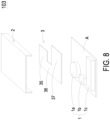
- FIG. 7 is a schematic perspective view illustrating an electronic device of a fourth embodiment of the present disclosure
- FIG. 8 is an exploded view illustrating the electronic device of FIG. 7
- the electronic device 103 of the present embodiment includes a plurality of first components 1, a second component 2 and a magnetic shielding element 3.
- the plurality of first components 1 are electronic devices, and include a first electronic component 1a, a second electronic component 1b and a third electronic component 1c.
- the second component 2 is a non-electronic component, for example but not limited to a casing having the function of heat dissipating.
- the circuit board A is covered by the casing (the second component 2), and an accommodation space 4 is formed between the casing and the circuit board A.
- the first electronic component 1 a, the second electronic component 1b and the third electronic component 1c are disposed on the same surface of the circuit board A, respectively, and accommodated in the accommodation space 4.
- the first electronic component 1a is disposed adjacent to a side of the second electronic component 1b, and the third electronic component 1c is disposed adjacent to another side of the second electronic component 1b.
- the magnetic shielding element 3 is disposed in the accommodation space 4, and is disposed between the plurality of first components 1 and the second component 2.
- the magnetic shielding element 3 includes a first portion 35, a second portion 36 and a third portion 37.
- the second portion 36 is in connection between the first portion 35 and the third portion 37.
- the magnetic shielding element 3 is attached on the second component 2, and is arranged above the first electronic component 1a, the second electronic component 1b and the third electronic component 1c.
- the first portion 35 is disposed corresponding to the position of the first electronic component 1a.
- the second portion 36 is disposed corresponding to the position of the second electronic component 1b.
- the third portion 37 is disposed corresponding to the position of the third electronic component 1c. Since the first portion 35, the second portion 36 and the third portion 37 of the magnetic shielding element 3 are disposed corresponding to the first components 1, the magnetic interference generated from the plurality of first components 1 is prevented from reflecting by the second component 2, and the advantage of reducing magnetic interference is achieved.
- the shape of the magnetic shielding element 3 can be adjusted according to the shape and position of the first component 1, which is not limited to forgoing embodiments.
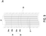
- FIG. 9 is a partially cross-sectional view illustrating a magnetic shielding element of the electronic device of a variant embodiment of the present disclosure.
- the structure of the magnetic shielding element 3a of the present embodiment is similar to the magnetic shielding element 3 of FIG. 3 , the same references represent the same components and functions, and they would not be repeatedly described hereinafter.
- the magnetic shielding element 3a of the present embodiment includes at least one protection layer 34.
- the at least one protection layer 34 for example but not limited to be two protection layers 34, and include a first protection layer 34a and a second protection layer 34b.
- the first protection layer 34a is detachably disposed on the first insulation film 32a, and is arranged at a side of the magnetic shielding layer 31.
- the second protection layer 34b is detachably disposed on the second insulation film 32b, and is arranged at another side of the magnetic shielding layer 31.
- the first protection layer 34a and the second protection layer 34b are the two outermost layers of the magnetic shielding element 3a, respectively, configured for protecting the magnetic shielding layer 31 and the insulation film 32 from being damaged or stuck during transportation.
- the first protection layer 34a and the second protection layer 34b are attached on the first insulation film 32a and the second insulation film 32b by a double-sided tape, respectively, and are removed before the assembling process of the components, but not limited thereto.
- the at least one protection layer 34 of the magnetic shielding element 3a is for example but not limited to a release film.
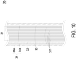
- FIG. 10 is a partially cross-sectional view illustrating a magnetic shielding element of the electronic device of another variant embodiment of the present disclosure.
- the structure of the magnetic shielding element 3b of the present embodiment is similar to the magnetic shielding element 3a of FIG. 9 , the same references represent the same components and functions, and they would not be repeatedly described hereinafter.
- the first protection layer 34a of the at least one protection layer 34 of the magnetic shielding element 3b of the present embodiment is detachably disposed on the insulation film 32, and arranged at a side of the magnetic shielding layer 31.
- the second protection layer 34b is detachably attached on another side of the magnetic shielding layer 31 opposite to the insulation film 32.
- the first protection layer 34a and the second protection layer 34b are the two outermost layers of the magnetic shielding element 3, respectively, configured for protecting the magnetic shielding layer 31 and the insulation film 32 from being damaged or stuck during transportation.
- the first protection layer 34a and the second protection layer 34b are attached on the insulation film 32 and the magnetic shielding layer 31 by a double-sided tape, respectively, and are removed before the assembling process of the components, but not limited thereto.
- the at least one protection layer 34 of the magnetic shielding element 3b is for example but not limited to a release film.
- the present disclosure provides an electronic device with low magnetic interference and a magnetic shielding element thereof.
- the magnetic shielding element By arranging the magnetic shielding element between the first component and the second component, the magnetic interference therebetween is reduced. Due to the arrangement of the insulation film of the magnetic shielding element, the insulating efficiency between the components is enhanced. Due to the arrangement of the stacked magnetic films of the magnetic shielding layer, the strength of blocking magnetic interference is increased.
- the magnetic shielding element of the present disclosure has thinner thickness and lower cost, so that the advantages of saving space and reducing cost are achieved. Since the magnetic shielding element of the present disclosure can block the magnetic interference without grounding, the advantages of easily assembling and high flexibility of use are achieved.
- the magnetic shielding element is formed as the surrounding structure, or disposed corresponding to the electronic components, the magnetic interference among the plurality of electronic components are reduced. Since the protection layers are the outermost layers of the magnetic shielding element, the advantages of protecting the magnetic shielding element from being damaged or stuck during transportation are achieved.
Landscapes
- Engineering & Computer Science (AREA)
- Power Engineering (AREA)
- Microelectronics & Electronic Packaging (AREA)
- Shielding Devices Or Components To Electric Or Magnetic Fields (AREA)
- Casings For Electric Apparatus (AREA)
Abstract
The present disclosure provides an electronic device (100, 101, 102, 103) and a magnetic shielding element (3, 3a, 3b) thereof. The electronic device (100, 101, 102, 103) includes a first component (1), a second component (2) and a magnetic shielding element (3, 3a, 3b). The first component (1) is an electronic component. The second component (2) disposed adjacent to the first component (1). At least a part of the magnetic shielding element (3, 3a, 3b) is disposed between the first component (1) and the second component (2). Consequently, the advantage of reducing the magnetic interference is achieved.
Description
- The present disclosure relates to an electronic equipment, and more particularly to an electronic device with low magnetic interference and a magnetic shielding element thereof.
- With the development and improvement of the technology, miniaturized electronic devices have become one of the current trends. The conventional electronic device, such as power adapter, usually includes a plurality of electronic components (such as transformer and inductor) and assembling components (such as casing). In order to achieve the purpose of miniaturization, the arrangement of the electronic components and the assembling components are designed to be relatively compact. However, the compacted arrangement would cause excessive magnetic interference among the plurality of electronic components. Moreover, if the electronic component is disposed closing to the assembling component, the magnetic interference from the electronic component would be reflected by the assembling component, so that the electronic component would still be affected by the magnetic interference.
- In order to overcome the above-mentioned deficiencies, some of the conventional electronic devices further include copper plates. The copper plate is perpendicularly disposed between two electronic components, and the copper plate is grounded, so as to reduce the magnetic interference between the two electronic components. However, the perpendicular copper plate has large volume, which cannot satisfy the requirement of miniaturization, and increases the difficulty of the manufacturing process of the electronic device. In addition, the cost of the copper is high, and the flexibility of use is low.
- In some conventional electronic devices, the casing (assembling component) thereof further includes an opening. The opening in disposed corresponding to the position of the electronic component. Due to the arrangement of the opening, the reflection from the casing is reduced. However, since the casing includes the opening, the heat dissipating area of the casing is reduced, and poor heat dissipation efficiency of the electronic device would be caused. Moreover, the arrangement of the opening needs extra manufacturing costs, and the manufacturing process is complicated.
- Therefore, there is a need of providing an electronic device with low magnetic interference and a magnetic shielding element thereof to obviate the drawbacks encountered from the prior arts.
- It is an objective of the present disclosure to provide an electronic device with low magnetic interference and a magnetic shielding element thereof, which achieves the advantages of reducing the magnetic interference, easily assembling, high flexibility of use, reducing cost, enhancing heat dissipating efficiency, and fulfilling the requirements of miniaturization.
- In accordance with an aspect of the present disclosure, there is provided an electronic device. The electronic device includes at least one first component, at least one second component and at least one magnetic shielding element. The at least one first component is an electronic component. The at least one second component is disposed adjacent to the at least one first component. At least a part of the at least one magnetic shielding element is disposed between the at least one first component and the at least one second component.
- In accordance with another aspect of the present disclosure, there is provided a magnetic shielding element. The magnetic shielding element is applied for an electronic device. The electronic device includes a first component and a second component. The second component is disposed adjacent to the first component. At least a part of the magnetic shielding element is disposed between the first component and the second component.
-
-
FIG. 1 is a schematic top view illustrating an electronic device of a first embodiment of the present disclosure; -
FIG. 2 is a partially enlarged view illustrating an area B of the electronic device ofFIG. 1 ; -
FIG. 3 is a partially cross-sectional view illustrating a magnetic shielding element of the electronic device ofFIG. 1 ; -
FIG. 4 is a schematic top view illustrating an electronic device of a second embodiment of the present disclosure; -
FIG. 5 is a cross-sectional view illustrating an electronic device of a third embodiment of the present disclosure; -
FIG. 6 is a partially enlarged view illustrating an area C of the electronic device ofFIG. 5 ; -
FIG. 7 is a schematic perspective view illustrating an electronic device of a fourth embodiment of the present disclosure; -
FIG. 8 is an exploded view illustrating the electronic device ofFIG. 7 ; -
FIG. 9 is a partially cross-sectional view illustrating a magnetic shielding element of the electronic device of a variant embodiment of the present disclosure; and -
FIG. 10 is a partially cross-sectional view illustrating a magnetic shielding element of the electronic device of another variant embodiment of the present disclosure. - The present disclosure will now be described more specifically with reference to the following embodiments. It is to be noted that the following descriptions of preferred embodiments of this disclosure are presented herein for purpose of illustration and description only. It is not intended to be exhaustive or to be limited to the precise form disclosed.
-
FIG. 1 is a schematic top view illustrating an electronic device of a first embodiment of the present disclosure, andFIG. 2 is a partially enlarged view illustrating an area B of the electronic device ofFIG. 1 . As shown inFIG. 1 andFIG. 2 , theelectronic device 100 of the present embodiment includes at least onefirst component 1, at least onesecond component 2 and at least onemagnetic shielding element 3. For ease of understanding, theelectronic device 100 of the present embodiment for example but not limited to include onefirst component 1, onesecond component 2 and onemagnetic shielding element 3. Thefirst component 1 is an electronic component, which for example but not limited to be an inductive component. Thesecond component 2 is an electronic component, which for example but not limited to be a transformer. Both of thefirst component 1 and thesecond component 2 are disposed on the circuit board A. Thesecond component 2 is disposed adjacent to a side of thefirst component 1. Themagnetic shielding element 3 is disposed between thefirst component 1 and thesecond component 2. Since themagnetic shielding element 3 is disposed between thefirst component 1 and thesecond component 2, the interaction caused by the magnetic interference between thefirst component 1 and thesecond component 2 is reduced. In the present embodiment, themagnetic shielding element 3 is attached on thesecond component 2, but not limited thereto. In some embodiments, themagnetic shielding element 3 is attached on thefirst component 1, or is attached on thefirst component 1 and thesecond component 2 at the same time. - In the present embodiment, the
magnetic shielding element 3 includes amagnetic shielding layer 31 and at least oneinsulation film 32. In the present embodiment, the at least oneinsulation film 32 includes afirst insulation film 32a and asecond insulation film 32b. Thefirst insulation film 32a and thesecond insulation film 32b are attached on two opposite sides of themagnetic shielding layer 31, respectively. Thefirst insulation film 32a is disposed on the side toward thefirst component 1, and thesecond insulation film 32b is disposed on the side toward thesecond component 2. Due to the arrangement of thefirst insulation film 32a and thesecond insulation film 32b of themagnetic shielding element 3, the insulating efficiency between thefirst component 1 and thesecond component 2 is enhanced. -
FIG. 3 is a partially cross-sectional view illustrating a magnetic shielding element of the electronic device ofFIG. 1 . As shown inFIG. 1 to FIG. 3 , themagnetic shielding layer 31 of themagnetic shielding element 3 of the present embodiment includes a plurality ofmagnetic films 311. The plurality ofmagnetic films 311 are stacked and adhered with each other. In the present embodiment, the number of themagnetic films 311 is five, and the fivemagnetic films 311 are stacked and adhered with each other to form themagnetic shielding layer 31, but not limited thereto, the number of themagnetic films 311 can be adjusted according to the intensity of the magnetic interference. Two adjacentmagnetic films 311 are adhered to each other by anadhesive layer 33. Theadhesive layer 33 is for example but not limited to a double-sided tape. Thefirst insulation film 32a and thesecond insulation film 32b are adhered to two opposite sides of themagnetic shielding layer 31 byadhesive layers 33, respectively. Since themagnetic shielding layer 31 includes stackedmagnetic films 311, the strength of blocking magnetic interference of themagnetic shielding element 3 is increased. By comparing to the copper plate of the prior art, themagnetic shielding element 3 of the present embodiment has thinner thickness and lower cost, so that the advantages of saving space and reducing cost are achieved. In addition, themagnetic shielding element 3 of the present embodiment blocks the magnetic interference without grounding, the advantages of easily assembling and high flexibility of use are achieved. -
FIG. 4 is a schematic top view illustrating an electronic device of a second embodiment of the present disclosure. As shown inFIG. 4 , theelectronic device 101 of the present embodiment includes afirst component 1, a plurality ofsecond component 2 and amagnetic shielding element 3. In the present embodiment, thefirst component 1 for example but not limited to be an inductive component. The plurality ofsecond components 2 are electronic components, and includes a firstelectronic component 2a, a secondelectronic component 2b and a thirdelectronic component 2c. Thefirst component 1, the firstelectronic component 2a, the secondelectronic component 2b and the thirdelectronic component 2c are disposed on the same surface of the circuit board A. The firstelectronic component 2a, the secondelectronic component 2b and the thirdelectronic component 2c are disposed corresponding to different sides of thefirst component 1. In the present embodiment, themagnetic shielding element 3 is a flexible sheet structure, and surrounds the periphery of thefirst component 1, so as to form a rectangular surrounding structure. Since the rectangular surrounding structure formed by themagnetic shielding element 3 surrounds the periphery of thefirst component 1, at least a part of themagnetic shielding element 3 is disposed between thefirst component 1 and the firstelectronic component 2a, at least a part of themagnetic shielding element 3 is disposed between thefirst component 1 and the secondelectronic component 2b, and at least a part of themagnetic shielding element 3 is disposed between thefirst component 1 and the thirdelectronic component 2c. Due to the surrounding structure formed by the flexiblemagnetic shielding element 3, the magnetic interference among thefirst component 1 and the plurality ofsecond components 2 are reduced. Thefirst component 1 includes a first surface, a second surface, a third surface, a fourth surface, a fifth surface and a sixth surface (not shown). In the present embodiment, the flexiblemagnetic shielding element 3 surrounds the first surface, the second surface, the third surface and the fourth surface of thefirst component 1. In other embodiment, the flexiblemagnetic shielding element 3 may surround the second surface, the fourth surface, the fifth surface and the sixth surface of thefirst component 1, or surround the first surface, the third surface, the fifth surface and the sixth surface of thefirst component 1, or surround the first surface, the second surface, the third surface, the fourth surface, the fifth surface and the sixth surface of thefirst component 1. - In some embodiments, the flexible
magnetic shielding element 3 is formed into surrounding structures having different shapes according to practical requirements. The surrounding structure is for example but not limited to at least one selected from the group of circle, triangle, polygonal and irregular shape. Consequently, the advantage of high flexibility of assembling is achieved. -
FIG. 5 is a cross-sectional view illustrating an electronic device of a third embodiment of the present disclosure, andFIG. 6 is a partially enlarged view illustrating an area C of the electronic device ofFIG. 5 . As shown inFIG. 5 andFIG. 6 , theelectronic device 102 of the present embodiment includes afirst component 1, asecond component 2 and amagnetic shielding element 3. In the present embodiment, thefirst component 1 is for example but not limited to an inductive component. Thesecond component 2 is a non-electronic component, for example but not limited to a casing having the function of heat dissipating. The circuit board A is covered by the casing (the second component 2), and anaccommodation space 4 is formed between the casing and the circuit board A. Thefirst component 1 is disposed on the circuit board A, and is accommodated in theaccommodation space 4. Themagnetic shielding element 3 is disposed in theaccommodation space 4, and includes amagnetic shielding layer 31 and aninsulation film 32. Theinsulation film 32 of themagnetic shielding element 3 is attached on a side of themagnetic shielding layer 31. Theinsulation film 32 is disposed toward thefirst component 1, and themagnetic shielding layer 31 is disposed toward thesecond component 2. Since themagnetic shielding element 3 is disposed between thefirst component 1 and thesecond component 2, the magnetic interference generated from thefirst component 1 is prevented from reflecting by thesecond component 2, and the advantage of reducing magnetic interference is achieved. By comparing to the prior art, themagnetic shielding element 3 of the present embodiment achieves the advantage of reducing magnetic interference without disposing an opening on the casing. Due to the casing without openings has a larger heat dissipation area, the heat dissipation efficiency is increased. In the present embodiment, themagnetic shielding layer 31 of themagnetic shielding element 3 is directly attached on a surface of thesecond component 2, but not limited thereto. -
FIG. 7 is a schematic perspective view illustrating an electronic device of a fourth embodiment of the present disclosure, andFIG. 8 is an exploded view illustrating the electronic device ofFIG. 7 . As shown inFIG. 7 andFIG. 8 , theelectronic device 103 of the present embodiment includes a plurality offirst components 1, asecond component 2 and amagnetic shielding element 3. In the present embodiment, the plurality offirst components 1 are electronic devices, and include a firstelectronic component 1a, a secondelectronic component 1b and a thirdelectronic component 1c. Thesecond component 2 is a non-electronic component, for example but not limited to a casing having the function of heat dissipating. The circuit board A is covered by the casing (the second component 2), and anaccommodation space 4 is formed between the casing and the circuit board A. The firstelectronic component 1 a, the secondelectronic component 1b and the thirdelectronic component 1c are disposed on the same surface of the circuit board A, respectively, and accommodated in theaccommodation space 4. The firstelectronic component 1a is disposed adjacent to a side of the secondelectronic component 1b, and the thirdelectronic component 1c is disposed adjacent to another side of the secondelectronic component 1b. Themagnetic shielding element 3 is disposed in theaccommodation space 4, and is disposed between the plurality offirst components 1 and thesecond component 2. Themagnetic shielding element 3 includes afirst portion 35, asecond portion 36 and athird portion 37. Thesecond portion 36 is in connection between thefirst portion 35 and thethird portion 37. Themagnetic shielding element 3 is attached on thesecond component 2, and is arranged above the firstelectronic component 1a, the secondelectronic component 1b and the thirdelectronic component 1c. Thefirst portion 35 is disposed corresponding to the position of the firstelectronic component 1a. Thesecond portion 36 is disposed corresponding to the position of the secondelectronic component 1b. Thethird portion 37 is disposed corresponding to the position of the thirdelectronic component 1c. Since thefirst portion 35, thesecond portion 36 and thethird portion 37 of themagnetic shielding element 3 are disposed corresponding to thefirst components 1, the magnetic interference generated from the plurality offirst components 1 is prevented from reflecting by thesecond component 2, and the advantage of reducing magnetic interference is achieved. In some embodiments, the shape of themagnetic shielding element 3 can be adjusted according to the shape and position of thefirst component 1, which is not limited to forgoing embodiments. -
FIG. 9 is a partially cross-sectional view illustrating a magnetic shielding element of the electronic device of a variant embodiment of the present disclosure. The structure of themagnetic shielding element 3a of the present embodiment is similar to themagnetic shielding element 3 ofFIG. 3 , the same references represent the same components and functions, and they would not be repeatedly described hereinafter. Different from themagnetic shielding element 3 ofFIG. 3 , themagnetic shielding element 3a of the present embodiment includes at least oneprotection layer 34. The at least oneprotection layer 34 for example but not limited to be twoprotection layers 34, and include afirst protection layer 34a and asecond protection layer 34b. Thefirst protection layer 34a is detachably disposed on thefirst insulation film 32a, and is arranged at a side of themagnetic shielding layer 31. Thesecond protection layer 34b is detachably disposed on thesecond insulation film 32b, and is arranged at another side of themagnetic shielding layer 31. Thefirst protection layer 34a and thesecond protection layer 34b are the two outermost layers of themagnetic shielding element 3a, respectively, configured for protecting themagnetic shielding layer 31 and theinsulation film 32 from being damaged or stuck during transportation. In the present embodiment, thefirst protection layer 34a and thesecond protection layer 34b are attached on thefirst insulation film 32a and thesecond insulation film 32b by a double-sided tape, respectively, and are removed before the assembling process of the components, but not limited thereto. In the present embodiment, the at least oneprotection layer 34 of themagnetic shielding element 3a is for example but not limited to a release film. -
FIG. 10 is a partially cross-sectional view illustrating a magnetic shielding element of the electronic device of another variant embodiment of the present disclosure. The structure of themagnetic shielding element 3b of the present embodiment is similar to themagnetic shielding element 3a ofFIG. 9 , the same references represent the same components and functions, and they would not be repeatedly described hereinafter. Different from themagnetic shielding element 3a ofFIG. 9 , thefirst protection layer 34a of the at least oneprotection layer 34 of themagnetic shielding element 3b of the present embodiment is detachably disposed on theinsulation film 32, and arranged at a side of themagnetic shielding layer 31. Thesecond protection layer 34b is detachably attached on another side of themagnetic shielding layer 31 opposite to theinsulation film 32. Thefirst protection layer 34a and thesecond protection layer 34b are the two outermost layers of themagnetic shielding element 3, respectively, configured for protecting themagnetic shielding layer 31 and theinsulation film 32 from being damaged or stuck during transportation. In the present embodiment, thefirst protection layer 34a and thesecond protection layer 34b are attached on theinsulation film 32 and themagnetic shielding layer 31 by a double-sided tape, respectively, and are removed before the assembling process of the components, but not limited thereto. In the present embodiment, the at least oneprotection layer 34 of themagnetic shielding element 3b is for example but not limited to a release film. - From the above descriptions, the present disclosure provides an electronic device with low magnetic interference and a magnetic shielding element thereof. By arranging the magnetic shielding element between the first component and the second component, the magnetic interference therebetween is reduced. Due to the arrangement of the insulation film of the magnetic shielding element, the insulating efficiency between the components is enhanced. Due to the arrangement of the stacked magnetic films of the magnetic shielding layer, the strength of blocking magnetic interference is increased. By comparing to the copper plate of the prior art, the magnetic shielding element of the present disclosure has thinner thickness and lower cost, so that the advantages of saving space and reducing cost are achieved. Since the magnetic shielding element of the present disclosure can block the magnetic interference without grounding, the advantages of easily assembling and high flexibility of use are achieved. Since the magnetic shielding element is formed as the surrounding structure, or disposed corresponding to the electronic components, the magnetic interference among the plurality of electronic components are reduced. Since the protection layers are the outermost layers of the magnetic shielding element, the advantages of protecting the magnetic shielding element from being damaged or stuck during transportation are achieved.
Claims (15)
- An electronic device (100, 101, 102, 103) characterized by comprising:at least one first component (1), wherein the at least one first component (1) is an electronic component;at least one second component (2) disposed adjacent to the at least one first component (1); andat least one magnetic shielding element (3, 3a, 3b), wherein at least a part of the at least one magnetic shielding element (3, 3a, 3b) is disposed between the at least one first component (1) and the at least one second component (2).
- The electronic device (100, 101, 102, 103) according to claim 1, wherein the at least one magnetic shielding element (3, 3a, 3b) is attached on at least one of the at least one first component (1) or the at least one second component (2), wherein the at least one magnetic shielding element (3, 3a, 3b) is a flexible sheet structure, and surrounds the periphery of the at least one first component (1) to form a surrounding structure, wherein the surrounding structure is at least one selected from the group of circle, triangle, polygonal and irregular shape.
- The electronic device (100, 101, 102, 103) according to claim 1, wherein the at least one magnetic shielding element (3, 3a, 3b) comprises a magnetic shielding layer (31) and at least one insulation film (32), wherein a surface of the at least one insulation film (32) is attached on a side of the magnetic shielding layer (31), and the at least one insulation film (32) is disposed toward the at least one first component (1).
- The electronic device (100, 101) according to claim 3, wherein the at least one second component (2) is an electronic component, wherein the at least one insulation film (32) of the at least one magnetic shielding element (3, 3a) comprises a first insulation film (32a) and a second insulation film (32b), wherein the first insulation film (32a) and the second insulation film (32b) are attached on two opposite sides of the magnetic shielding layer (31), respectively, wherein the first insulation film (32a) is disposed toward the at least one first component (1), and the second insulation film (32b) is disposed toward the at least one second component (2).
- The electronic device (102, 103) according to claim 3, wherein the at least one second component (2) is a non-electronic component, wherein the at least one insulation film (32) of the at least one magnetic shielding element (3, 3a, 3b) is attached on a side of the magnetic shielding layer (31), wherein the at least one insulation film (32) is disposed toward the at least one first component (1), and the magnetic shielding layer (31) is disposed toward the at least one second component (2), wherein the magnetic shielding layer (31) of the at least one magnetic shielding element (3, 3a, 3b) is attached on the at least one second component (2).
- The electronic device (100, 101, 102, 103) according to claim 3, wherein the magnetic shielding layer (31) of the at least one magnetic shielding element (3, 3a, 3b) comprises a plurality of magnetic films (311), wherein the plurality of magnetic films (311) are stacked and adhered with each other, wherein two adjacent magnetic films (311) are adhered to each other by a double-sided tape.
- The electronic device (100, 101, 102, 103) according to claim 3, wherein the at least one magnetic shielding element (3a, 3b) comprises at least one protection layer (34), wherein the at least one protection layer (34) is detachably disposed on a side of the magnetic shielding layer (31) or the at least one insulation film (32), and is the outermost layer of the at least one magnetic shielding element (3a, 3b).
- The electronic device (100, 101, 102, 103) according to claim 7, wherein the at least one protection layer (34) comprises a first protection layer (34a) and a second protection layer (34b), wherein the first protection layer (34a) and the second protection layer (34b) are detachable, and are two opposite outermost layers of the at least one magnetic shielding element (3a, 3b), wherein the at least one protection layer (34) of the at least one magnetic shielding element (3a, 3b) is a release film.
- A magnetic shielding element (3, 3a, 3b) for an electronic device (100, 101, 102, 103), wherein the electronic device (100, 101, 102, 103) comprises a first component (1) and a second component (2), and the second component (2) is disposed adjacent to the first component (1), characterized in that:
at least a part of the magnetic shielding element (3, 3a, 3b) is disposed between the first component (1) and the second component (2). - The magnetic shielding element (3, 3a, 3b) according to claim 9, wherein the magnetic shielding element (3, 3a, 3b) is attached on at least one of the first component (1) or the second component (2), wherein the magnetic shielding element (3, 3a, 3b) is a flexible sheet structure, and surrounds the periphery of the first component (1) to form a surrounding structure, wherein the surrounding structure is at least one selected from the group of circle, triangle, polygonal and irregular shape.
- The magnetic shielding element (3, 3a, 3b) according to claim 9, wherein the magnetic shielding element (3, 3a, 3b) comprises a magnetic shielding layer (31) and at least one insulation film (32), wherein a surface of the at least one insulation film (32) is attached on a side of the magnetic shielding layer (31), and the at least one insulation film (32) is disposed toward the first component (1).
- The magnetic shielding element (3, 3a) according to claim 11, wherein the second component (2) is an electronic component, wherein the at least one insulation film (32) comprises a first insulation film (32a) and a second insulation film (32b), wherein the first insulation film (32a) and the second insulation film (32b) are attached on two opposite sides of the magnetic shielding layer (31), respectively, wherein the first insulation film (32a) is disposed toward the first component (1), and the second insulation film (32b) is disposed toward the second component (2).
- The magnetic shielding element (3, 3a, 3b) according to claim 11, wherein the second component (2) is a non-electronic component, wherein the at least one insulation film (32) is attached on a side of the magnetic shielding layer (31), wherein the at least one insulation film (32) is disposed toward the first component (1), and the magnetic shielding layer (31) is disposed toward the second component (2), wherein the magnetic shielding layer (31) is attached on the second component (2).
- The magnetic shielding element (3, 3a, 3b) according to claim 11, wherein the magnetic shielding layer (31) comprises a plurality of magnetic films (311), wherein the plurality of magnetic films (311) are stacked and adhered with each other, wherein two adjacent magnetic films (311) are adhered to each other by a double-sided tape.
- The magnetic shielding element (3a, 3b) according to claim 11, wherein the magnetic shielding element (3a, 3b) comprises at least one protection layer (34), wherein the at least one protection layer (34) is detachably disposed on a side of the magnetic shielding layer (31) or the at least one insulation film (32), and is the outermost layer of the magnetic shielding element (3a, 3b), wherein the at least one protection layer (34) comprises a first protection layer (34a) and a second protection layer (34b), wherein the first protection layer (34a) and the second protection layer (34b) are detachable, and are two opposite outermost layers of the magnetic shielding element (3, 3a, 3b), wherein the at least one protection layer (34) of the at least one magnetic shielding element (3a, 3b) is a release film.
Applications Claiming Priority (2)
| Application Number | Priority Date | Filing Date | Title |
|---|---|---|---|
| US202363529428P | 2023-07-28 | 2023-07-28 | |
| CN202311518758.XA CN119451067A (en) | 2023-07-28 | 2023-11-15 | Electronic device and magnetic shielding member thereof |
Publications (1)
| Publication Number | Publication Date |
|---|---|
| EP4498393A1 true EP4498393A1 (en) | 2025-01-29 |
Family
ID=91828955
Family Applications (1)
| Application Number | Title | Priority Date | Filing Date |
|---|---|---|---|
| EP24186520.3A Pending EP4498393A1 (en) | 2023-07-28 | 2024-07-04 | Electronic device and magnetic shielding element thereof |
Country Status (3)
| Country | Link |
|---|---|
| US (1) | US20250037932A1 (en) |
| EP (1) | EP4498393A1 (en) |
| JP (1) | JP2025019999A (en) |
Citations (4)
| Publication number | Priority date | Publication date | Assignee | Title |
|---|---|---|---|---|
| JPH0697694A (en) * | 1992-09-16 | 1994-04-08 | Hitachi Ltd | Electromagnetic shield film and shield structure body using this film |
| WO2015158008A1 (en) * | 2014-04-18 | 2015-10-22 | 华为终端有限公司 | Shielding film, shielding circuit board and terminal device |
| EP3182815A1 (en) * | 2015-12-15 | 2017-06-21 | Samsung Electronics Co., Ltd | Electronic device including shield structure |
| US20180240582A1 (en) * | 2017-02-21 | 2018-08-23 | Samsung Electro-Mechanics Co., Ltd. | Magnetic sheet and electronic device |
Family Cites Families (4)
| Publication number | Priority date | Publication date | Assignee | Title |
|---|---|---|---|---|
| JPH08279690A (en) * | 1995-04-07 | 1996-10-22 | Daido Steel Co Ltd | Adhesive sheet for low frequency / low magnetic field shield and low frequency / low magnetic field shield container using the same |
| JP3900559B2 (en) * | 1996-09-19 | 2007-04-04 | 大同特殊鋼株式会社 | Magnetic shielding sheet, manufacturing method thereof, and cable using the same |
| JP2011120432A (en) * | 2009-12-07 | 2011-06-16 | Sanyo Electric Co Ltd | Power transportation system, power receiver, and method of manufacturing the power receiver |
| JP6025015B2 (en) * | 2012-02-27 | 2016-11-16 | 日立金属株式会社 | Magnetic sheet, transmission coil component and non-contact charging device |
-
2024
- 2024-02-16 US US18/443,611 patent/US20250037932A1/en active Pending
- 2024-06-11 JP JP2024094615A patent/JP2025019999A/en active Pending
- 2024-07-04 EP EP24186520.3A patent/EP4498393A1/en active Pending
Patent Citations (4)
| Publication number | Priority date | Publication date | Assignee | Title |
|---|---|---|---|---|
| JPH0697694A (en) * | 1992-09-16 | 1994-04-08 | Hitachi Ltd | Electromagnetic shield film and shield structure body using this film |
| WO2015158008A1 (en) * | 2014-04-18 | 2015-10-22 | 华为终端有限公司 | Shielding film, shielding circuit board and terminal device |
| EP3182815A1 (en) * | 2015-12-15 | 2017-06-21 | Samsung Electronics Co., Ltd | Electronic device including shield structure |
| US20180240582A1 (en) * | 2017-02-21 | 2018-08-23 | Samsung Electro-Mechanics Co., Ltd. | Magnetic sheet and electronic device |
Also Published As
| Publication number | Publication date |
|---|---|
| US20250037932A1 (en) | 2025-01-30 |
| JP2025019999A (en) | 2025-02-07 |
Similar Documents
| Publication | Publication Date | Title |
|---|---|---|
| JP4802615B2 (en) | LC composite parts | |
| US7924568B2 (en) | Heat sink device with a shielding member | |
| US6732428B1 (en) | Method for increasing electronic component density on an electronic circuit board | |
| TW200906274A (en) | Chassis base assembly and display device including the same | |
| US20080284551A1 (en) | Transformers and winding units thereof | |
| US20040183959A1 (en) | Liquid crystal display device having flexible substrates | |
| US7135644B1 (en) | Permeable conductive shield having a laminated structure | |
| US6348653B1 (en) | Apparatus for shielding a plasma display panel | |
| US7433178B2 (en) | Plasma display apparatus | |
| CN111343844B (en) | Housing for accommodating electronic devices and electronic systems having the housing | |
| US9906157B2 (en) | Package assembly | |
| JP5144210B2 (en) | Semiconductor device | |
| US7061361B2 (en) | Circuit board assembly and flat coil | |
| KR100708643B1 (en) | Plasma display | |
| US11032904B2 (en) | Interposer substrate and circuit module | |
| US20250037932A1 (en) | Electronic device and magnetic shielding element thereof | |
| JP7840395B2 (en) | Integrated resonant capability of printed circuit boards for planar transformers | |
| US5708568A (en) | Electronic module with low impedance ground connection using flexible circuits | |
| CN110290632A (en) | A kind of electronic device of electrostatic discharge protective | |
| TW201014475A (en) | Printed circuit board and electronic device | |
| TWI869050B (en) | Electronic device and magnetic shielding element thereof | |
| KR100615174B1 (en) | Plasma display | |
| JP3678113B2 (en) | Printed circuit manufacturing method and portable communication device | |
| JP2000196250A (en) | Electronic circuit board protection device | |
| CN222869281U (en) | Circuit board assembly and electronic equipment |
Legal Events
| Date | Code | Title | Description |
|---|---|---|---|
| PUAI | Public reference made under article 153(3) epc to a published international application that has entered the european phase |
Free format text: ORIGINAL CODE: 0009012 |
|
| STAA | Information on the status of an ep patent application or granted ep patent |
Free format text: STATUS: THE APPLICATION HAS BEEN PUBLISHED |
|
| AK | Designated contracting states |
Kind code of ref document: A1 Designated state(s): AL AT BE BG CH CY CZ DE DK EE ES FI FR GB GR HR HU IE IS IT LI LT LU LV MC ME MK MT NL NO PL PT RO RS SE SI SK SM TR |
|
| STAA | Information on the status of an ep patent application or granted ep patent |
Free format text: STATUS: REQUEST FOR EXAMINATION WAS MADE |
|
| 17P | Request for examination filed |
Effective date: 20250221 |