EP4485800A2 - Zufallszahlengenerator - Google Patents
Zufallszahlengenerator Download PDFInfo
- Publication number
- EP4485800A2 EP4485800A2 EP24208861.5A EP24208861A EP4485800A2 EP 4485800 A2 EP4485800 A2 EP 4485800A2 EP 24208861 A EP24208861 A EP 24208861A EP 4485800 A2 EP4485800 A2 EP 4485800A2
- Authority
- EP
- European Patent Office
- Prior art keywords
- input
- flip
- output
- circuit
- inputs
- Prior art date
- Legal status (The legal status is an assumption and is not a legal conclusion. Google has not performed a legal analysis and makes no representation as to the accuracy of the status listed.)
- Granted
Links
Images

Classifications
-
- G—PHYSICS
- G06—COMPUTING OR CALCULATING; COUNTING
- G06F—ELECTRIC DIGITAL DATA PROCESSING
- G06F7/00—Methods or arrangements for processing data by operating upon the order or content of the data handled
- G06F7/58—Random or pseudo-random number generators
-
- H—ELECTRICITY
- H03—ELECTRONIC CIRCUITRY
- H03K—PULSE TECHNIQUE
- H03K3/00—Circuits for generating electric pulses; Monostable, bistable or multistable circuits
- H03K3/84—Generating pulses having a predetermined statistical distribution of a parameter, e.g. random pulse generators
Definitions
- the invention concerns a random number generator intended especially for generating truly random numbers and series.
- a ring oscillator comprise a delay line closed in a loop, where an input and an output are connected with each other and connected to an output of the ring oscillator.
- the delay line comprise delays connected in series and connected between the input and the output of the delay line.
- a random number generator comprising two ring oscillators a phase detector. Outputs of two ring oscillators are connected to inputs of the phase detector, whereas an output of the phase detector is connected to an output of the random number generator through a von Neumann corrector.
- a ring oscillator comprise a delay line closed in a loop, where an input and an output are connected with each other and connected to an output of the ring oscillator.
- the delay line comprise delays connected in series and connected between the input and the output of the delay line.
- the aim of the invention is to provide nondeterministic phases of signals at the inputs of phase detectors as well as nondeterministic initialization of multiple metastability processes.
- Random number generator comprising a first bistable, having an output connected to a first output of the random number generator and comprising two ring oscillators, having outputs connected to inputs of the bistable, whereas the ring oscillators comprise delay lines closed in a loops, and the delay lines comprise delays connected in series between inputs and outputs of the delay lines, according to the invention comprises at least one additional bistable, having output connected to an additional output of the random number generator, whereas the additional bistable has a first input connected to the delay line of one of the ring oscillators and a second input connected to the delay line of another of the ring oscillators.
- the effect of such a construction allows to obtain at least one additional, substantially independent random process on the additional output of the random number generator.
- Random number generator advantageously comprises at least one more ring oscillator.
- the effect is that the bistables connected to different ring oscillators are stimulated with less correlated signals than the bistables connected to the same ring oscillators.
- Random number generator advantageously comprises at least two bistables connected to the delay lines so, that the inputs of the bistables are separated in the delay lines with at least one delay. Such a solution assures that the delays are driven by bistables in the minimal manner.
- Random number generator advantageously comprises at least two bistables, having at least one of the inputs connected to different delay lines of different ring oscillators. Such a solution assures that the bistables are stimulated with different pair of ring oscillators, and thus with different processes resulting in phase shifts.
- At least one of the additional bistables is connected with the first input to a series of delays of a delay line of one of the ring oscillators after a delay having the first number in this series counting from the beginning of the delay line.
- the second input is connected to a series of delays of a delay line of another ring oscillator after a delay having the second number in this series counting from the beginning of the delay line.
- the first number is different from the second number.
- At least two bistables advantageously are connected with at least one input each in the same place of at least one delay line. Having different bistables connected in the same places causes that the bistables are triggered with exactly the same signal.
- At least one of the bistables advantageously is a phase detector.
- Phase detector provides a precise detection of the edge priority of input waveforms, which is used for phase correction.
- At least one phase detector advantageously consists of a flip-flop with two inputs being the inputs of the phase detector and an output being the output of the phase detector.
- At least one phase detector comprises two flip-flops each having two inputs and two outputs, wherein the inputs of the flip-flops are connected to inputs of the phase detector, and outputs of the flip-flops are connected to outputs of the phase detector. Further the first input of the phase detector is connected to both the first input of the first flip-flop and the second input of the second flip-flop. Further the second input of the phase detector is connected to both the second input of the first flip-flop and the first input of the second flip-flop. Further the output of the phase detector is connected to chosen outputs of the flip-flops through a logic circuit.
- At least one of the bistables advantageously is a metastability circuit.
- a metastability circuit provides a random response of the circuit in the case of proximity of the edges of the input waveforms. More specifically, for phase shifts that do not fit in the metastability window, the metastability circuit provides a phase detection and is used to correct the phase of the ring oscillators connected to its inputs. However, for phase shifts located in the metastability window, the metastability circuit provides a random value on its output and consequently induces a random phase change, which differs the this circuit from the phase detector.
- At least one metastability circuit advantageously consists of a flip-flop with two inputs being the inputs of the metastability circuit and an output being the output of the metastability circuit.
- At least one metastability circuit comprises a metastable circuit with an oscillatory response with two inputs being the inputs of the metastability circuit and an output being the output of the metastability circuit.
- the output of the metastable circuit with an oscillatory response advantageously is connected to the output of the metastability circuit through an adder and advantageously the metastability circuit comprises counter, having outputs connected to consecutive inputs of the adder, and having an input connected to the output of the metastable circuit with an oscillatory response.
- At least one metastability circuit comprises a metastable generator of time intervals, having inputs connected to the inputs of the metastability circuit and outputs connected to inputs of an arbiter circuit, having outputs connected to the outputs of the metastability circuit through a logic circuit.
- the metastable generator of time intervals comprises two flip-flops having two inputs and single outputs, wherein the inputs of the flip-flops of the metastable generator of time intervals are connected to the inputs of the metastability circuit and wherein, the first input of the metastability circuit is connected to both the first input of the first flip-flop and the first input of the second flip-flop, the second input of the metastability circuit is connected to both the second input of the first flip-flop and the second input of the second flip-flop.
- the arbiter circuit comprises two flip-flops having two inputs and two outputs each, wherein the outputs of the flip-flops of the metastable generator of time intervals are connected to the inputs of the flip-flops of the arbiter circuit and wherein, the output of the first flip-flop of the metastable generator of time intervals is connected to both the first input of the first flip-flop of the arbiter circuit and the second input of the second flip-flop of the arbiter circuit, the output of the second flip-flop of the metastable generator of time intervals is connected to both the second input of the first flip-flop of the arbiter circuit and the first input of the second flip-flop of the arbiter circuit.
- the logic circuit consists of a conjunction gate, through which selected outputs of the flip-flops of the arbiter circuit are connected to the outputs of the metastability circuit.
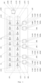
- Fig.1 presents a block diagram of random number generator with two ring oscillators
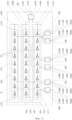
- fig.2 presents a block diagram of random number generator with three ring oscillators
- fig.4 presents a block diagram of phase detector comprising two flip-flops
- fig.5 presents a block diagram of metastability circuit that consists of flip-flop
- fig.6 presents a block diagram of metastability circuit comprising metastable circuit with an oscillatory response
- fig.7 presents a block diagram of metastability circuit comprising metastable circuit with an oscillatory response and adder
- fig.8 presents a block diagram of metastability circuit comprising metastable circuit with an oscillatory response, adder and counter
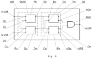
- fig.9 presents a block diagram of metastability circuit comprising metastable generator of time intervals and arbiter circuit.
- Random number generator presented in fig.1 comprises two ring oscillators GP1 and GP2 and seven bistables UB1, UB2, UB3, UB4, UB5, UB6 and UB7.
- the ring oscillators GP1 and GP2 comprise delay lines L01 and LO2 closed in loops so, that an output o-LO1 and o-LO2 of a delay line L01 and LO2 is connected to an input i-LO1 and i-L02 of this delay line and also the outputs of the delay lines L01 and LO2 are connected to outputs of the ring oscillators GP1 and GP2.
- the delay lines L01 and LO2 comprise delays EO connected in series between the inputs i-LO1 and i-L02 and the outputs o-LO1 and o-LO2 of these delay lines.
- Outputs o-UB1, o-UB2, o-UB3, o-UB4, o-UB5, o-UB6 and o-UB7 of the bistables UB1, UB2, UB3, UB4, UB5, UB6 and UB7 are connected to outputs o1-GL, o2-GL, o3-GL, o4-GL, o5-GL, o6-GL and o7-GL of the random number generator GL.
- First input i1-UB1 of the first bistable UB1 is connected to the delay line L01 of the first ring oscillator GP1 to an output of the last delay EO counting from the beginning of this delay line.
- Second input 12-UB1 of the first bistable UB1 is connected to the delay line LO2 of the second ring oscillator GP2 to an output of the last delay EO counting from the beginning of this delay line.
- First input 11-UB2 of the second bistable UB2 is connected to the delay line L01 of the first ring oscillator GP1 to an output of the first delay EO counting from the beginning of this delay line.
- Second input i2-UB2 of the second bistable UB2 is connected to the delay line LO2 of the second ring oscillator GP2 to an output of the first delay EO counting from the beginning of this delay line.
- First input 11-UB3 of the third bistable UB3 is connected to the delay line L01 of the first ring oscillator GP1 to an output of the second delay EO counting from the beginning of this delay line.
- Second input i2-UB3 of the third bistable UB3 is connected to the delay line LO2 of the second ring oscillator GP2 to an output of the second delay EO counting from the beginning of this delay line.
- First input 11-UB4 of the fourth bistable UB4 is connected to the delay line L01 of the first ring oscillator GP1 to an output of the fourth delay EO counting from the beginning of this delay line.
- Second input i2-UB4 of the fourth bistable UB4 is connected to the delay line LO2 of the second ring oscillator GP2 to an output of the fifth delay EO counting from the beginning of this delay line.
- First input 11-UB5 of the fifth bistable UB5 is connected to the delay line L01 of the first ring oscillator GP1 to an output of the fifth delay EO counting from the beginning of this delay line.
- Second input i2-UB5 of the fifth bistable UB5 is connected to the delay line LO2 of the second ring oscillator GP2 to an output of the seventh delay EO counting from the beginning of this delay line.
- First input 11-UB6 of the sixth bistable UB6 is connected to the delay line L01 of the first ring oscillator GP1 to an output of the eighth delay EO counting from the beginning of this delay line.
- Second input i2-UB6 of the sixth bistable UB6 is connected to the delay line LO2 of the second ring oscillator GP2 to an output of the eighth delay EO counting from the beginning of this delay line.
- First input 11-UB7 of the seventh bistable UB7 is connected to the delay line L01 of the first ring oscillator GP1 to an output of the eighth delay EO counting from the beginning of this delay line.
- Second input i2-UB7 of the seventh bistable UB7 is connected to the delay line LO2 of the second ring oscillator GP2 to an output of the eighth delay EO counting from the beginning of this delay line.
- the first three of the bistables UB1, UB2 and UB3 are connected to delay lines in the way that assures the delays EO are driven by bistables in the minimal manner and at the same time the bistables are stimulated by similar signals - that is, similar phase shifts of the signals of the ring oscillators GP1 and GP2.
- the third, the fourth and the fifth of the bistables UB3, UB4 and UB5 are also connected to delay lines in the way that assures the delays EO are driven by bistables in the minimal manner, however each of these bistables is stimulated by completely different phase shift of signals of the ring oscillators GP1 and GP2.
- the sixth bistable UM6 is stimulated by the same signals as the seventh bistable UM7.
- bistables UM6 and UM7 provide similar conditions for their stimulation, whereas their different structure - in particular symmetrical with respect to one another, but with asymmetrical operating characteristics - ensures the stimulation of these circuits at different phase shifts.
- the number of delays and the delay caused by each delay EO determine the basic operating frequencies of the ring oscillators GP1 and GP2.
- the basic frequency has a random component, resulting from physical phenomena - typical for electronic circuits (noise, thermal phenomena, jitter, etc.) - and because of that the signal phase also manifests random changes.
- the positive or negative phase offset of the input signals of a bistable being a phase detector provides random values at the output of the phase detector.
- the proximity of the oscillators' phases means time closeness of the edges of generated signals, which are used to stimulate bistables being metastability circuits, which produce random phenomena.
- the exceptions are the bistables connected to the delay lines with particular shifts, because the goal is to achieve a different phase stimulation - shifted by one or multiple propagation times of a delay EO.
- Random number generator presented in fig.2 comprises three ring oscillators GP1, GP2 and GP3 and seven bistables UB1, UB2, UB3, UB4, UB5, UB6 and UB7.
- the ring oscillators GP1, GP2 and GP3 comprise delay lines LO1, LO2 and LO3 closed in loops so, that an output o-LO1, o-LO2 and o-LO3 of a delay line LO1, LO2 and LO3 is connected to an input i-LO1, i-L02 and i-L03 of this delay line and also the outputs of the delay lines o-LO1, o-LO2 and o-LO3 are connected to outputs of the ring oscillators o-GP1, o-GP2 and o-GP3.
- the delay lines LO1, LO2 and LO3 comprise delays EO connected in series between the inputs i-LO1, i-L02 and i-L03 and the outputs o-LO1, o-LO2 and o-LO3 of these delay lines.
- Outputs o-UB1, o-UB2, o-UB3, o-UB4, o-UB5, o-UB6 and o-UB7 of the bistables UB1, UB2, UB3, UB4, UB5, UB6 and UB7 are connected to outputs o1-GL, o2-GL, o3-GL, o4-GL, o5-GL, o6-GL and o7-GL of the random number generator GL.
- First input i1-UB1 of the first bistable UB1 is connected to the delay line L01 of the first ring oscillator GP1 to an output of the last delay EO counting from the beginning of this delay line.
- Second input 12-UB1 of the first bistable UB1 is connected to the delay line LO2 of the second ring oscillator GP2 to an output of the last delay EO counting from the beginning of this delay line.
- First input 11-UB2 of the second bistable UB2 is connected to the delay line L01 of the first ring oscillator GP1 to an output of the first delay EO counting from the beginning of this delay line.
- Second input i2-UB2 of the second bistable UB2 is connected to the delay line LO3 of the third ring oscillator GP3 to an output of the first delay EO counting from the beginning of this delay line.
- First input 11-UB3 of the third bistable UB3 is connected to the delay line LO2 of the second ring oscillator GP2 to an output of the second delay EO counting from the beginning of this delay line.
- Second input i2-UB3 of the third bistable UB3 is connected to the delay line LO3 of the third ring oscillator GP3 to an output of the second delay EO counting from the beginning of this delay line.
- First input 11-UB4 of the fourth bistable UB4 is connected to the delay line L01 of the first ring oscillator GP1 to an output of the fourth delay EO counting from the beginning of this delay line.
- Second input i2-UB4 of the fourth bistable UB4 is connected to the delay line LO2 of the second ring oscillator GP2 to an output of the fifth delay EO counting from the beginning of this delay line.
- First input 11-UB5 of the fifth bistable UB5 is connected to the delay line L01 of the first ring oscillator GP1 to an output of the fifth delay EO counting from the beginning of this delay line.
- Second input i2-UB5 of the fifth bistable UB5 is connected to the delay line LO2 of the second ring oscillator GP2 to an output of the seventh delay EO counting from the beginning of this delay line.
- First input 11-UB6 of the sixth bistable UB6 is connected to the delay line L01 of the first ring oscillator GP1 to an output of the eighth delay EO counting from the beginning of this delay line.
- Second input i2-UB6 of the sixth bistable UB6 is connected to the delay line LO3 of the third ring oscillator GP3 to an output of the eighth delay EO counting from the beginning of this delay line.
- First input 11-UB7 of the seventh bistable UB7 is connected to the delay line L01 of the first ring oscillator GP1 to an output of the eighth delay EO counting from the beginning of this delay line.
- Second input i2-UB7 of the seventh bistable UB7 is connected to the delay line LO3 of the third ring oscillator GP3 to an output of the eighth delay EO counting from the beginning of this delay line.
- the first three of the bistables UB1, UB2 and UB3 are connected to delay lines in the way that assures the delays EO are driven by bistables in the minimal manner and at the same time the bistables are stimulated by similar signals - that is, similar phase shifts of the signals of the ring oscillators GP1 and GP2, GP1 and GP3, GP2 and GP3.
- the stimulations of bistables connected to different ring oscillators are uncorrelated or slightly correlated, which improves the randomness of numbers on the outputs of these circuits.
- the first, the fourth and the fifth of the bistables UB1, UB4 and UB5 are also connected to delay lines in the way that assures the delays EO are driven by bistables in the minimal manner, however each of these bistables is stimulated by completely different phase shift of signals of the ring oscillators GP1 and GP2.
- the sixth bistable UM6 is stimulated by the same signals as the seventh bistable UM7.
- the identical structure of these two bistables UM6 and UM7 provides similar conditions for their stimulation, whereas their different structure - in particular symmetrical with respect to one another, but with asymmetrical operating characteristics - ensures the stimulation of these circuits at different phase shifts.
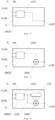
- Phase detector presented in fig.3 consists of a flip-flop P having two inputs D and C being the inputs i1-DF and i2-DF of the phase detector DF, and an output Q being the output of the phase detector o-DF.
- the logic '1' or logic '0' will appear on the output Q.
- the type of the flip-flop - e.g., D flip-flop, RS flip-flop, JK flip-flop etc. - is of secondary importance, as long as the flip-flop detects which of the input signals slopes came first.
- Phase detector presented in fig.4 comprises a logic circuit AND having two inputs and one output as well as two flip-flops P1 and P2, having two inputs D1, C1 and D2, C2 each as well as two outputs Q1, nQ1 and Q2, nQ2 each.
- the inputs of the flip-flops are connected to inputs of the phase detector DF, whereas the outputs of the flip-flops are connected to outputs of the phase detector through the logic circuit AND.
- the first input of the phase detector i1-DF is connected to both the first input of the first flip-flop D1 and the second input of the second flip-flop C2.
- the second input of the phase detector i2-DF is connected to both the second input of the first flip-flop C1 and the first input of the second flip-flop D2.
- the inputs of the logic circuit AND are connected to the second output of the first flip-flop nQ1 and the first output of the second flip-flop Q2.
- the output of the logic circuit AND is connected to the output of the phase detector o-DF.
- the phase detector composed of two flip-flops provides symmetrical detection of negative and positive phase shifts.
- Metastability circuit presented in fig.5 consists of a flip-flop Pa having two inputs Da and Ca being the inputs il-UM and 12-UM of the metastability circuit UM, and an output Qa being the output of the metastability circuit o-UM.
- the flip-flop Pa is characterized by the fact that the proximity of the edges of signals on the inputs of the flip-flop Da and Ca causes a metastable range of operation resulting in a random logic state on the output Qa.
- the type of the flip-flop - e.g., D flip-flop, RS flip-flop, JK flip-flop etc. - is of secondary importance, as long as the flip-flop provides a random response at the output in case of appropriate proximity of the edges of the input signals.
- Metastability circuit presented in fig.6 comprise a metastable circuit with an oscillatory response UMOO having two inputs R and S being the inputs il-UM and 12-UM of the metastability circuit UM, and an output wOO being the output of the metastability circuit o-UM.
- the flip-flop UMOO is characterized by the fact that the proximity of the edges of signals on the inputs of the flip-flop R and S causes a metastable range of operation resulting in oscillatory response of the flip-flop with a variable number of oscillations as well as in a random response at the output wOO.
- Metastability circuit presented in fig.7 has the same construction as the one presented in fig.6 , wherein the output wOO of the metastable circuit with an oscillatory response UMOO is connected to the output of the metastability circuit o-UM through an adder SUM.
- the adder SUM is used for adding up a variable number of oscillations at the output wOO.
- Metastability circuit presented in fig.8 has the same construction as the one presented in fig.7 , wherein it additionally comprises a counter LCZ, having outputs connected to consecutive inputs of the adder SUM and having an input i-LCZ connected to the output of the metastable circuit with an oscillatory response wOO.
- the counter LCZ is used for counting a variable number of oscillations at the output wOO, which then adds the adder SUM. Moreover, the logical state at the output wOO is also taken into account in this circuit.
- Metastability circuit presented in fig.9 comprises a metastable generator of time intervals GMIC, an arbiter circuit ARB and a logic circuit AND.
- the metastable generator of time intervals GMIC comprises two flip-flops Pb and Pc, having two inputs Db and Cb as well as Dc and Cc each, and having single outputs Qb and Qc each.
- the arbiter circuit ARB comprises two flip-flops Pd and Pe, having two inputs Dd and Cd as well as De and Ce each, and having two outputs Qd and nQd as well as Qe and nQe each.
- the logic circuit AND has two inputs and one output.
- the inputs of the flip-flops of the metastable generator of time intervals GMIC are connected to the inputs of the metastability circuit UM so, that the first input of the metastability circuit il-UM is connected to both the first input of the first flip-flop Db and the first input of the second flip-flop Dc, whereas the second input of the metastability circuit 12-UM is connected to both the second input of the first flip-flop Cb and the second input of the second flip-flop Cc.
- the outputs of the flip-flops Qb and Qc are connected to the inputs of the flip-flops of the arbiter circuit ARB so, that the output of the first flip-flop Qb is connected to both the first input of the first flip-flop of the arbiter circuit Dd and the second input of the second flip-flop of the arbiter circuit Ce, whereas the output of the second flip-flop Qc is connected to both the second input of the first flip-flop of the arbiter circuit Cd and the first input of the second flip-flop of the arbiter circuit De.
- the output of the metastability circuit o-UM is connected to the outputs of the flip-flops of the arbiter circuit nQd and Qe through the logic circuit AND.
- the inputs of the logic circuit AND are connected to the second output of the first flip-flop of the arbiter circuit nQd and the first output of the second flip-flop of the arbiter circuit Qe.
- the output of the logic circuit AND is connected to the output of the metastability circuit o-UM.
- the flip-flops Pb and Pc of the metastable generator of time intervals GMIC digital signals with relatively close proximity of the edges of the signals at the inputs of the flip-flops, causes metastable states in them, which result in logical values at the outputs Qb and Qc in various moments. Both the logical values and the time intervals are sources of randomness with specific properties of these randomities.
- the arbiter circuit compares the response times of the flip-flops Pb and Pc, and the result of this comparison - which is a random value - is interpreted by the logic circuit AND as logical zero or logical one.
- the invention can be applied and used in generating truly random numbers and series.
Landscapes
- Engineering & Computer Science (AREA)
- Theoretical Computer Science (AREA)
- General Physics & Mathematics (AREA)
- Physics & Mathematics (AREA)
- Mathematical Analysis (AREA)
- Pure & Applied Mathematics (AREA)
- Mathematical Optimization (AREA)
- General Engineering & Computer Science (AREA)
- Computational Mathematics (AREA)
- Manipulation Of Pulses (AREA)
- Control Of Eletrric Generators (AREA)
- Stabilization Of Oscillater, Synchronisation, Frequency Synthesizers (AREA)
- Bus Control (AREA)
- Pulse Circuits (AREA)
Applications Claiming Priority (4)
| Application Number | Priority Date | Filing Date | Title |
|---|---|---|---|
| PL425586A PL235106B1 (pl) | 2018-05-17 | 2018-05-17 | Generator losowy |
| PL425585A PL235105B1 (pl) | 2018-05-17 | 2018-05-17 | Generator losowy |
| EP18918533.3A EP3794728B1 (de) | 2018-05-17 | 2018-08-07 | Zufallszahlengenerator |
| PCT/IB2018/055940 WO2019220193A1 (en) | 2018-05-17 | 2018-08-07 | Random number generator |
Related Parent Applications (2)
| Application Number | Title | Priority Date | Filing Date |
|---|---|---|---|
| EP18918533.3A Division EP3794728B1 (de) | 2018-05-17 | 2018-08-07 | Zufallszahlengenerator |
| EP18918533.3A Division-Into EP3794728B1 (de) | 2018-05-17 | 2018-08-07 | Zufallszahlengenerator |
Publications (4)
| Publication Number | Publication Date |
|---|---|
| EP4485800A2 true EP4485800A2 (de) | 2025-01-01 |
| EP4485800A3 EP4485800A3 (de) | 2025-04-09 |
| EP4485800C0 EP4485800C0 (de) | 2025-09-10 |
| EP4485800B1 EP4485800B1 (de) | 2025-09-10 |
Family
ID=68540694
Family Applications (2)
| Application Number | Title | Priority Date | Filing Date |
|---|---|---|---|
| EP18918533.3A Active EP3794728B1 (de) | 2018-05-17 | 2018-08-07 | Zufallszahlengenerator |
| EP24208861.5A Active EP4485800B1 (de) | 2018-05-17 | 2018-08-07 | Zufallszahlengenerator |
Family Applications Before (1)
| Application Number | Title | Priority Date | Filing Date |
|---|---|---|---|
| EP18918533.3A Active EP3794728B1 (de) | 2018-05-17 | 2018-08-07 | Zufallszahlengenerator |
Country Status (3)
| Country | Link |
|---|---|
| EP (2) | EP3794728B1 (de) |
| PL (7) | PL4485800T3 (de) |
| WO (1) | WO2019220193A1 (de) |
Citations (1)
| Publication number | Priority date | Publication date | Assignee | Title |
|---|---|---|---|---|
| US20110169580A1 (en) | 2010-01-08 | 2011-07-14 | James Dodrill | Inverting gate with maximized thermal noise in random number genertion |
Family Cites Families (6)
| Publication number | Priority date | Publication date | Assignee | Title |
|---|---|---|---|---|
| US5153532A (en) * | 1989-05-24 | 1992-10-06 | Honeywell Inc. | Noise generator using combined outputs of two pseudo-random sequence generators |
| US6522210B1 (en) * | 2000-02-16 | 2003-02-18 | Honeywell International Inc. | Random pulse generator |
| US8583712B2 (en) * | 2007-09-18 | 2013-11-12 | Seagate Technology Llc | Multi-bit sampling of oscillator jitter for random number generation |
| KR101987141B1 (ko) * | 2013-03-04 | 2019-10-01 | 삼성전자주식회사 | 난수 발생기 |
| US9335972B2 (en) * | 2013-11-29 | 2016-05-10 | The Regents Of The University Of Michigan | True random number generator |
| WO2017146650A1 (en) * | 2016-02-24 | 2017-08-31 | Agency For Science, Technology And Research | True random number generator and system comprising the same |
-
2018
- 2018-08-07 PL PL24208861.5T patent/PL4485800T3/pl unknown
- 2018-08-07 EP EP18918533.3A patent/EP3794728B1/de active Active
- 2018-08-07 PL PL428401A patent/PL241526B1/pl unknown
- 2018-08-07 EP EP24208861.5A patent/EP4485800B1/de active Active
- 2018-08-07 WO PCT/IB2018/055940 patent/WO2019220193A1/en not_active Ceased
-
2024
- 2024-12-27 PL PL450736A patent/PL450736A3/pl unknown
- 2024-12-27 PL PL450737A patent/PL450737A3/pl unknown
- 2024-12-27 PL PL450734A patent/PL450734A3/pl unknown
- 2024-12-27 PL PL450738A patent/PL450738A3/pl unknown
- 2024-12-27 PL PL450735A patent/PL450735A3/pl unknown
Patent Citations (1)
| Publication number | Priority date | Publication date | Assignee | Title |
|---|---|---|---|---|
| US20110169580A1 (en) | 2010-01-08 | 2011-07-14 | James Dodrill | Inverting gate with maximized thermal noise in random number genertion |
Non-Patent Citations (1)
| Title |
|---|
| PIOTR Z. WIECZOREK: "Secure TRNG with Random Phase Stimulation", IEEE-SPIE JOINT SYMPOSIUM ON PHOTONICS, WEB ENGINEERING, ELECTRONICS FOR ASTRONOMY AND HIGH ENERGY PHYSICS EXPERIMENTS, vol. 10445, 2017, XP060091482, ISBN: 9781510613546, DOI: 10.1117/12.2280979 |
Also Published As
| Publication number | Publication date |
|---|---|
| PL450736A3 (pl) | 2026-04-13 |
| PL450738A3 (pl) | 2026-01-19 |
| PL241526B1 (pl) | 2022-10-17 |
| PL450737A3 (pl) | 2026-03-02 |
| PL428401A1 (pl) | 2020-07-27 |
| EP4485800A3 (de) | 2025-04-09 |
| PL4485800T3 (pl) | 2025-10-27 |
| EP4485800C0 (de) | 2025-09-10 |
| EP3794728B1 (de) | 2026-07-01 |
| WO2019220193A1 (en) | 2019-11-21 |
| EP4485800B1 (de) | 2025-09-10 |
| PL450734A3 (pl) | 2026-05-25 |
| EP3794728A4 (de) | 2022-03-16 |
| EP3794728A1 (de) | 2021-03-24 |
| PL450735A3 (pl) | 2026-01-19 |
Similar Documents
| Publication | Publication Date | Title |
|---|---|---|
| US6906562B1 (en) | Counter-based clock multiplier circuits and methods | |
| US8531322B2 (en) | Time-to-digital converter | |
| WO2010036449A2 (en) | Method and apparatus for counter-based clock signal adaptation | |
| US6906571B1 (en) | Counter-based phased clock generator circuits and methods | |
| JP2001117666A (ja) | 非整数周波数分割装置 | |
| US7236557B1 (en) | Counter-based clock multiplier circuits and methods | |
| JP2004519958A (ja) | 分数分周器付きボーレート発生器 | |
| KR100630342B1 (ko) | 락 검출기능을 구비한 위상동기루프 회로 및 위상동기루프회로의 락 검출방법 | |
| US5045715A (en) | Circuit for generating stretched clock phases on a cycle by cycle basis | |
| US11366640B2 (en) | Random number generator with a bistable and ring oscillators | |
| JP4371598B2 (ja) | 逓倍クロック発生回路 | |
| EP3794728A1 (de) | Zufallszahlengenerator | |
| PL236965B1 (pl) | Generator losowy | |
| US7358782B2 (en) | Frequency divider and associated methods | |
| PL237196B1 (pl) | Generator losowy | |
| JP2015015540A (ja) | Emi対策回路 | |
| TWI804192B (zh) | 數位鎖相環電路 | |
| EP3665776B1 (de) | Zufallszahlengenerator | |
| PL237197B1 (pl) | Generator losowy | |
| PL235106B1 (pl) | Generator losowy | |
| Sowmika et al. | Designing a true random number generator using digital clock manager (DCM) | |
| PL242884B3 (pl) | Generator losowy | |
| PL235105B1 (pl) | Generator losowy | |
| PL236966B1 (pl) | Generator losowy | |
| CN112653460B (zh) | 分频器、分频方法及装置 |
Legal Events
| Date | Code | Title | Description |
|---|---|---|---|
| PUAI | Public reference made under article 153(3) epc to a published international application that has entered the european phase |
Free format text: ORIGINAL CODE: 0009012 |
|
| STAA | Information on the status of an ep patent application or granted ep patent |
Free format text: STATUS: THE APPLICATION HAS BEEN PUBLISHED |
|
| AC | Divisional application: reference to earlier application |
Ref document number: 3794728 Country of ref document: EP Kind code of ref document: P |
|
| AK | Designated contracting states |
Kind code of ref document: A2 Designated state(s): AL AT BE BG CH CY CZ DE DK EE ES FI FR GB GR HR HU IE IS IT LI LT LU LV MC MK MT NL NO PL PT RO RS SE SI SK SM TR |
|
| PUAL | Search report despatched |
Free format text: ORIGINAL CODE: 0009013 |
|
| AK | Designated contracting states |
Kind code of ref document: A3 Designated state(s): AL AT BE BG CH CY CZ DE DK EE ES FI FR GB GR HR HU IE IS IT LI LT LU LV MC MK MT NL NO PL PT RO RS SE SI SK SM TR |
|
| RIC1 | Information provided on ipc code assigned before grant |
Ipc: H03K 3/84 20060101AFI20250303BHEP |
|
| STAA | Information on the status of an ep patent application or granted ep patent |
Free format text: STATUS: REQUEST FOR EXAMINATION WAS MADE |
|
| 17P | Request for examination filed |
Effective date: 20250428 |
|
| GRAP | Despatch of communication of intention to grant a patent |
Free format text: ORIGINAL CODE: EPIDOSNIGR1 |
|
| STAA | Information on the status of an ep patent application or granted ep patent |
Free format text: STATUS: GRANT OF PATENT IS INTENDED |
|
| GRAS | Grant fee paid |
Free format text: ORIGINAL CODE: EPIDOSNIGR3 |
|
| INTG | Intention to grant announced |
Effective date: 20250702 |
|
| GRAA | (expected) grant |
Free format text: ORIGINAL CODE: 0009210 |
|
| STAA | Information on the status of an ep patent application or granted ep patent |
Free format text: STATUS: THE PATENT HAS BEEN GRANTED |
|
| AC | Divisional application: reference to earlier application |
Ref document number: 3794728 Country of ref document: EP Kind code of ref document: P |
|
| AK | Designated contracting states |
Kind code of ref document: B1 Designated state(s): AL AT BE BG CH CY CZ DE DK EE ES FI FR GB GR HR HU IE IS IT LI LT LU LV MC MK MT NL NO PL PT RO RS SE SI SK SM TR |
|
| REG | Reference to a national code |
Ref country code: GB Ref legal event code: FG4D |
|
| REG | Reference to a national code |
Ref country code: CH Ref legal event code: EP |
|
| REG | Reference to a national code |
Ref country code: DE Ref legal event code: R096 Ref document number: 602018085618 Country of ref document: DE |
|
| REG | Reference to a national code |
Ref country code: IE Ref legal event code: FG4D |
|
| U01 | Request for unitary effect filed |
Effective date: 20251009 |
|
| U07 | Unitary effect registered |
Designated state(s): AT BE BG DE DK EE FI FR IT LT LU LV MT NL PT RO SE SI Effective date: 20251016 |
|
| PG25 | Lapsed in a contracting state [announced via postgrant information from national office to epo] |
Ref country code: NO Free format text: LAPSE BECAUSE OF FAILURE TO SUBMIT A TRANSLATION OF THE DESCRIPTION OR TO PAY THE FEE WITHIN THE PRESCRIBED TIME-LIMIT Effective date: 20251210 |
|
| PG25 | Lapsed in a contracting state [announced via postgrant information from national office to epo] |
Ref country code: HR Free format text: LAPSE BECAUSE OF FAILURE TO SUBMIT A TRANSLATION OF THE DESCRIPTION OR TO PAY THE FEE WITHIN THE PRESCRIBED TIME-LIMIT Effective date: 20250910 |
|
| PG25 | Lapsed in a contracting state [announced via postgrant information from national office to epo] |
Ref country code: GR Free format text: LAPSE BECAUSE OF FAILURE TO SUBMIT A TRANSLATION OF THE DESCRIPTION OR TO PAY THE FEE WITHIN THE PRESCRIBED TIME-LIMIT Effective date: 20251211 |
|
| PG25 | Lapsed in a contracting state [announced via postgrant information from national office to epo] |
Ref country code: RS Free format text: LAPSE BECAUSE OF FAILURE TO SUBMIT A TRANSLATION OF THE DESCRIPTION OR TO PAY THE FEE WITHIN THE PRESCRIBED TIME-LIMIT Effective date: 20251210 |
|
| PG25 | Lapsed in a contracting state [announced via postgrant information from national office to epo] |
Ref country code: ES Free format text: LAPSE BECAUSE OF FAILURE TO SUBMIT A TRANSLATION OF THE DESCRIPTION OR TO PAY THE FEE WITHIN THE PRESCRIBED TIME-LIMIT Effective date: 20250910 |
|
| PG25 | Lapsed in a contracting state [announced via postgrant information from national office to epo] |
Ref country code: SM Free format text: LAPSE BECAUSE OF FAILURE TO SUBMIT A TRANSLATION OF THE DESCRIPTION OR TO PAY THE FEE WITHIN THE PRESCRIBED TIME-LIMIT Effective date: 20250910 |
|
| PG25 | Lapsed in a contracting state [announced via postgrant information from national office to epo] |
Ref country code: IS Free format text: LAPSE BECAUSE OF FAILURE TO SUBMIT A TRANSLATION OF THE DESCRIPTION OR TO PAY THE FEE WITHIN THE PRESCRIBED TIME-LIMIT Effective date: 20260110 |
|
| PG25 | Lapsed in a contracting state [announced via postgrant information from national office to epo] |
Ref country code: CZ Free format text: LAPSE BECAUSE OF FAILURE TO SUBMIT A TRANSLATION OF THE DESCRIPTION OR TO PAY THE FEE WITHIN THE PRESCRIBED TIME-LIMIT Effective date: 20250910 |
|
| PG25 | Lapsed in a contracting state [announced via postgrant information from national office to epo] |
Ref country code: SK Free format text: LAPSE BECAUSE OF FAILURE TO SUBMIT A TRANSLATION OF THE DESCRIPTION OR TO PAY THE FEE WITHIN THE PRESCRIBED TIME-LIMIT Effective date: 20250910 |
|
| PLBE | No opposition filed within time limit |
Free format text: ORIGINAL CODE: 0009261 |
|
| STAA | Information on the status of an ep patent application or granted ep patent |
Free format text: STATUS: NO OPPOSITION FILED WITHIN TIME LIMIT |
|
| REG | Reference to a national code |
Ref country code: CH Ref legal event code: L10 Free format text: ST27 STATUS EVENT CODE: U-0-0-L10-L00 (AS PROVIDED BY THE NATIONAL OFFICE) Effective date: 20260722 |