EP4484989A1 - Sensor system and method for sensing a physical quantity - Google Patents
Sensor system and method for sensing a physical quantity Download PDFInfo
- Publication number
- EP4484989A1 EP4484989A1 EP24174691.6A EP24174691A EP4484989A1 EP 4484989 A1 EP4484989 A1 EP 4484989A1 EP 24174691 A EP24174691 A EP 24174691A EP 4484989 A1 EP4484989 A1 EP 4484989A1
- Authority
- EP
- European Patent Office
- Prior art keywords
- optical signal
- signal
- physical quantity
- sensing volume
- sensor system
- Prior art date
- Legal status (The legal status is an assumption and is not a legal conclusion. Google has not performed a legal analysis and makes no representation as to the accuracy of the status listed.)
- Granted
Links
Images


Classifications
-
- G—PHYSICS
- G01—MEASURING; TESTING
- G01N—INVESTIGATING OR ANALYSING MATERIALS BY DETERMINING THEIR CHEMICAL OR PHYSICAL PROPERTIES
- G01N21/00—Investigating or analysing materials by the use of optical means, i.e. using sub-millimetre waves, infrared, visible or ultraviolet light
- G01N21/62—Systems in which the material investigated is excited whereby it emits light or causes a change in wavelength of the incident light
- G01N21/63—Systems in which the material investigated is excited whereby it emits light or causes a change in wavelength of the incident light optically excited
- G01N21/64—Fluorescence; Phosphorescence
- G01N21/645—Specially adapted constructive features of fluorimeters
- G01N21/6456—Spatial resolved fluorescence measurements; Imaging
-
- G—PHYSICS
- G06—COMPUTING OR CALCULATING; COUNTING
- G06T—IMAGE DATA PROCESSING OR GENERATION, IN GENERAL
- G06T5/00—Image enhancement or restoration
- G06T5/10—Image enhancement or restoration using non-spatial domain filtering
-
- G—PHYSICS
- G01—MEASURING; TESTING
- G01N—INVESTIGATING OR ANALYSING MATERIALS BY DETERMINING THEIR CHEMICAL OR PHYSICAL PROPERTIES
- G01N21/00—Investigating or analysing materials by the use of optical means, i.e. using sub-millimetre waves, infrared, visible or ultraviolet light
- G01N21/17—Systems in which incident light is modified in accordance with the properties of the material investigated
- G01N21/25—Colour; Spectral properties, i.e. comparison of effect of material on the light at two or more different wavelengths or wavelength bands
- G01N21/31—Investigating relative effect of material at wavelengths characteristic of specific elements or molecules, e.g. atomic absorption spectrometry
- G01N21/3103—Atomic absorption analysis
-
- G—PHYSICS
- G01—MEASURING; TESTING
- G01N—INVESTIGATING OR ANALYSING MATERIALS BY DETERMINING THEIR CHEMICAL OR PHYSICAL PROPERTIES
- G01N21/00—Investigating or analysing materials by the use of optical means, i.e. using sub-millimetre waves, infrared, visible or ultraviolet light
- G01N21/62—Systems in which the material investigated is excited whereby it emits light or causes a change in wavelength of the incident light
- G01N21/63—Systems in which the material investigated is excited whereby it emits light or causes a change in wavelength of the incident light optically excited
- G01N21/64—Fluorescence; Phosphorescence
- G01N21/6489—Photoluminescence of semiconductors
-
- G—PHYSICS
- G01—MEASURING; TESTING
- G01R—MEASURING ELECTRIC VARIABLES; MEASURING MAGNETIC VARIABLES
- G01R33/00—Arrangements or instruments for measuring magnetic variables
- G01R33/02—Measuring direction or magnitude of magnetic fields or magnetic flux
- G01R33/032—Measuring direction or magnitude of magnetic fields or magnetic flux using magneto-optic devices, e.g. Faraday or Cotton-Mouton effect
-
- G—PHYSICS
- G06—COMPUTING OR CALCULATING; COUNTING
- G06T—IMAGE DATA PROCESSING OR GENERATION, IN GENERAL
- G06T5/00—Image enhancement or restoration
- G06T5/20—Image enhancement or restoration using local operators
-
- G—PHYSICS
- G06—COMPUTING OR CALCULATING; COUNTING
- G06V—IMAGE OR VIDEO RECOGNITION OR UNDERSTANDING
- G06V10/00—Arrangements for image or video recognition or understanding
- G06V10/70—Arrangements for image or video recognition or understanding using pattern recognition or machine learning
-
- G—PHYSICS
- G01—MEASURING; TESTING
- G01N—INVESTIGATING OR ANALYSING MATERIALS BY DETERMINING THEIR CHEMICAL OR PHYSICAL PROPERTIES
- G01N21/00—Investigating or analysing materials by the use of optical means, i.e. using sub-millimetre waves, infrared, visible or ultraviolet light
- G01N21/62—Systems in which the material investigated is excited whereby it emits light or causes a change in wavelength of the incident light
- G01N21/63—Systems in which the material investigated is excited whereby it emits light or causes a change in wavelength of the incident light optically excited
- G01N21/64—Fluorescence; Phosphorescence
- G01N21/645—Specially adapted constructive features of fluorimeters
- G01N21/6456—Spatial resolved fluorescence measurements; Imaging
- G01N2021/646—Detecting fluorescent inhomogeneities at a position, e.g. for detecting defects
-
- G—PHYSICS
- G01—MEASURING; TESTING
- G01N—INVESTIGATING OR ANALYSING MATERIALS BY DETERMINING THEIR CHEMICAL OR PHYSICAL PROPERTIES
- G01N21/00—Investigating or analysing materials by the use of optical means, i.e. using sub-millimetre waves, infrared, visible or ultraviolet light
- G01N21/62—Systems in which the material investigated is excited whereby it emits light or causes a change in wavelength of the incident light
- G01N21/63—Systems in which the material investigated is excited whereby it emits light or causes a change in wavelength of the incident light optically excited
- G01N21/64—Fluorescence; Phosphorescence
- G01N21/645—Specially adapted constructive features of fluorimeters
- G01N2021/6463—Optics
- G01N2021/6471—Special filters, filter wheel
-
- G—PHYSICS
- G01—MEASURING; TESTING
- G01N—INVESTIGATING OR ANALYSING MATERIALS BY DETERMINING THEIR CHEMICAL OR PHYSICAL PROPERTIES
- G01N2201/00—Features of devices classified in G01N21/00
- G01N2201/06—Illumination; Optics
- G01N2201/067—Electro-optic, magneto-optic, acousto-optic elements
- G01N2201/0675—SLM
Definitions
- the disclosure relates to sensor systems, in particular a quantum sensor system, and to a corresponding method for sensing a physical quantity.
- EM electromagnetic radiation
- quantum systems include ground-state atoms, excited atoms (especially to Rydberg states), or atom-like systems.
- a quantum sensor which employs such a quantum system, can detect EM radiation by an excitation of resonant transitions between two energy states in the quantum system.
- the quantum systems are read out optically.
- this approach has the problem that the influence of the quantum system on the optical readout signal can be obscured by noise.
- the number of photons which are measured during readout can be subject to photon shot noise, i.e., the measured signal fluctuates with a standard deviation (the square root of the number of photons).
- photon shot noise i.e., the measured signal fluctuates with a standard deviation (the square root of the number of photons).
- this shot noise can be quite high.
- a large number of photons means that the detector can be easily saturated and, thus, a detector with large dynamic range may be required, which is more expensive or might not be available.
- the present disclosure relates to a sensor system for sensing a physical quantity.
- the sensing system comprises: an excitation source which is configured to generate an excitation signal; a sensing volume comprising one or more quantum systems, wherein the sensing volume is arranged to receive the excitation signal, wherein the excitation signal induces an emission and/or an adaption of an optical signal by the sensing volume, wherein at least one characteristic of the optical signal depends on the physical quantity; an imaging system which is configured to apply a transformation to the optical signal, thereby generating a transformed optical signal at an image plane; an spatially dependent attenuator which is arranged at the image plane and which is configured to attenuate the transformed optical signal; an optical sensor which is configured to capture the thus attenuated optical signal and to detect an image pattern of the attenuated optical signal; and a processor which is configured to extract an information on the physical quantity from the captured image pattern.
- the quantum system(s) can comprise ground state or excited atoms, e.g. Rydberg atoms, in a gas, or atom-like systems, such as NV defects in a diamond solid.
- the excitation signal can excite resonances in the quantum system(s).
- the sensing volume and/or quantity to be measured may comprise an "inhomogeneity", such that the response of the sensor to the physical quantity is inhomogeneous as well (i.e., it contains a pattern that can be analyzed). This can be caused by the atoms at different positions in the sensing volume behaving differently (e.g. due to an inhomogeneous E/B-field), or if the signal to be measured is inhomogeneous (e.g. when it is coming from a focusing antenna or when measuring the field close to a waveguide).
- an inhomogeneity such that the response of the sensor to the physical quantity is inhomogeneous as well (i.e., it contains a pattern that can be analyzed). This can be caused by the atoms at different positions in the sensing volume behaving differently (e.g. due to an inhomogeneous E/B-field), or if the signal to be measured is inhomogeneous (e.g. when it is coming from a focusing antenna or when measuring
- the excitation signal can be an optical signal (e.g., a laser beam) which optically excites the quantum system, e.g., to an excited quantum state.
- the excitation signal can further excite resonant transitions in the quantum system(s). In addition or alternatively, also off-resonant interactions can be excited by the excitation signal.
- the optical signal can be a luminescence or a fluorescence signal which is emitted in response to the excitation of the quantum system.
- the optical signal corresponds to the excitation signal after transmitting (and thus interacting with) the sensing volume.
- the optical signal is directly based on the excitation signal.
- the excitation and detection signals can be separate signals from separate sources.
- a strong laser is used for excitation (which prepares the quantum sensor to a certain initial state).
- this "excitation signal” is not read out by the camera.
- a weaker detection laser irradiates the sensing volume and is subsequently read out by the optical sensor, which is e.g. a camera.
- the sensing volume and, in particular, the quantum system can be exposed to the physical quantity.
- the physical quantity can be an E-field, a B-field, an EM field, a pressure or a temperature, or a parameter thereof (e.g., an amplitude or field strength).
- the quantum system can be arranged to receive at least a part of the physical quantity (e.g., an E-field, B-field or EM field).
- the physical quantity e.g., a static E or B field, temperature etc.
- the physical quantity can shift or locally change energy levels and/or resonance frequencies of the atoms in the quantum system. This can affect the optical signal which can be locally modified due to the effect of the physical quantity on the quantum system.
- the physical quantity is an electromagnetic (EM) signal, it may also cause resonant transitions in the quantum system, which may affect the optical readout signal.
- EM electromagnetic
- EM-fields may also have an effect on the quantum system if they are non-resonant. These off-resonant interactions are typically weaker, but may also be utilized for sensing.
- the optical sensor can comprise a camera or an array of photodiodes.
- the image pattern of the (attenuated) optical signal, which is detected by the optical sensor can be an intensity distribution or profile of the signal (i.e., the spatial profile of the optical signal). This distribution or profile can define an image that is captured at the optical sensor.
- the spatial profile of the optical signal can be correlated with frequency information of an EM wave to be measured.
- the exact image pattern that is captured can be caused by absorption and/or emission in the sensing volume.
- the processor can be configured to map the image pattern respectively intensity distribution/profile to an information about the physical quantity.
- the physical quantity imprints a unique pattern (e.g., an absorption pattern) in the intensity distribution of the optical signal, wherein the processor detects this pattern and correlates it with the physical quantity.
- a characteristic of the optical signal depends on the physical quantity.
- the sensing volume can be a thin object which comprises one or more quantum systems, e.g. a sensing chip.
- the spatially dependent attenuator is an optical filter, for instance a line filter.
- the attenuator can be a type of mask.
- the filter is configured to filter out DC components from the image pattern of the optical signal, e.g. from an image formed by the optical signal.
- the sensor system can be a quantum sensor system.
- the imaging system comprises a first lens which is configured to apply a Fourier transformation to the image pattern of the optical signal.
- the transformed image pattern of the optical signal can be a Fourier transformed pattern.
- the attenuator can filter out frequency components of the image.
- the spatially dependent attenuator is arranged at the center of the Fourier image, because the center corresponds to low frequencies in the spectrum.
- the attenuator can effectively absorb the DC frequency components of the initial image formed by the optical signal.
- the imaging system comprises a second lens which is configured to apply an inverse Fourier transformation to the image pattern of the attenuated optical signal.
- the sensing volume comprises a diamond solid comprising one or more NV defects, wherein the optical signal is a fluorescence signal emitted by the sensing volume.
- the sensing volume comprises a gas, in particular a quantum gas, wherein the optical signal passes through the gas and is at least partially absorbed by the gas.
- This absorption can be caused by induced resonant transitions.
- the physical quantity to be analyzed can thereby imprint a unique absorption pattern in the optical signal.
- the sensor system further comprises a vapor cell configured to store the gas.
- the sensor system further comprises a field generator configured to generate an electric and/or magnetic field within the sensing volume.
- the resonance frequency of the sensing volume in particular of the quantum systems in the sensing volume, can be modified by the electric and/or magnetic field.
- the electric and/or magnetic field is inhomogeneous throughout the sensing volume and exhibits a local variation, e.g. a field gradient.
- a resonant frequency of the quantum system varies throughout the sensing volume which allows to detect the presence of different EM frequencies in the excitation signal and/or an EM signal to analyze.
- the field generator can comprise a magnet and/or capacitor plates.
- the sensor system further comprises an element configured to guide and/or focus the physical quantity or an EM signal representative of the physical quantity towards the sensing volume.
- the element can be an antenna or a waveguide.
- the present disclosure relates to a method for sensing a physical quantity.
- the method comprises the steps of: generating an excitation signal; receiving the excitation signal at a sensing volume which comprises one or more quantum systems; wherein the excitation signal induces an emission and/or an adaption of an optical signal by the sensing volume, wherein at least one characteristic of the optical signal depends on the physical quantity; applying a transformation to the optical signal, thereby generating a transformed optical signal at an image plane; spatially attenuating the transformed optical signal at the image plane; capturing the thus attenuated optical signal and detecting an image pattern of the attenuated optical signal; and extracting an information on the physical quantity from the captured image pattern.
- the method can be a method for quantum sensing a physical quantity.
- spatially attenuating may refer to attenuating the optical signal with varying strength depending on spatial coordinates of the optical signal.
- the step of spatially attenuating the optical signal comprises filtering out DC components from the image pattern of the optical signal.
- the transformation that is applied to the optical signal is a Fourier transformation which is applied to the image pattern of the optical signal.
- an inverse Fourier transformation is applied to the image pattern of the attenuated optical signal.
- the method comprises the further step of: generating a magnetic and/or electric field in the sensing volume.
- the method according to the second aspect of the present disclosure can be carried out by the sensor system according to the first aspect of the present disclosure.
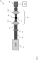
- Fig. 1 shows a schematic diagram of a sensor system 10 for sensing a physical quantity according to an embodiment.
- the sensor system 10 comprises: an excitation source 11 which is configured to generate an excitation signal 12; and a sensing volume 13 comprising one or more quantum systems, wherein the sensing volume is arranged to receive the excitation signal 12, wherein the excitation signal 12 induces an emission and/or an adaption of an optical signal 14 by the sensing volume 13, and wherein at least one characteristic of the optical signal depends on the physical quantity.
- the sensor system 10 further comprises an imaging system 15 which is configured to apply a transformation to the optical signal 14 (in particular, of an image pattern of the optical signal), thereby generating a transformed optical signal at an image plane 16; an spatially dependent attenuator 17 which is arranged at the image plane 16 and which is configured to attenuate the transformed optical signal; an optical sensor 18 which is configured to capture the thus attenuated optical signal and to detect a an image pattern of the (attenuated) optical signal; and a processor 19 which is configured to extract an information on the physical quantity from the detected image pattern.
- an imaging system 15 which is configured to apply a transformation to the optical signal 14 (in particular, of an image pattern of the optical signal), thereby generating a transformed optical signal at an image plane 16
- an spatially dependent attenuator 17 which is arranged at the image plane 16 and which is configured to attenuate the transformed optical signal
- an optical sensor 18 which is configured to capture the thus attenuated optical signal and to detect a an image pattern of the (attenuated
- the excitation source 11 is a laser which is configured to generate the excitation signal 12 in the form of a light beam.
- the sensing volume 13 can be a thin object that comprises one or multiple quantum systems, such as a diamond plate with one or more NV defects, or hot atoms in a thin atomic vapor cell.
- the sensing volume 13 can be comprised in a so-called sensing chip.
- the quantum volume is typically a gas which is stored in a vapor cell.
- the quantum system(s) in the sensing volume 13 can absorb light which passes through the sensing volume 13.
- a quantum sensor system based on such a "transmission setup" can, for example, be used in atomic clocks or DC magnetometers.
- the optical excitation signal 12 is directed through the sensing volume where it interacts with the quantum system, e.g. by locally exciting resonant transitions in atoms of the quantum system.
- the excitation signal 12 can be formed by a single laser beam which is used for excitation and detection.
- the excitation and detection signals can be separate signals which are generated by separate sources, wherein only the detection signal is captured by the optical sensor 18.
- the optical sensor can be any sensor which is able to resolve a spatial intensity distribution (i.e., an image pattern) of the optical signal (e.g., a camera, or an array of photodiodes).
- a spatial intensity distribution i.e., an image pattern
- the optical signal e.g., a camera, or an array of photodiodes.
- the imaging system 15 can be configured to image the optical signal 14 from the sensing volume 13 to the optical sensor.
- the imaging system comprises two lenses 15-1, 15-2.
- the attenuator 17 can be an optical filter.
- the optical filter is a spatial dependent filter which filters out DC and/or constant components from the optical signal.
- the imaging system 15 with the attenuator 17 can form a dark-field imaging system that only transmits non-DC components of the light and, thus, greatly reduces optical noise at the optical sensor 18.
- the image plane 16 can be a focal plane of the first lens 15-1.
- the optical filter can be a disk with a dark spot that blocks at least a portion of the light (e.g., a patch stop) or a line filter.
- the processor 19 can be a microprocessor or controller. For instance, the processor 19 analyses the image pattern of the attenuated optical signal to determine the physical quantity (e.g., by a comparison of the frequency distribution or parts thereof with a database of known distributions or by feeding the distribution to an algorithm).
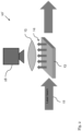
- Fig. 2 shows a sensor system 10' according to another embodiment.
- the optical signal 14 is a fluorescence signal which is generated in response to an excitation of the sensing volume 13 by the excitation signal 12.
- Such a setup can be referred to as fluorescence setup.
- the excitation signal 12 can be a laser signal, a microwave signal and/or a static electric and/or magnetic field.
- the sensing volume 13 may comprise a diamond solid comprising one or more NV defects.
- the quantum systems in the sensing volume 13 may emit fluorescence light based on interactions with the excitation signal.
- the z-dimension of the sensing volume 13 can be much thinner than the x- and y- dimensions.
- the sensing volume 13 may be thicker, but interactions only occur in a thin slice of quantum systems (e.g., excitation by a very elliptic laser beam).
- the system 10' shown in Fig. 2 may comprise the same or similar imaging system 15, spatially dependent attenuator 17 and processor 19 as the system 10 shown in Fig. 1 , which are, however, not shown in Fig. 2 for the sake of simplicity.
- sensors based on NV diamonds are read out by analyzing their emitted fluorescence light with an optical detector (as shown in Fig. 2 ), while sensors based on atomic vapor cells are read out via the transmitted power of a laser beam (as shown in Fig. 1 ).
- the response of NV centers can also be analyzed via a transmitted laser beam, and the response of atomic vapor cells can be analyzed via atom fluorescence.
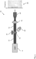
- Fig. 3 shows a schematic diagram of the sensor system 10 according to an embodiment.
- Fig. 3 shows a transmission analysis setup as shown in Fig. 1 .
- the imaging system 15 is depicted by single lens and the attenuator 17 and the processor 19 are not shown in Fig. 3 .
- the system 10 shown in Fig. 3 further comprises a field generator 31 which is configured to generate an electric and/or magnetic field within the sensing volume 13.
- the field generator 31 can comprise a magnet which forms an inhomogeneous magnetic field in the sensing volume 13, e.g. a vapor cell filled with gas.
- the system 10 may further comprise an element 32 configured to guide and/or focus the physical quantity or an electromagnetic (EM) signal representative of and/or based on the physical quantity towards the sensing volume 13.
- EM electromagnetic
- This element 32 can be an antenna and/or a waveguide.
- the antenna and/or waveguide guides an RF signal, e.g. a microwave signal, to be analyzed to the sensing volume 13.
- an RF signal e.g. a microwave signal
- the sensing volume 13 imprints a certain unique pattern on the optical signal 14, which can be analyzed with the camera.
- An example of a resulting image 33 having such an imprinted pattern is shown in Fig. 3 .
- the image 33 was generated based on a multicarrier signal to be measured.
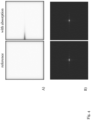
- Figs. 4A-B shows images recorded at different optical planes of the sensor system 10 according to an embodiment.
- the images were recorded with a transmission-based system, as shown in Fig. 1 and 3 , where the sensing volume comprises a gas in a vapor cell.
- Fig. 4A shows images of the optical signal 14 that were recorded without an attenuator 17. Thus, these images show the optical signal as it looks directly after the sensing volume 13. In the left image, no physical quantity or signal to be measured is present (reference image), while in the right image, a physical quantity or signal is present causing a visible absorption pattern.
- the sensing volume 13 e.g., the vapor cell
- the sensing volume 13 is mostly transparent to the laser light of the excitation signal 12, i.e. it has a very high transmission. This leads to a large optical signal on most pixels of the camera image (white area). If a signal to be measured is present (right image), a line-shaped pattern appears. This pattern is visible by the camera because the gas in the vapor cell absorbs some photons, so the photon count on some camera pixels is slightly reduced.
- the noise in particular, photon shot noise
- the measured signal can also strongly fluctuate with a standard deviation. In order to detect an absorption, it should be bigger than the shot noise.
- the sensor system 10 comprises the imaging system 15 and an attenuator which can be arranged as shown in Fig. 1 . These elements form a dark field imaging systems, which strongly reduces the optical noise.
- Fig. 4B shows images of the transformed optical signal 14 at the focal plane 16 of the imaging system 15 (as, e.g., shown in Fig. 1 ).
- the first lens 15-1 can transform the initial optical pattern of the optical signal 14 from the sensing volume 13 into the Fourier transformation of this pattern.
- the images in Fig. 4B are images in Fourier space of a reference measurement (left image) and a measurement with an absorption due to a physical quantity (right image).
- Fig. 5 shows an image recorded at the Fourier plane of the sensor system 10 as, e.g., shown in Fig. 1 or 3 , according to an embodiment.
- an optical attenuator 17 in the form of a line-shaped absorber or filter is arranged in the Fourier plane:
- the attenuator 17 is placed at the center of the Fourier image, because the center corresponds to low frequencies in the spectrum.
- This line-shaped absorber effectively absorbs DC frequency components of the initial image formed by the optical signal.
- the filter can filter out frequency components of the image because the lens system has Fourier transformed the image.
- Fig. 6 shows the resulting images of the attenuated optical signal (attenuated with the line-shaped absorber of Fig. 5 ) as captured by the optical sensor 18. Again, a reference image (left) with no absorption is compared to an image with an absorption due to the presence of a physical quantity to be analyzed (right image).
- the second lens 15-2 of the imaging system 15 performs an inverse Fourier transformation on the attenuated image in the Fourier plane (i.e., the image plane 16) and projects the resulting image on the optical sensor 18.
- the images show a mostly dark background (i.e., low photon count), because the DC components of the image are filtered out.
- the signal pattern of the absorption now adds photons to the background instead of removing photons.
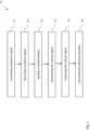
- Fig. 7 shows a flow diagram of a method 70 for sensing a physical quantity according to an embodiment. This method 70 can be carried out by any one of the sensor systems 10, 10' shown in Figs. 1-3 .
- the method 70 comprises the steps of: generating 71 an excitation signal 12; receiving 72 the excitation signal 12 at a sensing volume 13 which comprises one or more quantum systems; wherein the excitation signal 12 induces an emission and/or an adaption of an optical signal 14 by the sensing volume 13, and wherein at least one characteristic of the optical signal 14 depends on the physical quantity.
- the method 70 further comprises the steps of: applying 73 a transformation to the optical signal 14, thereby generating a transformed optical signal at an image plane16; spatially attenuating 74 the transformed optical signal at the image plane; capturing 75 the thus attenuated optical signal to detect an image pattern of the optical signal; and extracting 76 an information on the physical quantity from the image pattern.
- the step of spatially attenuating 74 the optical signal comprises filtering out DC or constant components from the optical signal.
- the transformation that is applied to the optical signal 14 can be a Fourier transformation. Subsequently, an inverse Fourier transformation is applied to the attenuated optical signal.
- the method may comprise the further step of: generating a magnetic and/or electric field in the sensing volume 13.
- the magnetic and/or electric field is in inhomogeneous magnetic and/or electric field, e.g. it has a field gradient in the sensing volume 13.
Landscapes
- Physics & Mathematics (AREA)
- General Physics & Mathematics (AREA)
- Engineering & Computer Science (AREA)
- Health & Medical Sciences (AREA)
- Theoretical Computer Science (AREA)
- General Health & Medical Sciences (AREA)
- Pathology (AREA)
- Immunology (AREA)
- Biochemistry (AREA)
- Analytical Chemistry (AREA)
- Chemical & Material Sciences (AREA)
- Life Sciences & Earth Sciences (AREA)
- Nuclear Medicine, Radiotherapy & Molecular Imaging (AREA)
- Spectroscopy & Molecular Physics (AREA)
- Computer Vision & Pattern Recognition (AREA)
- Multimedia (AREA)
- Software Systems (AREA)
- Medical Informatics (AREA)
- Evolutionary Computation (AREA)
- Databases & Information Systems (AREA)
- Computing Systems (AREA)
- Artificial Intelligence (AREA)
- Condensed Matter Physics & Semiconductors (AREA)
- Power Engineering (AREA)
- Investigating, Analyzing Materials By Fluorescence Or Luminescence (AREA)
Abstract
Description
- The disclosure relates to sensor systems, in particular a quantum sensor system, and to a corresponding method for sensing a physical quantity.
- Within the last years, there has been a lot of interest in sensing electromagnetic radiation (EM) or other physical quantities with quantum systems. The most common quantum systems include ground-state atoms, excited atoms (especially to Rydberg states), or atom-like systems. For instance, a quantum sensor, which employs such a quantum system, can detect EM radiation by an excitation of resonant transitions between two energy states in the quantum system.
- Often, the quantum systems are read out optically. However, this approach has the problem that the influence of the quantum system on the optical readout signal can be obscured by noise. For instance, the number of photons which are measured during readout can be subject to photon shot noise, i.e., the measured signal fluctuates with a standard deviation (the square root of the number of photons). For a high number of photons, this shot noise can be quite high. Furthermore, a large number of photons means that the detector can be easily saturated and, thus, a detector with large dynamic range may be required, which is more expensive or might not be available.
- Thus, there is a need to provide an improved system and method for sensing a physical quantity which avoid the above-mentioned disadvantages.
- This is achieved by the embodiments provided in the enclosed independent claims. Advantageous implementations of the present disclosure are further defined in the dependent claims.
- According to a first aspect, the present disclosure relates to a sensor system for sensing a physical quantity. The sensing system comprises: an excitation source which is configured to generate an excitation signal; a sensing volume comprising one or more quantum systems, wherein the sensing volume is arranged to receive the excitation signal, wherein the excitation signal induces an emission and/or an adaption of an optical signal by the sensing volume, wherein at least one characteristic of the optical signal depends on the physical quantity; an imaging system which is configured to apply a transformation to the optical signal, thereby generating a transformed optical signal at an image plane; an spatially dependent attenuator which is arranged at the image plane and which is configured to attenuate the transformed optical signal; an optical sensor which is configured to capture the thus attenuated optical signal and to detect an image pattern of the attenuated optical signal; and a processor which is configured to extract an information on the physical quantity from the captured image pattern.
- This achieves the advantage that, due to the attenuation of the transformed image, an optical noise in the detected readout signal can drastically be reduced. This can lead to a higher sensitivity of the sensor system. In addition, the photon counts on the pixels of the optical sensor can be reduced which, in turn, reduces the dynamic range requirements of the optical sensor. Thus, a simpler and potentially cheaper sensor can be used.
- The quantum system(s) can comprise ground state or excited atoms, e.g. Rydberg atoms, in a gas, or atom-like systems, such as NV defects in a diamond solid. The excitation signal can excite resonances in the quantum system(s).
- For example, the sensing volume and/or quantity to be measured may comprise an "inhomogeneity", such that the response of the sensor to the physical quantity is inhomogeneous as well (i.e., it contains a pattern that can be analyzed). This can be caused by the atoms at different positions in the sensing volume behaving differently (e.g. due to an inhomogeneous E/B-field), or if the signal to be measured is inhomogeneous (e.g. when it is coming from a focusing antenna or when measuring the field close to a waveguide).
- The excitation signal can be an optical signal (e.g., a laser beam) which optically excites the quantum system, e.g., to an excited quantum state. The excitation signal can further excite resonant transitions in the quantum system(s). In addition or alternatively, also off-resonant interactions can be excited by the excitation signal.
- The optical signal can be a luminescence or a fluorescence signal which is emitted in response to the excitation of the quantum system.
- For example, the optical signal corresponds to the excitation signal after transmitting (and thus interacting with) the sensing volume. In this example, the optical signal is directly based on the excitation signal.
- Alternatively, the excitation and detection signals can be separate signals from separate sources. For example, a strong laser is used for excitation (which prepares the quantum sensor to a certain initial state). However, this "excitation signal" is not read out by the camera. Instead, a weaker detection laser irradiates the sensing volume and is subsequently read out by the optical sensor, which is e.g. a camera.
- The sensing volume and, in particular, the quantum system can be exposed to the physical quantity. The physical quantity can be an E-field, a B-field, an EM field, a pressure or a temperature, or a parameter thereof (e.g., an amplitude or field strength). For instance, the quantum system can be arranged to receive at least a part of the physical quantity (e.g., an E-field, B-field or EM field).
- For example, the physical quantity (e.g., a static E or B field, temperature etc.) can shift or locally change energy levels and/or resonance frequencies of the atoms in the quantum system. This can affect the optical signal which can be locally modified due to the effect of the physical quantity on the quantum system. If the physical quantity is an electromagnetic (EM) signal, it may also cause resonant transitions in the quantum system, which may affect the optical readout signal.
- For example, EM-fields may also have an effect on the quantum system if they are non-resonant. These off-resonant interactions are typically weaker, but may also be utilized for sensing.
- The imaging system can be configured to image the optical signal on the optical sensor.
- The optical sensor can comprise a camera or an array of photodiodes.
- The image pattern of the (attenuated) optical signal, which is detected by the optical sensor, can be an intensity distribution or profile of the signal (i.e., the spatial profile of the optical signal). This distribution or profile can define an image that is captured at the optical sensor. The spatial profile of the optical signal can be correlated with frequency information of an EM wave to be measured. The exact image pattern that is captured can be caused by absorption and/or emission in the sensing volume.
- The processor can be configured to map the image pattern respectively intensity distribution/profile to an information about the physical quantity. For instance, the physical quantity imprints a unique pattern (e.g., an absorption pattern) in the intensity distribution of the optical signal, wherein the processor detects this pattern and correlates it with the physical quantity. Thus, a characteristic of the optical signal (the exact intensity and/or frequency distribution) depends on the physical quantity.
- The sensing volume can be a thin object which comprises one or more quantum systems, e.g. a sensing chip.
- In an implementation form, the spatially dependent attenuator is an optical filter, for instance a line filter.
- For instance, the attenuator can be a type of mask.
- For example, the filter is configured to filter out DC components from the image pattern of the optical signal, e.g. from an image formed by the optical signal.
- The sensor system can be a quantum sensor system.
- In an implementation form, the imaging system comprises a first lens which is configured to apply a Fourier transformation to the image pattern of the optical signal. Thus, the transformed image pattern of the optical signal can be a Fourier transformed pattern. For instance, due to this Fourier transformation, the attenuator can filter out frequency components of the image.
- For instance, the spatially dependent attenuator is arranged at the center of the Fourier image, because the center corresponds to low frequencies in the spectrum. Thus, the attenuator can effectively absorb the DC frequency components of the initial image formed by the optical signal.
- In an implementation form, the imaging system comprises a second lens which is configured to apply an inverse Fourier transformation to the image pattern of the attenuated optical signal.
- In an implementation form, the sensing volume comprises a diamond solid comprising one or more NV defects, wherein the optical signal is a fluorescence signal emitted by the sensing volume.
- In an implementation form, the sensing volume comprises a gas, in particular a quantum gas, wherein the optical signal passes through the gas and is at least partially absorbed by the gas. This absorption can be caused by induced resonant transitions. The physical quantity to be analyzed can thereby imprint a unique absorption pattern in the optical signal.
- In an implementation form, the sensor system further comprises a vapor cell configured to store the gas.
- In an implementation form, the sensor system further comprises a field generator configured to generate an electric and/or magnetic field within the sensing volume.
- The resonance frequency of the sensing volume, in particular of the quantum systems in the sensing volume, can be modified by the electric and/or magnetic field. For instance, the electric and/or magnetic field is inhomogeneous throughout the sensing volume and exhibits a local variation, e.g. a field gradient. As a consequence, a resonant frequency of the quantum system varies throughout the sensing volume which allows to detect the presence of different EM frequencies in the excitation signal and/or an EM signal to analyze.
- The field generator can comprise a magnet and/or capacitor plates.
- In an implementation form, the sensor system further comprises an element configured to guide and/or focus the physical quantity or an EM signal representative of the physical quantity towards the sensing volume.
- For example, the element can be an antenna or a waveguide.
- According to a second aspect, the present disclosure relates to a method for sensing a physical quantity. The method comprises the steps of: generating an excitation signal; receiving the excitation signal at a sensing volume which comprises one or more quantum systems; wherein the excitation signal induces an emission and/or an adaption of an optical signal by the sensing volume, wherein at least one characteristic of the optical signal depends on the physical quantity; applying a transformation to the optical signal, thereby generating a transformed optical signal at an image plane; spatially attenuating the transformed optical signal at the image plane; capturing the thus attenuated optical signal and detecting an image pattern of the attenuated optical signal; and extracting an information on the physical quantity from the captured image pattern.
- The method can be a method for quantum sensing a physical quantity.
- Hereby, spatially attenuating may refer to attenuating the optical signal with varying strength depending on spatial coordinates of the optical signal.
- In an implementation form, the step of spatially attenuating the optical signal comprises filtering out DC components from the image pattern of the optical signal.
- In an implementation form, the transformation that is applied to the optical signal is a Fourier transformation which is applied to the image pattern of the optical signal.
- In an implementation form, an inverse Fourier transformation is applied to the image pattern of the attenuated optical signal.
- In an implementation form, the method comprises the further step of: generating a magnetic and/or electric field in the sensing volume.
- The above description with regard to the sensor system according to the first aspect of the present disclosure is correspondingly valid for the method according to the second aspect of the present disclosure.
- In particular, the method according to the second aspect of the present disclosure can be carried out by the sensor system according to the first aspect of the present disclosure.
- The above-described aspects and implementation forms of the present disclosure will be explained in the following description of specific embodiments in relation to the enclosed drawings, in which:
-
Fig. 1 shows a schematic diagram of a sensor system for sensing a physical quantity according to an embodiment; -
Fig. 2 shows a schematic diagram of a sensor system for sensing a physical quantity according to an embodiment; -
Fig. 3 shows a schematic diagram of a sensor system for sensing a physical quantity according to an embodiment; -
Figs. 4A-B show images recorded at different optical planes of a sensor system according to an embodiment; -
Figs. 5 shows an image recorded at an optical plane of a sensor system according to an embodiment; -
Fig. 6 shows images recorded at an optical plane of a sensor system according to an embodiment; and -
Fig. 7 shows a flow diagram of a method for sensing a physical quantity according to an embodiment. -
Fig. 1 shows a schematic diagram of asensor system 10 for sensing a physical quantity according to an embodiment. - The
sensor system 10 comprises: anexcitation source 11 which is configured to generate anexcitation signal 12; and asensing volume 13 comprising one or more quantum systems, wherein the sensing volume is arranged to receive theexcitation signal 12, wherein theexcitation signal 12 induces an emission and/or an adaption of anoptical signal 14 by thesensing volume 13, and wherein at least one characteristic of the optical signal depends on the physical quantity. Thesensor system 10 further comprises animaging system 15 which is configured to apply a transformation to the optical signal 14 (in particular, of an image pattern of the optical signal), thereby generating a transformed optical signal at animage plane 16; an spatiallydependent attenuator 17 which is arranged at theimage plane 16 and which is configured to attenuate the transformed optical signal; anoptical sensor 18 which is configured to capture the thus attenuated optical signal and to detect a an image pattern of the (attenuated) optical signal; and aprocessor 19 which is configured to extract an information on the physical quantity from the detected image pattern. - For example, the
excitation source 11 is a laser which is configured to generate theexcitation signal 12 in the form of a light beam. - The
sensing volume 13 can be a thin object that comprises one or multiple quantum systems, such as a diamond plate with one or more NV defects, or hot atoms in a thin atomic vapor cell. Thesensing volume 13 can be comprised in a so-called sensing chip. - In a transition analysis setup, as e.g. shown in
Fig. 1 , the quantum volume is typically a gas which is stored in a vapor cell. In this example, the quantum system(s) in thesensing volume 13 can absorb light which passes through thesensing volume 13. A quantum sensor system based on such a "transmission setup" can, for example, be used in atomic clocks or DC magnetometers. - For example, the
optical excitation signal 12 is directed through the sensing volume where it interacts with the quantum system, e.g. by locally exciting resonant transitions in atoms of the quantum system. A part of the excitation signal, which is not absorbed in thesensing volume 13, exits the sensing volume and forms the optical signal which is subsequently imaged on theoptical sensor 18. In this case, theexcitation signal 12 can be formed by a single laser beam which is used for excitation and detection. - Alternatively, the excitation and detection signals can be separate signals which are generated by separate sources, wherein only the detection signal is captured by the
optical sensor 18. - The optical sensor can be any sensor which is able to resolve a spatial intensity distribution (i.e., an image pattern) of the optical signal (e.g., a camera, or an array of photodiodes).
- The
imaging system 15 can be configured to image theoptical signal 14 from thesensing volume 13 to the optical sensor. For instance, the imaging system comprises two lenses 15-1, 15-2. - The
attenuator 17 can be an optical filter. For instance, the optical filter is a spatial dependent filter which filters out DC and/or constant components from the optical signal. Thus, theimaging system 15 with theattenuator 17 can form a dark-field imaging system that only transmits non-DC components of the light and, thus, greatly reduces optical noise at theoptical sensor 18. - The
image plane 16 can be a focal plane of the first lens 15-1. - The optical filter can be a disk with a dark spot that blocks at least a portion of the light (e.g., a patch stop) or a line filter.
- The
processor 19 can be a microprocessor or controller. For instance, theprocessor 19 analyses the image pattern of the attenuated optical signal to determine the physical quantity (e.g., by a comparison of the frequency distribution or parts thereof with a database of known distributions or by feeding the distribution to an algorithm). -
Fig. 2 shows a sensor system 10' according to another embodiment. For instance, thereby theoptical signal 14 is a fluorescence signal which is generated in response to an excitation of thesensing volume 13 by theexcitation signal 12. Such a setup can be referred to as fluorescence setup. - The
excitation signal 12 can be a laser signal, a microwave signal and/or a static electric and/or magnetic field. - In this case, the
sensing volume 13 may comprise a diamond solid comprising one or more NV defects. The quantum systems in thesensing volume 13 may emit fluorescence light based on interactions with the excitation signal. - For instance, the z-dimension of the
sensing volume 13 can be much thinner than the x- and y- dimensions. Alternatively, thesensing volume 13 may be thicker, but interactions only occur in a thin slice of quantum systems (e.g., excitation by a very elliptic laser beam). - The system 10' shown in
Fig. 2 may comprise the same orsimilar imaging system 15, spatiallydependent attenuator 17 andprocessor 19 as thesystem 10 shown inFig. 1 , which are, however, not shown inFig. 2 for the sake of simplicity. - Typically, sensors based on NV diamonds are read out by analyzing their emitted fluorescence light with an optical detector (as shown in
Fig. 2 ), while sensors based on atomic vapor cells are read out via the transmitted power of a laser beam (as shown inFig. 1 ). However, in some cases, the response of NV centers can also be analyzed via a transmitted laser beam, and the response of atomic vapor cells can be analyzed via atom fluorescence. -
Fig. 3 shows a schematic diagram of thesensor system 10 according to an embodiment. In particular,Fig. 3 shows a transmission analysis setup as shown inFig. 1 . For the sake of simplicity, theimaging system 15 is depicted by single lens and theattenuator 17 and theprocessor 19 are not shown inFig. 3 . - The
system 10 shown inFig. 3 further comprises afield generator 31 which is configured to generate an electric and/or magnetic field within thesensing volume 13. For instance thefield generator 31 can comprise a magnet which forms an inhomogeneous magnetic field in thesensing volume 13, e.g. a vapor cell filled with gas. - The
system 10 may further comprise anelement 32 configured to guide and/or focus the physical quantity or an electromagnetic (EM) signal representative of and/or based on the physical quantity towards the sensingvolume 13. - This
element 32 can be an antenna and/or a waveguide. For instance, the antenna and/or waveguide guides an RF signal, e.g. a microwave signal, to be analyzed to thesensing volume 13. Depending on the frequency components of the applied RF signal, thesensing volume 13 imprints a certain unique pattern on theoptical signal 14, which can be analyzed with the camera. An example of a resultingimage 33 having such an imprinted pattern is shown inFig. 3 . Theimage 33 was generated based on a multicarrier signal to be measured. -
Figs. 4A-B shows images recorded at different optical planes of thesensor system 10 according to an embodiment. In particular, the images were recorded with a transmission-based system, as shown inFig. 1 and3 , where the sensing volume comprises a gas in a vapor cell. -
Fig. 4A shows images of theoptical signal 14 that were recorded without anattenuator 17. Thus, these images show the optical signal as it looks directly after thesensing volume 13. In the left image, no physical quantity or signal to be measured is present (reference image), while in the right image, a physical quantity or signal is present causing a visible absorption pattern. - Typically, the sensing volume 13 (e.g., the vapor cell) is mostly transparent to the laser light of the
excitation signal 12, i.e. it has a very high transmission. This leads to a large optical signal on most pixels of the camera image (white area). If a signal to be measured is present (right image), a line-shaped pattern appears. This pattern is visible by the camera because the gas in the vapor cell absorbs some photons, so the photon count on some camera pixels is slightly reduced. - However, due to the high number of photons that are transmitted by the vapor cell, the noise (in particular, photon shot noise) masks the influence of the physical quantity on the image (i.e., the visible absorption). The measured signal can also strongly fluctuate with a standard deviation. In order to detect an absorption, it should be bigger than the shot noise.
- Further, such high photon counts require an
optical sensor 18 with a high dynamic range. Most sensors have a saturation level, which is quickly reached. - These drawbacks, which occur if no imaging and attenuation is carried out, also apply when reading out a fluorescence signal from NV diamonds (e.g., with the setup shown in
Fig. 2 ). This is because, if there is only a laser and no other interaction, the NV centers emit strong fluorescence. When adding a field to be measured to the NV centers, their response is usually a slight reduction of the fluorescence signal. - To overcome these issues, the
sensor system 10 comprises theimaging system 15 and an attenuator which can be arranged as shown inFig. 1 . These elements form a dark field imaging systems, which strongly reduces the optical noise. -
Fig. 4B shows images of the transformedoptical signal 14 at thefocal plane 16 of the imaging system 15 (as, e.g., shown inFig. 1 ). In thefocal plane 16, the first lens 15-1 can transform the initial optical pattern of theoptical signal 14 from thesensing volume 13 into the Fourier transformation of this pattern. The images inFig. 4B are images in Fourier space of a reference measurement (left image) and a measurement with an absorption due to a physical quantity (right image). -
Fig. 5 shows an image recorded at the Fourier plane of thesensor system 10 as, e.g., shown inFig. 1 or3 , according to an embodiment. Thereby, anoptical attenuator 17 in the form of a line-shaped absorber or filter is arranged in the Fourier plane: - For instance, the
attenuator 17 is placed at the center of the Fourier image, because the center corresponds to low frequencies in the spectrum. This line-shaped absorber effectively absorbs DC frequency components of the initial image formed by the optical signal. Thereby, the filter can filter out frequency components of the image because the lens system has Fourier transformed the image. -
Fig. 6 shows the resulting images of the attenuated optical signal (attenuated with the line-shaped absorber ofFig. 5 ) as captured by theoptical sensor 18. Again, a reference image (left) with no absorption is compared to an image with an absorption due to the presence of a physical quantity to be analyzed (right image). - For instance, the second lens 15-2 of the
imaging system 15 performs an inverse Fourier transformation on the attenuated image in the Fourier plane (i.e., the image plane 16) and projects the resulting image on theoptical sensor 18. - Instead of a white background (i.e., high photon count) as shown in
Fig. 4A , the images show a mostly dark background (i.e., low photon count), because the DC components of the image are filtered out. The signal pattern of the absorption now adds photons to the background instead of removing photons. - This achieves the advantages that a higher sensitivity of the sensor can be achieved due to a drastically reduced photon shot noise of the background, and less photon counts are captured by the camera pixels, i.e., the demands on the dynamic range of the camera are reduced. This enables quantum sensing with higher sensitivity and dynamic range (e.g., in a quantum broadband receiver). For instance, an improvement of 10 dB can be expected.
-
Fig. 7 shows a flow diagram of amethod 70 for sensing a physical quantity according to an embodiment. Thismethod 70 can be carried out by any one of thesensor systems 10, 10' shown inFigs. 1-3 . - The
method 70 comprises the steps of: generating 71 anexcitation signal 12; receiving 72 theexcitation signal 12 at asensing volume 13 which comprises one or more quantum systems; wherein theexcitation signal 12 induces an emission and/or an adaption of anoptical signal 14 by thesensing volume 13, and wherein at least one characteristic of theoptical signal 14 depends on the physical quantity. Themethod 70 further comprises the steps of: applying 73 a transformation to theoptical signal 14, thereby generating a transformed optical signal at an image plane16; spatially attenuating 74 the transformed optical signal at the image plane; capturing 75 the thus attenuated optical signal to detect an image pattern of the optical signal; and extracting 76 an information on the physical quantity from the image pattern. - For instance, the step of spatially attenuating 74 the optical signal comprises filtering out DC or constant components from the optical signal.
- The transformation that is applied to the
optical signal 14 can be a Fourier transformation. Subsequently, an inverse Fourier transformation is applied to the attenuated optical signal. - The method may comprise the further step of: generating a magnetic and/or electric field in the
sensing volume 13. For instance, the magnetic and/or electric field is in inhomogeneous magnetic and/or electric field, e.g. it has a field gradient in thesensing volume 13. - All features described above or features shown in the figures can be combined with each other in any advantageous manner within the scope of the disclosure.
Claims (15)
- A sensor system for sensing a physical quantity, comprising:an excitation source (11) which is configured to generate an excitation signal (12);a sensing volume (13) comprising one or more quantum systems, wherein the sensing volume (13) is arranged to receive the excitation signal (12), wherein the excitation signal (12) induces an emission and/or an adaption of an optical signal (18) by the sensing volume (13), wherein at least one characteristic of the optical signal (18) depends on the physical quantity;an imaging system (15) which is configured to apply a transformation to the optical signal (18), thereby generating a transformed optical signal at an image plane (16);a spatially dependent attenuator (17) which is arranged at the image plane (16) and which is configured to attenuate the transformed optical signal (18);an optical sensor (18) which is configured to capture the thus attenuated optical signal and to detect an image pattern of the attenuated optical signal; anda processor (19) which is configured to extract an information on the physical quantity from the captured image pattern.
- The sensor system of claim 1,
wherein the spatially dependent attenuator is an optical filter, for instance a line filter. - The sensor system of claim 2,
wherein the optical filter is configured to filter out DC components from an image pattern of the optical signal. - The sensor system of any of the preceding claims,
wherein the imaging system comprises a first lens which is configured to apply a Fourier transformation to an image pattern of the optical signal. - The sensor system of claim 4,
wherein the imaging system comprises a second lens which is configured to apply an inverse Fourier transformation to the image pattern of the attenuated optical signal. - The sensor system of any of the preceding claims,
wherein the sensing volume comprises a diamond solid comprising one or more NV defects, wherein the optical signal is a fluorescence signal emitted by the sensing volume. - The sensor system any of the preceding claims,
wherein the sensing volume comprises a gas, in particular a quantum gas, wherein the optical signal passes through the gas and is at least partially absorbed by the gas. - The sensor system of claim 7, further comprising:
a vapor cell configured to store the gas. - The sensor system of any of the preceding claims, further comprising:
a field generator which is configured to generate an electric and/or magnetic field within the sensing volume. - The sensor system of any of the preceding claims, further comprising:
an element which is configured to guide and/or focus the physical quantity or an electromagnetic, EM, signal representative of the physical quantity towards the sensing volume. - A method for sensing a physical quantity, comprising the steps of:generating (11) an excitation signal;receiving the excitation signal at a sensing volume (13) which comprises one or more quantum systems; wherein the excitation signal induces an emission and/or an adaption of an optical signal (14) by the sensing volume (13), wherein at least one characteristic of the optical signal depends on the physical quantity;applying a transformation to the optical signal (14), thereby generating a transformed optical signal at an image plane (16);spatially attenuating the transformed optical signal at the image plane (16);capturing the thus attenuated optical signal and detecting an image pattern of the attenuated optical signal; andextracting an information on the physical quantity from the captured image pattern.
- The method of claim 11,
wherein the step of spatially attenuating the optical signal comprises filtering out DC components from the optical signal. - The method of claim 11 or 12,
wherein the transformation that is applied to the optical signal is a Fourier transformation which is applied to an image pattern of the optical signal. - The method of claim 13,
wherein an inverse Fourier transformation is applied to the image pattern of the attenuated optical signal. - The method of any of claims 11 to 14, further comprising the step of:
generating a magnetic and/or electric field in the sensing volume.
Applications Claiming Priority (1)
| Application Number | Priority Date | Filing Date | Title |
|---|---|---|---|
| US18/345,637 US12657662B2 (en) | 2023-06-30 | 2023-06-30 | Sensor system and method for sensing a physical quantity |
Publications (2)
| Publication Number | Publication Date |
|---|---|
| EP4484989A1 true EP4484989A1 (en) | 2025-01-01 |
| EP4484989B1 EP4484989B1 (en) | 2026-02-25 |
Family
ID=91034117
Family Applications (1)
| Application Number | Title | Priority Date | Filing Date |
|---|---|---|---|
| EP24174691.6A Active EP4484989B1 (en) | 2023-06-30 | 2024-05-08 | Sensor system and method for sensing a physical quantity |
Country Status (2)
| Country | Link |
|---|---|
| US (1) | US12657662B2 (en) |
| EP (1) | EP4484989B1 (en) |
Citations (1)
| Publication number | Priority date | Publication date | Assignee | Title |
|---|---|---|---|---|
| CN111175678A (en) * | 2020-03-10 | 2020-05-19 | 合肥工业大学 | Diamond vector magnetometer based on radial polarized light and application thereof |
Family Cites Families (9)
| Publication number | Priority date | Publication date | Assignee | Title |
|---|---|---|---|---|
| DE3138727A1 (en) | 1981-09-29 | 1983-04-21 | Siemens AG, 1000 Berlin und 8000 München | FREQUENCY ANALYZER IN PLANAR WAVE GUIDE TECHNOLOGY AND METHOD FOR PRODUCING A PLANAR GEODETIC LENS ON OR IN A SUBSTRATE |
| US9964925B2 (en) * | 2015-12-29 | 2018-05-08 | Oculus Vr, Llc | Holographic display architecture |
| US20190206070A1 (en) * | 2016-05-18 | 2019-07-04 | Auckland Uniservices Limited | Image registration method |
| EP3370486A1 (en) * | 2017-03-02 | 2018-09-05 | ASML Netherlands B.V. | Radiation source |
| CN115666377B (en) * | 2020-03-19 | 2025-09-02 | 斯坦福研究院 | Quantum electromagnetic field sensors and imagers |
| SE2051450A1 (en) * | 2020-12-11 | 2022-06-12 | Holtra Ab | Method and arrangement for holographic nanoparticle tracking analysis (H-NTA) in an off-axis digital holographic microscope |
| JPWO2023074750A1 (en) * | 2021-10-29 | 2023-05-04 | ||
| JP7845055B2 (en) * | 2022-05-31 | 2026-04-14 | 日本電気株式会社 | Atomic oscillator |
| EP4735853A1 (en) * | 2023-06-27 | 2026-05-06 | Quantum Valley Ideas Laboratories | Measuring thermal radiation using vapor cell sensors |
-
2023
- 2023-06-30 US US18/345,637 patent/US12657662B2/en active Active
-
2024
- 2024-05-08 EP EP24174691.6A patent/EP4484989B1/en active Active
Patent Citations (1)
| Publication number | Priority date | Publication date | Assignee | Title |
|---|---|---|---|---|
| CN111175678A (en) * | 2020-03-10 | 2020-05-19 | 合肥工业大学 | Diamond vector magnetometer based on radial polarized light and application thereof |
Non-Patent Citations (2)
| Title |
|---|
| AJOY A ET AL: "DC Magnetometry at the T_2 Limit", ARXIV.ORG, CORNELL UNIVERSITY LIBRARY, 201 OLIN LIBRARY CORNELL UNIVERSITY ITHACA, NY 14853, 15 November 2016 (2016-11-15), XP081902600, DOI: 10.1103/PHYSREVLETT.122.100501 * |
| HOSSEIN BABASHAH ET AL: "Optically detected magnetic resonance with an open source platform", ARXIV.ORG, CORNELL UNIVERSITY LIBRARY, 201 OLIN LIBRARY CORNELL UNIVERSITY ITHACA, NY 14853, 29 April 2022 (2022-04-29), XP091211346 * |
Also Published As
| Publication number | Publication date |
|---|---|
| EP4484989B1 (en) | 2026-02-25 |
| US20250005711A1 (en) | 2025-01-02 |
| US12657662B2 (en) | 2026-06-16 |
Similar Documents
| Publication | Publication Date | Title |
|---|---|---|
| CN112683332B (en) | Multi-physical-parameter wide-field quantum camera based on ensemble nitrogen atom-vacancy color center | |
| CN114858314B (en) | Diamond stress measurement system and method based on NV color center | |
| EP3809145B1 (en) | System for analyzing electromagnetic radiation | |
| WO2012008836A2 (en) | Inspection apparatus and replaceable door for a vacuum chamber of such an inspection apparatus and a method for operating an inspection apparatus | |
| US20140211199A1 (en) | Multiple concurrent spectral analyses | |
| JP4960255B2 (en) | Gamma ray imaging device | |
| KR102274933B1 (en) | Diamond nitrogen vacancy center magnetic field sensor | |
| US7038220B2 (en) | Dose distribution reading method and reader for glass dosimeter | |
| CN114113151B (en) | Coupled magnetic imaging device and measurement method | |
| CN114994112A (en) | Monochromatic focusing polarized X-ray optical system and method of use and fluorescence spectrometer | |
| US20250005711A1 (en) | Sensor system and method for sensing a physical quantity | |
| CN115003981A (en) | Method and system for combining OCD and light reflection | |
| EP3881055B1 (en) | Systems and method for correcting transmission deviations of interference filters due to angle of incidence | |
| CN116539089B (en) | An in-situ testing system | |
| CN106841013A (en) | A kind of method that microscopic organism is distinguished based on Quantum Correlation imaging technique | |
| JP4977068B2 (en) | Image acquisition device and sample inspection device | |
| CN116413225A (en) | Spectral analysis method, device, electronic equipment and storage medium | |
| CN117269126A (en) | An event-guided highly targeted fluorescence correlation spectroscopy method and its device | |
| JPH04295782A (en) | Surface analyzer, surface analyzing method and measuring device for magnetic resonance phenomenon | |
| JP3014225B2 (en) | Radiation dose reader | |
| US12504456B2 (en) | Quantum sensor system for sensing electromagnetic radiation | |
| CN119023703B (en) | Nondestructive testing method and nondestructive testing device | |
| US20240192294A1 (en) | Digital lock-in for magnetic imaging with nitrogen vacancy centers in diamonds | |
| CN114076748B (en) | ODMR spectrometer nitrogen-vacancy color center identification method and system | |
| WO2025033337A1 (en) | Compound-eye optical system quantum measurement |
Legal Events
| Date | Code | Title | Description |
|---|---|---|---|
| PUAI | Public reference made under article 153(3) epc to a published international application that has entered the european phase |
Free format text: ORIGINAL CODE: 0009012 |
|
| STAA | Information on the status of an ep patent application or granted ep patent |
Free format text: STATUS: THE APPLICATION HAS BEEN PUBLISHED |
|
| AK | Designated contracting states |
Kind code of ref document: A1 Designated state(s): AL AT BE BG CH CY CZ DE DK EE ES FI FR GB GR HR HU IE IS IT LI LT LU LV MC ME MK MT NL NO PL PT RO RS SE SI SK SM TR |
|
| STAA | Information on the status of an ep patent application or granted ep patent |
Free format text: STATUS: REQUEST FOR EXAMINATION WAS MADE |
|
| 17P | Request for examination filed |
Effective date: 20250227 |
|
| GRAP | Despatch of communication of intention to grant a patent |
Free format text: ORIGINAL CODE: EPIDOSNIGR1 |
|
| STAA | Information on the status of an ep patent application or granted ep patent |
Free format text: STATUS: GRANT OF PATENT IS INTENDED |
|
| INTG | Intention to grant announced |
Effective date: 20251201 |
|
| GRAS | Grant fee paid |
Free format text: ORIGINAL CODE: EPIDOSNIGR3 |
|
| GRAA | (expected) grant |
Free format text: ORIGINAL CODE: 0009210 |
|
| STAA | Information on the status of an ep patent application or granted ep patent |
Free format text: STATUS: THE PATENT HAS BEEN GRANTED |
|
| P01 | Opt-out of the competence of the unified patent court (upc) registered |
Free format text: CASE NUMBER: UPC_APP_0019624_4484989/2025 Effective date: 20251230 |
|
| AK | Designated contracting states |
Kind code of ref document: B1 Designated state(s): AL AT BE BG CY CZ DE DK EE ES FI FR GB GR HR HU IS IT LT LU LV MC ME MK MT NL NO PL PT RO RS SE SI SK SM TR |
|
| RBV | Designated contracting states (corrected) |
Designated state(s): AL AT BE BG CY CZ DE DK EE ES FI FR GB GR HR HU IS IT LT LU LV MC ME MK MT NL NO PL PT RO RS SE SI SK SM TR |
|
| REG | Reference to a national code |
Ref country code: GB Ref legal event code: FG4D |
|
| REG | Reference to a national code |
Ref country code: DE Ref legal event code: R096 Ref document number: 602024002744 Country of ref document: DE |
|
| REG | Reference to a national code |
Ref country code: NL Ref legal event code: MP Effective date: 20260225 |
|
| PG25 | Lapsed in a contracting state [announced via postgrant information from national office to epo] |
Ref country code: RS Free format text: LAPSE BECAUSE OF FAILURE TO SUBMIT A TRANSLATION OF THE DESCRIPTION OR TO PAY THE FEE WITHIN THE PRESCRIBED TIME-LIMIT Effective date: 20260525 |
|
| PG25 | Lapsed in a contracting state [announced via postgrant information from national office to epo] |
Ref country code: ES Free format text: LAPSE BECAUSE OF FAILURE TO SUBMIT A TRANSLATION OF THE DESCRIPTION OR TO PAY THE FEE WITHIN THE PRESCRIBED TIME-LIMIT Effective date: 20260225 |
|
| PG25 | Lapsed in a contracting state [announced via postgrant information from national office to epo] |
Ref country code: PL Free format text: LAPSE BECAUSE OF FAILURE TO SUBMIT A TRANSLATION OF THE DESCRIPTION OR TO PAY THE FEE WITHIN THE PRESCRIBED TIME-LIMIT Effective date: 20260225 |
|
| PG25 | Lapsed in a contracting state [announced via postgrant information from national office to epo] |
Ref country code: GR Free format text: LAPSE BECAUSE OF FAILURE TO SUBMIT A TRANSLATION OF THE DESCRIPTION OR TO PAY THE FEE WITHIN THE PRESCRIBED TIME-LIMIT Effective date: 20260526 |
|
| REG | Reference to a national code |
Ref country code: LT Ref legal event code: MG9D |
|
| PG25 | Lapsed in a contracting state [announced via postgrant information from national office to epo] |
Ref country code: LT Free format text: LAPSE BECAUSE OF FAILURE TO SUBMIT A TRANSLATION OF THE DESCRIPTION OR TO PAY THE FEE WITHIN THE PRESCRIBED TIME-LIMIT Effective date: 20260225 |
|
| PGFP | Annual fee paid to national office [announced via postgrant information from national office to epo] |
Ref country code: DE Payment date: 20260520 Year of fee payment: 3 |
|
| PG25 | Lapsed in a contracting state [announced via postgrant information from national office to epo] |
Ref country code: NO Free format text: LAPSE BECAUSE OF FAILURE TO SUBMIT A TRANSLATION OF THE DESCRIPTION OR TO PAY THE FEE WITHIN THE PRESCRIBED TIME-LIMIT Effective date: 20260525 |
|
| PG25 | Lapsed in a contracting state [announced via postgrant information from national office to epo] |
Ref country code: SE Free format text: LAPSE BECAUSE OF FAILURE TO SUBMIT A TRANSLATION OF THE DESCRIPTION OR TO PAY THE FEE WITHIN THE PRESCRIBED TIME-LIMIT Effective date: 20260225 Ref country code: AT Free format text: LAPSE BECAUSE OF FAILURE TO SUBMIT A TRANSLATION OF THE DESCRIPTION OR TO PAY THE FEE WITHIN THE PRESCRIBED TIME-LIMIT Effective date: 20260225 Ref country code: FI Free format text: LAPSE BECAUSE OF FAILURE TO SUBMIT A TRANSLATION OF THE DESCRIPTION OR TO PAY THE FEE WITHIN THE PRESCRIBED TIME-LIMIT Effective date: 20260225 |
|
| REG | Reference to a national code |
Ref country code: AT Ref legal event code: MK05 Ref document number: 1891403 Country of ref document: AT Kind code of ref document: T Effective date: 20260225 |
|
| PG25 | Lapsed in a contracting state [announced via postgrant information from national office to epo] |
Ref country code: HR Free format text: LAPSE BECAUSE OF FAILURE TO SUBMIT A TRANSLATION OF THE DESCRIPTION OR TO PAY THE FEE WITHIN THE PRESCRIBED TIME-LIMIT Effective date: 20260225 |
|
| PG25 | Lapsed in a contracting state [announced via postgrant information from national office to epo] |
Ref country code: PT Free format text: LAPSE BECAUSE OF FAILURE TO SUBMIT A TRANSLATION OF THE DESCRIPTION OR TO PAY THE FEE WITHIN THE PRESCRIBED TIME-LIMIT Effective date: 20260625 Ref country code: IS Free format text: LAPSE BECAUSE OF FAILURE TO SUBMIT A TRANSLATION OF THE DESCRIPTION OR TO PAY THE FEE WITHIN THE PRESCRIBED TIME-LIMIT Effective date: 20260625 |
|
| PG25 | Lapsed in a contracting state [announced via postgrant information from national office to epo] |
Ref country code: NL Free format text: LAPSE BECAUSE OF FAILURE TO SUBMIT A TRANSLATION OF THE DESCRIPTION OR TO PAY THE FEE WITHIN THE PRESCRIBED TIME-LIMIT Effective date: 20260225 |
|
| PGFP | Annual fee paid to national office [announced via postgrant information from national office to epo] |
Ref country code: FR Payment date: 20260522 Year of fee payment: 3 |
|
| PG25 | Lapsed in a contracting state [announced via postgrant information from national office to epo] |
Ref country code: LV Free format text: LAPSE BECAUSE OF FAILURE TO SUBMIT A TRANSLATION OF THE DESCRIPTION OR TO PAY THE FEE WITHIN THE PRESCRIBED TIME-LIMIT Effective date: 20260225 |
|
| PG25 | Lapsed in a contracting state [announced via postgrant information from national office to epo] |
Ref country code: BG Free format text: LAPSE BECAUSE OF FAILURE TO SUBMIT A TRANSLATION OF THE DESCRIPTION OR TO PAY THE FEE WITHIN THE PRESCRIBED TIME-LIMIT Effective date: 20260225 |