EP4478423A1 - Transistorstruktur mit vertikalem kanal und herstellungsverfahren dafür - Google Patents
Transistorstruktur mit vertikalem kanal und herstellungsverfahren dafür Download PDFInfo
- Publication number
- EP4478423A1 EP4478423A1 EP23769425.2A EP23769425A EP4478423A1 EP 4478423 A1 EP4478423 A1 EP 4478423A1 EP 23769425 A EP23769425 A EP 23769425A EP 4478423 A1 EP4478423 A1 EP 4478423A1
- Authority
- EP
- European Patent Office
- Prior art keywords
- layer
- contact
- contact layer
- semiconductor
- semiconductor channel
- Prior art date
- Legal status (The legal status is an assumption and is not a legal conclusion. Google has not performed a legal analysis and makes no representation as to the accuracy of the status listed.)
- Pending
Links
Images


Classifications
-
- H—ELECTRICITY
- H10—SEMICONDUCTOR DEVICES; ELECTRIC SOLID-STATE DEVICES NOT OTHERWISE PROVIDED FOR
- H10D—INORGANIC ELECTRIC SEMICONDUCTOR DEVICES
- H10D30/00—Field-effect transistors [FET]
- H10D30/60—Insulated-gate field-effect transistors [IGFET]
- H10D30/63—Vertical IGFETs
-
- H—ELECTRICITY
- H10—SEMICONDUCTOR DEVICES; ELECTRIC SOLID-STATE DEVICES NOT OTHERWISE PROVIDED FOR
- H10D—INORGANIC ELECTRIC SEMICONDUCTOR DEVICES
- H10D30/00—Field-effect transistors [FET]
- H10D30/01—Manufacture or treatment
- H10D30/021—Manufacture or treatment of FETs having insulated gates [IGFET]
- H10D30/031—Manufacture or treatment of FETs having insulated gates [IGFET] of thin-film transistors [TFT]
-
- H—ELECTRICITY
- H10—SEMICONDUCTOR DEVICES; ELECTRIC SOLID-STATE DEVICES NOT OTHERWISE PROVIDED FOR
- H10B—ELECTRONIC MEMORY DEVICES
- H10B63/00—Resistance change memory devices, e.g. resistive RAM [ReRAM] devices
- H10B63/30—Resistance change memory devices, e.g. resistive RAM [ReRAM] devices comprising selection components having three or more electrodes, e.g. transistors
- H10B63/34—Resistance change memory devices, e.g. resistive RAM [ReRAM] devices comprising selection components having three or more electrodes, e.g. transistors of the vertical channel field-effect transistor type
-
- H—ELECTRICITY
- H10—SEMICONDUCTOR DEVICES; ELECTRIC SOLID-STATE DEVICES NOT OTHERWISE PROVIDED FOR
- H10B—ELECTRONIC MEMORY DEVICES
- H10B63/00—Resistance change memory devices, e.g. resistive RAM [ReRAM] devices
- H10B63/80—Arrangements comprising multiple bistable or multi-stable switching components of the same type on a plane parallel to the substrate, e.g. cross-point arrays
- H10B63/84—Arrangements comprising multiple bistable or multi-stable switching components of the same type on a plane parallel to the substrate, e.g. cross-point arrays arranged in a direction perpendicular to the substrate, e.g. 3D cell arrays
- H10B63/845—Arrangements comprising multiple bistable or multi-stable switching components of the same type on a plane parallel to the substrate, e.g. cross-point arrays arranged in a direction perpendicular to the substrate, e.g. 3D cell arrays the switching components being connected to a common vertical conductor
-
- H—ELECTRICITY
- H10—SEMICONDUCTOR DEVICES; ELECTRIC SOLID-STATE DEVICES NOT OTHERWISE PROVIDED FOR
- H10D—INORGANIC ELECTRIC SEMICONDUCTOR DEVICES
- H10D30/00—Field-effect transistors [FET]
- H10D30/01—Manufacture or treatment
- H10D30/021—Manufacture or treatment of FETs having insulated gates [IGFET]
- H10D30/025—Manufacture or treatment of FETs having insulated gates [IGFET] of vertical IGFETs
-
- H—ELECTRICITY
- H10—SEMICONDUCTOR DEVICES; ELECTRIC SOLID-STATE DEVICES NOT OTHERWISE PROVIDED FOR
- H10D—INORGANIC ELECTRIC SEMICONDUCTOR DEVICES
- H10D30/00—Field-effect transistors [FET]
- H10D30/60—Insulated-gate field-effect transistors [IGFET]
- H10D30/67—Thin-film transistors [TFT]
- H10D30/6728—Vertical TFTs
-
- H—ELECTRICITY
- H10—SEMICONDUCTOR DEVICES; ELECTRIC SOLID-STATE DEVICES NOT OTHERWISE PROVIDED FOR
- H10D—INORGANIC ELECTRIC SEMICONDUCTOR DEVICES
- H10D30/00—Field-effect transistors [FET]
- H10D30/60—Insulated-gate field-effect transistors [IGFET]
- H10D30/67—Thin-film transistors [TFT]
- H10D30/674—Thin-film transistors [TFT] characterised by the active materials
- H10D30/6755—Oxide semiconductors, e.g. zinc oxide, copper aluminium oxide or cadmium stannate
-
- H—ELECTRICITY
- H10—SEMICONDUCTOR DEVICES; ELECTRIC SOLID-STATE DEVICES NOT OTHERWISE PROVIDED FOR
- H10D—INORGANIC ELECTRIC SEMICONDUCTOR DEVICES
- H10D62/00—Semiconductor bodies, or regions thereof, of devices having potential barriers
- H10D62/80—Semiconductor bodies, or regions thereof, of devices having potential barriers characterised by the materials
- H10D62/83—Semiconductor bodies, or regions thereof, of devices having potential barriers characterised by the materials being Group IV materials, e.g. B-doped Si or undoped Ge
-
- H—ELECTRICITY
- H10—SEMICONDUCTOR DEVICES; ELECTRIC SOLID-STATE DEVICES NOT OTHERWISE PROVIDED FOR
- H10D—INORGANIC ELECTRIC SEMICONDUCTOR DEVICES
- H10D64/00—Electrodes of devices having potential barriers
- H10D64/60—Electrodes characterised by their materials
- H10D64/62—Electrodes ohmically coupled to a semiconductor
-
- H—ELECTRICITY
- H10—SEMICONDUCTOR DEVICES; ELECTRIC SOLID-STATE DEVICES NOT OTHERWISE PROVIDED FOR
- H10D—INORGANIC ELECTRIC SEMICONDUCTOR DEVICES
- H10D30/00—Field-effect transistors [FET]
- H10D30/40—FETs having zero-dimensional [0D], one-dimensional [1D] or two-dimensional [2D] charge carrier gas channels
- H10D30/47—FETs having zero-dimensional [0D], one-dimensional [1D] or two-dimensional [2D] charge carrier gas channels having two-dimensional [2D] charge carrier gas channels, e.g. nanoribbon FETs or high electron mobility transistors [HEMT]
- H10D30/481—FETs having two-dimensional material channels, e.g. transition metal dichalcogenide [TMD] FETs
- H10D30/485—Vertical FETs having two-dimensional material channels
-
- H—ELECTRICITY
- H10—SEMICONDUCTOR DEVICES; ELECTRIC SOLID-STATE DEVICES NOT OTHERWISE PROVIDED FOR
- H10D—INORGANIC ELECTRIC SEMICONDUCTOR DEVICES
- H10D62/00—Semiconductor bodies, or regions thereof, of devices having potential barriers
- H10D62/80—Semiconductor bodies, or regions thereof, of devices having potential barriers characterised by the materials
- H10D62/881—Semiconductor bodies, or regions thereof, of devices having potential barriers characterised by the materials being a two-dimensional material
- H10D62/883—Transition metal dichalcogenides, e.g. MoSe2
Definitions
- This application relates to the field of semiconductor technologies, and in particular, to a vertical channel transistor and a manufacturing method.
- a transistor with a vertical channel becomes one of mainstream choices, to increase density of a storage array and reduce costs.
- the vertical channel transistor has a natural short-channel characteristic, and a semiconductor channel is located between a bottom electrode and a top electrode in a sandwich structure. Therefore, research and development of the vertical transistor are expected to be a new direction of device miniaturization. This can reduce a channel length to below 10 nm or even 5 nm.
- Embodiments of this application provide a vertical channel transistor structure and a manufacturing method, to effectively reduce a contact resistance of a vertical channel transistor.
- a first aspect of this application provides a vertical channel transistor structure.
- the structure includes a stacked structure, where the stacked structure includes a first metal layer, a first contact layer, an insulation dielectric layer, a second contact layer, and a second metal layer, the first contact layer is located between the first metal layer and the insulation dielectric layer, and the second contact layer is located between the second metal layer and the insulation dielectric layer.
- the stacked structure is provided with a groove, the groove penetrates the second metal layer, the second contact layer, the insulation dielectric layer, and the second contact layer, and the first groove is at least partially recessed into the first metal layer.
- a semiconductor channel layer, a gate oxygen dielectric layer, and a gate are disposed in the groove.
- Materials of the first contact layer and the second contact layer are conductor materials or semiconductor materials whose conductivities are higher than that of the semiconductor channel layer.
- the semiconductor channel layer is separately in contact with the first metal layer and the second metal layer in the groove, and the gate oxygen dielectric layer is disposed between the semiconductor channel layer and the gate.
- one of the first metal layer and the second metal layer is a source, and the other is a drain.
- a contact surface between the source and the semiconductor channel layer and a contact surface between the semiconductor channel layer and the drain Both contact between the source and the semiconductor channel layer and contact between the semiconductor channel layer and the drain are usually Schottky contact in the vertical device structure, and a thermal excitation mode is used for current injection.
- a contact resistance is large, electronic potential energy required for passing through a barrier is large, and a current is small.
- contact layers are respectively disposed between the drain and the insulation dielectric layer and between the source and the insulation dielectric layer.
- Electrons need to pass through four contact surfaces in total from the source to the drain: a contact surface between the source and the first contact layer, a contact surface between the first contact layer and the semiconductor channel layer, a contact surface between the semiconductor channel layer and the second contact layer, and a contact surface between the second contact layer and the drain.
- the materials of the two contact layers are the conductor materials or the semiconductor materials whose conductivities are higher than that of the semiconductor channel layer, and the conductor materials used by the contact layers are different from metal of the source metal layer and metal of the drain metal layer, and can separately form good contact with the semiconductor channel layer, a contact resistance of the contact surface between the contact layer and the semiconductor channel layer is far less than a contact resistance of a contact surface between the source and the semiconductor channel layer and a contact resistance of a contact surface between the drain and the semiconductor channel layer.
- the contact layer is in good contact with the metal, a contact resistance formed between the source and the contact layer and a contact resistance between the drain and the contact layer are also extremely small.
- a sum of a resistance of the contact surface between the source and the contact layer and a resistance of the contact surface between the contact layer and the semiconductor channel layer is less than a resistance of the contact surface between the source and the semiconductor channel layer in the conventional technology.
- a sum of a resistance of the contact surface between the drain and the contact layer and a resistance of the contact surface between the contact layer and the semiconductor channel layer is less than a resistance of the contact surface between the drain and the semiconductor channel layer in the conventional technology.
- the contact resistance formed between the source and the contact layer and the contact resistance formed between the drain and the contact layer can be ignored.
- a total resistance of the four contact surfaces through which the electrons pass from the source to the drain is less than a total resistance of the two contact surfaces through which the electrons pass from the source to the drain in the conventional technology, so that ohmic contact (which may also be referred to as ohmic-like contact) can be formed between the source and the semiconductor channel layer and between the drain and the semiconductor channel layer.
- ohmic contact which may also be referred to as ohmic-like contact
- a contact resistance of the vertical channel transistor is greatly reduced, and a current flowing from the source to the drain is increased, that is, an operating current of the vertical channel transistor is increased.
- the contact resistance of the device can be reduced because a contact area between the semiconductor and the source/drain is increased.
- the contact area between a channel and the source/drain in a condition that a horizontal area of the transistor device is not increased, the contact area between a channel and the source/drain can be increased, to effectively reduce the contact resistance, and a threshold of a channel material is kept unchanged, to improve device performance.
- this solution of this application is widely applicable, and may be used to optimize a contact resistance of a transistor made of any material.
- the contact resistance of the transistor (which may also be referred to as a source-drain contact resistance) may be understood as a sum of Rs and Rd.
- the contact resistance of the transistor is less than a specific threshold, it is considered that ohmic contact is formed in the transistor.
- the transistor with the ohmic contact has a small contact resistance and a large operating current. It should be understood that the contact resistance and the sum of Rs and Rd may be only approximate, but not necessarily strictly equal.
- the groove is the first groove
- the semiconductor channel layer covers a bottom and a side wall of the first groove to form a second groove
- the gate oxygen dielectric layer covers a bottom and a side wall of the second groove to form a third groove
- the gate is disposed in the third groove.
- the semiconductor channel layer, the gate oxygen dielectric layer, and the gate are sequentially disposed on a bottom surface of the groove; and the semiconductor channel layer, the gate oxygen dielectric layer, and the gate are sequentially disposed from outside to inside on the side wall of the groove.
- the resistance of the contact surface formed between the first contact layer and the semiconductor channel layer and the resistance of the contact surface formed between the second contact layer and the semiconductor channel layer are respectively less than a resistance of a contact surface formed between the first metal layer and the semiconductor channel layer and a resistance of a contact surface formed between the second metal layer and the semiconductor channel layer.
- a sum of a resistance of a contact surface formed between the first contact layer and the first metal layer and a resistance of a contact surface formed between the first contact layer and the semiconductor channel layer is less than a resistance of a contact surface formed between the first metal layer and the semiconductor channel layer; and a sum of a resistance of a contact surface formed between the second contact layer and the second metal layer and a resistance of a contact surface formed between the second contact layer and the semiconductor channel layer is less than a resistance of a contact surface formed between the second metal layer and the semiconductor channel layer.
- the resistance of the contact surface formed between the first contact layer and the first metal layer and the resistance of the contact surface formed between the second contact layer and the second metal layer are less than a first threshold.
- the first threshold is close to 0. Therefore, the resistance of the contact surface formed between the contact layer and the metal layer may be ignored.
- the materials of the first contact layer and the second contact layer are the conductor materials
- the semiconductor channel layer is an N-type semiconductor
- the materials of the first contact layer and the second contact layer are first conductor materials, where a work function of the first conductor material is less than or close to electron affinity of the semiconductor channel layer; or if the semiconductor channel layer is a P-type semiconductor, the materials of the first contact layer and the second contact layer are second conductor materials, where a work function of the second conductor material is greater than or close to a sum of electron affinity and a band gap of the semiconductor channel layer.
- the materials of the first contact layer and the second contact layer are the semiconductor materials
- the materials of the first contact layer and the second contact layer are first semiconductor materials, where a conduction band location of the first semiconductor material is close to a conduction band location of the first N-type semiconductor, and a conductivity of the first semiconductor material is greater than or equal to a conductivity of the first N-type semiconductor; or if the semiconductor channel layer is a first P-type semiconductor, the materials of the first contact layer and the second contact layer are second semiconductor materials, where a valence band location of the second conductor material is close to a valence band location of the first P-type semiconductor, and a conductivity of the second conductor material is greater than or equal to a conductivity of the first P-type semiconductor.
- the vertical channel transistor provided in embodiments of this application may be a vertical channel thin film transistor (Thin Film Transistor, TFT).
- first contact layer and the second contact layer each may also be referred to as a transition layer, an ohmic contact layer, or an ohmic contact intercalation layer.
- the conductor materials of the first contact layer and the second contact layer include titanium Ti, gold Au, tungsten W, molybdenum Mo, aluminum Al, or titanium nitride TiN.
- the semiconductor materials used by the first contact layer and the second contact layer include indium gallium zinc oxide InGaZnO, indium zinc oxide InZnO, indium tin oxide InSnO, indium oxide In2O3, gallium oxide Ga2O3, indium titanium oxide InTiO, or zinc oxide ZnO.
- the materials used by the first contact layer and the second contact layer further include heavily doped P-type silicon Si and N-type Si, or any combination of the P-type silicon Si and the N-type Si.
- the first contact layer and the second contact layer are doped semiconductor layers, and a material of the doped semiconductor layer is obtained by doping a material of the semiconductor channel layer.
- the contact layer may use a same semiconductor as the semiconductor channel, but the semiconductor at the contact layer needs to be doped or processed in another way, so that the contact layer has a lower resistance.
- the first contact layer and the second contact layer are semiconductors
- the first contact layer and the second contact layer may also be referred to as the doped semiconductor layers, and a resistance of the doped semiconductor layer is lower than a resistance of the semiconductor channel layer.
- the first contact layer, the second contact layer, and the semiconductor channel layer are all P-type semiconductors or N-type semiconductors; the first contact layer and the second contact layer are N-type semiconductors, and the semiconductor channel layer is a P-type semiconductor; or the first contact layer and the second contact layer are P-type semiconductors, and the semiconductor channel layer is an N-type semiconductor.
- the ohmic contact may be formed between the source/drain and the semiconductor channel layer after the ohmic contact layer is introduced. If a material of an ohmic contact layer and a material of the semiconductor channel layer have inconsistent polarities, doping concentration of the ohmic contact layer needs to be increased, to form PN junction ohmic contact between the source/drain and the semiconductor channel layer. This expands selection of a device material, this solution can be widely used to optimize a contact resistance of a device made of any material, and this implements a heterogeneous-contact transistor device.
- the structure is in a cylindrical shape.
- the stacked structure surrounds the semiconductor channel layer, and the semiconductor channel layer is completely located in the vertical groove inside the stacked structure.
- This implementation is a channel-all-around (Channel-All-Around, CAA) manner.
- the structure is in a square columnar shape.
- the stacked structure includes a first stacked substructure and a second stacked substructure, the semiconductor channel layer includes a first semiconductor channel layer and a second semiconductor channel layer, and the gate oxygen dielectric layer includes a first gate oxygen dielectric layer and a second gate oxygen dielectric layer.
- the gate is disposed between the first stacked substructure and the second stacked substructure.
- the first semiconductor channel layer and the first gate oxygen dielectric layer are disposed between the first stacked substructure and the gate, and the first semiconductor channel layer is in contact with a side surface of the first stacked substructure.
- the second semiconductor channel layer and the second gate oxygen dielectric layer are disposed between the second stacked substructure and the gate, and the second semiconductor channel layer is in contact with a side surface of the second stacked substructure.
- the double-channel structure can further increase an operating current of the vertical channel transistor device, and further increase an operating speed of a memory in which the vertical channel transistor is located.
- the vertical channel transistor structure further includes a first interface layer and a second interface layer, where the first interface layer is located between the first contact layer and the insulation dielectric layer, and the second interface layer is located between the second contact layer and the insulation dielectric layer.
- materials of the first interface layer and the second interface layer are the same as the materials of the first contact layer and the second contact layer, but doping concentration of the materials of the first interface layer and the second interface layer is lower than doping concentration of the materials of the first contact layer and the second contact layer.
- the interface layer can effectively prevent a heavily doped element from diffusing into the insulation dielectric layer, thereby expanding a doping concentration window of the contact layer.
- the contact layer can be doped at higher concentration, so that a resistance of formed PN junction ohmic contact is smaller.
- the heavily doped element can be prevented from diffusing into the insulation isolation layer, and isolation effect of the insulation isolation layer is not affected.
- a second aspect of this application provides a vertical channel transistor, including a stacked structure, where the stacked structure includes a first metal layer, a first contact layer, an insulation dielectric layer, a second contact layer, and a second metal layer, the first contact layer is located between the first metal layer and the insulation dielectric layer, and the second contact layer is located between the second metal layer and the insulation dielectric layer.
- the stacked structure is provided with a groove, the groove penetrates the second metal layer, the second contact layer, the insulation dielectric layer, and the second contact layer, and the first groove is at least partially recessed into the first metal layer.
- a semiconductor channel layer, a gate oxygen dielectric layer, and a gate are disposed in the groove.
- the semiconductor channel layer is separately in contact with the first metal layer and the second metal layer in the groove, and the gate oxygen dielectric layer is disposed between the semiconductor channel layer and the gate.
- a resistance of a contact surface formed between the first contact layer and the semiconductor channel layer and a resistance of a contact surface formed between the second contact layer and the semiconductor channel layer are respectively less than a resistance of a contact surface formed between the first metal layer and the semiconductor channel layer and a resistance of a contact surface formed between the second metal layer and the semiconductor channel layer.
- the resistance of the contact surface formed between the first contact layer and the first metal layer and the resistance of the contact surface formed between the second contact layer and the second metal layer are less than a first threshold.
- the first threshold is a small value, and is close to 0.
- materials of the first contact layer and the second contact layer are conductor materials, and the conductor materials of the first contact layer and the second contact layer are different from materials of the first metal layer and the second metal layer; or materials of the first contact layer and the second contact layer are semiconductor materials whose conductivities are higher than that of the semiconductor channel layer.
- a third aspect of this application provides a vertical channel transistor, including a stacked structure and a semiconductor channel layer, where the stacked structure is provided with a vertical groove, and the semiconductor channel layer is disposed in the groove.
- the stacked structure includes a first metal layer, a second metal layer, and a third metal layer, the third metal layer is located between the first metal layer and the second metal layer, a first interface, a second interface, and a third interface of the third metal layer are wrapped with a first dielectric layer, the first interface is an interface that is of the third metal layer and that faces the first metal layer, the second interface is an interface that is of the third metal layer and that faces the second metal layer, and the third interface is an interface that is of the third metal layer and that faces the semiconductor channel layer.
- the stacked structure further includes a first contact layer and a second contact layer, the first contact layer is located between the first metal layer and the first dielectric layer, and the second contact layer is located between the second metal layer and the first dielectric layer.
- the semiconductor channel layer is separately in contact with the first metal layer and the second metal layer.
- the first metal layer and the second metal layer is a source, the other is a drain, and the third metal layer is a gate.
- the first dielectric layer may also be referred to as a gate oxygen dielectric layer.
- the source and the drain are located at a top and a bottom of a device.
- a gate is located between the source and the drain in a vertical direction. The gate regulates a current in the semiconductor channel layer from an outer side.
- a gate oxygen dielectric layer is disposed on a surface that is of the gate and that faces the source, a surface that is of the gate and that faces the drain, and a surface that is of the gate and that is close to the semiconductor channel layer.
- a contact layer is disposed between the drain and the gate oxygen dielectric layer, and a contact layer is also disposed between the source and the gate oxygen dielectric layer, so that the source and the drain separately form ohmic contact with the vertical channel layer.
- the structure effectively reduces a contact resistance and improves device performance.
- the gate and the gate oxygen dielectric layer are disposed between the source and the drain, and an insulation dielectric layer is omitted. Therefore, a size of the transistor device may be smaller, to facilitate improvement of integration.
- the groove penetrates the stacked structure.
- materials of the first contact layer and the second contact layer are conductor materials, and the conductor materials of the first contact layer and the second contact layer are different from materials of the first metal layer and the second metal layer; or materials of the first contact layer and the second contact layer are semiconductor materials whose conductivities are higher than that of the semiconductor channel layer.
- a resistance of a contact surface formed between the first contact layer and the semiconductor channel layer and a resistance of a contact surface formed between the second contact layer and the semiconductor channel layer are respectively less than a resistance of a contact surface formed between the first metal layer and the semiconductor channel layer and a resistance of a contact surface formed between the second metal layer and the semiconductor channel layer.
- a resistance of a contact surface formed between the first contact layer and the first metal layer and a resistance of a contact surface formed between the second contact layer and the second metal layer are less than a first threshold.
- the structure is in a cylindrical shape.
- the stacked structure surrounds the semiconductor channel layer, and the semiconductor channel layer is completely located in the vertical groove inside the stacked structure.
- the structure is in a square columnar shape.
- the stacked structure includes a first stacked substructure and a second stacked substructure, the semiconductor channel layer is located between the first stacked substructure and the second stacked substructure, and the first semiconductor channel layer is separately in contact with a side surface of the first stacked substructure and a side surface of the second stacked substructure.
- the vertical channel transistor includes two vertical channels, thereby increasing an operating current of the vertical channel transistor device, and further increasing an operating speed of a memory in which the vertical channel transistor is located.
- the first contact layer and the second contact layer are doped semiconductor layers, and a material of the doped semiconductor layer is obtained by doping a material of the semiconductor channel layer.
- the first contact layer, the second contact layer, and the semiconductor channel layer are all P-type semiconductors or N-type semiconductors; the first contact layer and the second contact layer are N-type semiconductors, and the semiconductor channel layer is a P-type semiconductor; or the first contact layer and the second contact layer are P-type semiconductors, and the semiconductor channel layer is an N-type semiconductor.
- the ohmic contact may be formed between the source/drain and the semiconductor channel layer after the ohmic contact layer is introduced. If a material of an ohmic contact layer and a material of the semiconductor channel layer have inconsistent polarities, doping concentration of the ohmic contact layer needs to be increased, to form PN junction ohmic contact between the source/drain and the semiconductor channel layer. This expands selection of a device material, this solution can be widely used to optimize a contact resistance of a device made of any material, and this implements a heterogeneous-contact transistor device.
- the vertical channel transistor structure further includes a first interface layer and a second interface layer, where the first interface layer is located between the first contact layer and the first dielectric layer, and the second interface layer is located between the second contact layer and the first dielectric layer.
- materials of the first interface layer and the second interface layer are the same as the materials of the first contact layer and the second contact layer, but doping concentration of the materials of the first interface layer and the second interface layer is lower than doping concentration of the materials of the first contact layer and the second contact layer.
- the interface layers may be respectively introduced at an interface between the first contact layer and the gate oxygen dielectric layer and an interface between the second contact layer and the gate oxygen dielectric layer, to effectively prevent a heavily doped element from diffusing into the gate oxygen dielectric layer.
- a fourth aspect of this application provides a method for manufacturing a vertical channel transistor, where the method includes: sequentially depositing a first metal layer, a first contact layer, an insulation dielectric layer, a second contact layer, and a second metal layer to form a stacked structure; etching the stacked structure to form a first groove; growing a semiconductor channel layer in the first groove to form a second groove; growing a gate oxygen dielectric layer in the second groove to form a third groove; and growing a gate in the third groove.
- Materials of the first contact layer and the second contact layer are conductor materials or semiconductor materials whose conductivities are higher than that of the semiconductor channel layer.
- a conventional process is applied to the vertical channel transistor.
- the source and the drain need to be doped, and then when a structure shown in FIG. 6c is formed, the semiconductor channel layer is doped, to reduce a contact resistance between the source/drain and the semiconductor channel. Because the semiconductor channel layer is perpendicular, doping concentration is uneven in an upper part and a lower part of the semiconductor channel layer when the semiconductor channel layer is bombarded through an ion beam to implement doping, and doping concentration is also uneven in an upper part and a lower part when the source and the drain are doped.
- an ohmic contact layer is introduced to reduce a contact resistance between the source/drain and the semiconductor channel layer, and the contact resistance does not need to be reduced by doping the source, the drain, and the semiconductor channel layer. Therefore, a problem of uneven doping concentration is avoided, and an additional photomask required for a doping process does not need to be added.
- the process is simple, and application costs are reduced.
- source/drain metal is in contact with the semiconductor channel, a contact surface is oxidized to some extent in an annealing process, and oxidation increases the contact resistance. After the contact layer is introduced, even if the metal is oxidized, a contact resistance of the transistor device is not greatly affected. Therefore, negative effect of a contact resistance increase due to oxidation of the contact surface between the metal and the channel caused by subsequent annealing can be avoided, and thermal stability of the device can be improved.
- the method further includes: etching the gate, the gate oxygen dielectric layer, and the semiconductor channel layer, to form isolation between the vertical channel transistor and another adjacent vertical channel transistor.
- a resistance of a contact surface formed between the first contact layer and the semiconductor channel layer and a resistance of a contact surface formed between the second contact layer and the semiconductor channel layer are respectively less than a resistance of a contact surface formed between the first metal layer and the semiconductor channel layer and a resistance of a contact surface formed between the second metal layer and the semiconductor channel layer.
- the materials of the first contact layer and the second contact layer include titanium Ti, gold Au, tungsten W, molybdenum Mo, aluminum Al, or titanium nitride TiN.
- the materials of the first contact layer and the second contact layer include indium gallium zinc oxide InGaZnO, indium zinc oxide InZnO, indium tin oxide InSnO, indium oxide In2O3, gallium oxide Ga2O3, indium titanium oxide InTiO, or zinc oxide ZnO.
- the materials of the first contact layer and the second contact layer include heavily doped P-type silicon Si and N-type Si, or any combination of the P-type silicon Si and the N-type Si.
- the first contact layer and the second contact layer are doped semiconductor layers, and a material of the doped semiconductor layer is obtained by doping a material of the semiconductor channel layer.
- doping concentration of the first contact layer and the second contact layer is higher than doping concentration of the semiconductor channel layer.
- the sequentially depositing a first metal layer, a first contact layer, an insulation dielectric layer, a second contact layer, and a second metal layer to form a stacked structure specifically includes: sequentially depositing the first metal layer, the first contact layer, a first interface layer, the insulation dielectric layer, a second interface layer, the second contact layer, and the second metal layer to form the stacked structure.
- the interface layer when the vertical channel transistor including the interface layer is manufactured, the interface layer can effectively prevent a heavily doped element from diffusing into the insulation dielectric layer, thereby expanding a doping concentration window of the contact layer.
- the contact layer can be doped at higher concentration, so that a resistance of formed PN junction ohmic contact is smaller.
- the heavily doped element when the first contact layer and the second contact layer are heavily doped, the heavily doped element can be prevented from diffusing into the insulation isolation layer, and isolation effect of the insulation isolation layer is not affected.
- a process of growing the semiconductor channel layer, the gate oxygen dielectric layer, and the gate includes atomic layer deposition (Atomic Layer Deposition, ALD) or chemical vapor deposition (Chemical Vapor Deposition, CVD).
- ALD atomic layer deposition
- CVD chemical vapor deposition
- a fifth aspect of this application provides a method for manufacturing a vertical channel transistor, where the method includes: sequentially depositing a first metal layer, a first contact layer, an insulation dielectric layer, a second contact layer, and a second metal layer to form a stacked structure; etching the stacked structure to form a via hole; growing a semiconductor channel layer in the via hole; removing the insulation dielectric layer from the stacked structure through wet etching; and successively growing a gate oxygen dielectric layer and a gate in a space formed after the insulation dielectric layer is removed.
- an ohmic contact layer is introduced to reduce a contact resistance between a source/drain and the semiconductor channel layer, and the contact resistance does not need to be reduced by doping the source, the drain, and the semiconductor channel layer. Therefore, a problem of uneven doping concentration is avoided, and an additional photomask required for a doping process does not need to be added.
- the process is simple, and application costs are reduced.
- source/drain metal is in contact with the semiconductor channel, a contact surface is oxidized to some extent in an annealing process, and oxidation increases the contact resistance. After the contact layer is introduced, even if the metal is oxidized, a contact resistance of the transistor device is not greatly affected. Therefore, negative effect of a contact resistance increase due to oxidation of the contact surface between the metal and the channel caused by subsequent annealing can be avoided, and thermal stability of the device can be improved.
- a resistance of a contact surface formed between the first contact layer and the semiconductor channel layer and a resistance of a contact surface formed between the second contact layer and the semiconductor channel layer are respectively less than a resistance of a contact surface formed between the first metal layer and the semiconductor channel layer and a resistance of a contact surface formed between the second metal layer and the semiconductor channel layer.
- a resistance of a contact surface formed between the first contact layer and the first metal layer and a resistance of a contact surface formed between the second contact layer and the second metal layer are less than a first threshold.
- materials of the first contact layer and the second contact layer are conductor materials, and the conductor materials of the first contact layer and the second contact layer are different from materials of the first metal layer and the second metal layer; or materials of the first contact layer and the second contact layer are semiconductor materials whose conductivities are higher than that of the semiconductor channel layer.
- the first contact layer and the second contact layer are doped semiconductor layers, and a material of the doped semiconductor layer is obtained by doping a material of the semiconductor channel layer.
- doping concentration of the first contact layer and the second contact layer is higher than doping concentration of the semiconductor channel layer.
- the sequentially depositing a first metal layer, a first contact layer, an insulation dielectric layer, a second contact layer, and a second metal layer to form a stacked structure includes: sequentially depositing the first metal layer, the first contact layer, a first interface layer, the insulation dielectric layer, a second interface layer, the second contact layer, and the second metal layer to form the stacked structure.
- the interface layers may be respectively formed between the first contact layer and the dielectric layer and between the second contact layer and the dielectric layer, to manufacture and obtain the vertical channel transistor including the interface layer. This effectively prevents a heavily doped element from diffusing into the dielectric layer, thereby expanding a doping concentration window of the contact layer.
- the terms “first”, “second”, and the like are intended to distinguish between similar objects but do not necessarily indicate a specific order or sequence.
- the terms “include”, “have”, or any other variant thereof are intended to cover a non-exclusive inclusion, for example, a series of steps or units.
- a method, system, product, or device is not necessarily limited to those steps or units expressly listed, but may include other steps or units not expressly listed or inherent to such a process, method, product, or device.
- At least one piece (item) means one or more and "a plurality of” means two or more.
- the term “and/or” is used for describing an association relationship between associated objects, and represents that three relationships may exist.
- a and/or B may represent the following three cases: Only A exists, only B exists, and both A and B exist, where A and B may be singular or plural.
- the character “/” usually indicates an "or” relationship between the associated objects.
- At least one of the following items (pieces) or a similar expression thereof means any combination of these items, including any combination of singular items (pieces) or plural items (pieces).
- At least one item (piece) of a, b, or c may indicate a, b, c, "a and b", “a and c", “b and c", or "a, b, and c", where a, b, and c may be singular or plural.
- a vertical channel transistor in the conventional technology usually has a problem of a large contact resistance. This greatly affects electrical performance of the transistor.
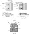
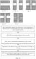
- FIG. 1 a diagram of a structure of a conventional vertical channel transistor and a corresponding band diagram (band diagram) are at a left side, and a diagram of a vertical channel transistor having a contact layer and a corresponding band diagram according to an embodiment of this application are at a right side.
- FIG. 1 in the conventional technology, electrons need to pass through two contact surfaces from a source to a semiconductor channel layer and then to a drain: a contact surface between the source and the semiconductor channel layer and a contact surface between the semiconductor channel layer and the drain.
- Both contact between the source and the semiconductor channel layer and contact between the semiconductor channel layer and the drain are Schottky contact, and a thermal excitation mode is used for current injection. As a result, a contact resistance is large, electronic potential energy required for passing through a barrier is large, and a current is small.
- a vertical channel transistor structure provided in this application is shown at the right side of FIG. 1 . Contact layers are respectively disposed between a drain and an insulation dielectric layer and between a source and the insulation dielectric layer.
- Electrons need to pass through four contact surfaces in total from the source to the drain: a contact surface between the source and a first contact layer, a contact surface between the first contact layer and a semiconductor channel layer, a contact surface between the semiconductor channel layer and a second contact layer, and a contact surface between the second contact layer and the drain.
- materials of the two contact layers are conductor materials or semiconductor materials whose conductivities are higher than that of the semiconductor channel layer, and resistances are low, performance of contact between the contact layer and the semiconductor channel layer is far better than performance of contact between the source and the semiconductor channel layer and contact between the drain and the semiconductor channel layer, a contact resistance of the contact surface between the contact layer and the semiconductor channel layer is far less than a contact resistance of the contact surface between the source and the semiconductor channel layer and a contact resistance of the contact surface between the drain and the semiconductor channel layer.
- the contact layer is in good contact with metal, in an ideal case, contact resistances formed between the source and the contact layer and between the drain and the contact layer may be ignored.
- a total resistance of the four contact surfaces through which the electrons pass from the source to the drain is less than a total resistance of the two contact surfaces through which the electrons pass from the source to the drain in the conventional technology, so that ohmic contact (which may also be referred to as ohmic-like contact) can be formed between the source and the semiconductor channel layer and between the drain and the semiconductor channel layer.
- ohmic contact which may also be referred to as ohmic-like contact
- the electrons may, through a barrier due to fluctuation, directly enter the semiconductor channel layer from the source and enter the drain from the semiconductor channel layer, that is, tunneling injection of a current is implemented.
- a contact resistance of the vertical channel transistor is greatly reduced, and a current flowing from the source to the drain is increased, that is, an operating current of the vertical channel transistor is increased.
- the contact resistance in this embodiment of this application may be understood as a sum of a resistance Rs between the source and the channel and a resistance Rd between the channel and the drain. It should be understood that the contact resistance and the sum of Rs and Rd may be only approximate, but not necessarily strictly equal.
- the contact resistance may also be referred to as a source-drain contact resistance.
- An embodiment of this application provides a vertical channel transistor structure.
- the structure includes a stacked structure.
- the stacked structure includes a first metal layer, a first contact layer, an insulation dielectric layer, a second contact layer, and a second metal layer.
- the first contact layer is located between the first metal layer and the insulation dielectric layer
- the second contact layer is located between the second metal layer and the insulation dielectric layer.
- a groove is disposed in the stacked structure.
- a semiconductor channel layer, a gate oxygen dielectric layer, and a gate are disposed in the groove.
- the semiconductor channel layer is separately in contact with the first metal layer and the second metal layer, and the gate oxygen dielectric layer is disposed between the semiconductor channel layer and the gate.
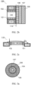
- FIG. 2a is a diagram of a structure of a vertical channel transistor according to an embodiment of this application
- FIG. 2b is a partially enlarged view of FIG. 2a
- FIG. 2c is a sectional view of FIG. 2b along a dashed line 110.
- the vertical channel transistor includes a drain (Drain) 103, a source (Source) 104, a gate (Gate) 105, a semiconductor channel layer 106, a gate oxygen dielectric layer 107, and an insulation dielectric layer 108, a first contact layer 101, and a second contact layer 102.
- the vertical channel transistor is of a columnar structure, and has a semiconductor channel in a vertical direction.
- the drain 103, the first contact layer 101, the insulation dielectric layer 108, the second contact layer 102, and the source 104 form a stacked structure in the vertical direction, where a deep hole or groove is disposed inside the stacked structure, the semiconductor channel layer 106, the gate oxygen dielectric layer 107, and the gate 105 are sequentially disposed in the deep hole, the semiconductor channel layer 106 forms contact with both the source 104 and the drain 103, and the gate oxygen dielectric layer 107 is disposed between the gate 105 and the semiconductor channel layer 106. It should be understood that locations of the source 104and the drain 103 may be interchanged. In FIG. 2a , the drain is at a lower side of the device, and the source is at an upper side of the device.
- the source is at a lower side of the device, and the drain is at an upper side of the device.
- the locations of the source and the drain are not limited in embodiments of this application.
- the vertical channel transistor in this embodiment of this application may be a vertical channel TFT.
- the deep hole in the stacked structure penetrates the source layer 104, the second contact layer 102, the insulation dielectric layer 108, and the first contact layer 101, and is recessed into the drain 103.
- the insulation dielectric layer 108 is disposed between the drain 103 and the source 104, so that electrical isolation between source metal and drain metal can be implemented.
- the first contact layer 101 is disposed between the drain 103 and the insulation dielectric layer 108
- the second contact layer 102 is disposed between the source 104 and the insulation dielectric layer 108.
- the two contact layers each have a low resistance and a high doping concentration, and are in good contact with metal, so that ohmic contact (which may also be referred to as ohmic-like contact) may be formed between the source 104 and the semiconductor channel layer 106, and between the drain 103 and the semiconductor channel layer 106.
- ohmic contact which may also be referred to as ohmic-like contact
- electrons may, through a barrier due to fluctuation, directly enter the semiconductor channel layer from the source and enter the drain from the semiconductor channel layer, that is, tunneling injection of a current is implemented.
- a contact resistance of the vertical channel transistor is greatly reduced, and a current flowing from the source to the drain is increased, that is, an operating current of the vertical channel transistor is increased.
- the insulation dielectric layer may also be referred to as a dielectric layer.
- a length of the vertical channel is determined based on a thickness d of the insulation dielectric layer. To some extent, the length of the vertical channel is approximately equal to the thickness d of the insulation dielectric layer.
- first contact layer 101 and the second contact layer 102 each may also be referred to as a transition layer, an ohmic contact layer, or an ohmic contact intercalation layer.
- Names of the contact layers are not limited in embodiments of this application.
- materials of the first contact layer and the second contact layer are conductor materials or semiconductor materials whose conductivities are higher than that of the semiconductor channel layer. If the materials of the first contact layer and the second contact layer are the conductor materials, the conductor materials of the first contact layer and the second contact layer are different from materials of the first metal layer and the second metal layer. The materials of the first contact layer and the second contact layer can form good contact with the semiconductor channel layer.
- a contact resistance of a contact surface between the contact layer and the semiconductor channel layer is far less than a contact resistance of a contact surface between the source and the semiconductor channel layer and a contact resistance of a contact surface between the drain and the semiconductor channel layer.
- a resistance of a contact surface formed between the first contact layer and the first metal layer and a resistance of a contact surface formed between the second contact layer and the second metal layer are less than a first threshold.
- the first threshold is close to 0. Therefore, the resistance of the contact surface formed between the contact layer and the metal layer may be ignored.
- a sum of the resistance of the contact surface formed between the first contact layer and the first metal layer and a resistance of a contact surface formed between the first contact layer and the semiconductor channel layer is less than a resistance of a contact surface formed between the first metal layer and the semiconductor channel layer.
- a sum of the resistance of the contact surface formed between the second contact layer and the second metal layer and a resistance of a contact surface formed between the second contact layer and the semiconductor channel layer is less than a resistance of a contact surface formed between the second metal layer and the semiconductor channel layer.
- the materials of the first contact layer and the second contact layer are related to a material of the semiconductor channel layer.
- the materials of the first contact layer and the second contact layer are the conductor materials
- the semiconductor channel layer is an N-type semiconductor
- the materials of the first contact layer and the second contact layer are first conductor materials, where a work function of the first conductor material is less than or close to electron affinity of the semiconductor channel layer; or if the semiconductor channel layer is a P-type semiconductor, the materials of the first contact layer and the second contact layer are second conductor materials, where a work function of the second conductor material is greater than or close to a sum of electron affinity and a band gap of the semiconductor channel layer.
- the materials of the first contact layer and the second contact layer are the semiconductor materials
- the semiconductor channel layer is a first N-type semiconductor
- the materials of the first contact layer and the second contact layer are first semiconductor materials, where a conduction band location of the first semiconductor material is close to a conduction band location of the first N-type semiconductor, and a conductivity of the first semiconductor material is greater than or equal to a conductivity of the first N-type semiconductor
- the semiconductor channel layer is a first P-type semiconductor
- the materials of the first contact layer and the second contact layer are second semiconductor materials, where a valence band location of the second conductor material is close to a valence band location of the first P-type semiconductor, and a conductivity of the second conductor material is greater than or equal to a conductivity of the first P-type semiconductor.
- Work function is minimum energy that needs to be provided to enable an electron to escape from a surface of a solid immediately. Generally, a unit is electron volt. Here, the term “immediately” indicates that a final electron location is far away from the surface at an atomic scale but still close to the solid at a macroscopic scale.
- the work function is an important attribute of metal.
- Electron affinity (electron affinity): The electron affinity may also be referred to as electron affinity potential or electron affinity and is energy of the affinity between electrons.
- the electron affinity is energy released when a gaseous atom in a ground state obtains an electron to become a gaseous anion. A unit is kJ/mol.
- the electron affinity indicates energy consumed or released to separate an electron from a gaseous ion or molecule.
- Conduction band (conduction band): The conduction band is an energy space formed by a free electron, namely, an energy range of the electron moving freely in a solid structure.
- Valence band (valence band): The valence band is a highest-energy region in which an electron in a solid at absolute zero is located. If an electron in the valence band is given energy higher than a band gap, the electron transits from the valence band to a conduction band. In short, a band occupied by valence electrons is the valence band.
- Forbidden band (forbidden band):
- the forbidden band usually indicates an energy range whose density of states is zero between a valence band and a conduction band.
- a gap between the conduction band and the valence band is the forbidden band.
- Band gap (band gap or width of forbidden band):
- the band gap indicates an energy range of a forbidden band. To become a free electron or a hole, a bound electron needs to obtain enough energy to transit from a valence band to a conduction band. A minimum value of this energy is the band gap. In other words, the band gap is energy between a lowest energy level of the conduction band and a highest energy level of the valence band.
- a contact layer may use a same semiconductor as a semiconductor channel, but the semiconductor at the contact layer needs to be doped or processed in another way, so that the contact layer has a lower resistance than the semiconductor channel layer.
- the first contact layer and the second contact layer are semiconductors, the first contact layer and the second contact layer may also be referred to as doped semiconductor layers.
- an ohmic contact layer is introduced, so that in a condition that an area of a transistor device is not increased, a contact area between a channel and a source/drain can be increased, to effectively reduce a contact resistance, and a threshold of a channel material is kept unchanged, to improve device performance.
- a first contact layer 101 and a second contact layer 102 each may select a highly conductive oxide semiconductor, for example, indium gallium zinc oxide InGaZnO, indium zinc oxide InZnO, indium tin oxide InSnO, indium oxide In2O3, gallium oxide Ga2O3, indium titanium oxide InTiO, and zinc oxide ZnO, may select a conductor, for example, titanium Ti, gold Au, tungsten W, molybdenum Mo, aluminum Al, and titanium nitride TiN, or may select heavily doped P-type silicon Si and N-type Si, or any combination of the P-type silicon Si and the N-type Si.
- a highly conductive oxide semiconductor for example, indium gallium zinc oxide InGaZnO, indium zinc oxide InZnO, indium tin oxide InSnO, indium oxide In2O3, gallium oxide Ga2O3, indium titanium oxide InTiO, and zinc oxide ZnO
- a conductor for example, titanium Ti, gold Au
- a source 104 and a drain 103 may use a metal material or a conductive material, for example, TiN, Ti, Au, W, Mo, In-Ti-O (ITO), Al, copper Cu, ruthenium Ru, silver Ag, or any combination thereof.
- a metal material or a conductive material for example, TiN, Ti, Au, W, Mo, In-Ti-O (ITO), Al, copper Cu, ruthenium Ru, silver Ag, or any combination thereof.
- a gate 105 may be made of a metal material or a conductive material, for example, TiN, Ti, Au, W, Mo, InTiO, InZnO, Al, Cu, Ru, Ag, or any combination thereof.
- a material of a gate oxygen dielectric layer 107 may be an insulation material such as SiO2, Al2O3, HfO2, ZrO2, TiO2, Y2O3, LaOx, or Si3N4, or any combination material thereof.
- the gate oxygen dielectric layer 107 may be of a stacked structure of a single material or a stacked structure of a combination material.
- the material of the semiconductor channel layer 106 may be Si, polysilicon poly-Si, amorphous silicon amorphous-Si, a multi-composite compound such as IGZO, a semiconductor material such as In2O3, Ga2O3, ZnO, SnOx, ITO, TiO2, and MoS2, or any combination thereof.
- a material of the insulation dielectric layer 108 may be a material such as SiO2, Si3N4, or Al2O3.
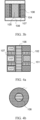
- FIG. 3a is a top view of an example of a vertical channel transistor according to an embodiment of this application.
- the vertical channel transistor is cylindrical.
- An innermost layer of the cylinder is a gate 105, the gate 105 is wrapped with a gate oxygen dielectric layer 107, the gate oxygen dielectric layer is wrapped with a semiconductor channel layer 106, and an outer layer of the semiconductor channel layer 106 is wrapped with a stacked structure formed by a source layer, a drain layer, and the like.
- FIG. 3a is the top view, only the source layer 104 at a top layer can be seen.
- This implementation is a channel-all-around (Channel-All-Around, CAA) manner.
- the semiconductor channel layer 106 is completely filled in a vertical groove inside the stacked structure.
- FIG. 3b is a top view of another example of a vertical channel transistor according to an embodiment of this application.
- the vertical channel transistor is of a double-channel structure, and the vertical channel transistor is of a square columnar structure. Therefore, the top view of the vertical channel transistor is rectangular, an entire stacked structure formed by a drain 103, a first contact layer 101, an insulation dielectric layer 108, a second contact layer 102, and a source 104 in a vertical direction is the square columnar structure, or may be referred to as a cube.
- the drain 103, the first contact layer 101, the insulation dielectric layer 108, and the second contact layer 102 are all located below the source 104, only the topmost source 104 can be seen in the top view 3b.
- two side walls remain, and a semiconductor channel layer 106, a gate oxygen dielectric layer 107, and a gate 105 are sequentially disposed on an inner side of each of the two side walls.
- the two semiconductor channel layers 106 are disposed close to the two side walls of the transistor, thereby generating two perpendicular channels.
- the two side walls are respectively referred to as a first stacked substructure and a second stacked substructure, and a gate is disposed between the first stacked substructure and the second stacked substructure.
- a first semiconductor channel layer and a first gate oxygen dielectric layer are disposed between the first stacked substructure and the gate, and the first semiconductor channel layer is in contact with a side surface of the first stacked substructure.
- a second semiconductor channel layer and a second gate oxygen dielectric layer are disposed between the second stacked substructure and the gate, and the second semiconductor channel layer is in contact with a side surface of the second stacked substructure.
- the first semiconductor channel layer is in contact with the side surface of the first stacked substructure to form one vertical channel
- the second semiconductor channel layer is in contact with the side surface of the second stacked substructure to form the other vertical channel. Therefore, the vertical channel transistor has two vertical channels.
- the double-channel structure can further increase an operating current of the vertical channel transistor device, and further increase an operating speed of a memory in which the vertical channel transistor is located.
- FIG. 3b the two insulation dielectric layers 108 shown in FIG. 3b are configured to isolate adjacent vertical channel transistors, and are not a part of the vertical channel transistors.
- the insulation dielectric layers in FIG. 3a and FIG. 3b each may have a side view shown in FIG. 2a .
- FIG. 3a and FIG. 3b may be two possible top views corresponding to the side view of the vertical channel transistor shown in FIG. 2a .
- a square deep hole may also be disposed inside the square columnar structure, and the semiconductor channel layer 106, the gate oxygen dielectric layer 107, and the gate 105 are sequentially disposed in the square deep hole.
- the semiconductor channel layer 106 is located inside the square column, the semiconductor channel layer 106 completely wraps the gate oxygen dielectric layer 107, and the gate oxygen dielectric layer also completely wraps the gate 105.
- a cross-sectional view of the vertical channel transistor in a top view direction may also be another shape except for a circle and a square, for example, may be a polygon, a sector, or an irregular shape.
- an embodiment of this application further provides a vertical channel transistor, including a stacked structure and a semiconductor channel layer, where the stacked structure is provided with a vertical groove, and the semiconductor channel layer is disposed in the groove.
- the stacked structure includes a first metal layer, a second metal layer, and a third metal layer, the third metal layer is located between the first metal layer and the second metal layer, a first interface, a second interface, and a third interface of the third metal layer are wrapped with a first dielectric layer, the first interface is an interface that is of the third metal layer and that faces the first metal layer, the second interface is an interface that is of the third metal layer and that faces the second metal layer, and the third interface is an interface that is of the third metal layer and that faces the semiconductor channel layer.
- the stacked structure further includes a first contact layer and a second contact layer, the first contact layer is located between the first metal layer and the first dielectric layer, and the second contact layer is located between the second metal layer and the first dielectric layer.
- the semiconductor channel layer is separately in contact with the first metal layer and the second metal layer. It should be understood that one of the first metal layer and the second metal layer is a source, the other is a drain, and the third metal layer is a gate.
- the first dielectric layer may also be referred to as a gate oxygen dielectric layer. It should be understood that for the first contact layer and the second contact layer in this embodiment of this application, refer to the foregoing descriptions. Details are not described herein again.
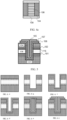
- FIG. 4a is a side cross-sectional view of another vertical channel transistor according to an embodiment of this application.
- FIG. 4b is a top view corresponding to the vertical channel transistor in FIG. 4a .
- FIG. 4c is another top view corresponding to the vertical channel transistor in FIG. 4a .
- a vertical channel layer 106 is fully filled in a vertical channel in a stacked structure, and the channel penetrates the entire stacked structure.
- a source 104 and a drain 103 are located at the top and the bottom of the device respectively.
- a gate 105 is located between the source 104 and the drain 103 in a vertical direction. The gate 105 regulates a current in the semiconductor channel layer 106 from an outer side.
- a gate oxygen dielectric layer 107 is disposed on a surface that is of the gate 105 and that faces the source 104, a surface that is of the gate and that faces the drain 103, and a surface that is of the gate and that is close to the semiconductor channel layer.
- a first contact layer 101 is located between the drain 103 and the gate oxygen dielectric layer 107, and a second contact layer 102 is located between the source 104 and the gate oxygen dielectric layer 107, so that the source and the drain separately form ohmic contact with the vertical channel layer 106.
- the structure effectively reduces a contact resistance and improves device performance.
- the gate and the gate oxygen dielectric layer are disposed between the source 104 and the drain 103, and an insulation dielectric layer 108 is omitted. Therefore, a size of the transistor device may be smaller, to facilitate improvement of integration.
- the vertical channel transistor shown in FIG. 4a may be made into a cylindrical structure.
- This implementation is a GAA manner, and the vertical channel layer 106 is completely filled in the vertical channel in the stacked structure, and is wrapped with the source 104, the drain 103, and the gate 105 that are surrounded in a horizontal direction.
- the vertical channel transistor shown in FIG. 4a may be made into a square columnar structure, and the entire stacked structure formed by the drain 103, the first contact layer 101, the gate 105, the gate oxygen dielectric layer 107, the second contact layer 102, and the source 104 in the vertical direction is the square columnar structure, or may be referred to as a cube structure. It should be explained that, because the drain 103, the first contact layer 101, the gate 105, the gate oxygen dielectric layer 107, and the second contact layer 102 are all located below the source 104, only the topmost source 104 can be seen in the top view 4c. Two side walls remain after a middle part of the stacked structure is etched.
- the semiconductor channel layer 106 is disposed between the two side walls.
- the source 104 and the drain 103 are located at the top and the bottom of the vertical channel transistor device respectively.
- the gate 105 is located between the source 104 and the drain 103, and the semiconductor channel layer 106 extends in the vertical direction. Therefore, the structure shown in FIG. 4c is a double-gate structure, and a vertical channel is generated on each of two surfaces that are of the semiconductor channel layer 106 and that are in contact with the stacked structure.
- two insulation dielectric layers 108 shown in FIG. 4c are configured to isolate adjacent vertical channel transistors, and are not a part inside the vertical channel transistors.
- cylindrical structure shown in FIG. 4b may also be made into a square columnar structure, and a cross-sectional view of the vertical channel transistor shown in FIG. 4a in a top view direction may also be another shape except for a circle and a square, for example, may be a polygon, a sector, or an irregular shape.
- the ohmic contact may be formed between the source/drain and the semiconductor channel layer after the ohmic contact layer is introduced. If a material of an ohmic contact layer and a material of the semiconductor channel layer have inconsistent polarities, doping concentration of the ohmic contact layer needs to be increased, to form PN junction ohmic contact between the source/drain and the semiconductor channel layer.
- Materials of the first contact layer 101 and the second contact layer 102 may be selected based on the material of the semiconductor channel layer, to implement the PN junction ohmic contact. If the semiconductor channel material is an N-type semiconductor, the first contact layer 101 and the second contact layer 102 may use a P-type semiconductor to form PN junction contact. If the semiconductor channel material is a P-type semiconductor, the first contact layer 101 and the second contact layer 102 may use an N-type semiconductor to form PN junction contact. Further, a contact resistance of a PN junction is reduced by increasing doping concentration of the first contact layer 101 and the second contact layer 102, to form the PN junction ohmic contact between the source/drain and the semiconductor channel layer. This expands selection of a device material, this solution can be widely used to optimize a contact resistance of a device made of any material, and this implements a heterogeneous-contact transistor device.
- FIG. 5 is a diagram of a structure of another vertical channel transistor according to an embodiment of this application.
- interface layers 116 are respectively added between a first contact layer 101 and an insulation dielectric layer 108, and between a second contact layer 102 and the insulation dielectric layer 108.
- the interface layer 116 may use a material that is the same as materials of the first contact layer 101 and the second contact layer 102.
- doping concentration of the material of the interface layer 116 is different from that of the materials of the first contact layer 101 and the second contact layer 102, doping concentration of the first contact layer 101 and the second contact layer 102 is high, and doping concentration of the interface layer 116 is low.
- the interface layers 116 can effectively prevent heavily doped elements from diffusing into the insulation dielectric layer 108, thereby expanding doping concentration windows of the contact layer 101 and the contact layer 102.
- the contact layer 101 and the contact layer 102 may be doped at higher concentration, so that resistances of formed PN junction ohmic contact are smaller.
- the heavily doped element can be prevented from diffusing into the insulation isolation layer 108, and isolation effect of the insulation isolation layer 108 is not affected.
- the interface layer 116 may also be introduced into the vertical channel transistor shown in FIG. 4a .
- the interface layers may be respectively introduced at an interface between the first contact layer 101 and the gate oxygen dielectric layer 107 and an interface between the second contact layer 102 and the gate oxygen dielectric layer 107, to effectively prevent the heavily doped element from diffusing into the gate oxygen dielectric layer 107.
- FIG. 6a to FIG. 6f are a schematic flowchart of a manufacturing process of a vertical channel transistor according to an embodiment of this application.
- FIG. 7 is a schematic flowchart of a method for manufacturing a vertical channel transistor according to an embodiment of this application.
- the method includes the following steps.
- the base may also be referred to as a substrate, and a material of the base may be an insulation material such as silicon oxide.
- a material of the base may be an insulation material such as silicon oxide.
- locations of a source and a drain may be interchanged. If a drain layer is located at a lower part, a source layer is located at an upper part. On the contrary, if a source layer is located at a lower part, a drain layer is located at an upper part.
- the first contact layer and the second contact layer may be low-resistance semiconductors. For materials of the five layers, refer to the foregoing descriptions of the materials of the source 104, the drain 103, the insulation dielectric layer 108, the first contact layer 101, and the second contact layer 102. Details are not described herein again.
- a first interface layer may be further grown between the first contact layer and the insulation dielectric layer, and a second interface layer may be grown between the second contact layer and the insulation dielectric layer.
- first interface layer and the second interface layer refer to the foregoing description of the interface layer 116. Details are not described herein again.
- a groove shown in FIG. 6b may be referred to as a first groove.
- etching is one-step etching.
- the etching process may use dry etching or wet etching.
- a groove in FIG. 6c may be referred to as a second groove.
- a semiconductor channel layer may be grown by using an atomic layer deposition (Atomic Layer Deposition, ALD) process or a chemical vapor deposition (Chemical Vapor Deposition, CVD) process.
- ALD atomic layer deposition
- CVD chemical vapor deposition
- the semiconductor channel material refer to the foregoing description of the semiconductor channel material 106. Details are not described herein again.
- a gate oxygen dielectric material based on the structure shown in FIG. 6c to form a structure shown in FIG. 6d .
- a groove in FIG. 6d may be referred to as a third groove.
- the gate oxygen dielectric layer may also be grown by using the ALD process or the CVD process.
- the gate oxygen dielectric material refer to the foregoing description of the material of the gate oxygen dielectric layer 107. Details are not described herein again.
- the gate metal is filled in the third groove in FIG. 6d to form a gate.
- a gate layer may also be grown by using the ALD process or the CVD process.
- 701 specifically includes: sequentially growing the metal layer, the first contact layer, the first interface layer, the insulation dielectric layer, the second interface layer, the second contact layer, and the metal layer on the base to obtain a seven-layer structure, to manufacture the vertical channel transistor shown in FIG. 5 .
- FIG. 8 is a schematic flowchart of another method for manufacturing a vertical channel transistor according to an embodiment of this application.
- the groove penetrates the upper metal layer, the low-resistance semiconductor layer, the insulation dielectric layer, and the low-resistance semiconductor layer, and is recessed into the lower metal layer.
- the semiconductor channel layer, the gate oxygen dielectric layer, and the gate layer may be all grown by using an ALD process or a CVD process.
- 801 specifically includes: sequentially depositing the metal layer, the first contact layer, the first interface layer, the insulation dielectric layer, the second interface layer, the second contact layer, and the metal layer to obtain a stacked structure including seven layers, to manufacture the vertical channel transistor shown in FIG. 5 .
- a conventional process is applied to the vertical channel transistor.
- the source and the drain need to be doped, and then when the structure shown in FIG. 6c is formed, the semiconductor channel layer is doped, to reduce a contact resistance between the source/drain and the semiconductor channel. Because the semiconductor channel layer is perpendicular, doping concentration is uneven in an upper part and a lower part of the semiconductor channel layer when the semiconductor channel layer is bombarded through an ion beam to implement doping, and doping concentration is also uneven in an upper part and a lower part when the source and the drain are doped.
- an ohmic contact layer is introduced to reduce the contact resistance between the source/drain and the semiconductor channel layer, and the contact resistance does not need to be reduced by doping the source, the drain, and the semiconductor channel layer. Therefore, a problem of uneven doping concentration is avoided, and an additional photomask required for a doping process does not need to be added.
- the process is simple, and application costs are reduced.
- source/drain metal is in contact with the semiconductor channel, a contact surface is oxidized to some extent in an annealing process, and oxidation increases the contact resistance. After the contact layer is introduced, even if the metal is oxidized, the contact resistance of the transistor device is not greatly affected. Therefore, negative effect of a contact resistance increase due to oxidation of the contact surface between the metal and the channel caused by subsequent annealing can be avoided, and thermal stability of the device can be improved.
- the interface layer can effectively prevent a heavily doped element from diffusing into the insulation dielectric layer, thereby expanding a doping concentration window of the contact layer.
- the contact layer can be doped at higher concentration, so that a resistance of formed PN junction ohmic contact is smaller.
- the heavily doped element can be prevented from diffusing into the insulation isolation layer, and isolation effect of the insulation isolation layer is not affected.
- FIG. 9a to FIG. 9e are a schematic flowchart of a manufacturing process of a vertical channel transistor according to an embodiment of this application.
- FIG. 10 is a schematic flowchart of a corresponding method for manufacturing a vertical channel transistor according to an embodiment of this application. The manufacturing process shown in FIG. 9a to FIG. 9e and FIG. 10 may be used to manufacture the vertical channel transistor shown in FIG. 4a .
- the method includes the following steps.
- 1001 Sequentially deposit a first metal layer, a first contact layer, a dielectric layer, a second contact layer, and a second metal layer to form a stacked structure, as shown in FIG. 9a .
- first metal layer and the second metal layer is a source, and the other is a drain.
- the first contact layer and the second contact layer may be low-resistance semiconductor layers.
- optional materials of the five layers respectively refer to the foregoing descriptions of the materials of the drain 103, the first contact layer 101, the insulation dielectric layer 108, the second contact layer 102, and the source 104. Details are not described herein again.
- a first interface layer may be further grown between the first contact layer and the insulation dielectric layer, and a second interface layer may be grown between the second contact layer and the insulation dielectric layer.
- first interface layer and the second interface layer refer to the foregoing description of the interface layer 116. Details are not described herein again.
- the via hole may also be referred to as a groove that penetrates the stacked structure in a vertical direction.
- Etching is one-step etching.
- 1003 Grow a semiconductor channel layer in the via hole to form a structure shown in FIG. 9c .
- the semiconductor channel layer may be grown by using an ALD process or a CVD process.
- the semiconductor channel material refer to the foregoing description of the semiconductor channel material 106. Details are not described herein again.
- two spaces are formed, and are located on two sides of the semiconductor channel layer.
- the gate oxygen dielectric layers are first grown through ALD or CVD, and then the gates are respectively grown on the gate oxygen dielectric layers through ALD or the CVD.
- the groove formed after the dielectric layer is removed has three surfaces: a first side surface facing the first contact layer, an adjacent second side surface facing the second contact layer, and a third surface in contact with the semiconductor channel layer.
- a gate oxygen dielectric layer is grown on all of the three surfaces.
- For the gate oxygen dielectric material refer to the foregoing description of the material of the gate oxygen dielectric layer 107. Details are not described herein again.
- the method may further include the following step.
- the interface layers may be respectively formed between the first contact layer and the dielectric layer, and between the second contact layer and the dielectric layer, that is, the metal layer, the first contact layer, the first interface layer, the dielectric layer, the second interface layer, the second contact layer, and the metal layer are sequentially deposited, to obtain a stacked structure including seven layers, to manufacture the vertical channel transistor including the interface layers. Then, subsequent processing of steps 1002 to 1005 is performed on the stacked structure.
- an ohmic contact layer is introduced to reduce a contact resistance between the source/drain and the semiconductor channel layer, and the contact resistance does not need to be reduced by doping the source, the drain, and the semiconductor channel layer. Therefore, a problem of uneven doping concentration is avoided, and an additional photomask required for a doping process does not need to be added.
- the process is simple, and application costs are reduced.
- source/drain metal is in contact with the semiconductor channel, a contact surface is oxidized to some extent in an annealing process, and oxidation increases the contact resistance. After the contact layer is introduced, even if the metal is oxidized, a contact resistance of the transistor device is not greatly affected. Therefore, negative effect of a contact resistance increase due to oxidation of the contact surface between the metal and the channel caused by subsequent annealing can be avoided, and thermal stability of the device can be improved.
Landscapes
- Thin Film Transistor (AREA)
- Electrodes Of Semiconductors (AREA)
Applications Claiming Priority (2)
| Application Number | Priority Date | Filing Date | Title |
|---|---|---|---|
| CN202210247054.2A CN116799057B (zh) | 2022-03-14 | 2022-03-14 | 一种垂直沟道晶体管结构及制造方法 |
| PCT/CN2023/071143 WO2023173914A1 (zh) | 2022-03-14 | 2023-01-08 | 一种垂直沟道晶体管结构及其制造方法 |
Publications (2)
| Publication Number | Publication Date |
|---|---|
| EP4478423A1 true EP4478423A1 (de) | 2024-12-18 |
| EP4478423A4 EP4478423A4 (de) | 2025-10-22 |
Family
ID=88022169
Family Applications (1)
| Application Number | Title | Priority Date | Filing Date |
|---|---|---|---|
| EP23769425.2A Pending EP4478423A4 (de) | 2022-03-14 | 2023-01-08 | Transistorstruktur mit vertikalem kanal und herstellungsverfahren dafür |
Country Status (4)
| Country | Link |
|---|---|
| US (1) | US20250008746A1 (de) |
| EP (1) | EP4478423A4 (de) |
| CN (1) | CN116799057B (de) |
| WO (1) | WO2023173914A1 (de) |
Families Citing this family (5)
| Publication number | Priority date | Publication date | Assignee | Title |
|---|---|---|---|---|
| US12457768B2 (en) * | 2022-05-20 | 2025-10-28 | Tokyo Electron Limited | Vertical transistors and methods for forming the same |
| US12342681B2 (en) * | 2023-09-15 | 2025-06-24 | Industrial Technology Research Institute | All-oxide transistor structure, method for fabricating the same and display panel comprising the structure |
| CN120434989A (zh) * | 2024-02-04 | 2025-08-05 | 华为技术有限公司 | 芯片及其制备方法、存储器、电子设备 |
| CN121057258A (zh) * | 2024-05-23 | 2025-12-02 | 华为技术有限公司 | 半导体结构及其制备方法、存储阵列、存储器、逻辑器件、电子设备 |
| CN119486169B (zh) * | 2024-10-16 | 2025-10-14 | 长鑫科技集团股份有限公司 | 半导体结构及其制备方法 |
Family Cites Families (16)
| Publication number | Priority date | Publication date | Assignee | Title |
|---|---|---|---|---|
| US7629633B2 (en) * | 2004-05-20 | 2009-12-08 | Isaac Wing Tak Chan | Vertical thin film transistor with short-channel effect suppression |
| KR100852628B1 (ko) * | 2007-02-05 | 2008-08-18 | 연세대학교 산학협력단 | 1d 나노와이어 채널을 이용한 박막트랜지스터의 제조방법 |
| TWI328788B (en) * | 2008-03-11 | 2010-08-11 | Au Optronics Corp | Gate driver-on-array and method of making the same |
| JP2010040897A (ja) * | 2008-08-07 | 2010-02-18 | Sony Corp | 有機薄膜トランジスタ、有機薄膜トランジスタの製造方法、および電子機器 |
| CN101404321B (zh) * | 2008-10-31 | 2011-04-20 | 中国科学院微电子研究所 | 一种垂直沟道有机场效应晶体管的制备方法 |
| JP5488136B2 (ja) * | 2010-04-05 | 2014-05-14 | セイコーエプソン株式会社 | 電気光学装置及び電子機器並びにトランジスター |
| CN102263200A (zh) * | 2010-05-25 | 2011-11-30 | 中国科学院微电子研究所 | 一种有机场效应晶体管及其制备方法 |
| KR101916222B1 (ko) * | 2011-04-29 | 2018-11-08 | 삼성전자 주식회사 | 수직 구조의 비휘발성 메모리 소자 및 그 제조 방법 |
| US9508860B2 (en) * | 2014-12-31 | 2016-11-29 | Shenzhen China Star Optoelectronics Technology Co., Ltd. | Lateral gate electrode TFT switch and liquid crystal display device |
| WO2016128859A1 (en) * | 2015-02-11 | 2016-08-18 | Semiconductor Energy Laboratory Co., Ltd. | Semiconductor device and manufacturing method thereof |
| US9583615B2 (en) * | 2015-02-17 | 2017-02-28 | Sandisk Technologies Llc | Vertical transistor and local interconnect structure |
| WO2018063165A1 (en) * | 2016-09-27 | 2018-04-05 | Intel Corporation | Non-planar gate thin film transistor |
| US9806191B1 (en) * | 2016-10-11 | 2017-10-31 | United Microelectronics Corp. | Vertical channel oxide semiconductor field effect transistor and method for fabricating the same |
| JP7109928B2 (ja) * | 2018-01-31 | 2022-08-01 | キオクシア株式会社 | トランジスタ及び半導体記憶装置並びにトランジスタの製造方法 |
| EP3882978A1 (de) * | 2020-03-16 | 2021-09-22 | Samsung Electronics Co., Ltd. | Vertikaler transistor, inverter damit und vertikale halbleiteranordnung damit |
| CN114122145B (zh) * | 2021-11-15 | 2023-11-28 | 武汉华星光电半导体显示技术有限公司 | 薄膜晶体管、电子装置及其制备方法及显示装置 |
-
2022
- 2022-03-14 CN CN202210247054.2A patent/CN116799057B/zh active Active
-
2023
- 2023-01-08 WO PCT/CN2023/071143 patent/WO2023173914A1/zh not_active Ceased
- 2023-01-08 EP EP23769425.2A patent/EP4478423A4/de active Pending
-
2024
- 2024-09-13 US US18/885,345 patent/US20250008746A1/en active Pending
Also Published As
| Publication number | Publication date |
|---|---|
| EP4478423A4 (de) | 2025-10-22 |
| CN116799057A (zh) | 2023-09-22 |
| WO2023173914A1 (zh) | 2023-09-21 |
| CN116799057B (zh) | 2025-12-16 |
| US20250008746A1 (en) | 2025-01-02 |
Similar Documents
| Publication | Publication Date | Title |
|---|---|---|
| EP4478423A1 (de) | Transistorstruktur mit vertikalem kanal und herstellungsverfahren dafür | |
| KR102831126B1 (ko) | 이차원 물질로 이루어진 게이트 절연막을 포함하는 전계 효과 트랜지스터 | |
| US9190491B1 (en) | Variable resistive memory device including vertical channel PMOS transistor and method of manufacturing the same | |
| US12029029B2 (en) | Semiconductor memory devices | |
| US9166004B2 (en) | Semiconductor device contacts | |
| US9373620B2 (en) | Series connected transistor structure and method of manufacturing the same | |
| US11127825B2 (en) | Middle-of-line contacts with varying contact area providing reduced contact resistance | |
| US10529817B2 (en) | Semiconductor devices having multi-threshold voltage | |
| US11430889B2 (en) | Junctionless field-effect transistor having metal-interlayer-semiconductor structure and manufacturing method thereof | |
| US12317514B2 (en) | Resistive random-access memory structures with stacked transistors | |
| JP5305739B2 (ja) | キャパシタレスメモリ | |
| US20250287605A1 (en) | Semiconductor device with low current leakage and method for manufacturing the same | |
| JP2010093051A (ja) | 電界効果型半導体装置 | |
| US20240206159A1 (en) | Integrated circuit devices and methods of forming the same | |
| US20230118661A1 (en) | Space-free vertical field effect transistor including active layer having vertically grown crystal grains | |
| US20240379657A1 (en) | Stacked devices containing at least one lateral diode | |
| US20250374621A1 (en) | Semiconductor device and method for fabricating the same | |
| US20260025977A1 (en) | Semiconductor devices having active patterns | |
| KR102654151B1 (ko) | 트랜지스터 및 이의 제조방법 | |
| US12526979B2 (en) | Memory and method for manufacturing memory | |
| US12402321B2 (en) | Vertical channel semiconductor device with ferroelectric-insulator gate stack | |
| JP7724363B2 (ja) | 3次元ダイナミックランダムアクセスメモリのための半導体分離ブリッジ | |
| US20250220887A1 (en) | Semiconductor device and method for fabricating the same | |
| US20250126768A1 (en) | Late sram cut with backside contact | |
| US20260075833A1 (en) | Ferroelectric field effect transistor having vertical structure, semiconductor device including ferroelectric field effect transistor, and operating method of semiconductor device |
Legal Events
| Date | Code | Title | Description |
|---|---|---|---|
| STAA | Information on the status of an ep patent application or granted ep patent |
Free format text: STATUS: THE INTERNATIONAL PUBLICATION HAS BEEN MADE |
|
| PUAI | Public reference made under article 153(3) epc to a published international application that has entered the european phase |
Free format text: ORIGINAL CODE: 0009012 |
|
| STAA | Information on the status of an ep patent application or granted ep patent |
Free format text: STATUS: REQUEST FOR EXAMINATION WAS MADE |
|
| 17P | Request for examination filed |
Effective date: 20240910 |
|
| AK | Designated contracting states |
Kind code of ref document: A1 Designated state(s): AL AT BE BG CH CY CZ DE DK EE ES FI FR GB GR HR HU IE IS IT LI LT LU LV MC ME MK MT NL NO PL PT RO RS SE SI SK SM TR |
|
| DAV | Request for validation of the european patent (deleted) | ||
| DAX | Request for extension of the european patent (deleted) | ||
| REG | Reference to a national code |
Ref country code: DE Ref legal event code: R079 Free format text: PREVIOUS MAIN CLASS: H01L0029780000 Ipc: H10D0030010000 |
|
| A4 | Supplementary search report drawn up and despatched |
Effective date: 20250922 |
|
| RIC1 | Information provided on ipc code assigned before grant |
Ipc: H10D 30/01 20250101AFI20250916BHEP Ipc: H10D 30/67 20250101ALI20250916BHEP Ipc: H10D 64/62 20250101ALI20250916BHEP Ipc: H10D 30/47 20250101ALN20250916BHEP Ipc: H10D 62/80 20250101ALN20250916BHEP |