EP4474366A1 - Verbundmaterial - Google Patents
Verbundmaterial Download PDFInfo
- Publication number
- EP4474366A1 EP4474366A1 EP24154022.8A EP24154022A EP4474366A1 EP 4474366 A1 EP4474366 A1 EP 4474366A1 EP 24154022 A EP24154022 A EP 24154022A EP 4474366 A1 EP4474366 A1 EP 4474366A1
- Authority
- EP
- European Patent Office
- Prior art keywords
- region
- composite material
- peak
- cross
- section
- Prior art date
- Legal status (The legal status is an assumption and is not a legal conclusion. Google has not performed a legal analysis and makes no representation as to the accuracy of the status listed.)
- Pending
Links
- 239000002131 composite material Substances 0.000 title claims abstract description 108
- HBMJWWWQQXIZIP-UHFFFAOYSA-N silicon carbide Chemical compound [Si+]#[C-] HBMJWWWQQXIZIP-UHFFFAOYSA-N 0.000 claims abstract description 52
- 229910010271 silicon carbide Inorganic materials 0.000 claims abstract description 49
- 229910052710 silicon Inorganic materials 0.000 claims abstract description 40
- 239000010703 silicon Substances 0.000 claims abstract description 40
- 238000012545 processing Methods 0.000 description 41
- XUIMIQQOPSSXEZ-UHFFFAOYSA-N Silicon Chemical compound [Si] XUIMIQQOPSSXEZ-UHFFFAOYSA-N 0.000 description 33
- 230000000052 comparative effect Effects 0.000 description 31
- 238000009826 distribution Methods 0.000 description 22
- 239000000843 powder Substances 0.000 description 21
- 238000010586 diagram Methods 0.000 description 12
- 239000002245 particle Substances 0.000 description 11
- 238000004519 manufacturing process Methods 0.000 description 10
- OKTJSMMVPCPJKN-UHFFFAOYSA-N Carbon Chemical compound [C] OKTJSMMVPCPJKN-UHFFFAOYSA-N 0.000 description 9
- 238000005259 measurement Methods 0.000 description 9
- 238000000465 moulding Methods 0.000 description 9
- 239000000463 material Substances 0.000 description 8
- 238000007790 scraping Methods 0.000 description 7
- 238000000034 method Methods 0.000 description 6
- 229910052799 carbon Inorganic materials 0.000 description 5
- 239000002994 raw material Substances 0.000 description 5
- 239000002002 slurry Substances 0.000 description 5
- 238000005488 sandblasting Methods 0.000 description 4
- 239000004065 semiconductor Substances 0.000 description 4
- 239000011230 binding agent Substances 0.000 description 3
- 238000004364 calculation method Methods 0.000 description 3
- 238000005520 cutting process Methods 0.000 description 3
- 239000002270 dispersing agent Substances 0.000 description 3
- 238000002474 experimental method Methods 0.000 description 3
- 238000005245 sintering Methods 0.000 description 3
- 238000009694 cold isostatic pressing Methods 0.000 description 2
- 230000000694 effects Effects 0.000 description 2
- 238000011156 evaluation Methods 0.000 description 2
- 238000010304 firing Methods 0.000 description 2
- 239000011159 matrix material Substances 0.000 description 2
- 239000002184 metal Substances 0.000 description 2
- 239000007921 spray Substances 0.000 description 2
- XLYOFNOQVPJJNP-UHFFFAOYSA-N water Substances O XLYOFNOQVPJJNP-UHFFFAOYSA-N 0.000 description 2
- 238000005299 abrasion Methods 0.000 description 1
- 238000004458 analytical method Methods 0.000 description 1
- 238000005266 casting Methods 0.000 description 1
- 238000005260 corrosion Methods 0.000 description 1
- 230000007797 corrosion Effects 0.000 description 1
- 238000013461 design Methods 0.000 description 1
- 239000011505 plaster Substances 0.000 description 1
- 239000011148 porous material Substances 0.000 description 1
- 239000011343 solid material Substances 0.000 description 1
- 238000001694 spray drying Methods 0.000 description 1
- 238000003892 spreading Methods 0.000 description 1
Images






Classifications
-
- C—CHEMISTRY; METALLURGY
- C04—CEMENTS; CONCRETE; ARTIFICIAL STONE; CERAMICS; REFRACTORIES
- C04B—LIME, MAGNESIA; SLAG; CEMENTS; COMPOSITIONS THEREOF, e.g. MORTARS, CONCRETE OR LIKE BUILDING MATERIALS; ARTIFICIAL STONE; CERAMICS; REFRACTORIES; TREATMENT OF NATURAL STONE
- C04B35/00—Shaped ceramic products characterised by their composition; Ceramics compositions; Processing powders of inorganic compounds preparatory to the manufacturing of ceramic products
- C04B35/515—Shaped ceramic products characterised by their composition; Ceramics compositions; Processing powders of inorganic compounds preparatory to the manufacturing of ceramic products based on non-oxide ceramics
- C04B35/56—Shaped ceramic products characterised by their composition; Ceramics compositions; Processing powders of inorganic compounds preparatory to the manufacturing of ceramic products based on non-oxide ceramics based on carbides or oxycarbides
- C04B35/565—Shaped ceramic products characterised by their composition; Ceramics compositions; Processing powders of inorganic compounds preparatory to the manufacturing of ceramic products based on non-oxide ceramics based on carbides or oxycarbides based on silicon carbide
- C04B35/573—Shaped ceramic products characterised by their composition; Ceramics compositions; Processing powders of inorganic compounds preparatory to the manufacturing of ceramic products based on non-oxide ceramics based on carbides or oxycarbides based on silicon carbide obtained by reaction sintering or recrystallisation
-
- C—CHEMISTRY; METALLURGY
- C04—CEMENTS; CONCRETE; ARTIFICIAL STONE; CERAMICS; REFRACTORIES
- C04B—LIME, MAGNESIA; SLAG; CEMENTS; COMPOSITIONS THEREOF, e.g. MORTARS, CONCRETE OR LIKE BUILDING MATERIALS; ARTIFICIAL STONE; CERAMICS; REFRACTORIES; TREATMENT OF NATURAL STONE
- C04B35/00—Shaped ceramic products characterised by their composition; Ceramics compositions; Processing powders of inorganic compounds preparatory to the manufacturing of ceramic products
- C04B35/622—Forming processes; Processing powders of inorganic compounds preparatory to the manufacturing of ceramic products
- C04B35/626—Preparing or treating the powders individually or as batches ; preparing or treating macroscopic reinforcing agents for ceramic products, e.g. fibres; mechanical aspects section B
- C04B35/62605—Treating the starting powders individually or as mixtures
- C04B35/62695—Granulation or pelletising
-
- C—CHEMISTRY; METALLURGY
- C04—CEMENTS; CONCRETE; ARTIFICIAL STONE; CERAMICS; REFRACTORIES
- C04B—LIME, MAGNESIA; SLAG; CEMENTS; COMPOSITIONS THEREOF, e.g. MORTARS, CONCRETE OR LIKE BUILDING MATERIALS; ARTIFICIAL STONE; CERAMICS; REFRACTORIES; TREATMENT OF NATURAL STONE
- C04B2235/00—Aspects relating to ceramic starting mixtures or sintered ceramic products
- C04B2235/02—Composition of constituents of the starting material or of secondary phases of the final product
- C04B2235/30—Constituents and secondary phases not being of a fibrous nature
- C04B2235/42—Non metallic elements added as constituents or additives, e.g. sulfur, phosphor, selenium or tellurium
- C04B2235/428—Silicon
-
- C—CHEMISTRY; METALLURGY
- C04—CEMENTS; CONCRETE; ARTIFICIAL STONE; CERAMICS; REFRACTORIES
- C04B—LIME, MAGNESIA; SLAG; CEMENTS; COMPOSITIONS THEREOF, e.g. MORTARS, CONCRETE OR LIKE BUILDING MATERIALS; ARTIFICIAL STONE; CERAMICS; REFRACTORIES; TREATMENT OF NATURAL STONE
- C04B2235/00—Aspects relating to ceramic starting mixtures or sintered ceramic products
- C04B2235/02—Composition of constituents of the starting material or of secondary phases of the final product
- C04B2235/50—Constituents or additives of the starting mixture chosen for their shape or used because of their shape or their physical appearance
- C04B2235/52—Constituents or additives characterised by their shapes
- C04B2235/528—Spheres
-
- C—CHEMISTRY; METALLURGY
- C04—CEMENTS; CONCRETE; ARTIFICIAL STONE; CERAMICS; REFRACTORIES
- C04B—LIME, MAGNESIA; SLAG; CEMENTS; COMPOSITIONS THEREOF, e.g. MORTARS, CONCRETE OR LIKE BUILDING MATERIALS; ARTIFICIAL STONE; CERAMICS; REFRACTORIES; TREATMENT OF NATURAL STONE
- C04B2235/00—Aspects relating to ceramic starting mixtures or sintered ceramic products
- C04B2235/70—Aspects relating to sintered or melt-casted ceramic products
- C04B2235/80—Phases present in the sintered or melt-cast ceramic products other than the main phase
Definitions
- the present invention relates to a composite material containing silicon and silicon carbide.
- Composite materials containing silicon and silicon carbide are referred to also as "SiSiC” and known as materials having high corrosion resistance, heat resistance, and the like. As described in Japanese Patent Laid-Open No. 2001-348288 , such a composite material can be obtained, for example, by reaction sintering of a molded body composed of carbon in powder form and silicon carbide while impregnated with molten silicon.
- the composite material has high rigidity, while being relatively lightweight, and further has high thermal conductivity. Thus, it is expected to be applied to various fields including semiconductor manufacturing equipment and the like.
- the cross section when cutting a composite material containing silicon and silicon carbide has a plurality of regions as the cross section of silicon carbide particles and regions containing silicon disposed in the form of a matrix filling between them.
- silicon carbide particles contained in raw material before firing are known to hardly grow during the firing process. Accordingly, the regions of silicon carbide particles appearing in the cross section remain divided into a plurality of regions, while generally maintaining the original size, and there are relatively wide gaps between them. As a result, the area of silicon filling the gaps between silicon carbide particles is relatively large in the cross section.
- the silicon portion of the composite material has lower strength than the silicon carbide portion. Therefore, there has been a tendency for excessive abrasion during processing due to the relatively large area of silicon in the cross section in conventional composite materials, making it difficult to perform precise processing such as that required in semiconductor manufacturing equipment, which has been a problem.
- the present invention has been devised in view of the problem as described above, and an object thereof is to provide a composite material that enables precision processing.
- the composite material according to the present invention is a composite material comprising silicon and silicon carbide, wherein at least a portion of the cross section of the composite material cut along a plane comprises a first region comprising the silicon and a second region comprising the silicon carbide that surrounds the entire outer circumference of the first region and that is a continuous single region without grain boundaries interposed.
- the second region comprising the silicon carbide is disposed so as to surround the entire circumference of the first region comprising the silicon, in at least a portion of the cross section. Further, the second region that surrounds the first region is a continuous single region without grain boundaries interposed.
- the proportion of the first region in the cross section is relatively small. Since the proportion of the first region with low strength is small, and "excessive scraping" during processing is suppressed, more precision processing on the composite material is enabled as compared with conventional materials.
- the second region that surrounds the first region is not a collection of a plurality of particles but is a continuous single region without grain boundaries interposed. Since silicon carbide with a relatively high strength is continuous, "excessive scraping" during processing is further suppressed. Furthermore, it is possible to obtain the effect that particles are less likely to fall off during processing.
- continuous single region means to be one continuously without grain boundaries interposed and does not mean, for example, that the concentration of various components is uniform throughout the region.
- the area proportion of the second region in the cross section is 70% or more.
- the processability of the composite material can be sufficiently enhanced.
- the area proportion of the second region in the cross section is 80% or more.
- the processability of the composite material can be further enhanced.
- the composite material according to the present invention is a composite material comprising silicon and silicon carbide, wherein a cross section cut along a plane of the composite material comprises a plurality of first regions comprising the silicon and a second region comprising the silicon carbide.
- a graph is plotted that shows the relationship between value L1, which is individually calculated for each of the plurality of first regions contained in the cross section as a length of the minor axis of the maximum ellipse that can be disposed inside the first region, and frequency, the value L1 corresponding to a first peak with the highest frequency in the graph is 1.5 ⁇ m or less.
- the value L1 corresponding to the first peak with the highest frequency in the graph is 1.5 ⁇ m or less. That is, most of the plurality of first regions appearing in the cross section of the composite material are each distributed as a small region that can only encompass an ellipse with a minor axis of 1.5 ⁇ m or less. As a result, the proportion of the first region in the cross section is relatively small. Since the proportion of the first regions with low strength is small, and "excessive scraping" during processing is suppressed, more precision processing of the composite material is enabled as compared with before.
- a second peak with the second highest frequency is present in the graph, in addition to the first peak.
- the second peak started appearing in the graph showing the relationship between value L1 and frequency by adjusting the conditions during manufacturing and reducing the first regions comprising the silicon as compared to conventional materials. The processability can be sufficiently improved, as compared with before, by reducing each first region to the extent that the second peak appears.
- the value L1 corresponding to the second peak is more than 1.5 ⁇ m and 2.5 ⁇ m or less.
- the processability of the composite material can be remarkably improved.
- the value L2 corresponding to the first peak with the highest frequency in the graph is 1.5 ⁇ m or more and 3.0 ⁇ m or less.
- the distribution of the value L2 that is the length of the major axis of the maximum ellipse that can be disposed inside the first regions was also measured, as a result of which new findings have been obtained also for the distribution. Specifically, it was confirmed that the value L2 corresponding to the first peak with the highest frequency was within the range of 1.5 ⁇ m to 3.0 ⁇ m in the graph showing the distribution of the value L2 individually calculated for each first region, the processability of the composite material could be improved.
- the composite material according to the present invention is a composite material comprising silicon and silicon carbide, wherein the cross section of the composite material cut along a plane comprises a plurality of first regions comprising the silicon and a second region comprising the silicon carbide.
- the cross section of the composite material cut along a plane comprises a plurality of first regions comprising the silicon and a second region comprising the silicon carbide.
- the value L2 corresponding to the first peak with the highest frequency falls within the range of 1.5 ⁇ m or more and 3.0 ⁇ m or less in the graph. That is, most of the plurality of first regions appearing in the cross section of the composite material distribute as small regions so as to satisfy the aforementioned conditions, and therefore the proportion of the first regions in the cross section is relatively small. Since the proportion of the first regions where the strength is low is small, and "excessive scraping" during processing is suppressed, more precision processing of the composite material is enabled as compared with before.
- the present invention can provide a composite material capable of precision processing.
- a composite material 10 according to the embodiment is a solid material containing silicon and silicon carbide, which may also refer to a so-called "SiSiC", for example.
- the composite material 10 is used, for example, as a material for parts constituting semiconductor manufacturing equipment but specific applications or final shapes thereof are not specifically limited.
- the composite material 10 is obtained by reaction sintering of a molded body composed of carbon in powder form and silicon carbide while impregnated with molten silicon. In this regard, it is similar to conventional SiSiC. However, the composite material 10 according to the embodiment differs from conventional SiSiC in the shape and distribution of each region that appears in the cross section when cut.
- the image shown in Figure 1 is an image obtained by observing a cross section SA appearing when the composite material 10 is cut along a plane with a scanning electron microscope (SEM).
- the area of the cross section SA is 500 ⁇ m ⁇ 350 ⁇ m, and the magnification is 250 times.
- Each of the white regions scattered in the cross section SA has been confirmed to be a region mainly containing silicon (Si). This region will be referred to also as "first region S1" below.
- first region S1 the black region in the circumference of the first region S1 has been confirmed to be a region mainly containing silicon carbide (SiC). This region will be referred to also as "second region S2" below.
- the first region S1 may be a region in which silicon accounts for 100% or may be a region containing components other than silicon.
- the second region S2 may be a region in which silicon carbide accounts for 100% or may be a region containing components other than silicon carbide.
- regions that do not fall under any of the first region S1 and the second region S2 are also scattered in the cross section SA.
- Examples of such a region include a region containing carbon particles that are one of the raw materials when molding.
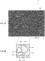
- Figure 2A and Figure 2B shows a distribution of the second region S2 in the cross section SA.
- Figure 2A shows each first region S1 as a black region by applying an image processing (binarization) to the cross section SA of Figure 1 .
- Figure 2B is a schematic redrawn enlargement of a part of Figure 2A .
- first regions S1 are present in the cross section SA of the composite material 10, and these are spaced apart from each other and substantially uniformly distributed. Most of the first regions S1 are surrounded from the outside over the entire circumferences thereof by the second region S2. Further, in at least the range shown in Figure 2B of the cross section SA, the second region S2 is observed as a continuous single region without grain boundaries interposed. That is, in the image obtained by observing at a magnification of 250 times or less as shown in Figure 1 , the presence of grain boundaries that divide this into multiple portions is not observed in the second region S2 shown in Figure 2B .
- granulated powder with higher sphericity and improved fluidity than before is used in the embodiment as a raw material when manufacturing the composite material 10. It is considered that, as a result of silicon carbide, carbon, and the like in the raw materials being dispersed more uniformly than before, the grain growth of silicon carbide occurs, and a continuous second region S2 is formed as in Figure 2B .
- the second region S2 which surrounds the first region S1 from the outside over the entire circumference thereof, is a continuous single region without grain boundaries interposed, as described above, but it is not necessarily a continuous single region in the entirety of the cross section SA shown Figure 1 .
- a plurality of continuous second regions S2 without grain boundaries interposed are present in the cross section SA shown in Figure 1 , and the plurality of second regions S2 may be configured to be adjacent to each other with grain boundaries interposed therebetween.
- the first region S1 with the entire circumference thereof surrounded may be present inside at least one of the second regions S2.
- the second region S2 may be observed as a "continuous single region without grain boundaries interposed" at least when observed with a scanning electron microscope at a magnification of 250 times or less.
- grain boundaries dividing the second region S2 and the corresponding boundaries may be observed.
- FIG. 3A is an image obtained by observing a cross section SB with a scanning electron microscope (SEM), which appears by cutting a composite material 11 according to the comparative example along a plane.
- SEM scanning electron microscope
- the area of the cross section SB is 500 ⁇ m ⁇ 350 ⁇ m at a magnification of 250 times.
- Figure 3B is a schematic redrawn enlargement of a part of Figure 3A .
- the region denoted by a reference numeral "S11” is a region mainly containing silicon like the first region S1 of Figure 2B .
- the region denoted by a reference numeral "S12” is a region mainly containing silicon carbide like the second region S2 of Figure 2B .
- the regions S12 are present as relatively large particles, and a plurality of such particles are present in the cross section SB. Although some of the plurality of regions S12 are in contact with each other, the regions S12 are each separated by a grain boundary. Further, since the regions S12 are relatively large, the regions S11 (silicon) as gaps are each relatively wide and distributed in the form of matrix in the cross section SB. In a part of the cross section SB, the region S11 with its entire circumference surrounded by the region S12 can be present, but the surrounding region S12 is not a single region. That is, there may be a portion where the plurality of regions S12 (silicon carbide) that are adjacent to each other with grain boundaries interposed therebetween are disposed so as to surround the entire circumferences of the regions S11 (silicon).
- the second region S2 is a continuous single region without grain boundaries interposed in the composite material 10 of the embodiment shown in Figure 2A and Figure 2B , and the entire circumferences thereof are surrounded by the second region S2 thereinside, which differs from the comparative example.
- the proportion of the first region S1 in the cross section SA is relatively small.
- silicon contained in the first regions S1 has low strength as compared with silicon carbide contained in the second region S2.
- the proportion of the first regions S1 with low strength is small, and "excessive scraping" during processing is suppressed, precision processing can be performed as compared with before.
- the second region S2 (silicon carbide) that surrounds the first regions S1 is not a collection of multiple particles but is a continuous single region without grain boundaries interposed.
- silicon carbide with a relatively high strength is continuous, "excessive scraping" during processing is further suppressed. Furthermore, it is possible to obtain the effect that particles are less likely to fall off during processing.
- Figure 4 shows the results of an experiment in which the processability of the composite material 10 according to the embodiment is compared with the processability of the composite material 11 according to the comparative example.
- SiC area percentages in the table of Figure 4 shows the area proportions of the regions containing SiC (such as the first regions S1 and the regions S12) in the cross section of each sample as percentages.
- SiC area percentages of the embodiment and the comparative example are each measured in a plurality of cross sections in one sample, and values obtained are shown as areas.
- the image of each cross section as a measurement target is an image with an area of 500 ⁇ m ⁇ 350 ⁇ m at a magnification of 250 times, as in Figure 1 .
- the area of the cross section for measuring the SiC area percentage may be an area wider than above.
- the SiC area percentage was measured in the range of 87.5% to 95.1%.
- the SiC area percentage was measured in the range of 66.2% to 79.1%.
- the second region S2 (or the regions S12) is extracted by applying binarization using an image analysis software to the images of Figure 1 , Figure 3A, and Figure 3B obtained by observation with a scanning electron microscope, to produce an image as in Figure 2A and Figure 2B . Thereafter, using the function of the image analysis software, the total area proportion of the second region S2 (or the regions S12), that is, the SiC area percentage was calculated.
- the "processing depth" in the table of Figure 4 shows, after the surface of each sample is subjected to sandblasting in the same conditions, the measurement results of measuring the depth of the recesses formed on the surface with a gauge in units of mm.
- three portions in one sample of each of the embodiment and the comparative example are subjected to sandblasting, and the processing depth of each portion is measured.
- the "average processing depth” shown in Figure 4 is the average of the three processing depths.
- the composite material 10 according to the embodiment the average processing depth measured was 2.89 mm.
- the composite material 11 according to the comparative example the average processing depth measured was 4.83 mm. In this way, it was confirmed that the composite material 10 according to the embodiment had an average processing depth that is suppressed to smaller as compared with the comparative example and was a material that is easier to perform precision processing.
- the inventors produced a plurality of types of composite materials 10 while changing the manufacturing conditions separately from the embodiment shown in Figure 1 , and each sample was subjected to calculation of the SiC area percentage and measurement of the average processing depth. According to the measurement, it was confirmed that, when the area proportion of the second region S2 in the cross section SA is 70% or more, the average processing depth was reduced, and the processability was sufficiently improved, as compared with before. It was confirmed that, as the area proportion of the second region S2 in the cross section SA increased, the average processing depth was reduced more. When the proportion is 80% or more, the processability was improved remarkably as compared with before. When the proportion is 90% or more (more preferably 95% or more), it was confirmed that the processability was further improved to the extent that fine and highly accurate structures required for semiconductor manufacturing equipment and the like can be formed extremely easily.
- Figure 5 is a diagram showing distribution of the second region S2 in the cross section SA, which is the same image with reference numerals "S1" and "S2" as in Figure 2A .
- the white regions in the circumferences of the first regions S1 generally coincide with the second region S2.
- the second region S2 is observed as a continuous single region without grain boundaries interposed.
- grain boundaries dividing the second region S2 into multiple portions may be observed in the image obtained at a magnification of 250 times or less as in Figure 1 .
- FIG. 6A One of the plurality of first regions S1 in the cross section SA is shown in Figure 6A , and only the first region S1 shown by the arrow AR in Figure 5 is extracted and schematically drawn.
- a diagram in which an inscribed ellipse E corresponding to the first region S1 is superimposed on the same first region S1 as in Figure 6A is shown in Figure 6B .
- the "inscribed ellipse E" is the maximum ellipse that can be disposed fit entirely inside the first region S1.
- the length of each of the major axis MJ and the minor axis MN of the inscribed ellipse E and the ratio thereof can be freely set within a range in which the inscribed ellipse E does not protrude from the first region S1.
- the inscribed ellipse E can also be said to be an ellipse obtained by adjusting the major axis MJ and the minor axis MN so that its area is maximized within a range that does not protrude from the first region S1.
- the shape of the inscribed ellipse E is uniquely determined corresponding to the shape of each first region S1.
- the length of the minor axis MN of the inscribed ellipse E will also be referred to as "L1" below. Furthermore, the length of the major axis MJ of the inscribed ellipse E will also be referred to as "L2" below.
- a graph showing the distribution of L1 can be plotted.
- Such a graph can be plotted, for example, as a histogram shown in Figure 7 .
- the horizontal axis of the graph in Figure 7 represents "classes” that classify the value L1 into predetermined ranges.
- the unit of the numerical value is " ⁇ m”.
- the vertical axis of the graph in Figure 7 represents, for each of the aforementioned classes, the "frequency" of the first region S1 to which L1 belongs to the class, that is, the frequency of L1 in the cross section SA.
- the graph showing the relationship between L1 value and frequency may be plotted as a histogram as shown in Figure 7 , but it may also be plotted as another graph.
- a graph showing the frequency of L1 may be plotted as a continuous curve, such as a normal distribution graph.
- the peak P1 is the peak with the highest frequency in the graph of Figure 7 .
- the peak P1 corresponds to the "first peak” in the graph of Figure 7 .
- the value L1 corresponding to the peak P1 is approximately 1.15 ⁇ m.
- the peak P2 is a peak with the second highest frequency in the graph of Figure 7 .
- Peak P2 corresponds to the "second peak” in the graph of Figure 7 .
- the value L1 corresponding to the peak P2 is about 2.14 ⁇ m. Since the "value L1 corresponding to the peak P2" is defined in the same manner as the "value L1 corresponding to the peak P1" described above, the description thereof is omitted.
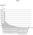
- the length L2 of the major axis MJ of the inscribed ellipse E corresponding to each of the plurality of first regions S1 contained in the cross section SA of Figure 5 is individually calculated, and a graph showing the distribution of L2 can be plotted.
- a graph showing the distribution of L2 can be plotted, for example, as the histogram shown in Figure 8 . Since each of the horizontal axis and the vertical axis of the graph of Figure 8 are defined in the same manner as in Figure 7 , the description thereof is omitted.
- the graph showing the distribution of L2 may also be plotted, for example, as a continuous curve like a normal distribution graph.
- the peak P11 is the peak in the graph with the highest frequency.
- the peak P11 corresponds to the "first peak” in the graph of Figure 8 .
- the value L2 corresponding to the peak P11 is about 2.18 ⁇ m. Since the "value L2 corresponding to the peak P11" is defined as the "value L1 corresponding to the peak P1" described above, the description thereof is omitted.
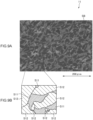
- Figure 9A is an image obtained by observing the cross section SB that appears by cutting the composite material 11 according to the comparative example along a plane with a scanning electron microscope (SEM), which is the same image as in Figure 3A .
- Figure 9B is a schematic redrawn enlargement of a part of Figure 9A .
- the region denoted by the reference numeral "S11” is a region mainly containing silicon like the first region S1 of Figure 5 .
- the region denoted by the reference numeral "S12” is a region mainly containing silicon carbide like the second region S2 of Figure 5 .
- an inscribed ellipse E is drawn for each of the regions S11, and the distribution L1, which is the length of the minor axis MN, and the distribution L2, which is the length of the major axis MJ, can be calculated.
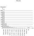
- the graph shown in Figure 10 shows the distribution of L1 in the cross section SB ( Figure 9A and Figure 9B ) in the same manner as in Figure 7 .
- the peak P1 is the peak with the highest frequency in the graph of Figure 10 and corresponds to the "first peak" in the graph.
- the value L1 corresponding to the peak P1 is about 2.33 ⁇ m, which is a value larger than that in the embodiment (1.15 ⁇ m described above).
- the graph shown in Figure 11 shows the distribution of L2 in the cross section SB ( Figure 9A and Figure 9B ) in the same manner as in Figure 8 .
- a single peak P11 appears also in the graph showing the frequency of L2 in this comparative example.
- the peak P11 is the peak with the highest frequency in the graph of Figure 11 and corresponds to the "first peak" in the graph.
- the value L2 corresponding to the peak P11 is about 3.83 ⁇ m, which is a value larger than that in the embodiment (2.18 ⁇ m described above).
- each of the first regions S1 is reduced to the extent that the peak of the distribution of L1 calculated for each of the plurality of first regions S1 in the cross section SA in the composite material 10 of the embodiment is a value less than that in the comparative example.
- the proportion of the first region S1 in the cross section SA is relatively small.
- silicon contained in the first region S1 has a lower strength than silicon carbide contained in the second region S2. Since the proportion of the first regions S1 with low strength is small in the composite material 10, and "excessive scraping" during processing is suppressed, precision processing is enabled as compared with before.
- Figure 12 shows the results of an experiment comparing the processability of the composite material 10 according to the embodiment with the processability of the composite material 11 according to the comparative example.
- the "first peak of the minor axis" in the table of Figure 12 means, when a graph is plotted that shows the distribution of L1 for the cross section of each sample, the value L1 corresponding to the first peak in the graph. That is, it means the value L1 corresponding to the peak P1 in Figure 7 and Figure 10 .
- the unit is " ⁇ m".
- the value L1 corresponding to the peak P1 is calculated for each of a plurality of cross sections in one sample, and each value obtained is shown as the "first peak of the minor axis" as a range.
- the image of each cross section as a measurement target is an image with an area of 500 ⁇ m ⁇ 350 ⁇ m at a magnification of 250 times, as in Figure 1 .
- the area of the cross section used for measuring the distribution of L1 may be wider than above.
- the first peak of the minor axis was calculated in the range of 0.98 ⁇ m to 1.3 ⁇ m. In the embodiment, it was confirmed that the first peak of the minor axis was always within the range of 1.5 ⁇ m or less regardless of how the cross section was taken. Meanwhile, in the composite material 11 according to the comparative example, the first peak of the minor axis was calculated in the range of 0.98 ⁇ m to 8.0 ⁇ m.
- the "second peak of the minor axis" in the table of Figure 12 means, when a graph is plotted that shows the distribution of L1 for the cross section of a sample of the embodiment, the value L1 corresponding to the second peak in the graph. That is, it means the value L1 corresponding to the peak P2 in Figure 7 .
- the unit is " ⁇ m”.
- the value L1 corresponding to the peak P2 is calculated for each of a plurality of cross sections in one sample, and each value obtained is shown as the "second peak of the minor axis" as a range.
- the image of each cross section as a measurement target is the same as the image used for calculating the first peak of the minor axis.
- the second peak of the minor axis was calculated in the range of 1.9 ⁇ m to 2.4 ⁇ m. In the embodiment, it was confirmed that the second peak of the minor axis was always within the range of more than 1.5 ⁇ m and 2.5 ⁇ m or less regardless of how the cross section was taken. In the comparative example, since the second peak did not appear, the "second peak of the minor axis" was not calculated.
- the "first peak of the major axis" in the table of Figure 12 means, when a graph is plotted that shows the distribution of L2 for the cross section of each sample, the value L2 corresponding to the first peak in the graph. That is, it means the value L2 corresponding to the peak P11 in Figure 8 and Figure 11 .
- the unit is " ⁇ m".
- the value L2 corresponding to the peak P11 is calculated for each of a plurality of cross sections in one sample, and each value obtained is shown as the "first peak of the major axis" as a range.
- the image of each cross section as a measurement target is the same as the image used for calculating the first peak of the minor axis or the like.
- the first peak of the major axis was calculated in the range of 1.7 ⁇ m to 2.7 ⁇ m. In the embodiment, it was confirmed that the first peak of the major axis was always within the range of 1.5 ⁇ m or more and 3.0 ⁇ m or less regardless of how the cross section was taken. Meanwhile, in the composite material 11 according to the comparative example, the first peak of the major axis was calculated in the range of 1.1 ⁇ m to 16.0 ⁇ m.
- the "processing depth" in the table of Figure 12 means, when subjecting the surface of each sample to sandblasting in the same conditions and then measuring the depth of recesses formed on the surface with a gauge, the measurement results expressed in the unit of mm.
- three portions in one sample of each of the embodiment and the comparative example are subjected to sandblasting and the processing depth of each portion is measured.
- the "average processing depth” shown in Figure 12 is an average of the three processing depths.
- the average processing depth measured for the composite material 10 according to the embodiment was 2.89 mm.
- the average processing depth measured for the composite material 11 according to the comparative example was 4.83 mm. In this way, the average processing depth of the composite material 10 according to the embodiment is suppressed to small as compared with that of the comparative example, and it was confirmed to be a material that is easier to perform precision processing.
- the inventors produced a plurality of types of composite materials 10 while changing the manufacturing conditions separately from the embodiment shown in Figure 1 or the like, and various indices such as the "first peak of the minor axis" were calculated and the average processing depth was measured for each sample. According to the measurement, it was confirmed that, when the first peak of the minor axis like the peak P1 of Figure 7 was within the range of 1.5 ⁇ m or less, the average processing depth was reduced, and the processability was sufficiently improved as compared with before. Further, it was confirmed that, when the second peak of the minor axis like the peak P2 of Figure 7 appeared in the graph, and it was within the range of more than 1.5 ⁇ m and 2.5 ⁇ m or less, the processability was further improved.
- the processability was improved more remarkably.
- the index that the first peak of the major axis is within the range of 1.5 ⁇ m or more and 3.0 ⁇ m or less can also be used as an index independent of the first peak of the minor axis or the like.
- predetermined amounts of carbon powder and silicon carbide powder as raw materials are each weighed, and dispersed and mixed in pure water together with a binder or a dispersant to produce a slurry.
- the slurry obtained is spray dried using a spray dryer, to produce granulated powder containing carbon and silicon carbide.
- the sphericity of the granulated powder to be obtained can be enhanced by appropriately selecting the binder and the dispersant.
- the target sphericity value is preferably set to a higher value than the sphericity of granulated powder used in conventional SiSiC materials.
- the purpose of increasing the sphericity of the granulated powder is to give the granulated powder sufficient fluidity. It is preferable to increase the fluidity of the granulated powder to an extent that would conventionally be considered excessive.
- the fluidity of the granulated powder varies depending not only on the sphericity of the granulated powder but also on the size of the granulated powder. Therefore, for example, when spray drying a slurry, it is preferable to control the size of the granulated powder by adjusting the flow rate of the supplied air to obtain the granulated powder with optimal fluidity.
- the granulated powder obtained is put into a predetermined mold, and a molded body is obtained by dry uniaxial press molding.
- the granulated powder is packed sufficiently densely into the mold by increasing the fluidity of the granulated powder in advance as described above. As a result, a molded body with small pore diameters can be obtained.
- molding may be performed using CIP (Cold Isostatic Pressing) or may be performed by a method of modeling while spreading powder using a 3D printer.
- CIP Cold Isostatic Pressing
- metal silicon is placed on the molded body and fired under reduced pressure.
- the composite material 10 as shown in Figure 1 or the like can be obtained impregnating the molded body with molten silicon and performing reaction sintering with carbon powder.
- the fluidity of the granulated powder is increased than before, and a molded body is obtained while being sufficiently densely packed in the mold, as described above.
- a single continuous second region S2 is formed over a relatively wide range as described above, the second region S2 is formed over a relatively wide range, and the first region S1 becomes smaller than before.
- predetermined amounts of carbon powder and silicon carbide powder were each weighed first, and then dispersed and mixed in pure water together with a binder or a dispersant, to produce a slurry. Thereafter, the slurry obtained was cast into a plaster mold, to obtain a molded body by cast molding. After the completion of molding, metal silicon was placed on the molded body obtained and then fired under reduced pressure.
Landscapes
- Chemical & Material Sciences (AREA)
- Engineering & Computer Science (AREA)
- Ceramic Engineering (AREA)
- Manufacturing & Machinery (AREA)
- Materials Engineering (AREA)
- Structural Engineering (AREA)
- Organic Chemistry (AREA)
- Inorganic Chemistry (AREA)
- Chemical Kinetics & Catalysis (AREA)
- Ceramic Products (AREA)
Applications Claiming Priority (2)
| Application Number | Priority Date | Filing Date | Title |
|---|---|---|---|
| JP2023015171A JP7705900B2 (ja) | 2023-02-03 | 2023-02-03 | 複合材料 |
| JP2023015172A JP7768915B2 (ja) | 2023-02-03 | 2023-02-03 | 複合材料 |
Publications (1)
| Publication Number | Publication Date |
|---|---|
| EP4474366A1 true EP4474366A1 (de) | 2024-12-11 |
Family
ID=89723212
Family Applications (1)
| Application Number | Title | Priority Date | Filing Date |
|---|---|---|---|
| EP24154022.8A Pending EP4474366A1 (de) | 2023-02-03 | 2024-01-25 | Verbundmaterial |
Country Status (1)
| Country | Link |
|---|---|
| EP (1) | EP4474366A1 (de) |
Citations (3)
| Publication number | Priority date | Publication date | Assignee | Title |
|---|---|---|---|---|
| JPH0648837A (ja) * | 1992-07-24 | 1994-02-22 | Shin Etsu Chem Co Ltd | 半導体製造用炭化珪素質部材 |
| US20010003620A1 (en) * | 1998-12-11 | 2001-06-14 | Dominique Dubots | High purity, siliconized silicon carbide having high thermal shock resistance |
| JP2001348288A (ja) | 2000-06-05 | 2001-12-18 | Toshiba Corp | 粒子分散シリコン材料およびその製造方法 |
-
2024
- 2024-01-25 EP EP24154022.8A patent/EP4474366A1/de active Pending
Patent Citations (3)
| Publication number | Priority date | Publication date | Assignee | Title |
|---|---|---|---|---|
| JPH0648837A (ja) * | 1992-07-24 | 1994-02-22 | Shin Etsu Chem Co Ltd | 半導体製造用炭化珪素質部材 |
| US20010003620A1 (en) * | 1998-12-11 | 2001-06-14 | Dominique Dubots | High purity, siliconized silicon carbide having high thermal shock resistance |
| JP2001348288A (ja) | 2000-06-05 | 2001-12-18 | Toshiba Corp | 粒子分散シリコン材料およびその製造方法 |
Non-Patent Citations (2)
| Title |
|---|
| WAHL LARISSA ET AL: "Robocasting of reaction bonded silicon carbide structures", JOURNAL OF THE EUROPEAN CERAMIC SOCIETY, ELSEVIER, AMSTERDAM, NL, vol. 39, no. 15, 27 June 2019 (2019-06-27), pages 4520 - 4526, XP085810498, ISSN: 0955-2219, [retrieved on 20190627], DOI: 10.1016/J.JEURCERAMSOC.2019.06.049 * |
| ZHANG NAN-LONG ET AL: "Preparation and properties of reaction bonded silicon carbide (RB-SiC) ceramics with high SiC percentage by two-step sintering using compound carbon sources", CERAMICS INTERNATIONAL, vol. 45, no. 12, 30 April 2019 (2019-04-30), pages 15715 - 15719, XP085707582, ISSN: 0272-8842, DOI: 10.1016/J.CERAMINT.2019.04.224 * |
Similar Documents
| Publication | Publication Date | Title |
|---|---|---|
| DE112009000724B4 (de) | Ziegelsteinplatte und Verfahren zu ihrer Herstellung | |
| EP3380324A1 (de) | 3d drucken von einem keramischen bauteil | |
| CN108290353A (zh) | 用于熔融金属或玻璃的成型工具 | |
| JP5277483B2 (ja) | 黒鉛材料 | |
| DE69808418T2 (de) | Verfahren zur Herstellung von whiskerverstärkten Keramiken | |
| EP1238953A1 (de) | Verbundwerkstoff auf der Basis von Siliciumcarbid und Kohlenstoff, Verfahren zu seiner Herstellung sowie seine Verwendung | |
| EP4613724A1 (de) | Verbundmaterial | |
| EP4474366A1 (de) | Verbundmaterial | |
| DE69213288T2 (de) | Einsatzstücke bevorzugt zum bearbeiten von hitzefesten Materialien und Verfahren zu ihrer Herstellung. | |
| KR101773130B1 (ko) | 수축률이 감소한 치아 가공용 지르코니아 블록의 제조방법 | |
| Hotta et al. | Origin of strength change in ceramics associated with the alteration of spray dryer | |
| JP7768915B2 (ja) | 複合材料 | |
| JP2010222155A (ja) | 炭化珪素質焼結体及びその製造方法 | |
| DE60307777T2 (de) | Werkzeugeinsatz und zugehöriges Herstellungsverfahren | |
| JP7705900B2 (ja) | 複合材料 | |
| JPH0798684B2 (ja) | 高密度SiC焼結体の製造方法 | |
| KR20240076797A (ko) | 복합 마모 부품 | |
| WO2023190467A1 (ja) | セラミックスボール用素材およびそれを用いたセラミックスボールの製造方法並びにセラミックスボール | |
| JP6680605B2 (ja) | 焼成用容器の製造方法 | |
| JP7068657B2 (ja) | 立方晶窒化ほう素基焼結体製切削工具 | |
| JP2026004871A (ja) | 複合材料 | |
| EP3380445A1 (de) | Kohlenstoff-metall verbundwerkstoff | |
| JP2026004870A (ja) | 複合材料 | |
| RU2767129C1 (ru) | Гильза цилиндра для литья с закладными элементами | |
| KR102448644B1 (ko) | 철계 소결 합금 및 그 제조 방법 |
Legal Events
| Date | Code | Title | Description |
|---|---|---|---|
| PUAI | Public reference made under article 153(3) epc to a published international application that has entered the european phase |
Free format text: ORIGINAL CODE: 0009012 |
|
| STAA | Information on the status of an ep patent application or granted ep patent |
Free format text: STATUS: REQUEST FOR EXAMINATION WAS MADE |
|
| 17P | Request for examination filed |
Effective date: 20240126 |
|
| AK | Designated contracting states |
Kind code of ref document: A1 Designated state(s): AL AT BE BG CH CY CZ DE DK EE ES FI FR GB GR HR HU IE IS IT LI LT LU LV MC ME MK MT NL NO PL PT RO RS SE SI SK SM TR |