EP4468324A2 - Integrated circuit substrate for containing liquid adhesive bleed-out - Google Patents
Integrated circuit substrate for containing liquid adhesive bleed-out Download PDFInfo
- Publication number
- EP4468324A2 EP4468324A2 EP24205880.8A EP24205880A EP4468324A2 EP 4468324 A2 EP4468324 A2 EP 4468324A2 EP 24205880 A EP24205880 A EP 24205880A EP 4468324 A2 EP4468324 A2 EP 4468324A2
- Authority
- EP
- European Patent Office
- Prior art keywords
- integrated circuit
- substrate layer
- circuit die
- top surface
- trench
- Prior art date
- Legal status (The legal status is an assumption and is not a legal conclusion. Google has not performed a legal analysis and makes no representation as to the accuracy of the status listed.)
- Pending
Links
Images



Classifications
-
- H—ELECTRICITY
- H10—SEMICONDUCTOR DEVICES; ELECTRIC SOLID-STATE DEVICES NOT OTHERWISE PROVIDED FOR
- H10W—GENERIC PACKAGES, INTERCONNECTIONS, CONNECTORS OR OTHER CONSTRUCTIONAL DETAILS OF DEVICES COVERED BY CLASS H10
- H10W74/00—Encapsulations, e.g. protective coatings
- H10W74/40—Encapsulations, e.g. protective coatings characterised by their materials
- H10W74/47—Encapsulations, e.g. protective coatings characterised by their materials comprising organic materials, e.g. plastics or resins
-
- H—ELECTRICITY
- H10—SEMICONDUCTOR DEVICES; ELECTRIC SOLID-STATE DEVICES NOT OTHERWISE PROVIDED FOR
- H10W—GENERIC PACKAGES, INTERCONNECTIONS, CONNECTORS OR OTHER CONSTRUCTIONAL DETAILS OF DEVICES COVERED BY CLASS H10
- H10W70/00—Package substrates; Interposers; Redistribution layers [RDL]
- H10W70/60—Insulating or insulated package substrates; Interposers; Redistribution layers
- H10W70/67—Insulating or insulated package substrates; Interposers; Redistribution layers characterised by their insulating layers or insulating parts
- H10W70/68—Shapes or dispositions thereof
-
- H—ELECTRICITY
- H10—SEMICONDUCTOR DEVICES; ELECTRIC SOLID-STATE DEVICES NOT OTHERWISE PROVIDED FOR
- H10W—GENERIC PACKAGES, INTERCONNECTIONS, CONNECTORS OR OTHER CONSTRUCTIONAL DETAILS OF DEVICES COVERED BY CLASS H10
- H10W70/00—Package substrates; Interposers; Redistribution layers [RDL]
- H10W70/60—Insulating or insulated package substrates; Interposers; Redistribution layers
- H10W70/611—Insulating or insulated package substrates; Interposers; Redistribution layers for connecting multiple chips together
-
- H—ELECTRICITY
- H10—SEMICONDUCTOR DEVICES; ELECTRIC SOLID-STATE DEVICES NOT OTHERWISE PROVIDED FOR
- H10W—GENERIC PACKAGES, INTERCONNECTIONS, CONNECTORS OR OTHER CONSTRUCTIONAL DETAILS OF DEVICES COVERED BY CLASS H10
- H10W70/00—Package substrates; Interposers; Redistribution layers [RDL]
- H10W70/60—Insulating or insulated package substrates; Interposers; Redistribution layers
- H10W70/62—Insulating or insulated package substrates; Interposers; Redistribution layers characterised by their interconnections
- H10W70/65—Shapes or dispositions of interconnections
-
- H—ELECTRICITY
- H10—SEMICONDUCTOR DEVICES; ELECTRIC SOLID-STATE DEVICES NOT OTHERWISE PROVIDED FOR
- H10W—GENERIC PACKAGES, INTERCONNECTIONS, CONNECTORS OR OTHER CONSTRUCTIONAL DETAILS OF DEVICES COVERED BY CLASS H10
- H10W70/00—Package substrates; Interposers; Redistribution layers [RDL]
- H10W70/60—Insulating or insulated package substrates; Interposers; Redistribution layers
- H10W70/67—Insulating or insulated package substrates; Interposers; Redistribution layers characterised by their insulating layers or insulating parts
- H10W70/68—Shapes or dispositions thereof
- H10W70/685—Shapes or dispositions thereof comprising multiple insulating layers
-
- H—ELECTRICITY
- H10—SEMICONDUCTOR DEVICES; ELECTRIC SOLID-STATE DEVICES NOT OTHERWISE PROVIDED FOR
- H10W—GENERIC PACKAGES, INTERCONNECTIONS, CONNECTORS OR OTHER CONSTRUCTIONAL DETAILS OF DEVICES COVERED BY CLASS H10
- H10W74/00—Encapsulations, e.g. protective coatings
- H10W74/01—Manufacture or treatment
- H10W74/012—Manufacture or treatment of encapsulations on active surfaces of flip-chip devices, e.g. forming underfills
-
- H—ELECTRICITY
- H10—SEMICONDUCTOR DEVICES; ELECTRIC SOLID-STATE DEVICES NOT OTHERWISE PROVIDED FOR
- H10W—GENERIC PACKAGES, INTERCONNECTIONS, CONNECTORS OR OTHER CONSTRUCTIONAL DETAILS OF DEVICES COVERED BY CLASS H10
- H10W74/00—Encapsulations, e.g. protective coatings
- H10W74/10—Encapsulations, e.g. protective coatings characterised by their shape or disposition
- H10W74/131—Encapsulations, e.g. protective coatings characterised by their shape or disposition the semiconductor body being only partially enclosed
- H10W74/141—Encapsulations, e.g. protective coatings characterised by their shape or disposition the semiconductor body being only partially enclosed the encapsulations being on at least the sidewalls of the semiconductor body
-
- H—ELECTRICITY
- H10—SEMICONDUCTOR DEVICES; ELECTRIC SOLID-STATE DEVICES NOT OTHERWISE PROVIDED FOR
- H10W—GENERIC PACKAGES, INTERCONNECTIONS, CONNECTORS OR OTHER CONSTRUCTIONAL DETAILS OF DEVICES COVERED BY CLASS H10
- H10W74/00—Encapsulations, e.g. protective coatings
- H10W74/10—Encapsulations, e.g. protective coatings characterised by their shape or disposition
- H10W74/15—Encapsulations, e.g. protective coatings characterised by their shape or disposition on active surfaces of flip-chip devices, e.g. underfills
-
- H—ELECTRICITY
- H10—SEMICONDUCTOR DEVICES; ELECTRIC SOLID-STATE DEVICES NOT OTHERWISE PROVIDED FOR
- H10W—GENERIC PACKAGES, INTERCONNECTIONS, CONNECTORS OR OTHER CONSTRUCTIONAL DETAILS OF DEVICES COVERED BY CLASS H10
- H10W90/00—Package configurations
- H10W90/401—Package configurations characterised by multiple insulating or insulated package substrates, interposers or RDLs
-
- H—ELECTRICITY
- H10—SEMICONDUCTOR DEVICES; ELECTRIC SOLID-STATE DEVICES NOT OTHERWISE PROVIDED FOR
- H10W—GENERIC PACKAGES, INTERCONNECTIONS, CONNECTORS OR OTHER CONSTRUCTIONAL DETAILS OF DEVICES COVERED BY CLASS H10
- H10W90/00—Package configurations
- H10W90/701—Package configurations characterised by the relative positions of pads or connectors relative to package parts
-
- H—ELECTRICITY
- H10—SEMICONDUCTOR DEVICES; ELECTRIC SOLID-STATE DEVICES NOT OTHERWISE PROVIDED FOR
- H10W—GENERIC PACKAGES, INTERCONNECTIONS, CONNECTORS OR OTHER CONSTRUCTIONAL DETAILS OF DEVICES COVERED BY CLASS H10
- H10W70/00—Package substrates; Interposers; Redistribution layers [RDL]
- H10W70/60—Insulating or insulated package substrates; Interposers; Redistribution layers
- H10W70/67—Insulating or insulated package substrates; Interposers; Redistribution layers characterised by their insulating layers or insulating parts
- H10W70/68—Shapes or dispositions thereof
- H10W70/682—Shapes or dispositions thereof comprising holes having chips therein
-
- H—ELECTRICITY
- H10—SEMICONDUCTOR DEVICES; ELECTRIC SOLID-STATE DEVICES NOT OTHERWISE PROVIDED FOR
- H10W—GENERIC PACKAGES, INTERCONNECTIONS, CONNECTORS OR OTHER CONSTRUCTIONAL DETAILS OF DEVICES COVERED BY CLASS H10
- H10W72/00—Interconnections or connectors in packages
- H10W72/071—Connecting or disconnecting
- H10W72/073—Connecting or disconnecting of die-attach connectors
- H10W72/07331—Connecting techniques
- H10W72/07337—Connecting techniques using a polymer adhesive, e.g. an adhesive based on silicone or epoxy
- H10W72/07338—Connecting techniques using a polymer adhesive, e.g. an adhesive based on silicone or epoxy hardening the adhesive by curing, e.g. thermosetting
-
- H—ELECTRICITY
- H10—SEMICONDUCTOR DEVICES; ELECTRIC SOLID-STATE DEVICES NOT OTHERWISE PROVIDED FOR
- H10W—GENERIC PACKAGES, INTERCONNECTIONS, CONNECTORS OR OTHER CONSTRUCTIONAL DETAILS OF DEVICES COVERED BY CLASS H10
- H10W72/00—Interconnections or connectors in packages
- H10W72/20—Bump connectors, e.g. solder bumps or copper pillars; Dummy bumps; Thermal bumps
- H10W72/251—Materials
- H10W72/252—Materials comprising solid metals or solid metalloids, e.g. PbSn, Ag or Cu
-
- H—ELECTRICITY
- H10—SEMICONDUCTOR DEVICES; ELECTRIC SOLID-STATE DEVICES NOT OTHERWISE PROVIDED FOR
- H10W—GENERIC PACKAGES, INTERCONNECTIONS, CONNECTORS OR OTHER CONSTRUCTIONAL DETAILS OF DEVICES COVERED BY CLASS H10
- H10W72/00—Interconnections or connectors in packages
- H10W72/30—Die-attach connectors
- H10W72/351—Materials of die-attach connectors
- H10W72/353—Materials of die-attach connectors not comprising solid metals or solid metalloids, e.g. ceramics
- H10W72/354—Materials of die-attach connectors not comprising solid metals or solid metalloids, e.g. ceramics comprising polymers
-
- H—ELECTRICITY
- H10—SEMICONDUCTOR DEVICES; ELECTRIC SOLID-STATE DEVICES NOT OTHERWISE PROVIDED FOR
- H10W—GENERIC PACKAGES, INTERCONNECTIONS, CONNECTORS OR OTHER CONSTRUCTIONAL DETAILS OF DEVICES COVERED BY CLASS H10
- H10W72/00—Interconnections or connectors in packages
- H10W72/30—Die-attach connectors
- H10W72/381—Auxiliary members
- H10W72/387—Flow barriers
-
- H—ELECTRICITY
- H10—SEMICONDUCTOR DEVICES; ELECTRIC SOLID-STATE DEVICES NOT OTHERWISE PROVIDED FOR
- H10W—GENERIC PACKAGES, INTERCONNECTIONS, CONNECTORS OR OTHER CONSTRUCTIONAL DETAILS OF DEVICES COVERED BY CLASS H10
- H10W72/00—Interconnections or connectors in packages
- H10W72/851—Dispositions of multiple connectors or interconnections
- H10W72/874—On different surfaces
- H10W72/877—Bump connectors and die-attach connectors
-
- H—ELECTRICITY
- H10—SEMICONDUCTOR DEVICES; ELECTRIC SOLID-STATE DEVICES NOT OTHERWISE PROVIDED FOR
- H10W—GENERIC PACKAGES, INTERCONNECTIONS, CONNECTORS OR OTHER CONSTRUCTIONAL DETAILS OF DEVICES COVERED BY CLASS H10
- H10W90/00—Package configurations
-
- H—ELECTRICITY
- H10—SEMICONDUCTOR DEVICES; ELECTRIC SOLID-STATE DEVICES NOT OTHERWISE PROVIDED FOR
- H10W—GENERIC PACKAGES, INTERCONNECTIONS, CONNECTORS OR OTHER CONSTRUCTIONAL DETAILS OF DEVICES COVERED BY CLASS H10
- H10W90/00—Package configurations
- H10W90/20—Configurations of stacked chips
- H10W90/24—Configurations of stacked chips at least one of the stacked chips being laterally offset from a neighbouring stacked chip, e.g. chip stacks having a staircase shape
-
- H—ELECTRICITY
- H10—SEMICONDUCTOR DEVICES; ELECTRIC SOLID-STATE DEVICES NOT OTHERWISE PROVIDED FOR
- H10W—GENERIC PACKAGES, INTERCONNECTIONS, CONNECTORS OR OTHER CONSTRUCTIONAL DETAILS OF DEVICES COVERED BY CLASS H10
- H10W90/00—Package configurations
- H10W90/701—Package configurations characterised by the relative positions of pads or connectors relative to package parts
- H10W90/721—Package configurations characterised by the relative positions of pads or connectors relative to package parts of bump connectors
- H10W90/722—Package configurations characterised by the relative positions of pads or connectors relative to package parts of bump connectors between stacked chips
-
- H—ELECTRICITY
- H10—SEMICONDUCTOR DEVICES; ELECTRIC SOLID-STATE DEVICES NOT OTHERWISE PROVIDED FOR
- H10W—GENERIC PACKAGES, INTERCONNECTIONS, CONNECTORS OR OTHER CONSTRUCTIONAL DETAILS OF DEVICES COVERED BY CLASS H10
- H10W90/00—Package configurations
- H10W90/701—Package configurations characterised by the relative positions of pads or connectors relative to package parts
- H10W90/721—Package configurations characterised by the relative positions of pads or connectors relative to package parts of bump connectors
- H10W90/724—Package configurations characterised by the relative positions of pads or connectors relative to package parts of bump connectors between a chip and a stacked insulating package substrate, interposer or RDL
-
- H—ELECTRICITY
- H10—SEMICONDUCTOR DEVICES; ELECTRIC SOLID-STATE DEVICES NOT OTHERWISE PROVIDED FOR
- H10W—GENERIC PACKAGES, INTERCONNECTIONS, CONNECTORS OR OTHER CONSTRUCTIONAL DETAILS OF DEVICES COVERED BY CLASS H10
- H10W90/00—Package configurations
- H10W90/701—Package configurations characterised by the relative positions of pads or connectors relative to package parts
- H10W90/731—Package configurations characterised by the relative positions of pads or connectors relative to package parts of die-attach connectors
- H10W90/734—Package configurations characterised by the relative positions of pads or connectors relative to package parts of die-attach connectors between a chip and a stacked insulating package substrate, interposer or RDL
Definitions
- Certain integrated devices can be fabricated by bonding an integrated circuit in a cavity of a substrate.
- the cavity can be formed by joining two substrate layers with an adhesive, and then cutting away a portion of one layer.
- additional components can be bonded across both a top surface of the substrate and a top surface of the integrated circuit.
- At least one aspect is directed to a device including a first substrate layer having a top surface and a bottom surface.
- the device includes a second substrate layer having a bottom surface adhered to a first portion of the top surface of the first substrate layer such that a second portion of the top surface of the first substrate layer is exposed to define a bottom of a cavity, and n edge of the second substrate layer adjacent to the exposed top surface of the first substrate layer defines an edge of the cavity.
- the device includes an integrated circuit die adhered to the exposed top surface of first substrate layer with a liquid adhesive.
- the first substrate layer defines a trench in the bottom of the cavity between a region of the integrated circuit die and the edge of the cavity such that the trench can receive bleed-out of the liquid adhesive from between the integrated circuit die and the top surface of the first substrate layer.
- At least one aspect is directed to a method of fabricating a device.
- the method includes providing a first substrate layer having a top surface and a bottom surface.
- the method includes adhering a bottom surface of a second substrate layer to the top surface of the first substrate layer.
- the method includes removing a portion of the second substrate layer to expose a portion of the top surface of the first substrate layer.
- the method includes cutting a trench into the exposed portion of the top surface of the first substrate layer.
- the method includes adhering an integrated circuit die onto the exposed top surface of the first substrate layer with a liquid adhesive such that the trench receives bleed-out of the liquid adhesive from between the integrated circuit die and the top surface of the first substrate layer.
- This disclosure generally relates to an integrated circuit substrate for containing liquid adhesive bleed-out and a method for fabricating the same.
- Certain integrated devices can be fabricated by bonding an integrated circuit in a cavity of a substrate.
- the cavity can be formed by joining two substrate layers with an adhesive, and then cutting away a portion of the second layer.
- the cutting can be performed by a laser.
- the laser may scorch or otherwise degrade the adhesive, which is typically an organic compound.
- the burned adhesive may form burrs. These burrs may interfere with placement of the integrated circuit die within the cavity.
- the burr may get caught underneath the die, preventing the die from seating properly.
- the die may be tilted and thus have uneven contact with the cavity surface. In extreme cases, the burr may cause a gap to form between the die and the substrate.
- the gap can be vulnerable to particle contamination due to dust in air circulating in the vicinity of the integrated device.
- the die can be bonded to the substrate using an epoxy or other liquid adhesive.
- an epoxy or other liquid adhesive In high-volume production, it may be difficult to control the amount of liquid adhesive used to bond the die to the substrate. Too little liquid adhesive may result in a poorly bonded device vulnerable to mechanical failures. Too much liquid adhesive, however, may contaminate surfaces of the die and/or the substrate that need to remain clear following the bonding steps. Too much liquid adhesive may also create a large fillet that may interfere with the placement of other components in the cavity or otherwise in the vicinity of the die.
- One or more trenches can be machined, etched, or otherwise cut into the floor of the cavity; i.e., into a surface of the first substrate layer.
- the one or more trenches can be formed in a region outside a perimeter of the die, within the perimeter of the die, or straddling the perimeter of the die.
- the trench can be formed in the first substrate layer following formation of the cavity.
- the cutting of the trench itself may remove any burrs that could have interfered with placement and bonding of the die.
- any burrs remaining following the trench-cutting steps may be pushed into the trench and thus prevented from interfering with the placement of the die.
- the one or more trenches can provide an overflow region for excess liquid adhesive.
- the one or more trenches can divert and collect excess liquid adhesive, and prevent the excess liquid adhesive from fouling or otherwise obscuring surfaces of the die or substrate that need to remain clear following the die bonding steps.
- the one or more trenches can also prevent the fillet from extending too far from the perimeter of the die and obstructing components that need to be placed adjacent to the die. In this manner, two dies can be placed in closer proximity than previously possible without the trench features while still allowing for liquid adhesive volume tolerance variations typical of high production volume processes.
- Figure 1 illustrates an integrated device 100 having an integrated circuit die 140 mounted in a cavity 130 of a substrate 110 and 120 with a burr and regions of liquid adhesive overflow.
- the finished substrate shown in the device 100 includes a first substrate layer 120 and a second substrate layer 110.
- the second substrate layer 110 is adhered to the first substrate layer 120 with an adhesive.
- the adhesive is an organic compound.
- a portion of the second substrate layer 110 is either absent or removed to expose a portion of a top surface of the first substrate layer 120 and define the cavity 130.
- the portion of the second substrate layer 110 is removed by cutting through the second substrate layer with a cutting laser. During the cutting process, the laser may scorch, burn, or otherwise affect the adhesive in a manner that can produce debris in the form of burrs.
- the burrs can interfere with subsequent fabrication steps, such as adhering the integrated circuit die 140 to the substrate.
- a burr may get lodged underneath the integrated circuit die 140 and prevent it from seating properly; that is, cause it to mount with a tilt.
- the tilt may cause problems for mounting additional components to the integrated circuit die 140, including components that may be mounted in a manner that spans both the integrated circuit die 140 and a top surface of the second substrate layer 110.
- the tilt may also result in voids between the integrated circuit die 140 and the substrate.
- the voids can become contaminated later in the fabrication process or following deployment of the device 100.
- the void may fill with dust or other contaminants in a manner that detrimentally affects operation of the device 100, such as reducing performance or causing intermittent or early an unrepairable failures.
- the integrated circuit die 140 is adhered to the exposed top surface of the first substrate layer 120 with a liquid adhesive, which may be an epoxy.
- a liquid adhesive which may be an epoxy.
- the amount of liquid adhesive used will vary within a tolerance range. The nominal amount of liquid adhesive used may be set to make sure that even at the low end of the tolerance range, enough is used to create an adequate bond.
- the device 100 may experience bleed-out or overflow of the liquid adhesive out from under the integrated circuit die 140. The bleed-out can cause various problems, such as fouling or obscuring regions of the device 100 that need to remain exposed during subsequent fabrication steps and/or after deployment.
- the bleed-out, once hardened can obstruct placement of other components adjacent to the integrated circuit die 140.
- a second integrated circuit die may be placed close to the first integrated circuit die 140 such that the two can be connected.
- the nature of the connection or of the shared functions between the two dies may require close proximity between them, a close proximity that may be prevented by a fillet or blob of hardened/cured liquid adhesive extending an excessive distance away from the first integrated circuit die 140.
- this disclosure describes creating trench features in the exposed top surface of the first substrate layer 120.
- the trenches can receive burrs caused by cutting the second substrate layer 110; and, in some cases, the act of cutting of the trenches itself may remove burrs before they can interfere with subsequent fabrication steps.
- the trenches can also receive liquid adhesive bleed-out and prevent excessive bleed-out from fouling the device 100 or obstructing the placement of additional components.
- Figure 2 illustrates a first example integrated device 200 having an integrated circuit die 240 mounted in a cavity 230 of a substrate 210 and 220 with trenches 260a and 260b outside the perimeter of the integrated circuit die for containing liquid adhesive bleed-out.
- the device 200 includes a first substrate layer 220 and a second substrate layer 210. A portion of the second substrate layer 210 has been removed to expose a portion of a top surface of the first substrate layer 220 and define the cavity 230.
- the trenches 260a and 260b (collectively "trenches 260") have been cut, etched, machined, or otherwise defined into the top surface of the first substrate layer 220 in a region near the intended position of the integrated circuit die 240.
- the trenches 260 can be configured to receive any burrs or other debris left over from the process of cutting the second substrate layer 210. In some cases, the process of cutting the trenches 260 can remove debris proactively. In addition, the trenches 260 can be configured to receive any bleed-out of a liquid adhesive used to adhere the integrated circuit die 240 to the exposed top surface of the first substrate layer 220.
- the trenches 260 are shown positioned outside of a perimeter of the integrated circuit die 240.
- the trenches 260 can be defined such that they align with the perimeter of the integrated circuit die 240, extend across the perimeter of the integrated circuit die 240, or lie completely within the perimeter of the integrated circuit die 240.
- Figure 3 illustrates a second example integrated device 300 having an integrated circuit die 240 mounted in a cavity 230 of a substrate 220 and 210 with trenches 360a and 360b aligned with a perimeter of the integrated circuit die 240 for containing liquid adhesive bleed-out, and additionally having a bridge die 350 mounted over the integrated circuit die 240 and substrate220 and 210.
- the first substrate layer 220, second substrate layer 210, cavity 230, and integrated circuit die 240 can be similar to the corresponding features of the device 200 previously described.
- the trenches 360a and 360b are aligned with the perimeter of the integrated circuit die 240.
- the device 300 additionally has a bridge die 350 mounted across the first substrate layer and the integrated circuit die 240.
- the bridge die 350 can have solder balls 370 for mechanically and electrically coupling the bridge die 350 to the second substrate layer and the integrated circuit die 240.
- the trenches 360 can prevent a burr from interfering with proper placement of the integrated circuit die 240, which could result in a tilt that could prevent proper positioning of the bridge die 350.
- the trenches 360 can further prevent bleed-out of the liquid adhesive from fouling a region between the integrated circuit die 240 and an edge of the second adhesive layer 210 in a manner that could interfere with placement of the bridge die 350.
- Figure 4 illustrates a third example integrated device 400 having an integrated circuit die 440 mounted in a cavity 430 of a substrate 420 and 410 with a trench 460 slightly incut from a perimeter of the integrated circuit die 440 for containing liquid adhesive bleed-out.
- the first substrate layer 420, second substrate layer 410, cavity 430, integrated circuit die 440, and bridge die 450 can be similar to the first substrate layer 220, second substrate layer 210, cavity 230, integrated circuit die 240, and bridge die 350, respectively of the device 300 previously described.
- the trench 460 extends across the perimeter of the integrated circuit die 440; i.e., the trench 460 is slightly incut from the edge of the integrated circuit die 440.
- a slightly incut trench can further reduce the extent of the fillet of the liquid adhesive bleed-out from the side of the integrated circuit device 440 and avoid any interference with additional components that need to be positioned adjacent to the integrated circuit device 440.
- Figure 5 below illustrates the placement of such an adjacent component.
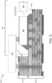
- Figure 5 illustrates a fourth example integrated device 500 having an integrated circuit die 540 mounted in a cavity 530 of a substrate 520 and 510 with a trench 560 straddling a perimeter of the integrated circuit die 540 for containing liquid adhesive bleed-out.
- the first substrate layer 520, second substrate layer 510, cavity 530, integrated circuit die 540, and bridge die 550 can be similar to the first substrate layer 220, second substrate layer 210, cavity 230, integrated circuit die 240, and bridge die 350, respectively of the device 300 previously described.
- the trench 560 extends across the perimeter of the integrated circuit die 540; i.e., the trench 460 straddles the edge of the integrated circuit die 440.
- the position of the trench 560 relative to the edge of the integrated circuit die 540 can reduce the extent of the fillet of the liquid adhesive bleed-out from the side of the integrated circuit device 540 and prevent interference with an additional component that needs to be positioned adjacent to the integrated circuit device 540, such as the second integrated circuit die 545.
- the trench 560 can be positioned such that it straddles the perimeters of both integrated circuit dies 540 and 545.
- the trench 560 can therefore receive any liquid adhesive bleed-out from either or both of the integrated circuit dies 540 and 545.
- the trench 560 can thus prevent excess liquid adhesive from fouling the region between (or, in some cases, above) the integrated circuit dies 540 and 545. Accordingly, excess liquid adhesive can be prevented from interfering with any interconnects or additional components that may need to be positioned across or between the integrated circuit dies 540 and 545.
- FIG. 6 is a flowchart of an example method 600 of fabricating an integrated device having means for containing liquid adhesive-bleed out, according to an example implementation.
- the method 600 is suitable for fabricating an integrated device similar to the devices 200, 300, 400, or 500 previously described.
- the method 600 includes providing a first substrate layer (stage 610).
- the method 600 includes adhering a second substrate layer to a top surface of the first substrate layer (stage 620).
- the method 600 includes removing a portion of the second substrate layer to expose a portion of the top surface of the first substrate layer (stage 630).
- the method 600 includes cutting a trench into the exposed portion of the top surface of the first substrate layer (stage 640).
- the method 600 includes adhering an integrated circuit die onto the exposed top surface of the first substrate layer (stage 650).
- the method 600 can optionally include cutting a second trench into the exposed portion of the top surface of the first substrate layer (stage 660) and adhering a second integrated circuit die adjacent to the first integrated circuit die (stage 670). In some implementations, the method 600 can optionally include mounting a bridge die over a portion of the second substrate layer and a portion of the integrated circuit die (stage (680).
- the method 600 is suitable for fabricating an integrated device similar to the devices 200, 300, 400, or 500 previously described.
- the method 600 includes providing a first substrate layer (stage 610).
- the first substrate layer can be similar to the first substrate layer 220, 420, or 520 previously described.
- the method 600 includes adhering a second substrate layer to a top surface of the first substrate layer (stage 620).
- the second substrate layer can be similar to the second substrate layer 210, 410, or 510 previously described.
- a bottom surface of the second substrate layer can be adhered to a top surface of the first substrate layer using an adhesive.
- the adhesive can include an organic compound.
- the method 600 includes removing a portion of the second substrate layer to expose a portion of the top surface of the first substrate layer (stage 630).
- a portion of the second substrate layer can be cut and removed to expose a portion of the top surface of the first substrate layer.
- the cut can be made with a laser, blade, bit, mill, or chemical process. Removal of the portion of the second substrate layer can form a cavity defined on the side by an edge of the second substrate layer exposed by the cut, and on the bottom by the exposed top surface of the first substrate layer.
- the cavity can be similar to the cavities 230, 430, or 530 previously described.
- the cutting process may leave behind a residue or debris of either the substrate material or the adhesive.
- the debris can take the form of a burr consisting of burned or scorched material. If not remove, the burr may interfere with subsequent fabrication stages, such as placement of an integrated circuit die or other components within the cavity.
- the method 600 includes cutting a trench into the exposed portion of the top surface of the first substrate layer (stage 640).
- the trench can be similar to the trenches 260, 360, 460, or 560 previously described.
- the trench can be cut with a laser, blade, bit, mill, or chemical process.
- the process for cutting the trench can be similar to the process for cutting the second substrate layer to create the cavity.
- the cutting process may remove any burrs or other debris remaining from the second substrate layer cutting process.
- the trench can receive any burrs or debris remaining from the second substrate layer cutting process, and prevent them from mechanically interfering with placing components in the cavity in subsequent fabrication steps.
- the method 600 includes adhering an integrated circuit die onto the exposed top surface of the first substrate layer (stage 650).
- the integrated circuit die can be similar to the integrated circuit dies 240, 440, or 540 previously described.
- the integrated circuit die is adhered with a liquid adhesive, such as an epoxy. In some cases, particularly in a high-volume manufacturing process, excess liquid adhesive may be applied. The excess liquid adhesive may squeeze out from the region between the integrated circuit die and the exposed top surface of the first substrate layer. The liquid adhesive may form a fillet, bulge, or bubble adjacent to the integrated circuit die.
- Presence of the trench can provide a space for the excess liquid adhesive squeezed out from under the integrated circuit die, and prevent it from fouling the integrated circuit die or the substrate layers, or from extending too far from the integrated circuit die and interfering with components that need to be placed adjacent to the integrated circuit die.
- any burrs left on the exposed top surface of the first substrate layer may be pushed into the trench by the integrated circuit die and/or the liquid adhesive squeezed out from under the integrated circuit die. The trench can therefore prevent the burr from interfering with proper positioning of the integrated circuit die.
- the method 600 can optionally include cutting a second trench into the exposed portion of the top surface of the first substrate layer (stage 660) and adhering a second integrated circuit die adjacent to the first integrated circuit die (stage 670). In some cases, additional trenches can be cut into the first substrate layer to prevent excess liquid adhesive under the integrated circuit die from interfering with the placement of a second integrated circuit die. In some implementations, a second trench can be positioned at least partially between the first integrated circuit die and the second integrated circuit die. In some implementations, the trench can span or straddle one or both of the perimeters of the integrated circuit dies.
- the method 600 can optionally include mounting a bridge die over a portion of the second substrate layer and a portion of the integrated circuit die (stage (680).
- the bridge die can be similar to the bridge dies 350, 450, or 550.
- the bridge die can include solder balls for electrically and mechanically coupling the bridge die to the second substrate layer and the integrated circuit die.
- the trench can prevent a burr and/or liquid adhesive bleed-out from interfering with the position of the integrated circuit die and/or the bridge die, or from fouling surfaces needed for contact or interface between the bridge die and the second substrate or integrated circuit die.
- references to "or” may be construed as inclusive so that any terms described using “or” may indicate any of a single, more than one, and all of the described terms.
- the labels “first,” “second,” “third,” and so forth are not necessarily meant to indicate an ordering and are generally used merely to distinguish between like or similar items or elements.
Landscapes
- Die Bonding (AREA)
- Adhesives Or Adhesive Processes (AREA)
Abstract
Description
- The present application is a continuation of
U.S. Patent Application No. 16/358,203, filed on March 19, 2019 United States Provisional Patent Application No. 62/776,681, filed December 7, 2018 - Certain integrated devices can be fabricated by bonding an integrated circuit in a cavity of a substrate. The cavity can be formed by joining two substrate layers with an adhesive, and then cutting away a portion of one layer. In some cases, additional components can be bonded across both a top surface of the substrate and a top surface of the integrated circuit.
- At least one aspect is directed to a device including a first substrate layer having a top surface and a bottom surface. The device includes a second substrate layer having a bottom surface adhered to a first portion of the top surface of the first substrate layer such that a second portion of the top surface of the first substrate layer is exposed to define a bottom of a cavity, and n edge of the second substrate layer adjacent to the exposed top surface of the first substrate layer defines an edge of the cavity. The device includes an integrated circuit die adhered to the exposed top surface of first substrate layer with a liquid adhesive. The first substrate layer defines a trench in the bottom of the cavity between a region of the integrated circuit die and the edge of the cavity such that the trench can receive bleed-out of the liquid adhesive from between the integrated circuit die and the top surface of the first substrate layer.
- At least one aspect is directed to a method of fabricating a device. The method includes providing a first substrate layer having a top surface and a bottom surface. The method includes adhering a bottom surface of a second substrate layer to the top surface of the first substrate layer. The method includes removing a portion of the second substrate layer to expose a portion of the top surface of the first substrate layer. The method includes cutting a trench into the exposed portion of the top surface of the first substrate layer. The method includes adhering an integrated circuit die onto the exposed top surface of the first substrate layer with a liquid adhesive such that the trench receives bleed-out of the liquid adhesive from between the integrated circuit die and the top surface of the first substrate layer.
- These and other aspects and implementations are discussed in detail below. The foregoing information and the following detailed description include illustrative examples of various aspects and implementations, and provide an overview or framework for understanding the nature and character of the claimed aspects and implementations. The drawings provide illustration and a further understanding of the various aspects and implementations, and are incorporated in and constitute a part of this specification.
- The accompanying drawings are not intended to be drawn to scale. Like reference numbers and designations in the various drawings indicate like elements. For purposes of clarity, not every component may be labeled in every drawing. In the drawings:
-
Figure 1 illustrates an integrated device having an integrated circuit die mounted in a cavity of a substrate with a burr and regions of liquid adhesive overflow; -
Figure 2 illustrates a first example integrated device having an integrated circuit die mounted in a cavity of a substrate with trenches outside the perimeter of the integrated circuit for containing liquid adhesive bleed-out; -
Figure 3 illustrates a second example integrated device having an integrated circuit die mounted in a cavity of a substrate with trenches aligned with a perimeter of the integrated circuit die for containing liquid adhesive bleed-out, and additionally having a bridge die mounted over the integrated circuit die and substrate; -
Figure 4 illustrates a third example integrated device having an integrated circuit die mounted in a cavity of a substrate with a trench slightly incut from a perimeter of the integrated circuit die for containing liquid adhesive bleed-out; -
Figure 5 illustrates a fourth example integrated device having a first integrated circuit die mounted in a cavity of a substrate with a trench straddling a perimeter of the first integrated circuit die for containing liquid adhesive bleed-out, and an optional second integrated circuit die mounted adjacent to the first integrated circuit die; and -
Figure 6 is a flowchart of an example method of fabricating an integrated device having means for containing liquid adhesive bleed-out, according to an example implementation. - This disclosure generally relates to an integrated circuit substrate for containing liquid adhesive bleed-out and a method for fabricating the same. Certain integrated devices can be fabricated by bonding an integrated circuit in a cavity of a substrate. The cavity can be formed by joining two substrate layers with an adhesive, and then cutting away a portion of the second layer. The cutting can be performed by a laser. During the cutting, the laser may scorch or otherwise degrade the adhesive, which is typically an organic compound. The burned adhesive may form burrs. These burrs may interfere with placement of the integrated circuit die within the cavity. The burr may get caught underneath the die, preventing the die from seating properly. The die may be tilted and thus have uneven contact with the cavity surface. In extreme cases, the burr may cause a gap to form between the die and the substrate. The gap can be vulnerable to particle contamination due to dust in air circulating in the vicinity of the integrated device.
- The die can be bonded to the substrate using an epoxy or other liquid adhesive. In high-volume production, it may be difficult to control the amount of liquid adhesive used to bond the die to the substrate. Too little liquid adhesive may result in a poorly bonded device vulnerable to mechanical failures. Too much liquid adhesive, however, may contaminate surfaces of the die and/or the substrate that need to remain clear following the bonding steps. Too much liquid adhesive may also create a large fillet that may interfere with the placement of other components in the cavity or otherwise in the vicinity of the die.
- The following disclosure proposes a solution to one or both of the dual problems of burrs and liquid adhesive bleed-out. One or more trenches can be machined, etched, or otherwise cut into the floor of the cavity; i.e., into a surface of the first substrate layer. The one or more trenches can be formed in a region outside a perimeter of the die, within the perimeter of the die, or straddling the perimeter of the die. The trench can be formed in the first substrate layer following formation of the cavity. In some cases the cutting of the trench itself may remove any burrs that could have interfered with placement and bonding of the die. In some implementations, any burrs remaining following the trench-cutting steps may be pushed into the trench and thus prevented from interfering with the placement of the die. Moreover, the one or more trenches can provide an overflow region for excess liquid adhesive. The one or more trenches can divert and collect excess liquid adhesive, and prevent the excess liquid adhesive from fouling or otherwise obscuring surfaces of the die or substrate that need to remain clear following the die bonding steps. The one or more trenches can also prevent the fillet from extending too far from the perimeter of the die and obstructing components that need to be placed adjacent to the die. In this manner, two dies can be placed in closer proximity than previously possible without the trench features while still allowing for liquid adhesive volume tolerance variations typical of high production volume processes.
-
Figure 1 illustrates anintegrated device 100 having an integrated circuit die 140 mounted in acavity 130 of asubstrate device 100 includes afirst substrate layer 120 and asecond substrate layer 110. Thesecond substrate layer 110 is adhered to thefirst substrate layer 120 with an adhesive. Typically, the adhesive is an organic compound. A portion of thesecond substrate layer 110 is either absent or removed to expose a portion of a top surface of thefirst substrate layer 120 and define thecavity 130. In a typical process, the portion of thesecond substrate layer 110 is removed by cutting through the second substrate layer with a cutting laser. During the cutting process, the laser may scorch, burn, or otherwise affect the adhesive in a manner that can produce debris in the form of burrs. In some cases, the burrs can interfere with subsequent fabrication steps, such as adhering the integrated circuit die 140 to the substrate. For example, a burr may get lodged underneath the integrated circuit die 140 and prevent it from seating properly; that is, cause it to mount with a tilt. The tilt may cause problems for mounting additional components to the integrated circuit die 140, including components that may be mounted in a manner that spans both the integrated circuit die 140 and a top surface of thesecond substrate layer 110. The tilt may also result in voids between the integrated circuit die 140 and the substrate. The voids can become contaminated later in the fabrication process or following deployment of thedevice 100. For example, the void may fill with dust or other contaminants in a manner that detrimentally affects operation of thedevice 100, such as reducing performance or causing intermittent or early an unrepairable failures. - Typically, the integrated circuit die 140 is adhered to the exposed top surface of the
first substrate layer 120 with a liquid adhesive, which may be an epoxy. In a mass-production or high-volume production environment, the amount of liquid adhesive used will vary within a tolerance range. The nominal amount of liquid adhesive used may be set to make sure that even at the low end of the tolerance range, enough is used to create an adequate bond. At the high end of the tolerance range, however, thedevice 100 may experience bleed-out or overflow of the liquid adhesive out from under the integrated circuit die 140. The bleed-out can cause various problems, such as fouling or obscuring regions of thedevice 100 that need to remain exposed during subsequent fabrication steps and/or after deployment. In addition, the bleed-out, once hardened can obstruct placement of other components adjacent to the integrated circuit die 140. For example, in some devices, a second integrated circuit die may be placed close to the first integrated circuit die 140 such that the two can be connected. The nature of the connection or of the shared functions between the two dies may require close proximity between them, a close proximity that may be prevented by a fillet or blob of hardened/cured liquid adhesive extending an excessive distance away from the first integrated circuit die 140. - Accordingly, this disclosure describes creating trench features in the exposed top surface of the
first substrate layer 120. The trenches can receive burrs caused by cutting thesecond substrate layer 110; and, in some cases, the act of cutting of the trenches itself may remove burrs before they can interfere with subsequent fabrication steps. The trenches can also receive liquid adhesive bleed-out and prevent excessive bleed-out from fouling thedevice 100 or obstructing the placement of additional components. -
Figure 2 illustrates a first example integrateddevice 200 having an integrated circuit die 240 mounted in acavity 230 of asubstrate trenches device 200 includes afirst substrate layer 220 and asecond substrate layer 210. A portion of thesecond substrate layer 210 has been removed to expose a portion of a top surface of thefirst substrate layer 220 and define thecavity 230. Thetrenches first substrate layer 220 in a region near the intended position of the integrated circuit die 240. The trenches 260 can be configured to receive any burrs or other debris left over from the process of cutting thesecond substrate layer 210. In some cases, the process of cutting the trenches 260 can remove debris proactively. In addition, the trenches 260 can be configured to receive any bleed-out of a liquid adhesive used to adhere the integrated circuit die 240 to the exposed top surface of thefirst substrate layer 220. - In the
device 200 shown inFigure 2 , the trenches 260 are shown positioned outside of a perimeter of the integrated circuit die 240. In some implementations, the trenches 260 can be defined such that they align with the perimeter of the integrated circuit die 240, extend across the perimeter of the integrated circuit die 240, or lie completely within the perimeter of the integrated circuit die 240. -
Figure 3 illustrates a second example integrateddevice 300 having an integrated circuit die 240 mounted in acavity 230 of asubstrate trenches first substrate layer 220,second substrate layer 210,cavity 230, and integrated circuit die 240 can be similar to the corresponding features of thedevice 200 previously described. In thedevice 300, thetrenches device 300 additionally has a bridge die 350 mounted across the first substrate layer and the integrated circuit die 240. The bridge die 350 can havesolder balls 370 for mechanically and electrically coupling the bridge die 350 to the second substrate layer and the integrated circuit die 240. In thedevice 300, the trenches 360 can prevent a burr from interfering with proper placement of the integrated circuit die 240, which could result in a tilt that could prevent proper positioning of the bridge die 350. The trenches 360 can further prevent bleed-out of the liquid adhesive from fouling a region between the integrated circuit die 240 and an edge of the secondadhesive layer 210 in a manner that could interfere with placement of the bridge die 350. -
Figure 4 illustrates a third example integrateddevice 400 having an integrated circuit die 440 mounted in acavity 430 of asubstrate trench 460 slightly incut from a perimeter of the integrated circuit die 440 for containing liquid adhesive bleed-out. Thefirst substrate layer 420,second substrate layer 410,cavity 430, integrated circuit die 440, and bridge die 450 can be similar to thefirst substrate layer 220,second substrate layer 210,cavity 230, integrated circuit die 240, and bridge die 350, respectively of thedevice 300 previously described. In thedevice 400, thetrench 460 extends across the perimeter of the integrated circuit die 440; i.e., thetrench 460 is slightly incut from the edge of the integrated circuit die 440. A slightly incut trench can further reduce the extent of the fillet of the liquid adhesive bleed-out from the side of theintegrated circuit device 440 and avoid any interference with additional components that need to be positioned adjacent to theintegrated circuit device 440.Figure 5 below illustrates the placement of such an adjacent component. -
Figure 5 illustrates a fourth example integrateddevice 500 having an integrated circuit die 540 mounted in acavity 530 of asubstrate trench 560 straddling a perimeter of the integrated circuit die 540 for containing liquid adhesive bleed-out. Thefirst substrate layer 520,second substrate layer 510,cavity 530, integrated circuit die 540, and bridge die 550 can be similar to thefirst substrate layer 220,second substrate layer 210,cavity 230, integrated circuit die 240, and bridge die 350, respectively of thedevice 300 previously described. In thedevice 500, thetrench 560 extends across the perimeter of the integrated circuit die 540; i.e., thetrench 460 straddles the edge of the integrated circuit die 440. The position of thetrench 560 relative to the edge of the integrated circuit die 540 can reduce the extent of the fillet of the liquid adhesive bleed-out from the side of theintegrated circuit device 540 and prevent interference with an additional component that needs to be positioned adjacent to theintegrated circuit device 540, such as the second integrated circuit die 545. In thedevice 550, thetrench 560 can be positioned such that it straddles the perimeters of both integrated circuit dies 540 and 545. Thetrench 560 can therefore receive any liquid adhesive bleed-out from either or both of the integrated circuit dies 540 and 545. Thetrench 560 can thus prevent excess liquid adhesive from fouling the region between (or, in some cases, above) the integrated circuit dies 540 and 545. Accordingly, excess liquid adhesive can be prevented from interfering with any interconnects or additional components that may need to be positioned across or between the integrated circuit dies 540 and 545. -
Figure 6 is a flowchart of anexample method 600 of fabricating an integrated device having means for containing liquid adhesive-bleed out, according to an example implementation. Themethod 600 is suitable for fabricating an integrated device similar to thedevices method 600 includes providing a first substrate layer (stage 610). Themethod 600 includes adhering a second substrate layer to a top surface of the first substrate layer (stage 620). Themethod 600 includes removing a portion of the second substrate layer to expose a portion of the top surface of the first substrate layer (stage 630). Themethod 600 includes cutting a trench into the exposed portion of the top surface of the first substrate layer (stage 640). Themethod 600 includes adhering an integrated circuit die onto the exposed top surface of the first substrate layer (stage 650). In some implementations, themethod 600 can optionally include cutting a second trench into the exposed portion of the top surface of the first substrate layer (stage 660) and adhering a second integrated circuit die adjacent to the first integrated circuit die (stage 670). In some implementations, themethod 600 can optionally include mounting a bridge die over a portion of the second substrate layer and a portion of the integrated circuit die (stage (680). - The
method 600 is suitable for fabricating an integrated device similar to thedevices method 600 includes providing a first substrate layer (stage 610). The first substrate layer can be similar to thefirst substrate layer - The
method 600 includes adhering a second substrate layer to a top surface of the first substrate layer (stage 620). The second substrate layer can be similar to thesecond substrate layer - The
method 600 includes removing a portion of the second substrate layer to expose a portion of the top surface of the first substrate layer (stage 630). A portion of the second substrate layer can be cut and removed to expose a portion of the top surface of the first substrate layer. The cut can be made with a laser, blade, bit, mill, or chemical process. Removal of the portion of the second substrate layer can form a cavity defined on the side by an edge of the second substrate layer exposed by the cut, and on the bottom by the exposed top surface of the first substrate layer. The cavity can be similar to thecavities - The
method 600 includes cutting a trench into the exposed portion of the top surface of the first substrate layer (stage 640). The trench can be similar to thetrenches - The
method 600 includes adhering an integrated circuit die onto the exposed top surface of the first substrate layer (stage 650). The integrated circuit die can be similar to the integrated circuit dies 240, 440, or 540 previously described. The integrated circuit die is adhered with a liquid adhesive, such as an epoxy. In some cases, particularly in a high-volume manufacturing process, excess liquid adhesive may be applied. The excess liquid adhesive may squeeze out from the region between the integrated circuit die and the exposed top surface of the first substrate layer. The liquid adhesive may form a fillet, bulge, or bubble adjacent to the integrated circuit die. Presence of the trench, however, can provide a space for the excess liquid adhesive squeezed out from under the integrated circuit die, and prevent it from fouling the integrated circuit die or the substrate layers, or from extending too far from the integrated circuit die and interfering with components that need to be placed adjacent to the integrated circuit die. In addition, any burrs left on the exposed top surface of the first substrate layer may be pushed into the trench by the integrated circuit die and/or the liquid adhesive squeezed out from under the integrated circuit die. The trench can therefore prevent the burr from interfering with proper positioning of the integrated circuit die. - In some implementations, the
method 600 can optionally include cutting a second trench into the exposed portion of the top surface of the first substrate layer (stage 660) and adhering a second integrated circuit die adjacent to the first integrated circuit die (stage 670). In some cases, additional trenches can be cut into the first substrate layer to prevent excess liquid adhesive under the integrated circuit die from interfering with the placement of a second integrated circuit die. In some implementations, a second trench can be positioned at least partially between the first integrated circuit die and the second integrated circuit die. In some implementations, the trench can span or straddle one or both of the perimeters of the integrated circuit dies. - In some implementations, the
method 600 can optionally include mounting a bridge die over a portion of the second substrate layer and a portion of the integrated circuit die (stage (680). The bridge die can be similar to the bridge dies 350, 450, or 550. The bridge die can include solder balls for electrically and mechanically coupling the bridge die to the second substrate layer and the integrated circuit die. The trench can prevent a burr and/or liquid adhesive bleed-out from interfering with the position of the integrated circuit die and/or the bridge die, or from fouling surfaces needed for contact or interface between the bridge die and the second substrate or integrated circuit die. - A person of skill in the art will understand that the stages of the
method 600 can be performed in different orders without departing from the scope of the invention. In addition, themethod 600 can include more or fewer steps without departing from the scope of the invention. - While this specification contains many specific implementation details, these should not be construed as limitations on the scope of any inventions or of what may be claimed, but rather as descriptions of features specific to particular implementations of particular inventions. Certain features that are described in this specification in the context of separate implementations can also be implemented in combination in a single implementation. Conversely, various features that are described in the context of a single implementation can also be implemented in multiple implementations separately or in any suitable sub-combination. Moreover, although features may be described above as acting in certain combinations and even initially claimed as such, one or more features from a claimed combination can in some cases be excised from the combination, and the claimed combination may be directed to a sub-combination or variation of a sub-combination.
- References to "or" may be construed as inclusive so that any terms described using "or" may indicate any of a single, more than one, and all of the described terms. The labels "first," "second," "third," and so forth are not necessarily meant to indicate an ordering and are generally used merely to distinguish between like or similar items or elements.
- Various modifications to the implementations described in this disclosure may be readily apparent to those skilled in the art, and the generic principles defined herein may be applied to other implementations without departing from the spirit or scope of this disclosure. Thus, the claims are not intended to be limited to the implementations shown herein, but are to be accorded the widest scope consistent with this disclosure, the principles and the novel features disclosed herein.
- Further examples of the invention are given below:
- Example 1. A device comprising:
- a first substrate layer having a top surface and a bottom surface;
- a second substrate layer having a bottom surface adhered to a first portion of the top surface of the first substrate layer such that:
- a second portion of the top surface of the first substrate layer is exposed to define a bottom of a cavity, and
- an edge of the second substrate layer adjacent to the exposed top surface of
- the first substrate layer defines an edge of the cavity; and
- an integrated circuit die adhered to the exposed top surface of first substrate layer with a liquid adhesive, wherein the first substrate layer defines a trench in the bottom of the cavity between a region of the integrated circuit die and the edge of the cavity such that the trench can receive bleed-out of the liquid adhesive from between the integrated circuit die and the top surface of the first substrate layer.
- Example 2. The device of example 1, wherein the trench is defined between the edge of the cavity and a perimeter of the integrated circuit die.
- Example 3. The device of example 1, wherein the trench is defined between the edge of the cavity and a region under the integrated circuit die.
- Example 4. The device of example 1, wherein the trench is a first trench defined between the edge of the cavity and a first side of the integrated circuit die, the device comprising:
a second trench adjacent to a second side of the integrated circuit die. - Example 5. The device of example 4, wherein the second trench extends from a region under the integrated circuit die to a region outside of a perimeter of the integrated circuit die.
- Example 6. The device of example 4, wherein the integrated circuit die is a first integrated circuit die, the device comprising:
a second integrated circuit positioned adjacent to the first integrated circuit die such that the second trench is positioned at least partially between the first integrated circuit die and the second integrated circuit die. - Example 7. The device of example 6, wherein the second trench extends from a region under the first integrated circuit die and a region the second integrated circuit die.
- Example 8. The device of example 1, comprising:
a bridge die positioned over a portion of the second substrate layer and a portion of the integrated circuit die and having at least a first solder ball electrically and mechanically coupling the bridge die to a top surface of the second substrate layer and at least a second solder ball electrically and mechanically coupling the bridge die to a top surface of the integrated circuit die. - Example 9. The device of example 1, wherein the second substrate layer is cut with a laser and a portion of the second substrate layer is removed to expose the second portion of the top surface of the first substrate layer.
- Example 10. The device of example 1, wherein the liquid adhesive is an epoxy.
- Example 11. A method of fabricating a device, the method comprising:
- providing a first substrate layer having a top surface and a bottom surface;
- adhering a bottom surface of a second substrate layer to the top surface of the first substrate layer;
- removing a portion of the second substrate layer to expose a portion of the top surface of the first substrate layer;
- cutting a trench into the exposed portion of the top surface of the first substrate layer;
- adhering an integrated circuit die onto the exposed top surface of the first substrate layer with a liquid adhesive such that the trench receives bleed-out of the liquid adhesive from between the integrated circuit die and the top surface of the first substrate layer.
- Example 12. The method of example 11, wherein the trench is defined between the edge of the cavity and a perimeter of the integrated circuit die.
- Example 13. The method of example 11, wherein the trench is defined between the edge of the cavity and a region under the integrated circuit die.
- Example 14. The method of example 11, wherein the trench is a first trench defined between the edge of the cavity and a first side of the integrated circuit die, the method comprising:
cutting a second trench into the exposed portion of the top surface of the first substrate layer adjacent to a second side of the integrated circuit die. - Example 15. The method of example 14, wherein the second trench extends from a region under the integrated circuit die to a region outside of a perimeter of the integrated circuit die.
- Example 16. The method of example 14, wherein the integrated circuit die is a first integrated circuit die, the method comprising:
adhering a second integrated circuit to the exposed portion of the top surface of the first substrate layer adjacent to the first integrated circuit die such that the second trench is positioned at least partially between the first integrated circuit die and the second integrated circuit die. - Example 17. The method of example 16, wherein the second trench extends from a region under the first integrated circuit die and a region the second integrated circuit die.
- Example 18. The method of example 11, comprising:
mounting a bridge die over a portion of the second substrate layer and a portion of the integrated circuit die, wherein at least a first solder ball of the bridge die electrically and mechanically couples the bridge die to a top surface of the second substrate layer and at least a second solder ball of the bridge die electrically and mechanically couples the bridge die to a top surface of the integrated circuit die - Example 19. The method of example 11, wherein removing the portion of the second substrate layer to expose the portion of the top surface of the first substrate layer comprised cutting the second substrate layer with a laser and removing a portion of the second substrate layer to expose the second portion of the top surface of the first substrate layer.
- Example 20. The method of example 11, wherein the liquid adhesive is an epoxy.
Claims (10)
- A method of fabricating a device, the method comprising:providing (610) a first substrate layer (220) having a top surface and a bottom surface;adhering (620) a bottom surface of a second substrate layer (210) to the top surface of the first substrate layer (220) with an adhesive, and then cutting away a portion of the second substrate layer (210) to form a cavity and to expose a portion of the top surface of the first substrate layer (220), wherein the cutting is performed by a laser which leaves burrs in the form of burned adhesive;cutting (640) a trench into the exposed portion of the top surface of the first substrate layer (220), wherein the cutting of the trench itself removes burrs that could have interfered with placement and bonding of the integrated circuit die (240);adhering (650) the integrated circuit die (240) onto the exposed top surface of the first substrate layer (220) with a liquid adhesive such that the trench receives bleed-out of the liquid adhesive from between the integrated circuit die (240) and the top surface of the first substrate layer (220).
- The method of claim 1, wherein the trench is defined between the edge of the cavity and a perimeter of the integrated circuit die.
- The method of claim 1, wherein the trench is defined between the edge of the cavity and a region under the integrated circuit die.
- The method of claim 1, wherein the trench is a first trench defined between the edge of the cavity and a first side of the integrated circuit die, the method comprising:
cutting a second trench into the exposed portion of the top surface of the first substrate layer adjacent to a second side of the integrated circuit die. - The method of claim 4, wherein the second trench extends from a region under the integrated circuit die to a region outside of a perimeter of the integrated circuit die.
- The method of claim 4, wherein the integrated circuit die is a first integrated circuit die, the method comprising:
adhering a second integrated circuit to the exposed portion of the top surface of the first substrate layer adjacent to the first integrated circuit die such that the second trench is positioned at least partially between the first integrated circuit die and the second integrated circuit die. - The method of claim 6, wherein the second trench extends from a region under the first integrated circuit die and a region the second integrated circuit die.
- The method of claim 1, comprising:
mounting a bridge die over a portion of the second substrate layer and a portion of the integrated circuit die, wherein at least a first solder ball of the bridge die electrically and mechanically couples the bridge die to a top surface of the second substrate layer and at least a second solder ball of the bridge die electrically and mechanically couples the bridge die to a top surface of the integrated circuit die - The method of claim 1, wherein removing the portion of the second substrate layer to expose the portion of the top surface of the first substrate layer comprised cutting the second substrate layer with a laser and removing a portion of the second substrate layer to expose the second portion of the top surface of the first substrate layer.
- The method of claim 1, wherein the liquid adhesive is an epoxy.
Applications Claiming Priority (4)
| Application Number | Priority Date | Filing Date | Title |
|---|---|---|---|
| US201862776681P | 2018-12-07 | 2018-12-07 | |
| US16/358,203 US10818567B2 (en) | 2018-12-07 | 2019-03-19 | Integrated circuit substrate for containing liquid adhesive bleed-out |
| PCT/US2019/060916 WO2020117431A2 (en) | 2018-12-07 | 2019-11-12 | Integrated circuit substrate for containing liquid adhesive bleed-out |
| EP19828356.6A EP3776647A2 (en) | 2018-12-07 | 2019-11-12 | Integrated circuit substrate for containing liquid adhesive bleed-out |
Related Parent Applications (1)
| Application Number | Title | Priority Date | Filing Date |
|---|---|---|---|
| EP19828356.6A Division EP3776647A2 (en) | 2018-12-07 | 2019-11-12 | Integrated circuit substrate for containing liquid adhesive bleed-out |
Publications (2)
| Publication Number | Publication Date |
|---|---|
| EP4468324A2 true EP4468324A2 (en) | 2024-11-27 |
| EP4468324A3 EP4468324A3 (en) | 2025-04-16 |
Family
ID=70970381
Family Applications (2)
| Application Number | Title | Priority Date | Filing Date |
|---|---|---|---|
| EP19828356.6A Withdrawn EP3776647A2 (en) | 2018-12-07 | 2019-11-12 | Integrated circuit substrate for containing liquid adhesive bleed-out |
| EP24205880.8A Pending EP4468324A3 (en) | 2018-12-07 | 2019-11-12 | Integrated circuit substrate for containing liquid adhesive bleed-out |
Family Applications Before (1)
| Application Number | Title | Priority Date | Filing Date |
|---|---|---|---|
| EP19828356.6A Withdrawn EP3776647A2 (en) | 2018-12-07 | 2019-11-12 | Integrated circuit substrate for containing liquid adhesive bleed-out |
Country Status (5)
| Country | Link |
|---|---|
| US (2) | US10818567B2 (en) |
| EP (2) | EP3776647A2 (en) |
| CN (1) | CN112005367B (en) |
| TW (1) | TW202022984A (en) |
| WO (1) | WO2020117431A2 (en) |
Families Citing this family (7)
| Publication number | Priority date | Publication date | Assignee | Title |
|---|---|---|---|---|
| US12272650B2 (en) | 2020-02-28 | 2025-04-08 | Intel Corporation | Microelectronic package with substrate cavity for bridge-attach |
| US11373972B2 (en) | 2020-06-16 | 2022-06-28 | Intel Corporation | Microelectronic structures including bridges |
| US11887962B2 (en) | 2020-06-16 | 2024-01-30 | Intel Corporation | Microelectronic structures including bridges |
| US11923307B2 (en) | 2020-06-16 | 2024-03-05 | Intel Corporation | Microelectronic structures including bridges |
| US11791274B2 (en) | 2020-06-16 | 2023-10-17 | Intel Corporation | Multichip semiconductor package including a bridge die disposed in a cavity having non-planar interconnects |
| US11804441B2 (en) * | 2020-06-16 | 2023-10-31 | Intel Corporation | Microelectronic structures including bridges |
| US12412868B2 (en) | 2021-12-21 | 2025-09-09 | Intel Corporation | Microelectronic assemblies including interconnects with different solder materials |
Family Cites Families (19)
| Publication number | Priority date | Publication date | Assignee | Title |
|---|---|---|---|---|
| JPS6380849U (en) | 1986-11-17 | 1988-05-27 | Nec Corp | |
| JPH01241828A (en) | 1988-03-23 | 1989-09-26 | Mitsubishi Electric Corp | Semiconductor package |
| JPH0215728U (en) | 1988-07-13 | 1990-01-31 | ||
| US5622588A (en) * | 1995-02-02 | 1997-04-22 | Hestia Technologies, Inc. | Methods of making multi-tier laminate substrates for electronic device packaging |
| US6326696B1 (en) * | 1998-02-04 | 2001-12-04 | International Business Machines Corporation | Electronic package with interconnected chips |
| US6998292B2 (en) * | 2001-11-30 | 2006-02-14 | Vitesse Semiconductor Corporation | Apparatus and method for inter-chip or chip-to-substrate connection with a sub-carrier |
| US7116557B1 (en) * | 2003-05-23 | 2006-10-03 | Sti Electronics, Inc. | Imbedded component integrated circuit assembly and method of making same |
| TWI377629B (en) | 2008-04-30 | 2012-11-21 | Advanced Semiconductor Eng | Package method for flip chip |
| JP4798237B2 (en) * | 2009-03-09 | 2011-10-19 | 株式会社デンソー | IC mounting board and multilayer printed wiring board |
| US7847382B2 (en) * | 2009-03-26 | 2010-12-07 | Stats Chippac Ltd. | Integrated circuit packaging system with package stacking and method of manufacture thereof |
| US8435837B2 (en) * | 2009-12-15 | 2013-05-07 | Silicon Storage Technology, Inc. | Panel based lead frame packaging method and device |
| US8933556B2 (en) * | 2010-01-22 | 2015-01-13 | Ibiden Co., Ltd. | Wiring board |
| US8674519B2 (en) | 2010-12-17 | 2014-03-18 | Intel Corporation | Microelectronic package and method of manufacturing same |
| KR20130012500A (en) * | 2011-07-25 | 2013-02-04 | 삼성전자주식회사 | Chip package structure and method of manufacturing the same |
| KR20130014881A (en) * | 2011-08-01 | 2013-02-12 | 삼성전자주식회사 | Semiconductor device comprising substrate having groove |
| US8921994B2 (en) * | 2012-09-14 | 2014-12-30 | Freescale Semiconductor, Inc. | Thermally enhanced package with lid heat spreader |
| WO2016025478A1 (en) * | 2014-08-11 | 2016-02-18 | Massachusetts Institute Of Technology | Interconnect structures for assembly of semiconductor structures including at least one integrated circuit structure |
| US9666559B2 (en) | 2014-09-05 | 2017-05-30 | Invensas Corporation | Multichip modules and methods of fabrication |
| IT201600084419A1 (en) | 2016-08-10 | 2018-02-10 | St Microelectronics Srl | PROCEDURE FOR MAKING SEMICONDUCTOR, EQUIPMENT AND CORRESPONDENT CIRCUIT DEVICES |
-
2019
- 2019-03-19 US US16/358,203 patent/US10818567B2/en active Active
- 2019-11-12 EP EP19828356.6A patent/EP3776647A2/en not_active Withdrawn
- 2019-11-12 CN CN201980021015.7A patent/CN112005367B/en active Active
- 2019-11-12 WO PCT/US2019/060916 patent/WO2020117431A2/en not_active Ceased
- 2019-11-12 EP EP24205880.8A patent/EP4468324A3/en active Pending
- 2019-11-29 TW TW108143592A patent/TW202022984A/en unknown
-
2020
- 2020-09-30 US US17/038,878 patent/US11264295B2/en active Active
Also Published As
| Publication number | Publication date |
|---|---|
| US10818567B2 (en) | 2020-10-27 |
| US11264295B2 (en) | 2022-03-01 |
| US20200185292A1 (en) | 2020-06-11 |
| CN112005367B (en) | 2025-07-29 |
| WO2020117431A3 (en) | 2020-07-30 |
| TW202022984A (en) | 2020-06-16 |
| CN112005367A (en) | 2020-11-27 |
| EP4468324A3 (en) | 2025-04-16 |
| WO2020117431A9 (en) | 2021-03-18 |
| US20210074601A1 (en) | 2021-03-11 |
| WO2020117431A2 (en) | 2020-06-11 |
| EP3776647A2 (en) | 2021-02-17 |
Similar Documents
| Publication | Publication Date | Title |
|---|---|---|
| US11264295B2 (en) | Integrated circuit substrate for containing liquid adhesive bleed-out | |
| JP4751634B2 (en) | Manufacturing method of semiconductor device | |
| EP2985785B1 (en) | Method of manufacturing a semiconductor device with prevention of adhesive climbing up and corresponding semiconductor device | |
| TW201803060A (en) | Flat leadless package with improved contact leads | |
| TW201701341A (en) | Semiconductor device manufacturing method | |
| US8389334B2 (en) | Foil-based method for packaging intergrated circuits | |
| JPWO1998013862A1 (en) | Semiconductor device and manufacturing method thereof | |
| JP2008028325A (en) | Method of manufacturing semiconductor device | |
| KR100759687B1 (en) | Method for thinning substrate and method for manufacturing circuit device | |
| JP2001176898A (en) | Semiconductor package manufacturing method | |
| JP2013120767A (en) | Manufacturing method of semiconductor device | |
| JP5241904B2 (en) | Film sticking apparatus and film sticking method | |
| KR101460034B1 (en) | method of manufacturing thin PCB substrate using carrier substrate | |
| CN105378912A (en) | Manufacturing method of semiconductor package and semiconductor package | |
| JP2006049419A (en) | Dicing method | |
| US11133241B2 (en) | Semiconductor package with a cavity in a die pad for reducing voids in the solder | |
| KR100817049B1 (en) | Manufacturing method of wafer chip for packaging | |
| JP2009021294A (en) | Device and method for applying film | |
| JP2010147068A (en) | Manufacturing method of substrate for power module | |
| JPH04367250A (en) | Manufacture of semiconductor chip | |
| CN104377179B (en) | Semiconductor package and method of manufacturing the same | |
| JP5489784B2 (en) | Manufacturing method of semiconductor device | |
| JP2005032773A (en) | Substrates divided after mounting | |
| KR101898479B1 (en) | Method of manufacturing printed circuit board using multi carrier substrates | |
| JP2001127089A (en) | Method for manufacturing semiconductor device |
Legal Events
| Date | Code | Title | Description |
|---|---|---|---|
| PUAI | Public reference made under article 153(3) epc to a published international application that has entered the european phase |
Free format text: ORIGINAL CODE: 0009012 |
|
| STAA | Information on the status of an ep patent application or granted ep patent |
Free format text: STATUS: THE APPLICATION HAS BEEN PUBLISHED |
|
| AC | Divisional application: reference to earlier application |
Ref document number: 3776647 Country of ref document: EP Kind code of ref document: P |
|
| AK | Designated contracting states |
Kind code of ref document: A2 Designated state(s): AL AT BE BG CH CY CZ DE DK EE ES FI FR GB GR HR HU IE IS IT LI LT LU LV MC MK MT NL NO PL PT RO RS SE SI SK SM TR |
|
| REG | Reference to a national code |
Ref country code: DE Ref legal event code: R079 Free format text: PREVIOUS MAIN CLASS: H01L0021580000 Ipc: H01L0023130000 |
|
| PUAL | Search report despatched |
Free format text: ORIGINAL CODE: 0009013 |
|
| AK | Designated contracting states |
Kind code of ref document: A3 Designated state(s): AL AT BE BG CH CY CZ DE DK EE ES FI FR GB GR HR HU IE IS IT LI LT LU LV MC MK MT NL NO PL PT RO RS SE SI SK SM TR |
|
| RIC1 | Information provided on ipc code assigned before grant |
Ipc: H01L 21/58 20060101ALI20250312BHEP Ipc: H01L 21/48 20060101ALI20250312BHEP Ipc: H01L 23/13 20060101AFI20250312BHEP |
|
| STAA | Information on the status of an ep patent application or granted ep patent |
Free format text: STATUS: REQUEST FOR EXAMINATION WAS MADE |
|
| 17P | Request for examination filed |
Effective date: 20251014 |