EP4465774A1 - Circuit board assembly and electronic device - Google Patents
Circuit board assembly and electronic device Download PDFInfo
- Publication number
- EP4465774A1 EP4465774A1 EP23834466.7A EP23834466A EP4465774A1 EP 4465774 A1 EP4465774 A1 EP 4465774A1 EP 23834466 A EP23834466 A EP 23834466A EP 4465774 A1 EP4465774 A1 EP 4465774A1
- Authority
- EP
- European Patent Office
- Prior art keywords
- circuit board
- component
- board assembly
- assembly according
- interface unit
- Prior art date
- Legal status (The legal status is an assumption and is not a legal conclusion. Google has not performed a legal analysis and makes no representation as to the accuracy of the status listed.)
- Pending
Links
Images




Classifications
-
- H—ELECTRICITY
- H04—ELECTRIC COMMUNICATION TECHNIQUE
- H04M—TELEPHONIC COMMUNICATION
- H04M1/00—Substation equipment, e.g. for use by subscribers
- H04M1/02—Constructional features of telephone sets
- H04M1/0202—Portable telephone sets, e.g. cordless phones, mobile phones or bar type handsets
- H04M1/026—Details of the structure or mounting of specific components
- H04M1/0277—Details of the structure or mounting of specific components for a printed circuit board assembly
-
- H—ELECTRICITY
- H04—ELECTRIC COMMUNICATION TECHNIQUE
- H04M—TELEPHONIC COMMUNICATION
- H04M1/00—Substation equipment, e.g. for use by subscribers
- H04M1/02—Constructional features of telephone sets
- H04M1/0202—Portable telephone sets, e.g. cordless phones, mobile phones or bar type handsets
- H04M1/026—Details of the structure or mounting of specific components
- H04M1/0266—Details of the structure or mounting of specific components for a display module assembly
-
- H—ELECTRICITY
- H04—ELECTRIC COMMUNICATION TECHNIQUE
- H04M—TELEPHONIC COMMUNICATION
- H04M1/00—Substation equipment, e.g. for use by subscribers
- H04M1/02—Constructional features of telephone sets
- H04M1/0202—Portable telephone sets, e.g. cordless phones, mobile phones or bar type handsets
- H04M1/026—Details of the structure or mounting of specific components
- H04M1/0274—Details of the structure or mounting of specific components for an electrical connector module
-
- H—ELECTRICITY
- H05—ELECTRIC TECHNIQUES NOT OTHERWISE PROVIDED FOR
- H05K—PRINTED CIRCUITS; CASINGS OR CONSTRUCTIONAL DETAILS OF ELECTRIC APPARATUS; MANUFACTURE OF ASSEMBLAGES OF ELECTRICAL COMPONENTS
- H05K1/00—Printed circuits
- H05K1/02—Details
- H05K1/0213—Electrical arrangements not otherwise provided for
- H05K1/0237—High frequency adaptations
- H05K1/0243—Printed circuits associated with mounted high frequency components
-
- H—ELECTRICITY
- H05—ELECTRIC TECHNIQUES NOT OTHERWISE PROVIDED FOR
- H05K—PRINTED CIRCUITS; CASINGS OR CONSTRUCTIONAL DETAILS OF ELECTRIC APPARATUS; MANUFACTURE OF ASSEMBLAGES OF ELECTRICAL COMPONENTS
- H05K1/00—Printed circuits
- H05K1/02—Details
- H05K1/14—Structural association of two or more printed circuits
- H05K1/141—One or more single auxiliary printed circuits mounted on a main printed circuit, e.g. modules, adapters
-
- H—ELECTRICITY
- H05—ELECTRIC TECHNIQUES NOT OTHERWISE PROVIDED FOR
- H05K—PRINTED CIRCUITS; CASINGS OR CONSTRUCTIONAL DETAILS OF ELECTRIC APPARATUS; MANUFACTURE OF ASSEMBLAGES OF ELECTRICAL COMPONENTS
- H05K1/00—Printed circuits
- H05K1/18—Printed circuits structurally associated with non-printed electric components
- H05K1/182—Printed circuits structurally associated with non-printed electric components associated with components mounted in printed circuit boards [PCB], e.g. insert-mounted components [IMC]
- H05K1/184—Printed circuits structurally associated with non-printed electric components associated with components mounted in printed circuit boards [PCB], e.g. insert-mounted components [IMC] associated with components inserted in holes through the PCBs and wherein terminals of the components are connected to printed contacts on the walls of the holes or at the edges thereof or protruding over or into the holes
-
- H—ELECTRICITY
- H05—ELECTRIC TECHNIQUES NOT OTHERWISE PROVIDED FOR
- H05K—PRINTED CIRCUITS; CASINGS OR CONSTRUCTIONAL DETAILS OF ELECTRIC APPARATUS; MANUFACTURE OF ASSEMBLAGES OF ELECTRICAL COMPONENTS
- H05K2201/00—Indexing scheme relating to printed circuits covered by H05K1/00
- H05K2201/04—Assemblies of printed circuits
- H05K2201/041—Stacked PCBs, i.e. having neither an empty space nor mounted components in between
-
- H—ELECTRICITY
- H05—ELECTRIC TECHNIQUES NOT OTHERWISE PROVIDED FOR
- H05K—PRINTED CIRCUITS; CASINGS OR CONSTRUCTIONAL DETAILS OF ELECTRIC APPARATUS; MANUFACTURE OF ASSEMBLAGES OF ELECTRICAL COMPONENTS
- H05K2201/00—Indexing scheme relating to printed circuits covered by H05K1/00
- H05K2201/09—Shape and layout
- H05K2201/09009—Substrate related
- H05K2201/09063—Holes or slots in insulating substrate not used for electrical connections
-
- H—ELECTRICITY
- H05—ELECTRIC TECHNIQUES NOT OTHERWISE PROVIDED FOR
- H05K—PRINTED CIRCUITS; CASINGS OR CONSTRUCTIONAL DETAILS OF ELECTRIC APPARATUS; MANUFACTURE OF ASSEMBLAGES OF ELECTRICAL COMPONENTS
- H05K2201/00—Indexing scheme relating to printed circuits covered by H05K1/00
- H05K2201/10—Details of components or other objects attached to or integrated in a printed circuit board
- H05K2201/10007—Types of components
- H05K2201/10098—Components for radio transmission, e.g. radio frequency identification [RFID] tag, printed or non-printed antennas
-
- H—ELECTRICITY
- H05—ELECTRIC TECHNIQUES NOT OTHERWISE PROVIDED FOR
- H05K—PRINTED CIRCUITS; CASINGS OR CONSTRUCTIONAL DETAILS OF ELECTRIC APPARATUS; MANUFACTURE OF ASSEMBLAGES OF ELECTRICAL COMPONENTS
- H05K2201/00—Indexing scheme relating to printed circuits covered by H05K1/00
- H05K2201/10—Details of components or other objects attached to or integrated in a printed circuit board
- H05K2201/10007—Types of components
- H05K2201/10189—Non-printed connector
-
- H—ELECTRICITY
- H05—ELECTRIC TECHNIQUES NOT OTHERWISE PROVIDED FOR
- H05K—PRINTED CIRCUITS; CASINGS OR CONSTRUCTIONAL DETAILS OF ELECTRIC APPARATUS; MANUFACTURE OF ASSEMBLAGES OF ELECTRICAL COMPONENTS
- H05K3/00—Apparatus or processes for manufacturing printed circuits
- H05K3/30—Assembling printed circuits with electric components, e.g. with resistors
- H05K3/32—Assembling printed circuits with electric components, e.g. with resistors electrically connecting electric components or wires to printed circuits
- H05K3/34—Assembling printed circuits with electric components, e.g. with resistors electrically connecting electric components or wires to printed circuits by soldering
- H05K3/341—Surface mounted components
- H05K3/3431—Leadless components
- H05K3/3442—Leadless components having edge contacts, e.g. leadless chip capacitors, chip carriers
-
- H—ELECTRICITY
- H05—ELECTRIC TECHNIQUES NOT OTHERWISE PROVIDED FOR
- H05K—PRINTED CIRCUITS; CASINGS OR CONSTRUCTIONAL DETAILS OF ELECTRIC APPARATUS; MANUFACTURE OF ASSEMBLAGES OF ELECTRICAL COMPONENTS
- H05K3/00—Apparatus or processes for manufacturing printed circuits
- H05K3/36—Assembling printed circuits with other printed circuits
- H05K3/368—Assembling printed circuits with other printed circuits parallel to each other
Definitions
- This application relates to the field of electrical devices, and in particular, to a circuit board assembly and an electronic device.
- the electronic device in the conventional technology often has a card holder for inserting a SIM card or a component for plugging a plug of an external device.
- a socket corresponding to the card holder or component is provided on a housing of the electronic device.
- the socket also needs to accordingly move in a direction close to the rear cover, to avoid the bent edge of the display screen.
- Components such as the card holder need to correspond to a position of the socket on the housing, and therefore, a circuit board on which the components such as the card holder are arranged also needs to move in the direction of the rear cover as a whole, and electronic components on the circuit board also accordingly move as a whole.
- the thickness of the electronic device is affected by a component with a higher height on a side surface of the circuit board close to the rear cover.
- the higher the height of the component the greater the thickness of the electronic device. This is not beneficial to thinning and lighting of the electronic device.
- Embodiments of this application provide a circuit board assembly and an electronic device, to resolve a problem in the conventional technology that a thickness of the entire electronic device is large.
- an embodiment of this application provides a circuit board assembly.
- the circuit board assembly includes a first circuit board, a second component, and a third circuit board.
- the first circuit board includes a first surface and a second surface that are arranged opposite to each other, where a first component is arranged on the first surface; and at least a part of the second component is arranged on a side of the first circuit board facing away from the first surface, and the second component is configured for plugging at least one of a SIM card and a plug of an external device; and the second circuit board is at least partially arranged on the second surface in a stacking manner, a third component is arranged on the second circuit board, a height of the third component is greater than a height of the first component, and the third component at least partially overlaps with the first circuit board in a thickness direction of the first circuit board.
- the height of the third component protruding from the first circuit board is reduced by a thickness of at least one first circuit board, so that the rear cover can be designed closer to the bottom wall. This helps reduce a thickness of a mobile phone.
- an avoidance opening is provided on the first circuit board, the third component is arranged at the avoidance opening on the second circuit board, and the third component is at least partially located in the avoidance opening.
- the foregoing solution reduces an area of the second circuit board located outside the edge on the side of the first circuit board. This further reduces a size (such as a width) of the circuit board assembly in a direction parallel to the first circuit board, which is beneficial to reducing occupation of an accommodating space by the circuit board assembly.
- the avoidance opening runs through the first circuit board in the thickness direction of the first circuit board.
- the second circuit board includes a first region, the first region extends beyond an edge on a side of the first circuit board, and the third component is arranged in the first region.
- an area for arranging the higher third component on the second circuit board is increased.
- an area for providing an avoidance opening at a position of the first circuit board corresponding to the third component is reduced, and a strength of the first circuit board is improved.
- an avoidance opening for the third component to pass through is not provided on the first circuit board.
- manufacturing procedures of the first circuit board are reduced. This further improves flexibility of arranging the third component on the second circuit board.
- a part of the third component is arranged higher than the first surface, and a distance of the third component higher than the first surface is less than the height of the first component.
- the distance protruding from the first surface is determined by the height of the first component that is less than the height of the third component. This is beneficial to reducing a thickness of the entire electronic device.
- a height range of each third component is increased when a distance between the rear cover and the first circuit board is reduced.
- the second component includes a card holder for plugging the SIM card, and the card holder is arranged on the second surface.
- a space between the first circuit board and the bottom wall may be fully utilized. This further improves space utilization of the accommodating space.
- a quantity of second circuit boards is two, and the two second circuit boards are spaced apart to form a limiting groove, and the card holder is arranged in the limiting groove.
- the limiting groove effectively limits movement of the card holder in a direction parallel to the first circuit board. This avoids a case in which the card holder looses in a process of frequent insertion and removal, resulting in poor contact with the first circuit board.
- the second component includes an interface unit for plugging the plug of the external device, the interface unit is arranged on the second circuit board, and a part of the interface unit overlaps with at least one of the first circuit board and the second circuit board in the thickness direction of the first circuit board.
- a part of the interface unit is higher than the first surface, and a distance of the interface unit higher than the first surface is less than the height of the first component.
- a distance between the first surface and the rear cover is not additionally increased due to the interface unit in the thickness direction of the first circuit board. This improves space utilization of the circuit board assembly in the accommodating space.
- an avoidance space running through the first circuit board and the second circuit board is arranged at a position of the interface unit, one part of the interface unit is arranged on a side surface of the second circuit board facing away from the first circuit board, and the other part of the interface unit is located in the avoidance space.
- a lateral space that is of the first circuit board and the second circuit board and that is occupied by the interface unit may be reduced. This reduces a size (such as a width) of the circuit board assembly in a direction parallel to the first circuit board, which is beneficial to reducing occupation of the accommodating space by the circuit board assembly.
- the avoidance space may limit a position of the interface unit, which is beneficial to improving reliability of an electrical connection between the interface unit and the second circuit board.
- the second component is at least partially higher than a third surface
- the third surface is the side surface of the second circuit board facing away from the first circuit board.
- a component with a lower height may be arranged on the third surface. This increases an arrangement area of the component, and optimizes arrangement of the component on the circuit board assembly.
- a fourth component is arranged on the third surface, and a height of the fourth component is less than a maximum value of a distance of the second component higher than the third surface.
- the fourth component includes a conductive elastic piece, the conductive elastic piece is connected to a connecting member, and a part of the connecting member extends beyond an edge of the third surface and extends toward a side of the first circuit board, to be electrically connected to an antenna radiator.
- this helps the conductive elastic piece to be electrically connected to the antenna radiator on a side surface of the circuit board assembly. Then, there is no need to provide fixing holes at positions of the first circuit board and the second circuit board on which the conductive elastic piece is located for the conductive elastic piece to be mounted. This avoids a case in which the fixing holes occupy a space on the first circuit board and the second circuit board.
- both the first circuit board and the second circuit board are rigid circuit boards; and/or the first circuit board is electrically connected to the second circuit board through solder joints.
- the foregoing solution is beneficial to control a production cost of the circuit board assembly.
- an electronic device including a housing, a display screen, and the circuit board assembly according to the first aspect.
- the housing includes a bottom wall, a side wall arranged at a periphery of the bottom wall, and a rear cover connected to the side wall, where the bottom wall, the side wall, and the rear cover enclose an accommodating space, and a socket that is available to be inserted by a SIM card and a plug of an external device is provided on the side wall;
- the display screen is arranged on a side of the bottom wall away from the accommodating space, where an edge of the display screen bends toward a side of the rear cover and is connected to the side wall;
- the circuit board assembly is arranged in the accommodating space, where the first circuit board is located on a side of the second circuit board close to the rear cover, and the second component is arranged at the socket.
- Beneficial effects of the electronic device in embodiments of this application are the same as beneficial effects of the circuit board assembly in the first aspect. This is not described herein again.
- first and second are used merely for the purpose of description, and shall not be construed as indicating or implying relative importance or implying a quantity of indicated technical features. Therefore, a feature limited by “first” or “second” may explicitly or implicitly include one or more features.
- a term "electrical connection” should be understood in a broad sense.
- current conduction may be implemented in a manner of direct connection, or conduction of electrical energy may be implemented in a manner of capacitive coupling.
- An electronic device in embodiments of this application may be an electronic device into which a SIM card needs to be inserted or an electronic device that includes a component for plugging a plug of an external device such as a mobile phone, a tablet computer, an e-reader, a wearable device, a remote control, a POS (point of sales terminal; and point of sales information management system) machine, a notebook computer, a personal digital assistant (personal digital assistant, PDA), or a vehiclemounted device.
- an external device such as a mobile phone, a tablet computer, an e-reader, a wearable device, a remote control, a POS (point of sales terminal; and point of sales information management system) machine, a notebook computer, a personal digital assistant (personal digital assistant, PDA), or a vehiclemounted device.
- PDA personal digital assistant
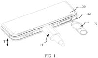
- FIG. 1 is a schematic diagram of a partial structure of a mobile phone according to some embodiments of this application.
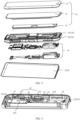
- FIG. 2 is an exploded view of the mobile phone in FIG. 1 .
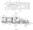
- FIG. 3 is a partial structural view of a housing 20 in FIG. 2 from another perspective.
- the mobile phone includes a housing 20, a display screen 30, and a circuit board assembly 10.
- the housing 20 includes a bottom wall 201, a side wall 202 arranged at a periphery of the bottom wall 201, and a rear cover 22 connected to the side wall 202, where the bottom wall 201, the side wall 202, and the rear cover 22 enclose an accommodating space 203, the circuit board assembly 10 is arranged in the accommodating space 203, and a socket 23 is provided on the side wall 202.
- the socket 23 includes a first socket 231 for plugging a SIM card and a second socket 232 for plugging a plug 71 of an external device.
- the display screen 30 is arranged on a side of the bottom wall 201 away from the accommodating space 203. An edge of the display screen 30 bends toward a side of the rear cover 22 and is connected to the side wall 202.
- Both a material of the bottom wall 201 and a material of the side wall 202 may be metal or a combination of metal and plastic.
- the metal part may be used as an antenna radiator 63.
- the antenna radiator 63 is configured to transmit and receive electromagnetic wave signals.
- the bottom wall 201 and the side wall 202 may be fixed by bonding or soldering. This is not specifically limited herein.
- the display screen 30 is electrically connected to the circuit board assembly 10, and is configured to display images, text, and the like.
- the display screen 30 is a flexible screen.
- the display screen 30 is an OLED (Organic Light-Emitting Diode; and organic light-emitting diode) screen.
- the display screen 30 includes a display panel 31, a protective cover plate 32, and a backplane 33.
- the display panel 31 is arranged on a side of the bottom wall 201 away from the accommodating space 203.
- the protective cover plate 32 is attached to a side of the display panel 31 away from the bottom wall 201, to protect the display panel 31.
- the protective cover plate 32 is a flexible glass plate, and an edge of the protective cover plate 32 bends toward a side of the rear cover 22 and is connected to the side wall 202.
- the backplane 33 is connected to a side of the display panel 31 close to the bottom wall 201 and is connected to the bottom wall 201, to protect the display panel 31 and dissipate heat.
- FIG. 4 is a simplified cross-sectional view of a connection between a circuit board assembly 10 and a housing 20 in the conventional technology.
- the circuit board assembly 10 in the conventional technology includes a circuit board 1 and a first component 40, a second component 45, and a third component 50 that are arranged on the circuit board 1.
- the first component 40 and the third component 50 are arranged on a side surface of the circuit board 1 close to a rear cover 22, and a height H3 of the third component 50 is greater than a height H1 of the first component 40; and the second component 45 is arranged on a side surface of the circuit board 1 away from the rear cover 22, and the second component 45 includes a card holder 451 for plugging a SIM card.
- a first socket 231 also needs to accordingly move in a direction close to the rear cover 22, to avoid a bent edge of the display screen 30. Since the card holder 451 corresponds to a position of the first socket 231 that is for plugging the SIM card and that is on a side wall 202, the circuit board 1 on which the second component 45 is arranged also needs to move as a whole in a direction close to the rear cover 22. In this way, a thickness of a mobile phone is affected by the third component 50 with a higher height on a side surface of the circuit board 1 close to the rear cover 22. The higher the height of the third component 50 is, the farther the rear cover 22 needs to be designed to be away from the bottom wall 201, and the thicker the mobile phone is, which is not beneficial to thinning and lighting of the mobile phone.
- FIG. 5 is a simplified cross-sectional view of a connection between a circuit board assembly 10 and a housing 20 according to an embodiment of this application.
- FIG. 6 is a structural diagram of a circuit board assembly 10 from one perspective according to an embodiment of this application.
- FIG. 7 is an exploded view of the circuit board assembly 10 in FIG. 6 from another perspective.
- FIG. 5 only schematically shows a simplified structural diagram of a circuit board assembly 10 and a schematic diagram of a connection of a housing 20 according to some embodiments of this application, but a structure of the circuit board assembly 10 is not limited to that shown in FIG. 5 .
- the circuit board assembly 10 includes: a first circuit board 11, a second component 45, and a second circuit board 12.
- the first circuit board 11 is located on a side of the second circuit board 12 close to a rear cover 22.
- the first circuit board 11 includes a first surface 111 and a second surface 112 that are arranged opposite to each other.
- a first component 40 is arranged on the first surface 111
- a second component 45 is arranged at a socket 23, and at least a part of the second component 45 is arranged on a side of the first circuit board 11 facing away from the first surface 111.
- a part of the second circuit board 12 is arranged on the second surface 112 in a stacking manner.
- a third component 50 is arranged on the second circuit board 12.
- a height H3 of the third component 50 is greater than a height H1 of the first component 40, and the third component 50 overlaps with the first circuit board 11 in a thickness direction T of the first circuit board 11.
- overlap specifically means that sizes of two components in a specific direction overlap with each other to a specific extent.
- that the third component 50 overlaps with the first circuit board 11 in the thickness direction T of the first circuit board 11 means: A size of the first circuit board 11 overlaps with a size of the third component 50 to a specific extent in the thickness direction T of the first circuit board 11.
- orthographic projections of the first circuit board 11 and the third component 50 on a plane perpendicular to the first circuit board 11 have overlapping regions.
- a height of the third component 50 protruding from the first circuit board 11 is reduced by a thickness of at least one first circuit board 11, so that the rear cover 22 can be designed closer to a bottom wall 201. This helps reduce a thickness of a mobile phone.
- both the first circuit board 11 and the second circuit board 12 are rigid circuit boards. In this way, additional assembly procedures and positioning structures are not needed, which facilitates assembly and connection of the circuit board assembly 10, and is beneficial to transformation of the circuit board assembly 10.
- an area for arranging components is increased, and a production cost of the rigid circuit board is lower, which is beneficial to controlling a production cost of the circuit board assembly 10.
- the first circuit board 11 is electrically connected to the second circuit board 12 through a solder material.
- the first circuit board 11 is fixedly connected to the second circuit board 12 through the solder material, and the solder material plays a structural fixing role.
- the first circuit board 11 may be electrically connected to the second circuit board 12 through the solder material, and the solder material plays a role of signal communication, so that a function of the circuit board assembly 10 is consistent with a function of arranging all components on one circuit board.
- the solder material may be in the form of dots, so that after the second circuit board 12 and the first circuit board 11 are soldered by the solder material, a distance between soldering surfaces of the first circuit board 11 and the second circuit board 12 may be effectively controlled, so that the second circuit board 12 is more attached to the second surface 112 of the first circuit board 11.
- a distance between the second circuit board 12 and the second surface 112 of the first circuit board 11 is negligible.
- a position of the solder material on the second surface 112 may be selected by a user on the premise of ensuring reliability of a connection between the first circuit board 11 and the second circuit board 12. This is not specifically limited herein.
- the first circuit board 11 and the second circuit board 12 may also be electrically connected to each other through a wire or a conductive component.
- the conductive component may be a conductive pin or a conductive elastic piece. This is not specifically limited herein.
- an avoidance opening 13 is provided on the first circuit board 11, the third component 50 is arranged at the avoidance opening 13 on the second circuit board 12, and a part (certainly, all) of the third component 50 is located at the avoidance opening 13.
- a quantity of avoidance openings 13 may be the same as a quantity of third components 50, and the avoidance openings 13 are in one-to-one correspondence with the third components 50.
- One or more third components 50 may also be arranged at one avoidance opening 13. This is not specifically limited herein.
- the avoidance opening 13 runs through the first circuit board 11 in the thickness direction T of the first circuit board 11. After the avoidance opening 13 runs through the first circuit board 11, it is convenient for the third component 50 to run through the avoidance opening 13.
- the avoidance opening 13 may also not run through the first circuit board 11, as shown in FIG. 8 . This is not specifically limited herein.
- FIG. 8 is a simplified diagram of a connection between a housing 20 and a circuit board assembly 10 according to some other embodiments of this application.
- a first circuit board 11 and a second circuit board 12 are arranged in a stacking manner through an elevated board 16.
- a component with a higher height may be arranged between the first surface 111 and the second circuit board 12, to increase an area for arranging components.
- arranging the elevated board 16 with the first circuit board 11 and the second circuit board 12 in a stacking manner stability and reliability of a connection between the first circuit board 11 and the second circuit board 12 are improved.
- a third component 50 is arranged on a side surface of the second circuit board 12 close to the first circuit board 11, and is located between the first circuit board 11 and the second circuit board 12.
- a sum of a thickness of the elevated board 16 and a thickness of the second circuit board 12 is less than a height of a second component 45.
- a part of the third component 50 is arranged higher than the first surface 111, and a distance h1 of the third component 50 higher than the first surface 111 is less than a height H1 of a first component 40.
- a distance protruding from the first surface 111 is determined by the height of the first component 40 with a lower height.
- a rear cover 22 can be designed closer to a bottom wall 201, which is beneficial to reducing a thickness of a mobile phone.
- the distance h1 of the third component 50 higher than the first surface 111 is less than the height H1 of the first component 40
- the distance h1 of the third component 50 higher than the first surface 111 may also be equal to the height H1 of the first component 40. This is not specifically limited herein.
- the second circuit board 12 includes a first region 122, the first region 122 extends beyond an edge on a side of the first circuit board 11, and the third component 50 is arranged in the first region 122.
- an area for arranging the third component 50 with a higher height on the second circuit board 12 is increased.
- the third component 50 is arranged on the first region 122, and a case of opening an avoidance opening 13 on the first circuit board 11 for the third component 50 to pass through is avoided.
- manufacturing procedures of the first circuit board 11 are reduced.
- one part of the plurality of third components 50 may be arranged on the first region 122, and the other part of third components 50 are arranged on the second circuit board 11 and protrude from the first surface 111 through the avoidance opening 13 on the first circuit board 11.
- an area for providing the avoidance opening 13 at the position of the first circuit board 11 corresponding to the third component 50 is reduced, and a strength of the first circuit board 11 is improved, thereby improving flexibility of arrangement of the third component 50 on the second circuit board 12.
- FIG. 9 is a structural diagram of the circuit board assembly 10 in FIG. 6 from another perspective.
- the second component 45 is higher than a third surface 121, where the third surface 121 is a side surface of the second circuit board 12 facing away from the first circuit board 11.
- a component with a lower height may be arranged on the third surface 121. This increases an area for arranging components, and optimizes arrangement of the components on the circuit board assembly 10.
- the second component 45 includes a card holder 451 for plugging a SIM card, and the card holder 451 is arranged on the second surface 112. In this way, arrangement of the card holder 451 makes full use of a space between the first circuit board 11 and the bottom wall 201, and avoids wasting the space between the first circuit board 11 and the bottom wall 201. This improves space utilization of an accommodating space 203.
- the card holder 451 may also be arranged on a side surface of the second circuit board 12 close to the second surface 112. This is not specifically limited herein.
- the card holder 451 is used in this way.
- the card holder 451 passes through a socket 23 provided on a side wall 202, and a pin 72 is inserted through an insertion hole 25 provided on the side wall 202, so that the card holder 451 pops out of a housing 20.
- the card holder 451 moves toward the inside of the housing 20 in a direction of the inside of the housing 20.
- the pin 72 is also used to pop the card holder 451 out of the housing 20. This is not described herein again.
- a quantity of second circuit boards 12 is two, the two second circuit boards 12 are spaced apart to form a limiting groove 14, and the card holder 451 is arranged in the limiting groove 14.
- the two second circuit boards 12 are spaced apart to form the limiting groove 14.
- the limiting groove 14 effectively limits movement of the card holder 451 in a direction perpendicular to a thickness direction T of the first circuit board 11. This avoids a case in which the card holder 451 looses in a process of frequent insertion and removal, resulting in poor contact with the first circuit board 11.
- a quantity of second circuit boards 12 may also be one, three, four, and the like.
- the limiting groove 14 is provided on the second circuit board 12 at a position corresponding to the card holder 451. In this way, a quantity of components of the circuit board assembly 10 is reduced, and overall functional consistency of the circuit board assembly 10 is improved.
- the second component 45 includes an interface unit 452 for plugging a plug 71 of the external device, the interface unit 452 is arranged on the second circuit board 12, and a part of the interface unit 452 overlaps with the first circuit board 11 and the second circuit board 12 in the thickness direction T of the first circuit board 11.
- the interface unit 452 is arranged on the second circuit board 12, and a part of the interface unit 452 overlaps with the first circuit board 11 and the second circuit board 12 in the thickness direction T of the first circuit board 11.
- a size of the interface unit 452 overlaps with a thickness of the first circuit board 11 and a thickness of the second circuit board 12 is avoided. This is beneficial to reducing an overall size of the circuit board assembly 10 in the thickness direction T of the first circuit board 11.
- the interface unit 452 may be configured to be connected to an external power supply device for charging the mobile phone.
- the interface unit 452 may be any one of a Type-C interface, a Micro-USB interface, and a Mini-USB interface. This is not specifically limited herein.
- the interface unit 452 may also be a USB interface or a headphone interface. This is not specifically limited herein.
- a part of the interface unit 452 may overlap with both the first circuit board 11 and the second circuit board 12, or may overlap with one of the first circuit board 11 or the second circuit board 12.
- FIG. 10 is an exploded view of a connection structure between a circuit board assembly 10 and a speaker 64 and an antenna board 65 according to some embodiments of this application.
- FIG. 11 is a schematic diagram of a partial structure of the circuit board assembly 10 in FIG. 6 .
- An avoidance space 15 that runs through the first circuit board 11 and the second circuit board 12 is arranged at a position of an interface unit 452.
- One part (referring to a connecting part 4521 of the interface unit 452) of the interface unit 452 is arranged on a third surface 121.
- the other part referring to a slot portion 4522 where a plug 73 of an external device is plugged into the interface unit 452) of the interface unit 452 is located in the avoidance space 15.
- the third surface 121 is a side surface of the second circuit board 12 facing away from the first circuit board 11.
- a lateral space that is of the first circuit board 11 and the second circuit board 12 and that is occupied by the interface unit 452 may be reduced. This reduces a size (such as a width) of the circuit board assembly 10 in a direction parallel to the first circuit board 11, which is beneficial to reducing occupation of the accommodating space 203 by the circuit board assembly 10.
- the avoidance space 15 may limit a position of the interface unit 452, which is beneficial to improving reliability of an electrical connection between the interface unit 452 and the second circuit board 12.
- the interface unit 452 may also be arranged on the second surface 112, toward a side of the second circuit board 12, or the interface unit 452 may be arranged on a side surface of the second circuit board 12 close to the second surface 112, toward a side of the first surface 111 or a side of the third surface 121. This is not specifically limited herein.
- a part of the interface unit 452 is higher than the first surface 111, and a distance of the interface unit 452 higher than the first surface 111 is less than the height of the first component 40.
- a distance of the interface unit 452 higher than the first surface 111 is less than a height of a second elastic piece 402.
- the interface unit 452 is still determined by a component with a highest height among the first components 40 with lower heights.
- a distance between the first surface 111 and the rear cover 22 is not additionally increased due to the interface unit 452. This improves space utilization of the circuit board assembly 10 in the accommodating space 203.
- an end of the interface unit 452 that is for plugging of the external device is fixed on the third surface 121 through a connecting ear 18.
- the connecting ear 18 concaves toward a side facing the first surface 111 and overlaps with the third surface 121, so that the end of the interface unit 452 that is for plugging of the external device is located in an avoidance space 15.
- Arrangement of the connecting ear 18 well limits movement of the interface unit 452 in a direction parallel to the first circuit board 11. This improves reliability of an electrical connection between the interface unit 452 and the second circuit board 12, and improves reliability of the circuit board assembly 10.
- first components 40 and third components 50 there are a plurality of first components 40 and third components 50, and the distance of each of the third components 50 higher than the first surface 111 is less than a maximum value of the height of the first component 40.
- each third component 50 is increased when a distance between the rear cover 22 and the first circuit board 11 is reduced.
- a plurality of first components 40 are respectively a first elastic piece 401 and a second elastic piece 402.
- the first elastic piece 401 is arranged at an edge of the first surface 111, and is configured to be electrically connected to an antenna radiator 63
- the second elastic piece 402 is configured to be electrically connected to a speaker 64.
- the antenna and the speaker 64 are electrically connected to the first circuit board 11 through the first elastic piece 401 and the second elastic piece 402 respectively.
- the speaker 64 includes a lower cover body 641, a speaker driver 643, and a second flexible circuit board 61.
- the lower cover body 641 has a cavity 642.
- the speaker driver 643 is arranged in the cavity 642.
- One end of the second flexible circuit board 61 is electrically connected to the speaker driver 643, and the other end of the second flexible circuit board 61 is electrically connected to the circuit board assembly 10 through the second elastic piece 402.
- the lower cover body 641 is fixed to the bottom wall 201, so that the speaker 64 is fixed to the housing 20.
- a space enclosed by the cavity 642 and the bottom wall 201 of the housing 20 forms a sound cavity.
- the speaker 64 is closely attached to the bottom wall 201, which saves a space of an accommodating space 203 occupied by an upper cover body, and further reduces a thickness of the mobile phone.
- a sound output hole 24 is provided on the side wall 202 of the housing 20 corresponding to a sound output portion of the sound cavity of the speaker 64.
- the sound output hole 24 is configured to release sound emitted by the speaker driver 643 out of the housing 20.
- a dust-proof net 644 is arranged between the sound output hole 24 and the sound output portion of the sound cavity. By arranging the dust-proof net 644, metal particles and other dust are prevented from entering the speaker 64 through the sound output hole 24, to reduce an impact of dust on performance of the speaker 64.
- a quantity of sound output holes 24 needs to be determined based on factors such as a size of the side wall 202 of the housing 20, and arrangement of the speaker driver 643 and the sound cavity. This is not specifically limited herein.
- FIG. 12 is a cross-sectional view of A-A in FIG. 6 .
- a plurality of third components 50 are a microphone component 501, a connector assembly 504, and an antenna connector assembly 508 respectively.
- the microphone component 501 includes a microphone 502 and a shielding case 503.
- the shielding case 503 is arranged on the second circuit board 12, and the microphone 502 is arranged in the shielding case 503.
- an avoidance opening 13 running through the first circuit board 11 is provided on a side of the first circuit board 11, and the microphone component 501 is located in the avoidance opening 13 as a whole.
- a height of the microphone component 501 is a height of the shielding case 503.
- the height of the microphone component 501 is a distance between the side surface of the second circuit board 12 close to the second surface 112 and a highest point of an outer bottom wall 201 of the shielding case 503.
- the height of the microphone component 501 is greater than a height of the first elastic piece 401
- the microphone component 501 is higher than the first surface 111
- the height of the microphone component 501 higher than the first surface 111 is less than the height of the first component 40 such as the first elastic piece 401.
- the connector assembly 504 includes a fixing member 505, a first connector 506 arranged on the second circuit board 12, and a second connector 507 configured to be connected to the first flexible circuit board 60.
- the second connector 507 is electrically connected to the first connector 506, and the fixing member 505 is configured to relatively fix the second connector 507 and the first connector 506.
- the second connector 507 and the first connector 506 are located in the avoidance opening 13.
- a structure of the fixing member 505 is in a plate shape.
- the first connector 506 and the second connector 507 may be male and female sockets of a BTB connector.
- the first connector 506 is connected to the second connector 507 through the fixing member 505, so that the circuit board assembly 10 is electrically connected to a main board.
- a height of the connector assembly 504 includes a distance between a highest point of a side surface of the fixing member 505 away from the second circuit board 12 and a side surface of the second circuit board 12 on which the second connector 507 is located.
- FIG. 7 there are two first flexible circuit boards 60 and two connector assemblies 504. Because a distance between the two connector assemblies 504 is close, to reduce a quantity of components of the circuit board assembly 10, fixing members 505 in the two connector assemblies 504 are processed into an integrated plate-shaped structure. In this way, the fixing member 505 lays the first flexible circuit board 60 on the first surface 111 of the first circuit board 11, to avoid damage to the first flexible circuit board 60 in an assembly process of the circuit board assembly 10. This improves reliability of an electrical connection between the first flexible circuit board 60 and the circuit board assembly 10.
- two fixing members 505 may also be correspondingly arranged. This is not specifically limited herein.
- an antenna connector assembly 508 includes a connector body 5081 and a pressing plate 5082 that are arranged on the second circuit board 12.
- the connector body 5081 is arranged on a first region 122 of the second circuit board 12.
- One end of the third flexible circuit board 62 is electrically connected to the antenna connector assembly 508 through the pressing plate 5082.
- the other end of the third flexible circuit board 62 is electrically connected to an antenna board 65, so that the antenna board 65 is electrically connected to the circuit board assembly 10.
- the pressing plate 5082 and the lower cover body 641 of the speaker 64 are an integral structure. This setting reduces a quantity of components of the mobile phone.
- the third flexible circuit board 62 may be electrically connected to the circuit board assembly 10 in a manner of bending, folding, and the like, so that the third flexible circuit board 62 matches an internal space of the accommodating space 203, has better flexibility, and takes up less space than a hard circuit board. This saves an ultrasonic soldering procedure, and further reduces an assembly cost of the circuit board assembly 10.
- a quantity of antenna boards 65 may be one or more, to increase feed points of an antenna, and improve a signal strength of the antenna.
- a specific quantity and position of the antenna board 65 are selected based on actual needs. This is not specifically limited herein.
- a fourth component 55 is arranged on the third surface 121, and a height of the fourth component 55 is less than a maximum value of a distance of the second component 45 higher than the third surface 121.
- a thickness of the circuit board assembly 10 namely, a size of the circuit board assembly 10 in a thickness direction T of the first circuit board 11
- An impact of the fourth component 55 on a thickness of the circuit board assembly 10 is reduced, and an excessive thickness of the circuit board assembly 10 is avoided. This enables arrangement in the accommodating space 203 to be more compact.
- the fourth component 55 includes a conductive elastic piece 551, the conductive elastic piece 551 is connected to a connecting member 552, and a part of the connecting member 552 extends beyond an edge of the third surface 121 and extends toward a side of the first circuit board 11, to be electrically connected to an antenna radiator 63.
- the connecting member 522 is arranged. This helps the conductive elastic piece 551 to be electrically connected to the antenna radiator 63 on a side surface of the circuit board assembly 10. Then, there is no need to provide fixing holes at positions of the first circuit board 11 and the second circuit board 12 on which the conductive elastic piece 551 is located for the conductive elastic piece 551 (which is similar to a mounting structure of the first elastic piece 401 in FIG. 6 ) to be mounted. This avoids a case in which the fixing holes occupy a space on the first circuit board 11 and the second circuit board 12.
- the conductive elastic piece 551 and the connecting member 552 may be integrally formed, or may be separate structures connected by soldering or conductive bonding. This is not specifically limited herein.
- each conductive elastic piece 551 is connected to one connecting member 552, and is electrically connected to one antenna radiator 63.
- a plurality of antenna radiators 63 are arranged on the side wall 202 and are spaced apart in a circumferential direction of the bottom wall 201.
- Each connecting member 552 is electrically connected to one antenna radiator 63, to form a feed point of an antenna. Arrangement of the plurality of antenna radiators 63 increases feed points of the antenna, and improves a signal strength of the antenna.
- the fourth component 55 further includes a conductive member 553, and the conductive member 553 is electrically connected to a metal part of the bottom wall 201.
- a mounting hole 17 is provided on the second circuit board 12, and the conductive member 553 is arranged on a periphery of the mounting hole 17. After a fastener passes through the mounting hole 17 to connect the circuit board assembly 10 to the bottom wall 201, the conductive member 553 is electrically connected to the metal part of the bottom wall 201.
- the foregoing fastener may be a screw or a bolt. This is not specifically limited herein.
- the conductive member 553 may be configured for feeding or grounding of the antenna.
- the conductive member 553 may be a large elastic piece.
- a quantity of conductive members 553 may be one, and the conductive member 553 is arranged at one mounting hole 17; and a quantity of conductive members 553 may also be more than one.
- one conductive member 553 is arranged at each mounting hole 17, to improve reliability of an electrical connection between the circuit board assembly 10 and the bottom wall 201.
- the conductive member 553 may also be a metal spring, or the like. This is not specifically limited herein.
Landscapes
- Engineering & Computer Science (AREA)
- Microelectronics & Electronic Packaging (AREA)
- Signal Processing (AREA)
- Telephone Set Structure (AREA)
- Combinations Of Printed Boards (AREA)
- Mounting Of Printed Circuit Boards And The Like (AREA)
Abstract
Description
- This application claims priority to
Chinese Patent Application No. 202221722187.2, filed with the China National Intellectual Property Administration on July 4, 2022 - This application relates to the field of electrical devices, and in particular, to a circuit board assembly and an electronic device.
- With the development of electronic technologies, for an electronic device such as a mobile phone, to achieve a more extreme appearance effect, bend processing is performed on an edge of a display screen. How to reduce a thickness of the electronic device when the edge of the display screen bends has become an important issue in the industry.
- The electronic device in the conventional technology often has a card holder for inserting a SIM card or a component for plugging a plug of an external device. A socket corresponding to the card holder or component is provided on a housing of the electronic device. When the edge of the display screen bends in a direction close to a rear cover, the socket also needs to accordingly move in a direction close to the rear cover, to avoid the bent edge of the display screen. Components such as the card holder need to correspond to a position of the socket on the housing, and therefore, a circuit board on which the components such as the card holder are arranged also needs to move in the direction of the rear cover as a whole, and electronic components on the circuit board also accordingly move as a whole. In this way, the thickness of the electronic device is affected by a component with a higher height on a side surface of the circuit board close to the rear cover. The higher the height of the component, the greater the thickness of the electronic device. This is not beneficial to thinning and lighting of the electronic device.
- Embodiments of this application provide a circuit board assembly and an electronic device, to resolve a problem in the conventional technology that a thickness of the entire electronic device is large.
- To achieve the foregoing objective, the following technical solutions are used in embodiments of this application.
- According to a first aspect, an embodiment of this application provides a circuit board assembly. The circuit board assembly includes a first circuit board, a second component, and a third circuit board. The first circuit board includes a first surface and a second surface that are arranged opposite to each other, where a first component is arranged on the first surface; and at least a part of the second component is arranged on a side of the first circuit board facing away from the first surface, and the second component is configured for plugging at least one of a SIM card and a plug of an external device; and the second circuit board is at least partially arranged on the second surface in a stacking manner, a third component is arranged on the second circuit board, a height of the third component is greater than a height of the first component, and the third component at least partially overlaps with the first circuit board in a thickness direction of the first circuit board.
- By using the foregoing solution, in the thickness direction of the first circuit board, the height of the third component protruding from the first circuit board is reduced by a thickness of at least one first circuit board, so that the rear cover can be designed closer to the bottom wall. This helps reduce a thickness of a mobile phone.
- In some embodiments, an avoidance opening is provided on the first circuit board, the third component is arranged at the avoidance opening on the second circuit board, and the third component is at least partially located in the avoidance opening.
- Compared with arranging the third component outside an edge on a side of the second circuit board on the first circuit board, the foregoing solution reduces an area of the second circuit board located outside the edge on the side of the first circuit board. This further reduces a size (such as a width) of the circuit board assembly in a direction parallel to the first circuit board, which is beneficial to reducing occupation of an accommodating space by the circuit board assembly.
- In some embodiments, the avoidance opening runs through the first circuit board in the thickness direction of the first circuit board.
- By using the foregoing solution, after the avoidance opening runs through the first circuit board, it is convenient for the third component to run through the avoidance opening.
- In some embodiments, the second circuit board includes a first region, the first region extends beyond an edge on a side of the first circuit board, and the third component is arranged in the first region.
- By using the foregoing solution, an area for arranging the higher third component on the second circuit board is increased. When there are a plurality of third components, an area for providing an avoidance opening at a position of the first circuit board corresponding to the third component is reduced, and a strength of the first circuit board is improved. When there is one third component, an avoidance opening for the third component to pass through is not provided on the first circuit board. When the thickness of the mobile phone is not affected, manufacturing procedures of the first circuit board are reduced. This further improves flexibility of arranging the third component on the second circuit board.
- In some embodiments, a part of the third component is arranged higher than the first surface, and a distance of the third component higher than the first surface is less than the height of the first component.
- By using the foregoing solution, the distance protruding from the first surface is determined by the height of the first component that is less than the height of the third component. This is beneficial to reducing a thickness of the entire electronic device.
- In some embodiments, there are a plurality of first components and third components, and the distance of each of the third components higher than the first surface is less than a maximum value of the height of the first component.
- By using the foregoing solution, a height range of each third component is increased when a distance between the rear cover and the first circuit board is reduced.
- In some embodiments, the second component includes a card holder for plugging the SIM card, and the card holder is arranged on the second surface.
- By using the foregoing solution, a space between the first circuit board and the bottom wall may be fully utilized. This further improves space utilization of the accommodating space.
- In some embodiments, a quantity of second circuit boards is two, and the two second circuit boards are spaced apart to form a limiting groove, and the card holder is arranged in the limiting groove.
- By using the foregoing solution, the limiting groove effectively limits movement of the card holder in a direction parallel to the first circuit board. This avoids a case in which the card holder looses in a process of frequent insertion and removal, resulting in poor contact with the first circuit board.
- In some embodiments, the second component includes an interface unit for plugging the plug of the external device, the interface unit is arranged on the second circuit board, and a part of the interface unit overlaps with at least one of the first circuit board and the second circuit board in the thickness direction of the first circuit board.
- By using the foregoing solution, a case in which a size of the interface unit overlaps with a thickness of the first circuit board and a thickness of the second circuit board is avoided. This is beneficial to reducing an overall size of the circuit board assembly in the thickness direction of the first circuit board.
- In some embodiments, a part of the interface unit is higher than the first surface, and a distance of the interface unit higher than the first surface is less than the height of the first component.
- By using the foregoing solution, a distance between the first surface and the rear cover is not additionally increased due to the interface unit in the thickness direction of the first circuit board. This improves space utilization of the circuit board assembly in the accommodating space.
- In some embodiments, an avoidance space running through the first circuit board and the second circuit board is arranged at a position of the interface unit, one part of the interface unit is arranged on a side surface of the second circuit board facing away from the first circuit board, and the other part of the interface unit is located in the avoidance space.
- By using the foregoing solution, a lateral space that is of the first circuit board and the second circuit board and that is occupied by the interface unit may be reduced. This reduces a size (such as a width) of the circuit board assembly in a direction parallel to the first circuit board, which is beneficial to reducing occupation of the accommodating space by the circuit board assembly. In addition, the avoidance space may limit a position of the interface unit, which is beneficial to improving reliability of an electrical connection between the interface unit and the second circuit board.
- In some embodiments, the second component is at least partially higher than a third surface, and the third surface is the side surface of the second circuit board facing away from the first circuit board.
- By using the foregoing solution, a component with a lower height may be arranged on the third surface. This increases an arrangement area of the component, and optimizes arrangement of the component on the circuit board assembly.
- In some embodiments, a fourth component is arranged on the third surface, and a height of the fourth component is less than a maximum value of a distance of the second component higher than the third surface.
- By using the foregoing solution, an impact of the fourth component on a thickness of the circuit board assembly is reduced, and an excessive thickness of the circuit board assembly is avoided. This enables arrangement in the accommodating space to be more compact.
- In some embodiments, the fourth component includes a conductive elastic piece, the conductive elastic piece is connected to a connecting member, and a part of the connecting member extends beyond an edge of the third surface and extends toward a side of the first circuit board, to be electrically connected to an antenna radiator.
- By using the foregoing solution, this helps the conductive elastic piece to be electrically connected to the antenna radiator on a side surface of the circuit board assembly. Then, there is no need to provide fixing holes at positions of the first circuit board and the second circuit board on which the conductive elastic piece is located for the conductive elastic piece to be mounted. This avoids a case in which the fixing holes occupy a space on the first circuit board and the second circuit board.
- In some embodiments, both the first circuit board and the second circuit board are rigid circuit boards; and/or the first circuit board is electrically connected to the second circuit board through solder joints.
- By using the foregoing solution, additional assembly procedures and positioning structures are not needed, which facilitates assembly and connection of the circuit board assembly, and is beneficial to transformation of the circuit board assembly. In addition, compared with a combination of a rigid circuit and a flexible circuit board, the foregoing solution is beneficial to control a production cost of the circuit board assembly.
- According to a second aspect, embodiments of this application provide an electronic device, including a housing, a display screen, and the circuit board assembly according to the first aspect. The housing includes a bottom wall, a side wall arranged at a periphery of the bottom wall, and a rear cover connected to the side wall, where the bottom wall, the side wall, and the rear cover enclose an accommodating space, and a socket that is available to be inserted by a SIM card and a plug of an external device is provided on the side wall; the display screen is arranged on a side of the bottom wall away from the accommodating space, where an edge of the display screen bends toward a side of the rear cover and is connected to the side wall; and the circuit board assembly is arranged in the accommodating space, where the first circuit board is located on a side of the second circuit board close to the rear cover, and the second component is arranged at the socket.
- Beneficial effects of the electronic device in embodiments of this application are the same as beneficial effects of the circuit board assembly in the first aspect. This is not described herein again.
-
-
FIG. 1 is a schematic diagram of a partial structure of a mobile phone according to some embodiments of this application; -
FIG. 2 is an exploded view of the mobile phone inFIG. 1 ; -
FIG. 3 is a structural diagram of a housing inFIG. 2 from one perspective; -
FIG. 4 is a simplified cross-sectional view of a connection between a circuit board assembly and a housing in the conventional technology; -
FIG. 5 is a simplified cross-sectional view of a connection between a circuit board assembly and a housing according to an embodiment of this application; -
FIG. 6 is a structural diagram of a circuit board assembly from one perspective according to an embodiment of this application; -
FIG. 7 is an exploded view of the circuit board assembly inFIG. 6 from another perspective; -
FIG. 8 is a simplified diagram of a connection between a housing and a circuit board assembly according to some other embodiments of this application; -
FIG. 9 is a structural diagram of the circuit board assembly inFIG. 6 from another perspective; -
FIG. 10 is an exploded view of a connection structure between a circuit board assembly and a speaker and an antenna board according to some embodiments of this application; -
FIG. 11 is a schematic diagram of a partial structure of the circuit board assembly inFIG. 6 ; and -
FIG. 12 is a cross-sectional view of A-A inFIG. 6 . - In embodiments of this application, terms "first" and "second" are used merely for the purpose of description, and shall not be construed as indicating or implying relative importance or implying a quantity of indicated technical features. Therefore, a feature limited by "first" or "second" may explicitly or implicitly include one or more features.
- In embodiments of this application, it should be noted that, a term "electrical connection" should be understood in a broad sense. For example, current conduction may be implemented in a manner of direct connection, or conduction of electrical energy may be implemented in a manner of capacitive coupling.
- An electronic device in embodiments of this application may be an electronic device into which a SIM card needs to be inserted or an electronic device that includes a component for plugging a plug of an external device such as a mobile phone, a tablet computer, an e-reader, a wearable device, a remote control, a POS (point of sales terminal; and point of sales information management system) machine, a notebook computer, a personal digital assistant (personal digital assistant, PDA), or a vehiclemounted device.
- The following describes the electronic device in embodiments of this application in detail by using the mobile phone as an example. Other types of electronic devices may be specifically configured with reference to a design concept of a
circuit board assembly 10 in a mobile phone embodiment. Details are not described herein again. -
FIG. 1 is a schematic diagram of a partial structure of a mobile phone according to some embodiments of this application.FIG. 2 is an exploded view of the mobile phone inFIG. 1 .FIG. 3 is a partial structural view of a housing 20 inFIG. 2 from another perspective. The mobile phone includes a housing 20, adisplay screen 30, and acircuit board assembly 10. - As shown in
FIG. 2 and FIG. 3 , the housing 20 includes abottom wall 201, a side wall 202 arranged at a periphery of thebottom wall 201, and arear cover 22 connected to the side wall 202, where thebottom wall 201, the side wall 202, and therear cover 22 enclose anaccommodating space 203, thecircuit board assembly 10 is arranged in theaccommodating space 203, and asocket 23 is provided on the side wall 202. For example, thesocket 23 includes afirst socket 231 for plugging a SIM card and asecond socket 232 for plugging aplug 71 of an external device. Thedisplay screen 30 is arranged on a side of thebottom wall 201 away from theaccommodating space 203. An edge of thedisplay screen 30 bends toward a side of therear cover 22 and is connected to the side wall 202. - Both a material of the
bottom wall 201 and a material of the side wall 202 may be metal or a combination of metal and plastic. The metal part may be used as anantenna radiator 63. Theantenna radiator 63 is configured to transmit and receive electromagnetic wave signals. Thebottom wall 201 and the side wall 202 may be fixed by bonding or soldering. This is not specifically limited herein. - The
display screen 30 is electrically connected to thecircuit board assembly 10, and is configured to display images, text, and the like. Thedisplay screen 30 is a flexible screen. For example, thedisplay screen 30 is an OLED (Organic Light-Emitting Diode; and organic light-emitting diode) screen. Thedisplay screen 30 includes adisplay panel 31, aprotective cover plate 32, and abackplane 33. Thedisplay panel 31 is arranged on a side of thebottom wall 201 away from theaccommodating space 203. Theprotective cover plate 32 is attached to a side of thedisplay panel 31 away from thebottom wall 201, to protect thedisplay panel 31. Theprotective cover plate 32 is a flexible glass plate, and an edge of theprotective cover plate 32 bends toward a side of therear cover 22 and is connected to the side wall 202. Thebackplane 33 is connected to a side of thedisplay panel 31 close to thebottom wall 201 and is connected to thebottom wall 201, to protect thedisplay panel 31 and dissipate heat. -
FIG. 4 is a simplified cross-sectional view of a connection between acircuit board assembly 10 and a housing 20 in the conventional technology. Thecircuit board assembly 10 in the conventional technology includes acircuit board 1 and afirst component 40, asecond component 45, and athird component 50 that are arranged on thecircuit board 1. Thefirst component 40 and thethird component 50 are arranged on a side surface of thecircuit board 1 close to arear cover 22, and a height H3 of thethird component 50 is greater than a height H1 of thefirst component 40; and thesecond component 45 is arranged on a side surface of thecircuit board 1 away from therear cover 22, and thesecond component 45 includes acard holder 451 for plugging a SIM card. - When an edge of a
display screen 30 bends in a direction close to therear cover 22, afirst socket 231 also needs to accordingly move in a direction close to therear cover 22, to avoid a bent edge of thedisplay screen 30. Since thecard holder 451 corresponds to a position of thefirst socket 231 that is for plugging the SIM card and that is on a side wall 202, thecircuit board 1 on which thesecond component 45 is arranged also needs to move as a whole in a direction close to therear cover 22. In this way, a thickness of a mobile phone is affected by thethird component 50 with a higher height on a side surface of thecircuit board 1 close to therear cover 22. The higher the height of thethird component 50 is, the farther therear cover 22 needs to be designed to be away from thebottom wall 201, and the thicker the mobile phone is, which is not beneficial to thinning and lighting of the mobile phone. -
FIG. 5 is a simplified cross-sectional view of a connection between acircuit board assembly 10 and a housing 20 according to an embodiment of this application.FIG. 6 is a structural diagram of acircuit board assembly 10 from one perspective according to an embodiment of this application.FIG. 7 is an exploded view of thecircuit board assembly 10 inFIG. 6 from another perspective. It should be noted that,FIG. 5 only schematically shows a simplified structural diagram of acircuit board assembly 10 and a schematic diagram of a connection of a housing 20 according to some embodiments of this application, but a structure of thecircuit board assembly 10 is not limited to that shown inFIG. 5 . Thecircuit board assembly 10 includes: afirst circuit board 11, asecond component 45, and asecond circuit board 12. Thefirst circuit board 11 is located on a side of thesecond circuit board 12 close to arear cover 22. - The
first circuit board 11 includes afirst surface 111 and asecond surface 112 that are arranged opposite to each other. Afirst component 40 is arranged on thefirst surface 111, asecond component 45 is arranged at asocket 23, and at least a part of thesecond component 45 is arranged on a side of thefirst circuit board 11 facing away from thefirst surface 111. A part of thesecond circuit board 12 is arranged on thesecond surface 112 in a stacking manner. Athird component 50 is arranged on thesecond circuit board 12. A height H3 of thethird component 50 is greater than a height H1 of thefirst component 40, and thethird component 50 overlaps with thefirst circuit board 11 in a thickness direction T of thefirst circuit board 11. - In embodiments of this application, "overlap" specifically means that sizes of two components in a specific direction overlap with each other to a specific extent. For example, that the
third component 50 overlaps with thefirst circuit board 11 in the thickness direction T of thefirst circuit board 11 means: A size of thefirst circuit board 11 overlaps with a size of thethird component 50 to a specific extent in the thickness direction T of thefirst circuit board 11. In other words, orthographic projections of thefirst circuit board 11 and thethird component 50 on a plane perpendicular to thefirst circuit board 11 have overlapping regions. - By using the foregoing technical solution, in the thickness direction T of the
first circuit board 11, a height of thethird component 50 protruding from thefirst circuit board 11 is reduced by a thickness of at least onefirst circuit board 11, so that therear cover 22 can be designed closer to abottom wall 201. This helps reduce a thickness of a mobile phone. - In some embodiments, as shown in
FIG. 5 andFIG. 6 , both thefirst circuit board 11 and thesecond circuit board 12 are rigid circuit boards. In this way, additional assembly procedures and positioning structures are not needed, which facilitates assembly and connection of thecircuit board assembly 10, and is beneficial to transformation of thecircuit board assembly 10. In addition, in comparison to a combination of thefirst circuit board 11 being a rigid circuit board and thesecond circuit board 12 being a flexible circuit board, an area for arranging components is increased, and a production cost of the rigid circuit board is lower, which is beneficial to controlling a production cost of thecircuit board assembly 10. - In some embodiments, as shown in
FIG. 6 , thefirst circuit board 11 is electrically connected to thesecond circuit board 12 through a solder material. In this way, thefirst circuit board 11 is fixedly connected to thesecond circuit board 12 through the solder material, and the solder material plays a structural fixing role. In addition, thefirst circuit board 11 may be electrically connected to thesecond circuit board 12 through the solder material, and the solder material plays a role of signal communication, so that a function of thecircuit board assembly 10 is consistent with a function of arranging all components on one circuit board. - The solder material may be in the form of dots, so that after the
second circuit board 12 and thefirst circuit board 11 are soldered by the solder material, a distance between soldering surfaces of thefirst circuit board 11 and thesecond circuit board 12 may be effectively controlled, so that thesecond circuit board 12 is more attached to thesecond surface 112 of thefirst circuit board 11. In other words, in the thickness direction T of thefirst circuit board 11, a distance between thesecond circuit board 12 and thesecond surface 112 of thefirst circuit board 11 is negligible. A position of the solder material on thesecond surface 112 may be selected by a user on the premise of ensuring reliability of a connection between thefirst circuit board 11 and thesecond circuit board 12. This is not specifically limited herein. - Certainly, in addition to being electrically connected to each other through the solder material, the
first circuit board 11 and thesecond circuit board 12 may also be electrically connected to each other through a wire or a conductive component. The conductive component may be a conductive pin or a conductive elastic piece. This is not specifically limited herein. - In some embodiments, as shown in
FIG. 5 to FIG. 7 , anavoidance opening 13 is provided on thefirst circuit board 11, thethird component 50 is arranged at theavoidance opening 13 on thesecond circuit board 12, and a part (certainly, all) of thethird component 50 is located at theavoidance opening 13. Compared with arranging thethird component 50 outside an edge on a side of thesecond circuit board 12 on thefirst circuit board 11, this reduces an area of thesecond circuit board 12 located outside the edge on the side of thefirst circuit board 11. This further reduces a size (such as a width) of thecircuit board assembly 10 in a direction parallel to thefirst circuit board 11, which is beneficial to reducing occupation of anaccommodating space 203 by thecircuit board assembly 10. - In addition, a quantity of
avoidance openings 13 may be the same as a quantity ofthird components 50, and theavoidance openings 13 are in one-to-one correspondence with thethird components 50. One or morethird components 50 may also be arranged at oneavoidance opening 13. This is not specifically limited herein. - In some embodiments, as shown in
FIG. 7 , the avoidance opening 13 runs through thefirst circuit board 11 in the thickness direction T of thefirst circuit board 11. After the avoidance opening 13 runs through thefirst circuit board 11, it is convenient for thethird component 50 to run through theavoidance opening 13. - Certainly, in addition to running through the
first circuit board 11, theavoidance opening 13 may also not run through thefirst circuit board 11, as shown inFIG. 8 . This is not specifically limited herein. - In some embodiments,
FIG. 8 is a simplified diagram of a connection between a housing 20 and acircuit board assembly 10 according to some other embodiments of this application. Afirst circuit board 11 and asecond circuit board 12 are arranged in a stacking manner through anelevated board 16. - By arranging the
elevated board 16, a component with a higher height may be arranged between thefirst surface 111 and thesecond circuit board 12, to increase an area for arranging components. In addition, by arranging theelevated board 16 with thefirst circuit board 11 and thesecond circuit board 12 in a stacking manner, stability and reliability of a connection between thefirst circuit board 11 and thesecond circuit board 12 are improved. - In some embodiments, as shown in
FIG. 8 , in a thickness direction T of thefirst circuit board 11, athird component 50 is arranged on a side surface of thesecond circuit board 12 close to thefirst circuit board 11, and is located between thefirst circuit board 11 and thesecond circuit board 12. A sum of a thickness of theelevated board 16 and a thickness of thesecond circuit board 12 is less than a height of asecond component 45. In this way, in the thickness direction T of thefirst circuit board 11, when a size (such as a width) of thecircuit board assembly 10 in a direction parallel to thefirst circuit board 11 is reduced, through elevation of theelevated board 16, an area for arranging thethird component 50 with a higher height on the two opposite surfaces of thesecond circuit board 12 is increased. - In some embodiments, as shown in
FIG. 5 andFIG. 6 , a part of thethird component 50 is arranged higher than thefirst surface 111, and a distance h1 of thethird component 50 higher than thefirst surface 111 is less than a height H1 of afirst component 40. In this way, a distance protruding from thefirst surface 111 is determined by the height of thefirst component 40 with a lower height. In this way, arear cover 22 can be designed closer to abottom wall 201, which is beneficial to reducing a thickness of a mobile phone. - Certainly, in addition to a case in which the distance h1 of the
third component 50 higher than thefirst surface 111 is less than the height H1 of thefirst component 40, the distance h1 of thethird component 50 higher than thefirst surface 111 may also be equal to the height H1 of thefirst component 40. This is not specifically limited herein. - In some embodiments, as shown in
FIG. 6 , thesecond circuit board 12 includes afirst region 122, thefirst region 122 extends beyond an edge on a side of thefirst circuit board 11, and thethird component 50 is arranged in thefirst region 122. - By using the foregoing technical solution, an area for arranging the
third component 50 with a higher height on thesecond circuit board 12 is increased. When there is onethird component 50, thethird component 50 is arranged on thefirst region 122, and a case of opening anavoidance opening 13 on thefirst circuit board 11 for thethird component 50 to pass through is avoided. When the thickness of the mobile phone is not affected, manufacturing procedures of thefirst circuit board 11 are reduced. When there are a plurality ofthird components 50, one part of the plurality ofthird components 50 may be arranged on thefirst region 122, and the other part ofthird components 50 are arranged on thesecond circuit board 11 and protrude from thefirst surface 111 through theavoidance opening 13 on thefirst circuit board 11. In comparison to a case in which the plurality ofthird components 50 pass through thefirst circuit board 11 through theavoidance opening 13, an area for providing theavoidance opening 13 at the position of thefirst circuit board 11 corresponding to thethird component 50 is reduced, and a strength of thefirst circuit board 11 is improved, thereby improving flexibility of arrangement of thethird component 50 on thesecond circuit board 12. - As shown in
FIG. 7 andFIG. 9, FIG. 9 is a structural diagram of thecircuit board assembly 10 inFIG. 6 from another perspective. Thesecond component 45 is higher than athird surface 121, where thethird surface 121 is a side surface of thesecond circuit board 12 facing away from thefirst circuit board 11. - In this way, without increasing a thickness of the
circuit board assembly 10, a component with a lower height may be arranged on thethird surface 121. This increases an area for arranging components, and optimizes arrangement of the components on thecircuit board assembly 10. - In some embodiments, as shown in
FIG. 6 andFIG. 9 , thesecond component 45 includes acard holder 451 for plugging a SIM card, and thecard holder 451 is arranged on thesecond surface 112. In this way, arrangement of thecard holder 451 makes full use of a space between thefirst circuit board 11 and thebottom wall 201, and avoids wasting the space between thefirst circuit board 11 and thebottom wall 201. This improves space utilization of anaccommodating space 203. - Certainly, in addition to being arranged on the
second surface 112, thecard holder 451 may also be arranged on a side surface of thesecond circuit board 12 close to thesecond surface 112. This is not specifically limited herein. - The
card holder 451 is used in this way. Thecard holder 451 passes through asocket 23 provided on a side wall 202, and apin 72 is inserted through aninsertion hole 25 provided on the side wall 202, so that thecard holder 451 pops out of a housing 20. After the SIM card is placed into thecard holder 451, thecard holder 451 moves toward the inside of the housing 20 in a direction of the inside of the housing 20. When the SIM card needs to be taken out, thepin 72 is also used to pop thecard holder 451 out of the housing 20. This is not described herein again. - In some embodiments, as shown in
FIG. 5 andFIG. 9 , a quantity ofsecond circuit boards 12 is two, the twosecond circuit boards 12 are spaced apart to form a limitinggroove 14, and thecard holder 451 is arranged in the limitinggroove 14. The twosecond circuit boards 12 are spaced apart to form the limitinggroove 14. When stability and reliability of a connection between thefirst circuit board 11 and thesecond circuit board 12 are improved, the limitinggroove 14 effectively limits movement of thecard holder 451 in a direction perpendicular to a thickness direction T of thefirst circuit board 11. This avoids a case in which thecard holder 451 looses in a process of frequent insertion and removal, resulting in poor contact with thefirst circuit board 11. - In addition to a case in which a quantity of
second circuit boards 12 is two, a quantity ofsecond circuit boards 12 may also be one, three, four, and the like. For example, there is onesecond circuit board 12, and the limitinggroove 14 is provided on thesecond circuit board 12 at a position corresponding to thecard holder 451. In this way, a quantity of components of thecircuit board assembly 10 is reduced, and overall functional consistency of thecircuit board assembly 10 is improved. - In some embodiments, as shown in
FIG. 6 andFIG. 9 , thesecond component 45 includes an interface unit 452 for plugging aplug 71 of the external device, the interface unit 452 is arranged on thesecond circuit board 12, and a part of the interface unit 452 overlaps with thefirst circuit board 11 and thesecond circuit board 12 in the thickness direction T of thefirst circuit board 11. In this design, a case in which a size of the interface unit 452 overlaps with a thickness of thefirst circuit board 11 and a thickness of thesecond circuit board 12 is avoided. This is beneficial to reducing an overall size of thecircuit board assembly 10 in the thickness direction T of thefirst circuit board 11. - The interface unit 452 may be configured to be connected to an external power supply device for charging the mobile phone. The interface unit 452 may be any one of a Type-C interface, a Micro-USB interface, and a Mini-USB interface. This is not specifically limited herein. Certainly, in addition to being configured to be connected to the external power supply device for charging the mobile phone, the interface unit 452 may also be a USB interface or a headphone interface. This is not specifically limited herein.
- It should be noted that, a part of the interface unit 452 may overlap with both the
first circuit board 11 and thesecond circuit board 12, or may overlap with one of thefirst circuit board 11 or thesecond circuit board 12. -
FIG. 10 is an exploded view of a connection structure between acircuit board assembly 10 and aspeaker 64 and anantenna board 65 according to some embodiments of this application.FIG. 11 is a schematic diagram of a partial structure of thecircuit board assembly 10 inFIG. 6 . Anavoidance space 15 that runs through thefirst circuit board 11 and thesecond circuit board 12 is arranged at a position of an interface unit 452. One part (referring to a connecting part 4521 of the interface unit 452) of the interface unit 452 is arranged on athird surface 121. The other part (referring to a slot portion 4522 where a plug 73 of an external device is plugged into the interface unit 452) of the interface unit 452 is located in theavoidance space 15. Thethird surface 121 is a side surface of thesecond circuit board 12 facing away from thefirst circuit board 11. - By arranging a part of the interface unit 452 in the
avoidance space 15, a lateral space that is of thefirst circuit board 11 and thesecond circuit board 12 and that is occupied by the interface unit 452 may be reduced. This reduces a size (such as a width) of thecircuit board assembly 10 in a direction parallel to thefirst circuit board 11, which is beneficial to reducing occupation of theaccommodating space 203 by thecircuit board assembly 10. In addition, theavoidance space 15 may limit a position of the interface unit 452, which is beneficial to improving reliability of an electrical connection between the interface unit 452 and thesecond circuit board 12. - Certainly, the interface unit 452 may also be arranged on the
second surface 112, toward a side of thesecond circuit board 12, or the interface unit 452 may be arranged on a side surface of thesecond circuit board 12 close to thesecond surface 112, toward a side of thefirst surface 111 or a side of thethird surface 121. This is not specifically limited herein. - In some embodiments, as shown in
FIG. 6 , a part of the interface unit 452 is higher than thefirst surface 111, and a distance of the interface unit 452 higher than thefirst surface 111 is less than the height of thefirst component 40. For example, a distance of the interface unit 452 higher than thefirst surface 111 is less than a height of a second elastic piece 402. In this way, in a thickness direction T of thefirst circuit board 11, the interface unit 452 is still determined by a component with a highest height among thefirst components 40 with lower heights. A distance between thefirst surface 111 and therear cover 22 is not additionally increased due to the interface unit 452. This improves space utilization of thecircuit board assembly 10 in theaccommodating space 203. - In some embodiments, as shown in
FIG. 9 andFIG. 10 , an end of the interface unit 452 that is for plugging of the external device is fixed on thethird surface 121 through a connectingear 18. The connectingear 18 concaves toward a side facing thefirst surface 111 and overlaps with thethird surface 121, so that the end of the interface unit 452 that is for plugging of the external device is located in anavoidance space 15. Arrangement of the connectingear 18 well limits movement of the interface unit 452 in a direction parallel to thefirst circuit board 11. This improves reliability of an electrical connection between the interface unit 452 and thesecond circuit board 12, and improves reliability of thecircuit board assembly 10. - In some embodiments, as shown in
FIG. 5 to FIG. 7 , there are a plurality offirst components 40 andthird components 50, and the distance of each of thethird components 50 higher than thefirst surface 111 is less than a maximum value of the height of thefirst component 40. - By using the foregoing solution, a height range of each
third component 50 is increased when a distance between therear cover 22 and thefirst circuit board 11 is reduced. - In some embodiments, as shown in
FIG. 3 andFIG. 6 , a plurality offirst components 40 are respectively a firstelastic piece 401 and a second elastic piece 402. The firstelastic piece 401 is arranged at an edge of thefirst surface 111, and is configured to be electrically connected to anantenna radiator 63, and the second elastic piece 402 is configured to be electrically connected to aspeaker 64. The antenna and thespeaker 64 are electrically connected to thefirst circuit board 11 through the firstelastic piece 401 and the second elastic piece 402 respectively. When reliability of the electrical connection between the antenna and thespeaker 64 and thefirst circuit board 11 is ensured, it is convenient for a user to operate and a cost is low. - As shown in
FIG. 10 , thespeaker 64 includes alower cover body 641, a speaker driver 643, and a secondflexible circuit board 61. Thelower cover body 641 has acavity 642. The speaker driver 643 is arranged in thecavity 642. One end of the secondflexible circuit board 61 is electrically connected to the speaker driver 643, and the other end of the secondflexible circuit board 61 is electrically connected to thecircuit board assembly 10 through the second elastic piece 402. In this case, thelower cover body 641 is fixed to thebottom wall 201, so that thespeaker 64 is fixed to the housing 20. In this case, a space enclosed by thecavity 642 and thebottom wall 201 of the housing 20 forms a sound cavity. In this way, thespeaker 64 is closely attached to thebottom wall 201, which saves a space of anaccommodating space 203 occupied by an upper cover body, and further reduces a thickness of the mobile phone. - As shown in
FIG. 3 , asound output hole 24 is provided on the side wall 202 of the housing 20 corresponding to a sound output portion of the sound cavity of thespeaker 64. Thesound output hole 24 is configured to release sound emitted by the speaker driver 643 out of the housing 20. A dust-proof net 644 is arranged between thesound output hole 24 and the sound output portion of the sound cavity. By arranging the dust-proof net 644, metal particles and other dust are prevented from entering thespeaker 64 through thesound output hole 24, to reduce an impact of dust on performance of thespeaker 64. A quantity of sound output holes 24 needs to be determined based on factors such as a size of the side wall 202 of the housing 20, and arrangement of the speaker driver 643 and the sound cavity. This is not specifically limited herein. - As shown in
FIG. 6, FIG. 7 ,FIG. 10 , andFIG. 12, FIG. 12 is a cross-sectional view of A-A inFIG. 6 . A plurality ofthird components 50 are amicrophone component 501, a connector assembly 504, and an antenna connector assembly 508 respectively. - As shown in
FIG. 6 , themicrophone component 501 includes amicrophone 502 and ashielding case 503. The shieldingcase 503 is arranged on thesecond circuit board 12, and themicrophone 502 is arranged in theshielding case 503. Specifically, anavoidance opening 13 running through thefirst circuit board 11 is provided on a side of thefirst circuit board 11, and themicrophone component 501 is located in theavoidance opening 13 as a whole. - It should be noted that, when both the
microphone 502 and theshielding case 503 are arranged on a side surface of thesecond circuit board 12 close to thesecond surface 112, a height of themicrophone component 501 is a height of the shieldingcase 503. In other words, the height of themicrophone component 501 is a distance between the side surface of thesecond circuit board 12 close to thesecond surface 112 and a highest point of an outerbottom wall 201 of the shieldingcase 503. For example, the height of themicrophone component 501 is greater than a height of the firstelastic piece 401, themicrophone component 501 is higher than thefirst surface 111, and the height of themicrophone component 501 higher than thefirst surface 111 is less than the height of thefirst component 40 such as the firstelastic piece 401. - As shown in
FIG. 7 andFIG. 12 , the connector assembly 504 includes a fixingmember 505, afirst connector 506 arranged on thesecond circuit board 12, and asecond connector 507 configured to be connected to the firstflexible circuit board 60. Thesecond connector 507 is electrically connected to thefirst connector 506, and the fixingmember 505 is configured to relatively fix thesecond connector 507 and thefirst connector 506. In this case, thesecond connector 507 and thefirst connector 506 are located in theavoidance opening 13. - It should be noted that, a structure of the fixing
member 505 is in a plate shape. Thefirst connector 506 and thesecond connector 507 may be male and female sockets of a BTB connector. Thefirst connector 506 is connected to thesecond connector 507 through the fixingmember 505, so that thecircuit board assembly 10 is electrically connected to a main board. A height of the connector assembly 504 includes a distance between a highest point of a side surface of the fixingmember 505 away from thesecond circuit board 12 and a side surface of thesecond circuit board 12 on which thesecond connector 507 is located. - In some embodiments, as shown in
FIG. 7 , there are two firstflexible circuit boards 60 and two connector assemblies 504. Because a distance between the two connector assemblies 504 is close, to reduce a quantity of components of thecircuit board assembly 10, fixingmembers 505 in the two connector assemblies 504 are processed into an integrated plate-shaped structure. In this way, the fixingmember 505 lays the firstflexible circuit board 60 on thefirst surface 111 of thefirst circuit board 11, to avoid damage to the firstflexible circuit board 60 in an assembly process of thecircuit board assembly 10. This improves reliability of an electrical connection between the firstflexible circuit board 60 and thecircuit board assembly 10. - Certainly, two fixing
members 505 may also be correspondingly arranged. This is not specifically limited herein. - As shown in
FIG. 6 andFIG. 10 , an antenna connector assembly 508 includes a connector body 5081 and a pressing plate 5082 that are arranged on thesecond circuit board 12. For example, the connector body 5081 is arranged on afirst region 122 of thesecond circuit board 12. One end of the thirdflexible circuit board 62 is electrically connected to the antenna connector assembly 508 through the pressing plate 5082. The other end of the thirdflexible circuit board 62 is electrically connected to anantenna board 65, so that theantenna board 65 is electrically connected to thecircuit board assembly 10. For example, the pressing plate 5082 and thelower cover body 641 of thespeaker 64 are an integral structure. This setting reduces a quantity of components of the mobile phone. - Because the third
flexible circuit board 62 may be electrically connected to thecircuit board assembly 10 in a manner of bending, folding, and the like, so that the thirdflexible circuit board 62 matches an internal space of theaccommodating space 203, has better flexibility, and takes up less space than a hard circuit board. This saves an ultrasonic soldering procedure, and further reduces an assembly cost of thecircuit board assembly 10. - A quantity of
antenna boards 65 may be one or more, to increase feed points of an antenna, and improve a signal strength of the antenna. A specific quantity and position of theantenna board 65 are selected based on actual needs. This is not specifically limited herein. - In some embodiments, as shown in
FIG. 5 andFIG. 9 , afourth component 55 is arranged on thethird surface 121, and a height of thefourth component 55 is less than a maximum value of a distance of thesecond component 45 higher than thethird surface 121. In this way, a thickness of the circuit board assembly 10 (namely, a size of thecircuit board assembly 10 in a thickness direction T of the first circuit board 11) is related to a height of thesecond component 45 arranged on thesecond surface 112. An impact of thefourth component 55 on a thickness of thecircuit board assembly 10 is reduced, and an excessive thickness of thecircuit board assembly 10 is avoided. This enables arrangement in theaccommodating space 203 to be more compact. - In some embodiments, as shown in
FIG. 9 , thefourth component 55 includes a conductiveelastic piece 551, the conductiveelastic piece 551 is connected to a connectingmember 552, and a part of the connectingmember 552 extends beyond an edge of thethird surface 121 and extends toward a side of thefirst circuit board 11, to be electrically connected to anantenna radiator 63. - In comparison to a case in which the conductive
elastic piece 551 is directly electrically connected to theantenna radiator 63, the connecting member 522 is arranged. This helps the conductiveelastic piece 551 to be electrically connected to theantenna radiator 63 on a side surface of thecircuit board assembly 10. Then, there is no need to provide fixing holes at positions of thefirst circuit board 11 and thesecond circuit board 12 on which the conductiveelastic piece 551 is located for the conductive elastic piece 551 (which is similar to a mounting structure of the firstelastic piece 401 inFIG. 6 ) to be mounted. This avoids a case in which the fixing holes occupy a space on thefirst circuit board 11 and thesecond circuit board 12. - The conductive
elastic piece 551 and the connectingmember 552 may be integrally formed, or may be separate structures connected by soldering or conductive bonding. This is not specifically limited herein. - In some embodiments, as shown in
FIG. 3 andFIG. 9 , there are a plurality of conductiveelastic pieces 551 and connectingmembers 552, and each conductiveelastic piece 551 is connected to one connectingmember 552, and is electrically connected to oneantenna radiator 63. A plurality ofantenna radiators 63 are arranged on the side wall 202 and are spaced apart in a circumferential direction of thebottom wall 201. Each connectingmember 552 is electrically connected to oneantenna radiator 63, to form a feed point of an antenna. Arrangement of the plurality ofantenna radiators 63 increases feed points of the antenna, and improves a signal strength of the antenna. - In some embodiments, as shown in
FIG. 9 , thefourth component 55 further includes a conductive member 553, and the conductive member 553 is electrically connected to a metal part of thebottom wall 201. Specifically, a mountinghole 17 is provided on thesecond circuit board 12, and the conductive member 553 is arranged on a periphery of the mountinghole 17. After a fastener passes through the mountinghole 17 to connect thecircuit board assembly 10 to thebottom wall 201, the conductive member 553 is electrically connected to the metal part of thebottom wall 201. The foregoing fastener may be a screw or a bolt. This is not specifically limited herein. - The conductive member 553 may be configured for feeding or grounding of the antenna. For example, the conductive member 553 may be a large elastic piece. A quantity of conductive members 553 may be one, and the conductive member 553 is arranged at one mounting
hole 17; and a quantity of conductive members 553 may also be more than one. In other words, one conductive member 553 is arranged at each mountinghole 17, to improve reliability of an electrical connection between thecircuit board assembly 10 and thebottom wall 201. Certainly, the conductive member 553 may also be a metal spring, or the like. This is not specifically limited herein. - In the descriptions of this specification, the described specific features, structures, materials, or characteristics may be combined in a proper manner in any one or more of the embodiments or examples.
- The foregoing embodiments are merely intended for describing the technical solutions of this application, but not for limiting this application. Although this application is described in detail with reference to the foregoing embodiments, a person of ordinary skill in the art is to understand that they may still make modifications to the technical solutions described in the foregoing embodiments or make equivalent replacements to some technical features thereof, without departing from the spirit and scope of the technical solutions of embodiments of this application.
Claims (16)
- A circuit board assembly, comprising:a first circuit board, comprising a first surface and a second surface that are arranged opposite to each other, wherein a first component is arranged on the first surface;a second component, wherein at least a part of the second component is arranged on a side of the first circuit board facing away from the first surface, and the second component is configured for plugging at least one of a SIM card and a plug of an external device; anda second circuit board, wherein the second circuit board is at least partially arranged on the second surface in a stacking manner, a third component is arranged on the second circuit board, a height of the third component is greater than a height of the first component, and the third component at least partially overlaps with the first circuit board in a thickness direction of the first circuit board.
- The circuit board assembly according to claim 1, wherein
an avoidance opening is provided on the first circuit board, the third component is arranged at the avoidance opening on the second circuit board, and the third component is at least partially located in the avoidance opening. - The circuit board assembly according to claim 2, wherein
the avoidance opening runs through the first circuit board in the thickness direction of the first circuit board. - The circuit board assembly according to any one of claims 1 to 3, wherein
the second circuit board comprises a first region, the first region extends beyond an edge on a side of the first circuit board, and the third component is arranged in the first region. - The circuit board assembly according to any one of claims 1 to 4, wherein
a part of the third component is arranged higher than the first surface, and a distance of the third component higher than the first surface is less than the height of the first component. - The circuit board assembly according to claim 5, wherein
there are a plurality of first components and third components, and the distance of each of the third components higher than the first surface is less than a maximum value of the height of the first component. - The circuit board assembly according to any one of claims 1 to 6, wherein
the second component comprises a card holder for plugging the SIM card, and the card holder is arranged on the second surface. - The circuit board assembly according to claim 7, wherein
a quantity of second circuit boards is two, and the two second circuit boards are spaced apart to form a limiting groove, and the card holder is arranged in the limiting groove. - The circuit board assembly according to any one of claims 1 to 8, wherein
the second component comprises an interface unit for plugging the plug of the external device, the interface unit is arranged on the second circuit board, and a part of the interface unit overlaps with at least one of the first circuit board and the second circuit board in the thickness direction of the first circuit board. - The circuit board assembly according to claim 9, wherein
a part of the interface unit is higher than the first surface, and a distance of the interface unit higher than the first surface is less than the height of the first component. - The circuit board assembly according to claim 9 or 10, wherein
an avoidance space running through the first circuit board and the second circuit board is arranged at a position of the interface unit, one part of the interface unit is arranged on a side surface of the second circuit board facing away from the first circuit board, and the other part of the interface unit is located in the avoidance space. - The circuit board assembly according to any one of claims 1 to 11, wherein
the second component is at least partially higher than a third surface, and the third surface is the side surface of the second circuit board facing away from the first circuit board. - The circuit board assembly according to claim 12, wherein
a fourth component is arranged on the third surface, and a height of the fourth component is less than a maximum value of a distance of the second component higher than the third surface. - The circuit board assembly according to claim 13, wherein
the fourth component comprises a conductive elastic piece, the conductive elastic piece is connected to a connecting member, and a part of the connecting member extends beyond an edge of the third surface and extends toward a side of the first circuit board, to be electrically connected to an antenna radiator. - The circuit board assembly according to any one of claims 1 to 14, wherein
both the first circuit board and the second circuit board are rigid circuit boards; and/or the first circuit board is electrically connected to the second circuit board through solder joints. - An electronic device, comprising:a housing, comprising a bottom wall, a side wall arranged at a periphery of the bottom wall, and a rear cover connected to the side wall, wherein the bottom wall, the side wall, and the rear cover enclose an accommodating space, and a socket that is available to be inserted by a SIM card and a plug of an external device is provided on the side wall;a display screen, arranged on a side of the bottom wall away from the accommodating space, wherein an edge of the display screen bends toward a side of the rear cover and is connected to the side wall; andthe circuit board assembly according to any one of claims 1 to 15, arranged in the accommodating space, wherein the first circuit board is located on a side of the second circuit board close to the rear cover, and the second component is arranged at the socket.
Applications Claiming Priority (2)
| Application Number | Priority Date | Filing Date | Title |
|---|---|---|---|
| CN202221722187.2U CN218783940U (en) | 2022-07-04 | 2022-07-04 | A circuit board assembly and electronic equipment |
| PCT/CN2023/089854 WO2024007686A1 (en) | 2022-07-04 | 2023-04-21 | Circuit board assembly and electronic device |
Publications (2)
| Publication Number | Publication Date |
|---|---|
| EP4465774A1 true EP4465774A1 (en) | 2024-11-20 |
| EP4465774A4 EP4465774A4 (en) | 2025-06-18 |
Family
ID=85708888
Family Applications (1)
| Application Number | Title | Priority Date | Filing Date |
|---|---|---|---|
| EP23834466.7A Pending EP4465774A4 (en) | 2022-07-04 | 2023-04-21 | PRINTED CIRCUIT BOARD AND ELECTRONIC DEVICE ASSEMBLY |
Country Status (4)
| Country | Link |
|---|---|
| US (1) | US20250220096A1 (en) |
| EP (1) | EP4465774A4 (en) |
| CN (1) | CN218783940U (en) |
| WO (1) | WO2024007686A1 (en) |
Families Citing this family (1)
| Publication number | Priority date | Publication date | Assignee | Title |
|---|---|---|---|---|
| CN218783940U (en) * | 2022-07-04 | 2023-03-31 | 荣耀终端有限公司 | A circuit board assembly and electronic equipment |
Family Cites Families (6)
| Publication number | Priority date | Publication date | Assignee | Title |
|---|---|---|---|---|
| US7233502B1 (en) * | 2006-03-15 | 2007-06-19 | Universal Scientific Industrial Co., Ltd. | Twin-substrate wireless electronic module and method for making the same |
| CN107483068A (en) * | 2017-07-31 | 2017-12-15 | 深圳天珑无线科技有限公司 | SIM card deck, SIM card Kato and electronic equipment |
| TWI665828B (en) * | 2017-09-12 | 2019-07-11 | 巧連科技股份有限公司 | Board to board connector |
| EP3531806B1 (en) * | 2018-02-26 | 2020-03-25 | ZKW Group GmbH | Electronic component board assembly for high performance components |
| CN214848757U (en) * | 2021-06-04 | 2021-11-23 | 东莞新能德科技有限公司 | Battery protection board and battery |
| CN218783940U (en) * | 2022-07-04 | 2023-03-31 | 荣耀终端有限公司 | A circuit board assembly and electronic equipment |
-
2022
- 2022-07-04 CN CN202221722187.2U patent/CN218783940U/en active Active
-
2023
- 2023-04-21 US US18/847,386 patent/US20250220096A1/en active Pending
- 2023-04-21 WO PCT/CN2023/089854 patent/WO2024007686A1/en not_active Ceased
- 2023-04-21 EP EP23834466.7A patent/EP4465774A4/en active Pending
Also Published As
| Publication number | Publication date |
|---|---|
| WO2024007686A1 (en) | 2024-01-11 |
| US20250220096A1 (en) | 2025-07-03 |
| EP4465774A4 (en) | 2025-06-18 |
| CN218783940U (en) | 2023-03-31 |
Similar Documents
| Publication | Publication Date | Title |
|---|---|---|
| US9844149B2 (en) | Wireless communications antenna assembly | |
| US9935401B2 (en) | Electrical receptacle connector | |
| US7014486B1 (en) | Recoverable connector structure and cradle having the same | |
| US9647396B2 (en) | Standing-type electrical receptacle connector | |
| TWI393289B (en) | Electrical connector assembly with antenna function | |
| TWI665828B (en) | Board to board connector | |
| US9685737B2 (en) | Standing-type electrical receptacle connector | |
| WO2021164499A1 (en) | Electronic device | |
| US20190190213A1 (en) | Cable connector assembly | |
| US12126122B2 (en) | Electronic device including interface terminal having outer shell and bracket | |
| US20250220096A1 (en) | Circuit Board Assembly and Electronic Device | |
| WO2018168352A1 (en) | Receptacle | |
| TWI445264B (en) | Connector receptacle and method of manufacturing | |
| US9439286B2 (en) | Connecting device for electronic component of electronic device | |
| CN211958128U (en) | Electronic equipment | |
| US20140213111A1 (en) | Connector with expandable chip | |
| CN217428419U (en) | Electronic device and circuit board assembly | |
| CN207398397U (en) | Board-to-Board Connector | |
| US7288006B2 (en) | Electrical adapter | |
| WO2026051662A1 (en) | Circuit board assembly and electronic device | |
| CN107611571B (en) | Elastic parts, functional components and mobile terminals | |
| US11532914B2 (en) | Electrical connector having insulating body and a first shell forming insertion space and a second shell covering rear side of insulating body and a metallic plate connected with the second shell | |
| CN219801246U (en) | Electronic equipment | |
| CN208079134U (en) | Shrapnel, circuit board assemblies and mobile terminal | |
| CN224054335U (en) | Camera module for notebook computer and notebook computer |
Legal Events
| Date | Code | Title | Description |
|---|---|---|---|
| STAA | Information on the status of an ep patent application or granted ep patent |
Free format text: STATUS: THE INTERNATIONAL PUBLICATION HAS BEEN MADE |
|
| PUAI | Public reference made under article 153(3) epc to a published international application that has entered the european phase |
Free format text: ORIGINAL CODE: 0009012 |
|
| STAA | Information on the status of an ep patent application or granted ep patent |
Free format text: STATUS: REQUEST FOR EXAMINATION WAS MADE |
|
| 17P | Request for examination filed |
Effective date: 20240816 |
|
| AK | Designated contracting states |
Kind code of ref document: A1 Designated state(s): AL AT BE BG CH CY CZ DE DK EE ES FI FR GB GR HR HU IE IS IT LI LT LU LV MC ME MK MT NL NO PL PT RO RS SE SI SK SM TR |
|
| A4 | Supplementary search report drawn up and despatched |
Effective date: 20250520 |
|
| RIC1 | Information provided on ipc code assigned before grant |
Ipc: H05K 3/36 20060101ALI20250514BHEP Ipc: H05K 3/34 20060101ALI20250514BHEP Ipc: H04M 1/02 20060101ALI20250514BHEP Ipc: H05K 1/14 20060101ALI20250514BHEP Ipc: H05K 1/18 20060101AFI20250514BHEP |
|
| DAV | Request for validation of the european patent (deleted) | ||
| DAX | Request for extension of the european patent (deleted) | ||
| STAA | Information on the status of an ep patent application or granted ep patent |
Free format text: STATUS: EXAMINATION IS IN PROGRESS |
|
| 17Q | First examination report despatched |
Effective date: 20260113 |
|
| GRAP | Despatch of communication of intention to grant a patent |
Free format text: ORIGINAL CODE: EPIDOSNIGR1 |
|
| STAA | Information on the status of an ep patent application or granted ep patent |
Free format text: STATUS: GRANT OF PATENT IS INTENDED |