EP4459681A1 - Solar cell and electrodes thereof - Google Patents
Solar cell and electrodes thereof Download PDFInfo
- Publication number
- EP4459681A1 EP4459681A1 EP22913589.2A EP22913589A EP4459681A1 EP 4459681 A1 EP4459681 A1 EP 4459681A1 EP 22913589 A EP22913589 A EP 22913589A EP 4459681 A1 EP4459681 A1 EP 4459681A1
- Authority
- EP
- European Patent Office
- Prior art keywords
- electrode
- collector electrode
- width
- collector
- solar cell
- Prior art date
- Legal status (The legal status is an assumption and is not a legal conclusion. Google has not performed a legal analysis and makes no representation as to the accuracy of the status listed.)
- Pending
Links
- 239000000463 material Substances 0.000 claims description 29
- BQCADISMDOOEFD-UHFFFAOYSA-N Silver Chemical compound [Ag] BQCADISMDOOEFD-UHFFFAOYSA-N 0.000 claims description 12
- 229910052709 silver Inorganic materials 0.000 claims description 12
- 239000004332 silver Substances 0.000 claims description 12
- RYGMFSIKBFXOCR-UHFFFAOYSA-N Copper Chemical compound [Cu] RYGMFSIKBFXOCR-UHFFFAOYSA-N 0.000 claims description 6
- 229910052802 copper Inorganic materials 0.000 claims description 6
- 239000010949 copper Substances 0.000 claims description 6
- 229910052782 aluminium Inorganic materials 0.000 claims description 5
- XAGFODPZIPBFFR-UHFFFAOYSA-N aluminium Chemical compound [Al] XAGFODPZIPBFFR-UHFFFAOYSA-N 0.000 claims description 5
- 238000005137 deposition process Methods 0.000 claims description 4
- 230000008020 evaporation Effects 0.000 claims description 4
- 238000001704 evaporation Methods 0.000 claims description 4
- 238000004544 sputter deposition Methods 0.000 claims description 4
- 239000010410 layer Substances 0.000 description 15
- 238000000034 method Methods 0.000 description 15
- 238000007650 screen-printing Methods 0.000 description 15
- 238000006243 chemical reaction Methods 0.000 description 12
- 230000000903 blocking effect Effects 0.000 description 8
- 238000010586 diagram Methods 0.000 description 8
- 230000031700 light absorption Effects 0.000 description 7
- 238000002360 preparation method Methods 0.000 description 7
- 239000007772 electrode material Substances 0.000 description 6
- 238000010521 absorption reaction Methods 0.000 description 5
- 238000005259 measurement Methods 0.000 description 5
- PXHVJJICTQNCMI-UHFFFAOYSA-N Nickel Chemical compound [Ni] PXHVJJICTQNCMI-UHFFFAOYSA-N 0.000 description 4
- 230000009286 beneficial effect Effects 0.000 description 4
- 238000005336 cracking Methods 0.000 description 4
- 230000000694 effects Effects 0.000 description 4
- 239000010408 film Substances 0.000 description 4
- 239000012790 adhesive layer Substances 0.000 description 3
- 230000015572 biosynthetic process Effects 0.000 description 3
- 238000005520 cutting process Methods 0.000 description 3
- 229920000642 polymer Polymers 0.000 description 3
- VYZAMTAEIAYCRO-UHFFFAOYSA-N Chromium Chemical compound [Cr] VYZAMTAEIAYCRO-UHFFFAOYSA-N 0.000 description 2
- 239000004642 Polyimide Substances 0.000 description 2
- 229910052804 chromium Inorganic materials 0.000 description 2
- 239000011651 chromium Substances 0.000 description 2
- 238000012986 modification Methods 0.000 description 2
- 230000004048 modification Effects 0.000 description 2
- 229910052759 nickel Inorganic materials 0.000 description 2
- 238000000059 patterning Methods 0.000 description 2
- 229920000139 polyethylene terephthalate Polymers 0.000 description 2
- 239000005020 polyethylene terephthalate Substances 0.000 description 2
- 229920001721 polyimide Polymers 0.000 description 2
- 229920001296 polysiloxane Polymers 0.000 description 2
- 229920002799 BoPET Polymers 0.000 description 1
- 229920002367 Polyisobutene Polymers 0.000 description 1
- XUIMIQQOPSSXEZ-UHFFFAOYSA-N Silicon Chemical compound [Si] XUIMIQQOPSSXEZ-UHFFFAOYSA-N 0.000 description 1
- ATJFFYVFTNAWJD-UHFFFAOYSA-N Tin Chemical compound [Sn] ATJFFYVFTNAWJD-UHFFFAOYSA-N 0.000 description 1
- RTAQQCXQSZGOHL-UHFFFAOYSA-N Titanium Chemical compound [Ti] RTAQQCXQSZGOHL-UHFFFAOYSA-N 0.000 description 1
- NIXOWILDQLNWCW-UHFFFAOYSA-N acrylic acid group Chemical group C(C=C)(=O)O NIXOWILDQLNWCW-UHFFFAOYSA-N 0.000 description 1
- 239000000853 adhesive Substances 0.000 description 1
- 230000001070 adhesive effect Effects 0.000 description 1
- 229910021417 amorphous silicon Inorganic materials 0.000 description 1
- 239000011127 biaxially oriented polypropylene Substances 0.000 description 1
- 235000008429 bread Nutrition 0.000 description 1
- 229910021419 crystalline silicon Inorganic materials 0.000 description 1
- 230000001419 dependent effect Effects 0.000 description 1
- 229920001971 elastomer Polymers 0.000 description 1
- 238000005516 engineering process Methods 0.000 description 1
- 239000003292 glue Substances 0.000 description 1
- 229910052751 metal Inorganic materials 0.000 description 1
- 239000002184 metal Substances 0.000 description 1
- 238000013082 photovoltaic technology Methods 0.000 description 1
- -1 polyethylene terephthalate Polymers 0.000 description 1
- 229920006254 polymer film Polymers 0.000 description 1
- 229920000098 polyolefin Polymers 0.000 description 1
- 229920002635 polyurethane Polymers 0.000 description 1
- 239000004814 polyurethane Substances 0.000 description 1
- 239000004800 polyvinyl chloride Substances 0.000 description 1
- 239000005060 rubber Substances 0.000 description 1
- 229910052710 silicon Inorganic materials 0.000 description 1
- 239000010703 silicon Substances 0.000 description 1
- 239000010409 thin film Substances 0.000 description 1
- 229910052718 tin Inorganic materials 0.000 description 1
- 239000011135 tin Substances 0.000 description 1
- 229910052719 titanium Inorganic materials 0.000 description 1
- 239000010936 titanium Substances 0.000 description 1
Images



Classifications
-
- H—ELECTRICITY
- H10—SEMICONDUCTOR DEVICES; ELECTRIC SOLID-STATE DEVICES NOT OTHERWISE PROVIDED FOR
- H10F—INORGANIC SEMICONDUCTOR DEVICES SENSITIVE TO INFRARED RADIATION, LIGHT, ELECTROMAGNETIC RADIATION OF SHORTER WAVELENGTH OR CORPUSCULAR RADIATION
- H10F77/00—Constructional details of devices covered by this subclass
-
- H—ELECTRICITY
- H10—SEMICONDUCTOR DEVICES; ELECTRIC SOLID-STATE DEVICES NOT OTHERWISE PROVIDED FOR
- H10F—INORGANIC SEMICONDUCTOR DEVICES SENSITIVE TO INFRARED RADIATION, LIGHT, ELECTROMAGNETIC RADIATION OF SHORTER WAVELENGTH OR CORPUSCULAR RADIATION
- H10F77/00—Constructional details of devices covered by this subclass
- H10F77/20—Electrodes
- H10F77/206—Electrodes for devices having potential barriers
- H10F77/211—Electrodes for devices having potential barriers for photovoltaic cells
- H10F77/215—Geometries of grid contacts
-
- H—ELECTRICITY
- H10—SEMICONDUCTOR DEVICES; ELECTRIC SOLID-STATE DEVICES NOT OTHERWISE PROVIDED FOR
- H10F—INORGANIC SEMICONDUCTOR DEVICES SENSITIVE TO INFRARED RADIATION, LIGHT, ELECTROMAGNETIC RADIATION OF SHORTER WAVELENGTH OR CORPUSCULAR RADIATION
- H10F77/00—Constructional details of devices covered by this subclass
- H10F77/20—Electrodes
-
- H—ELECTRICITY
- H10—SEMICONDUCTOR DEVICES; ELECTRIC SOLID-STATE DEVICES NOT OTHERWISE PROVIDED FOR
- H10F—INORGANIC SEMICONDUCTOR DEVICES SENSITIVE TO INFRARED RADIATION, LIGHT, ELECTROMAGNETIC RADIATION OF SHORTER WAVELENGTH OR CORPUSCULAR RADIATION
- H10F77/00—Constructional details of devices covered by this subclass
- H10F77/20—Electrodes
- H10F77/206—Electrodes for devices having potential barriers
- H10F77/211—Electrodes for devices having potential barriers for photovoltaic cells
-
- H—ELECTRICITY
- H10—SEMICONDUCTOR DEVICES; ELECTRIC SOLID-STATE DEVICES NOT OTHERWISE PROVIDED FOR
- H10F—INORGANIC SEMICONDUCTOR DEVICES SENSITIVE TO INFRARED RADIATION, LIGHT, ELECTROMAGNETIC RADIATION OF SHORTER WAVELENGTH OR CORPUSCULAR RADIATION
- H10F77/00—Constructional details of devices covered by this subclass
- H10F77/93—Interconnections
- H10F77/933—Interconnections for devices having potential barriers
- H10F77/935—Interconnections for devices having potential barriers for photovoltaic devices or modules
- H10F77/937—Busbar structures for modules
-
- Y—GENERAL TAGGING OF NEW TECHNOLOGICAL DEVELOPMENTS; GENERAL TAGGING OF CROSS-SECTIONAL TECHNOLOGIES SPANNING OVER SEVERAL SECTIONS OF THE IPC; TECHNICAL SUBJECTS COVERED BY FORMER USPC CROSS-REFERENCE ART COLLECTIONS [XRACs] AND DIGESTS
- Y02—TECHNOLOGIES OR APPLICATIONS FOR MITIGATION OR ADAPTATION AGAINST CLIMATE CHANGE
- Y02E—REDUCTION OF GREENHOUSE GAS [GHG] EMISSIONS, RELATED TO ENERGY GENERATION, TRANSMISSION OR DISTRIBUTION
- Y02E10/00—Energy generation through renewable energy sources
- Y02E10/50—Photovoltaic [PV] energy
Definitions
- This application relates to the field of photovoltaic technologies, and in particular, to a solar cell and an electrode thereof.
- a solar cell mainly includes a cell and electrodes.
- the cell absorbs sunlight and converts the sunlight into electrical energy.
- the electrodes output a current generated by the cell to an external circuit.
- a resistivity of a used silver paste generally ranges from 4 ⁇ 10 -6 ⁇ cm to 8 ⁇ 10 -6 ⁇ cm.
- electrodes having a large cross-sectional area need to be prepared through the screen printing. Due to the strong fluidity of the silver paste, a prepared collector electrode generally has a large width (at present, a minimum limit of the width is 30 ⁇ m). Such a wider collector electrode will block the sunlight, resulting in a low light absorption rate of the cell. It can be seen that, a collector electrode having a large width reduces the light absorption rate of the cell and reduces the conversion efficiency of the solar cell.
- An objective of this application is to provide a solar cell and an electrode thereof, to provide a collector electrode having a small width.
- this application provides an electrode of a solar cell.
- the electrode includes a bus electrode and a collector electrode intersecting with each other, where a width of the collector electrode at any point on the collector electrode ranges from 5 ⁇ m to 30 ⁇ m; and a resistivity of each of the collector electrode and the bus electrode is less than or equal to 3 ⁇ 10 -6 ⁇ cm.
- the width of the collector electrode at any point on the collector electrode included in the electrode ranges from 5 ⁇ m to 30 ⁇ m.
- the collector electrode in this application has a smaller width. Because the width of the collector electrode is small, blocking to sunlight can be greatly reduced, so that more sunlight can be incident onto a cell, thereby improving the conversion efficiency and an output power of the solar cell.
- the resistivity of each of the collector electrode and the bus electrode is less than or equal to 3 ⁇ 10 -6 ⁇ cm. In other words, a material of each of the collector electrode and the bus electrode has good electrical conductivity.
- a resistivity of a silver paste for the screen printing generally ranges from 4 ⁇ 10 -6 ⁇ cm to 8 ⁇ 10 -6 ⁇ cm.
- a collector electrode having a smaller width may be prepared, reducing blocking to the sunlight.
- the resistivity of the collector electrode in this application is small, with the same width, the same conductive effect can be achieved when a thickness of the collector electrode in this application accounts for only 0.375 to 0.75 of a thickness of the collector electrode in the screen printing, so that the thickness of the collector electrode can be reduced.
- the process difficulty of preparing the collector electrode can be reduced and the preparation efficiency can be improved, and materials can be saved, reducing stress applied by the electrode to the cell, thereby reducing cracking of the cell.
- the conversion efficiency and the output power of the solar cell can be improved, and the process difficulty of preparing the collector electrode may be reduced, thereby improving the preparation efficiency, saving materials, and reducing cracking.
- the width of the collector electrode at any point on the collector electrode ranges from 10 ⁇ m to 20 ⁇ m. Compared with a size of the collector electrode in the related art, the width of the collector electrode in this application is significantly reduced, so that the conversion efficiency can be improved based on the conversion efficiency of existing solar cells.
- a width of the bus electrode at any point on the bus electrode ranges from 30 ⁇ m to 400 ⁇ m.
- a material of each of the collector electrode and the bus electrode includes one or more of silver, aluminum, or copper. In this case, the material of each of the collector electrode and the bus electrode has good electrical conductivity.
- a ratio of a thickness to the width of the collector electrode at any point on the collector electrode ranges from 0.2 to 2.
- a narrow and high collector electrode may be formed, so that a collector electrode having a large cross-sectional area can be formed while a small width is ensured, thereby helping reduce the resistance of the collector electrode, and improving the conversion efficiency and the output power of the solar cell.
- the narrow and high collector electrode in this application can provide certain reflection for the sunlight, so that an absorption rate of the cell for the sunlight can be further improved.
- the thickness-to-width ratio falling within this range may ensure the structure stability of the electrode, thereby avoiding a problem of collapse of the electrode after long-time use.
- each collector electrode includes a first section, a second section, and a third section that are consecutive, the second section is located between the first section and the third section, and a length of the second section of each collector electrode accounts for 75% to 85% of a total length of the collector electrode; and a width error of the second section of each collector electrode is less than or equal to 10%, where the width error is a percentage of a difference between a width of the collector electrode at any position on the collector electrode and a width average value of a section in which the position is located to the width average value of the section.
- the width error of the second section of the collector electrode is small, namely, a width error of a main body portion of the collector electrode is small, and the width of the collector electrode is consistent, so that the resistance and stress sudden changes of the collector electrode can be reduced, thereby ensuring constant stress and resistance of each collector electrode.
- the width error of the second section of each collector electrode is less than or equal to 8%. In this case, the width error of the collector electrode is further reduced, so that the precision of the collector electrode can be further improved, ensuring constant stress and resistance of each collector electrode.
- a width error of each collector electrode is less than or equal to 10%.
- both the main body portion (the second section) and the entire collector electrode have a small width error. That is, the width of the entire collector electrode is consistent.
- widths of the collector electrode at all points on the collector electrode are the same. In this case, when the thickness of the collector electrode remains unchanged, because the widths of the collector electrode at all the points on the collector electrode are the same, it may be ensured that the resistance and stress at all the points on the collector electrode are consistent, thereby avoiding excessive current damage and uneven stress. Widths of the bus electrode at all points on the bus electrode are the same. In this case, when the thickness of the bus electrode remains unchanged, because the widths of the bus electrode at all the points on the bus electrode are the same, it may be ensured that the resistance and stress at all the points on the bus electrode are consistent, thereby avoiding excessive current damage and uneven stress.
- a cross-sectional shape of the collector electrode is a triangle.
- the triangular collector electrode provides reflection for the incident sunlight, so that the collector electrode has a light trapping function, and the absorption rate for the sunlight is improved.
- a cross-sectional shape of the collector electrode is a trapezoid, and a top surface of the collector electrode is an arc surface.
- width changes of the collector electrode at all the points on the collector electrode are small, and material coverage is good, so that problems such as a gate with poor contact can be avoided.
- an angle exists between a side surface of the collector electrode and a cell along a length direction of the collector electrode.
- the side surface of the collector electrode is inclined relative to the cell.
- the inclined side surface of the collector electrode can support the collector electrode, thereby improving the stability of the collector electrode.
- the collector electrode is narrow and thick, the stability of the collector electrode is relatively poor, and the inclined side surface may assist in fixing the collector electrode, thereby improving the stability of the collector electrode and reducing a probability that the collector electrode collapses.
- a gap exists between every two adjacent collector electrodes along the same track, and a length of the gap ranges from 400 ⁇ m to 2000 ⁇ m.
- each electrode is located on a cell having a textured surface.
- the collector electrode having a small width is combined with the textured surface, so that a light trapping function of the textured surface is combined while blocking to the sunlight is reduced, thereby further improving a light absorption rate of the cell.
- the electrode is prepared through a sputtering, evaporation, or deposition process after a mask is adhered to a cell.
- the bus electrode and the collector electrode may be formed simultaneously through the processes, namely, there is no need to prepare the bus electrode and the collector electrode respectively in two processes.
- electrode materials are stacked layer by layer in the form of molecules. During formation of the electrode, the fluidity of the materials is small, so that a narrow and high collector electrode can be formed, and the precision of a size of each electrode can be improved.
- this application provides a solar cell.
- the solar cell includes the electrode of a solar cell described in the first aspect or any implementation of the first aspect.
- FIG. 1 to FIG. 9b 10-bus electrode, 20-collector electrode, 30-cell, and 50-mask.
- first and second are used to distinguish same or similar items having a basically same function and role.
- a person skilled in the art may understand that the terms such as “first” and “second” do not limit a quantity and an execution sequence.
- the terms such as “first” and “second” do not indicate a definite difference.
- At least one means one or more, and "a plurality of” means two or more.
- “And/or” describes an association relationship between associated objects and represents that three relationships may exist. For example, A and/or B may represent the following three cases: Only A exists, both A and B exist, and only B exists, where A and B may be singular or plural.
- the character “/” generally indicates an "or” relationship between the associated objects.
- “At least one of the following” or a similar expression thereof refers to any combination of these items, including a single item or any combination of a plurality of items.
- At least one of a, b, or c may indicate: a, b, c, a combination of a and b, a combination of a and c, a combination of b and c, or a combination of a, b, and c, where a, b, and c may be singular or plural.
- preparing electrodes on a cell is an important step. There are many processes for preparing the electrodes.
- a resistivity of a used silver paste generally ranges from 4 ⁇ 10 -6 ⁇ cm to 8 ⁇ 10 -6 ⁇ cm.
- an electrode having a large cross-sectional area needs to be prepared through the screen printing. Due to the strong fluidity of the silver paste, a prepared collector electrode generally has a large width (at present, a minimum limit of the width is 30 ⁇ m). Such a wider collector electrode will block sunlight, resulting in a low light absorption rate of the cell.
- an embodiment of this application provide an electrode of a solar cell. As shown in FIG. 1 , the electrode is located on a cell 30 of the solar cell.
- the electrode includes a bus electrode 10 and a collector electrode 20 intersecting with each other, where a width of the collector electrode at any point on the collector electrode 20 ranges from 5 ⁇ m to 30 ⁇ m; and a resistivity of each of the collector electrode 20 and the bus electrode 10 is less than or equal to 3 ⁇ 10 -6 ⁇ cm.
- a thickness is a length in a direction perpendicular to the cell 30; the width is a maximum size of a length of a smaller side of an orthographic projection pattern of each of the bus electrode 10 or the collector electrode 20 on the cell 30; and the length is a length of a larger side of the orthographic projection pattern of each of the bus electrode 10 or the collector electrode 20 on the cell 30, namely, an extension length of each of the bus electrode 10 or the collector electrode 20.
- a cross section is a cutting plane obtained by performing cutting along a direction perpendicular to the length of each of the bus electrode 10 or the collector electrode 20.
- the width of the collector electrode at any point on the collector electrode 20 included in the electrode ranges from 5 ⁇ m to 30 ⁇ m.
- the collector electrode 20 in this application has a smaller width. Because the width of the collector electrode 20 is small, blocking to the sunlight can be greatly reduced, so that more sunlight can be incident onto the cell 30, thereby improving the conversion efficiency and an output power of the solar cell.
- the resistivity of each of the collector electrode 20 and the bus electrode 10 is less than or equal to 3 ⁇ 10 -6 ⁇ cm. In other words, a material of each of the collector electrode 20 and the bus electrode 10 has good electrical conductivity.
- a resistivity of a silver paste for the screen printing generally ranges from 4 ⁇ 10 -6 ⁇ cm to 8 ⁇ 10 -6 ⁇ cm.
- a collector electrode 20 having a smaller width may be prepared, reducing blocking to the sunlight.
- the resistivity of the collector electrode 20 in this application is small, with the same width, the same conductive effect can be achieved when a thickness of the collector electrode 20 in this application accounts for only 0.375 to 0.75 of a thickness of the collector electrode in the screen printing, so that the thickness of the collector electrode 20 can be reduced.
- the process difficulty of preparing the collector electrode 20 can be reduced and the preparation efficiency can be improved, and materials can be saved, reducing stress applied by the electrode to the cell 30, thereby reducing cracking of the cell 30.
- collector electrodes 20 having the same width are prepared, and if a thickness of the collector electrode 20 prepared through the screen printing is 20 ⁇ m, a collector electrode 20 having a thickness of 10 ⁇ m is prepared in the embodiments of this application to achieve the same conductive effect.
- the electrode provided in this application the conversion efficiency and the output power of the solar cell can be improved, and materials may be saved, thereby reducing cracking.
- the electrode is located on the cell 30 of the solar cell.
- the electrode may be located on a cell 30 having a textured surface.
- the collector electrode 20 having a small width is combined with the textured surface, so that a light trapping function of the textured surface is combined while blocking to the sunlight is reduced, thereby further improving a light absorption rate of the cell 30.
- the cell 30 has a photoelectric conversion function and may be a crystalline silicon cell or an amorphous silicon cell.
- a plurality of collector electrodes 20 may be distributed on the cell 30 in an array, and a plurality of bus electrodes 10 may vertically intersect with the plurality of collector electrodes 20.
- a manner of preparing the electrode may be implemented through a patterned mask 50, where patterned content is a plurality of slits on the mask 50.
- the electrode is prepared through a sputtering, evaporation, or deposition process after the mask 50 is adhered to the cell 30.
- the bus electrode 10 and the collector electrode 20 may be formed simultaneously through the processes, namely, there is no need to prepare the bus electrode 10 and the collector electrode 20 respectively in two processes.
- electrode materials are stacked layer by layer in the form of molecules. During formation of the electrode, the fluidity of the materials is small, so that a narrow and high collector electrode 20 can be formed, and the precision of a size of the electrode can be improved.
- the mask 50 may be a mask 50 including a base film and an adhesive layer.
- the base film includes a polymer thin film.
- a material of the polymer film may be a high molecular polymer.
- the high molecular polymer includes but is not limited to one or more of polyethylene terephthalate (PET), a polyolefin film (PO), polyimide (PI), polyvinyl chloride (PVC), biaxially oriented polypropylene (BOPP), or the like.
- a material of the adhesive layer includes but is not limited to one or more of silicone, acrylic glue, polyurethane, rubber, polyisobutylene, or the like.
- the slits may be formed on the mask 50 through laser grooving.
- an ultra-fast pulsed laser with a picosecond-level or femtosecond-level pulse width may be used on the mask 50, and grooving may further be performed on the mask 50 by using a short pulsed laser with a microsecond-level or nanosecond-level pulse width, where the laser penetrates the base film and the adhesive layer of the mask 50 to form the slits.
- coordinate positions of the slits may be planned on the mask 50 in advance, and scribing and grooving are then performed at the planned coordinate positions of the slits by using the ultra-fast pulsed laser with a picosecond-level or femtosecond-level pulse width or the short pulsed laser with a microsecond-level or nanosecond-level pulse width, to form the slits and obtain the patterned mask 50.
- the mask 50 needs to be designed to have a high absorption rate within a certain wavelength range, so that the mask 50 can efficiently absorb energy of a light source such as a laser in a process of performing patterning on the mask 50 using the light source such as the laser, thereby improving the energy utilization efficiency and the patterning precision.
- a detailed wavelength range needs to be designed according to a used light source.
- a mask 50 having a plurality of slit patterns and made of a PET film and a silicone layer may be aligned with and arranged on a front surface of the cell 30. Because the silicon layer is adhesive, the mask 50 may be adhered to the front surface of the cell, and the electrode is then prepared by using electrode materials through a sputtering, evaporation, or deposition process. In this process, a part of the electrode materials run through the slits of the mask 50 and fall onto the cell to form the collector electrode 20 and the bus electrode 10, and the other part of electrode materials fall on the mask 50 and are then removed together with the mask 50, to finally form the collector electrode 20 and the bus electrode 10 deposited on the front surface of the cell 30.
- a resistivity of each of the collector electrode 20 and the bus electrode 10 is less than or equal to 3 ⁇ 10 -6 ⁇ cm. That is, any metal with a material resistivity not higher than 3 ⁇ 10 -6 ⁇ cm can be used as the material of each of the collector electrode 20 and the bus electrode 10.
- the resistivity of each of the collector electrode 20 and the bus electrode 10 may be 3 ⁇ 10 -6 ⁇ cm, 2.8 ⁇ 10 -6 ⁇ cm, 2.6 ⁇ 10 -6 ⁇ cm, 2.4 ⁇ 10 -6 ⁇ cm, 2.2 ⁇ 10 -6 ⁇ cm, 2 ⁇ 10 -6 ⁇ cm, 1.8 ⁇ 10 -6 ⁇ cm, 1.6 ⁇ 10 -6 ⁇ cm, 1.5 ⁇ 10 -6 ⁇ cm, 1.3 ⁇ 10 -6 ⁇ cm, 1 ⁇ 10 -6 ⁇ cm, or the like.
- each of the collector electrode 20 and the bus electrode 10 may include, but not limited to, one or more of silver, aluminum, or copper, and may further include one or more of nickel, chromium, tin, or titanium. In this case, the material of each of the collector electrode 20 and the bus electrode 10 has good electrical conductivity.
- a thickness of the collector electrode 20 is 10 ⁇ m, and extending upward from a surface of the cell 30 in a direction perpendicular to the surface of the cell 30, namely, in a direction away from the cell 30, a part between 0 ⁇ m to 1 ⁇ m is a silver material layer, a part between 1.1 ⁇ m to 9 ⁇ m is an aluminum material layer, and a part between 9.1 ⁇ m to 10 ⁇ m is a copper material layer.
- both the collector electrode 20 and the bus electrode 10 may be made of a single material.
- a thickness of the bus electrode 10 is 15 ⁇ m, and extending upward from the surface of the cell 30 in the direction perpendicular to the surface of the cell 30, namely, in the direction away from the cell 30, a part between 0 ⁇ m and 1 ⁇ m is a nickel material layer, a part between 1.1 ⁇ m to 12 ⁇ m is an aluminum material layer, and a part between 12.1 ⁇ m to 15 ⁇ m is a copper material layer.
- the thickness of the collector electrode 20 is 20 ⁇ m, and extending upward from the surface of the cell 30 in the direction perpendicular to the surface of the cell 30, namely, in the direction away from the cell 30, a part between 0 ⁇ m to 3.5 ⁇ m is a chromium material layer, a part between 3.6 ⁇ m to 15.5 ⁇ m is a copper material layer, and a part between 15.6 ⁇ m to 20 ⁇ m is a silver material layer.
- the width of the collector electrode at any point on the collector electrode 20 may range from 5 ⁇ m to 30 ⁇ m, and the thickness of the collector electrode at any point on the collector electrode may range from 5 ⁇ m to 20 ⁇ m.
- the width of the collector electrode at any point on the collector electrode 20 may range from 10 ⁇ m to 20 ⁇ m, and the thickness of the collector electrode at any point on the collector electrode may range from 8 ⁇ m to 12 ⁇ m.
- the width of the collector electrode at any point on the collector electrode 20 may be 5 ⁇ m, 6 ⁇ m, 8 ⁇ m, 10 ⁇ m, 12 ⁇ m, 15 ⁇ m, 17 ⁇ m, 20 ⁇ m, 24 ⁇ m, 26 ⁇ m, 29 ⁇ m, 30 ⁇ m, or the like.
- the thickness of the collector electrode at any point on the collector electrode 20 may be 5 ⁇ m, 6 ⁇ m, 7 ⁇ m, 8 ⁇ m, 10 ⁇ m, 11 ⁇ m, 12 ⁇ m, 13 ⁇ m, 15 ⁇ m, 16 ⁇ m, 17 ⁇ m, 18 ⁇ m, 19 ⁇ m, 20 ⁇ m, or the like.
- a width D of the bus electrode at any point on the bus electrode 10 may range from 30 ⁇ m to 400 ⁇ m, and a thickness of the bus electrode at any point on the bus electrode may range from 3.4 ⁇ m to 29.4 ⁇ m.
- the width D of the bus electrode at any point on the bus electrode 10 may be 30 ⁇ m, 50 ⁇ m, 100 ⁇ m, 130 ⁇ m, 150 ⁇ m, 170 ⁇ m, 200 ⁇ m, 250 ⁇ m, 270 ⁇ m, 300 ⁇ m, 330 ⁇ m, 360 ⁇ m, 370 ⁇ m, 390 ⁇ m, 400 ⁇ m, or the like.
- the thickness of the bus electrode at any point on the bus electrode 10 may be 3.4 ⁇ m, 5 ⁇ m, 6 ⁇ m, 8 ⁇ m, 10 ⁇ m, 13 ⁇ m, 15 ⁇ m, 17 ⁇ m, 19 ⁇ m, 20 ⁇ m, 24 ⁇ m, 25 ⁇ m, 27 ⁇ m, 28 ⁇ m, 29 ⁇ m, 29.4 ⁇ m, or the like.
- a ratio of the thickness to the width of the collector electrode at any point on the collector electrode 20 ranges from 0.2 to 2.
- a narrow and high collector electrode 20 may be formed, so that a collector electrode 20 having a large cross-sectional area can be formed while a small width is ensured, thereby helping reduce the resistance of the collector electrode 20, and improving the conversion efficiency and the output power of the solar cell.
- the narrow and high collector electrode 20 in this application can provide certain reflection for the sunlight, so that an absorption rate of the cell 30 for the sunlight can be further improved.
- the thickness-to-width ratio falling within this range may ensure the structure stability of the electrode, thereby avoiding a problem of collapse of the electrode after long-time use.
- the ratio of the thickness to the width of the collector electrode at any point on the collector electrode 20 may be 0.2, 0.22, 0.25, 0.28, 0.3, 0.4, 0.5, 0.6, 0.7, 0.8, 1, 1.1, 1.2, 1.3, 1.4, 1.5, 1.6, 1.7, 1.8, 1.9, 2, or the like.
- each collector electrode 20 includes a first section, a second section, and a third section that are consecutive, the second section is located between the first section and the third section, and a length of the second section of each collector electrode 20 accounts for 75% to 85% of a total length of the collector electrode 20; and a width error of the second section of each collector electrode 20 is less than or equal to 10%, where the width error is a percentage of a difference between the width of the collector electrode at any position on the collector electrode 20 and a width average value of a section in which the position is located to the width average value of the section.
- the width error of the second section of the collector electrode 20 is small, namely, a width error of a main body portion of the collector electrode 20 is small, and the width of the collector electrode is consistent, so that the resistance and stress sudden changes of the collector electrode 20 can be reduced, thereby ensuring constant stress and resistance of each collector electrode 20.
- the width error of the second section of each collector electrode 20 may be 10%, 9%, 8%, 7%, 6%, 5%, 4%, 3%, 2%, 1%, 0%, or the like.
- the width error of the second section of each collector electrode 20 is less than or equal to 8%. In this case, the width error of the collector electrode 20 is further reduced, so that the precision of the collector electrode 20 can be further improved, ensuring constant stress and resistance of each collector electrode 20.
- a width error of each collector electrode 20 is less than or equal to 10%.
- both the main body portion (the second section) and the entire collector electrode 20 have a small width error. That is, the width of the entire collector electrode 20 is consistent.
- the width error of each collector electrode 20 may be 10%, 9%, 8.5%, 8%, 7.5%, 7%, 6%, 5%, 4%, 3%, 2%, 1%, 0.5%, 0%, or the like.
- widths of the collector electrode at all points on the collector electrode 20 may be the same. Specifically, the width of the entire collector electrode 20 remains consistent throughout the entire collector electrode, and particularly, a width of a part of the collector electrode 20 close to the bus electrode 10 is the same as those of other parts and is not narrowed. In this case, when the thickness of the collector electrode 20 remains unchanged, because the widths of the collector electrode at all the points on the collector electrode are the same, it may be ensured that the resistance and stress at all the points on the collector electrode 20 are consistent, thereby avoiding excessive current damage and uneven stress. Widths of the bus electrode at all points on the bus electrode 10 are the same.
- the width of the entire bus electrode 10 remains consistent throughout the entire bus electrode, and particularly, a width of a junction with the collector electrode 20 is the same as those of other parts and is not narrowed.
- a width of a junction with the collector electrode 20 is the same as those of other parts and is not narrowed.
- the thickness of the bus electrode 10 remains unchanged, because the widths of the bus electrode at all the points on the bus electrode are the same, it may be ensured that the resistance and stress at all the points on the bus electrode 10 are consistent, thereby avoiding excessive current damage and uneven stress.
- bus electrodes 10 (A1, A2, and A3) on the cell 30 shown in FIG. 1 are selected, and widths of each bus electrode at 10 points on the bus electrode 10 are measured. Along a length direction of each bus electrode, the 10 points on the bus electrode 10 are uniformly distributed on the bus electrode 10.
- 3 collector electrodes 20 (B1, B2, and B3) on the cell 30 shown in FIG. 1 are selected, and widths of each collector electrode at 10 points on the collector electrode 20 are measured, where the 10 points on each collector electrode 10 are distributed along a length direction of the collector electrode.
- the third point to the eighth point fall within a section starting from 10% to 85% of a length of the collector electrode B1, namely, fall within a second section of the collector electrode B1 (the second section accounts for 75% of the total length).
- the second point to the eighth point fall within a section starting from 10% to 90% of a length of the collector electrode B2, namely, fall within a second section of the collector electrode B2 (the second section accounts for 80% of the total length).
- the second point to the ninth point fall within a section starting from 10% to 95% of a length of the collector electrode B3, namely, fall within a second section of the collector electrode B3 (the second section accounts for 85% of the total length).
- 6 cells (not shown in the figure) are selected, and 1 collector electrode 20 is selected from each cell, namely, 6 collector electrodes 20 are selected, which are respectively denoted as C1, C2, C3, C4, C5, and C6.
- 6 points are selected from each collector electrode 20 for measuring thicknesses and widths of the collector electrode at the 6 points.
- widths of the three bus electrodes 10 A1 to A3 range from 200.31 ⁇ m to 209.72 ⁇ m, and a width error of each bus electrode 10 (the width error is a ratio of a difference between the width measured value and the width average value to the width average value) is less than or equal to 2%, where a maximum width error is 2%, and a minimum width error is 1%.
- widths of the three collector electrodes 20 B1 to B3 range from 18.63 ⁇ m to 22.99 ⁇ m, and a width error of each collector electrode 20 is less than or equal to 10%, where a minimum width error is 3%, and a maximum width error is 10%.
- the width error at each point on each of the bus electrode 10 and the collector electrode 20 is less than or equal to 10%. It may be learned that, each of the bus electrode 10 and the collector electrode 20 in the embodiments of this application has a consistent width and a small width error.
- a width of the second section starting from the third point to the eight point of the collector electrode B1 ranges from 18.63 ⁇ m to 22.68 ⁇ m, and a width error of the second section ranges from 3% to 10%. It may be learned that, the width error of the second section of the collector electrode B1 may be less than or equal to 10%.
- a width of the second section starting from the second point to the eighth point of the collector electrode B2 ranges from 19.47 ⁇ m to 22.18 ⁇ m, and a width error of the second section ranges from 1% to 8%. It may be learned that, the width error of the second section of the collector electrode B2 may be less than or equal to 8%.
- a width of the second section starting from the second point to the ninth point of the collector electrode B3 ranges from 18.93 ⁇ m to 22.99 ⁇ m, and a width error of the second section ranges from 1% to 10%. It may be learned that, the width error of the second section of the collector electrode B3 may be less than or equal to 10%.
- a thickness-to-width ratio of the collector electrode C1 ranges from 0.46 to 0.52
- a thickness-to-width ratio of the collector electrode C2 ranges from 0.97 to 1.22
- a thickness-to-width ratio of the collector electrode C3 ranges from 0.2 to 0.26
- a thickness-to-width ratio of the collector electrode C4 ranges from 0.24 to 0.32
- a thickness-to-width ratio of the collector electrode C5 ranges from 1.71 to 1.91
- a thickness-to-width ratio of the collector electrode C6 ranges from 1.75 to 2. It may be learned that, the thickness-to-width ratio of each collector electrode in this application ranges from 0.2 to 2.
- each collector electrode 10 is consistent, and the width of each bus electrode 20 is also consistent.
- the collector electrode 20 has a narrow and thick morphology, which helps reduce blocking to light, thereby increasing light reflection and improving the light absorption rate of the cell 30.
- the bus electrode 10 has a large width, and a cross-sectional shape of the bus electrode 10 may be a rectangle.
- the collector electrode 20 has a plurality of cross-sectional shapes, and during actual application, a corresponding cross-sectional shape may be selected according to a requirement of the solar cell.
- the cross-sectional shape of the collector electrode 20 is a shape of a cross section obtained by performing cutting on the collector electrode 20 along a direction perpendicular to a length direction of the collector electrode 20.
- the cross-sectional shape of the collector electrode 20 may be a triangle.
- the triangular collector electrode 20 provides reflection for the incident sunlight, so that the collector electrode 20 has a light trapping function, and the absorption rate for the sunlight is improved.
- the cross-sectional shape of the collector electrode 20 may be adjusted according to a width and a depth of each of the slits on the mask 50. By setting the mask 50 with a large thickness, within specified process time, the thick mask 50 provides great blocking to the electrode materials, thereby facilitating formation of the triangular collector electrode 20.
- a width-to-thickness ratio of the triangular collector electrode 20 may range from 1.8 to 2.2.
- the cross-sectional shape of the collector electrode 20 may be a trapezoid, and a top surface of the collector electrode 20 is an arc surface.
- the cross-sectional shape of the collector electrode 20 is similar to steamed bread. In this case, width changes at all the points on the collector electrode 20 are small, and material coverage is good, so that problems such as a gate with poor contact can be avoided.
- the collector electrode 20 with a steamed bread-shaped cross section may be formed by reducing the thickness of the mask 50 properly.
- a ratio of a thickness to a width of the collector electrode 20 may range from 0.8 to 1.2.
- an angle ⁇ exists between a side surface 21 of the collector electrode 20 and the cell 30 along a length direction of the collector electrode 20.
- the side surface 21 of the collector electrode 20 is inclined relative to the cell 30.
- the inclined side surface 21 of the collector electrode 20 can support the collector electrode 20, thereby improving the stability of the collector electrode 20.
- the collector electrode 20 is narrow and thick, the stability of the collector electrode is relatively poor, and the inclined side surface 21 may assist in fixing the collector electrode 20, thereby improving the stability of the collector electrode and reducing a probability that the collector electrode 20 collapses.
- a gap exists between every two adjacent collector electrodes 20 along the same track, and a length of the gap ranges from 400 ⁇ m to 2000 ⁇ m.
- the length of the gap is a distance between two adjacent collector electrodes 20 along the same track.
- a coverage area of the collector electrode 20 on the cell 30 may be reduced, to improve the light absorption rate of the cell 30.
- the length of the gap may be 400 ⁇ m, 500 ⁇ m, 600 ⁇ m, 700 ⁇ m, 800 ⁇ m, 900 ⁇ m, 1000 ⁇ m, 1100 ⁇ m, 1300 ⁇ m, 1500 ⁇ m, 1600 ⁇ m, 1800 ⁇ m, 1900 ⁇ m, 2000 ⁇ m, or the like.
- An embodiment of this application further provides a solar cell.
- the solar cell includes the electrode of a solar cell described above.
- beneficial effects of the solar cell reference may be made to the beneficial effects of the electrode, and details are not described herein again.
- the foregoing described apparatus embodiments are merely examples.
- the units described as separate parts may or may not be physically separate, and the parts displayed as units may or may not be physical units, may be located in one position, or may be distributed on a plurality of network units. Some or all the modules may be selected according to an actual requirement to implement the objective of the solutions of the embodiments. A person of ordinary skill in the art may understand and implement this application without creative efforts.
Landscapes
- Photovoltaic Devices (AREA)
Abstract
Description
- This application claims priority to
Chinese Patent Application No. 202111614565.5 field with the China National Intellectual Administration Property on December 27, 2021 - This application relates to the field of photovoltaic technologies, and in particular, to a solar cell and an electrode thereof.
- A solar cell mainly includes a cell and electrodes. The cell absorbs sunlight and converts the sunlight into electrical energy. The electrodes output a current generated by the cell to an external circuit.
- When the electrodes are prepared on the cell through screen printing, a resistivity of a used silver paste generally ranges from 4×10⁻⁶ Ω·cm to 8×10⁻⁶ Ω·cm. To ensure that the prepared electrodes do not have excessively great resistance, electrodes having a large cross-sectional area need to be prepared through the screen printing. Due to the strong fluidity of the silver paste, a prepared collector electrode generally has a large width (at present, a minimum limit of the width is 30 µm). Such a wider collector electrode will block the sunlight, resulting in a low light absorption rate of the cell. It can be seen that, a collector electrode having a large width reduces the light absorption rate of the cell and reduces the conversion efficiency of the solar cell.
- An objective of this application is to provide a solar cell and an electrode thereof, to provide a collector electrode having a small width.
- According to a first aspect, this application provides an electrode of a solar cell. The electrode includes a bus electrode and a collector electrode intersecting with each other, where a width of the collector electrode at any point on the collector electrode ranges from 5 µm to 30 µm; and a resistivity of each of the collector electrode and the bus electrode is less than or equal to 3×10⁻⁶ Ω·cm.
- When the foregoing technical solution is adopted, the width of the collector electrode at any point on the collector electrode included in the electrode ranges from 5 µm to 30 µm. Compared with a collector electrode having a width larger than 30 µm prepared through screen printing, the collector electrode in this application has a smaller width. Because the width of the collector electrode is small, blocking to sunlight can be greatly reduced, so that more sunlight can be incident onto a cell, thereby improving the conversion efficiency and an output power of the solar cell. Meanwhile, the resistivity of each of the collector electrode and the bus electrode is less than or equal to 3×10⁻⁶ Ω·cm. In other words, a material of each of the collector electrode and the bus electrode has good electrical conductivity. In the related art, a resistivity of a silver paste for the screen printing generally ranges from 4×10⁻⁶ Ω·cm to 8×10⁻⁶ Ω·cm. Compared with the screen printing, in this application, on one hand, a collector electrode having a smaller width (the width ranges from 5 µm to 30 µm) may be prepared, reducing blocking to the sunlight. On the other hand, because the resistivity of the collector electrode in this application is small, with the same width, the same conductive effect can be achieved when a thickness of the collector electrode in this application accounts for only 0.375 to 0.75 of a thickness of the collector electrode in the screen printing, so that the thickness of the collector electrode can be reduced. In this case, the process difficulty of preparing the collector electrode can be reduced and the preparation efficiency can be improved, and materials can be saved, reducing stress applied by the electrode to the cell, thereby reducing cracking of the cell. Based on the above, by using the electrode provided in this application, the conversion efficiency and the output power of the solar cell can be improved, and the process difficulty of preparing the collector electrode may be reduced, thereby improving the preparation efficiency, saving materials, and reducing cracking.
- In some implementations, the width of the collector electrode at any point on the collector electrode ranges from 10 µm to 20 µm. Compared with a size of the collector electrode in the related art, the width of the collector electrode in this application is significantly reduced, so that the conversion efficiency can be improved based on the conversion efficiency of existing solar cells. A width of the bus electrode at any point on the bus electrode ranges from 30 µm to 400 µm.
- In some implementations, a material of each of the collector electrode and the bus electrode includes one or more of silver, aluminum, or copper. In this case, the material of each of the collector electrode and the bus electrode has good electrical conductivity.
- In some implementations, a ratio of a thickness to the width of the collector electrode at any point on the collector electrode ranges from 0.2 to 2. In this case, a narrow and high collector electrode may be formed, so that a collector electrode having a large cross-sectional area can be formed while a small width is ensured, thereby helping reduce the resistance of the collector electrode, and improving the conversion efficiency and the output power of the solar cell. In addition, the narrow and high collector electrode in this application can provide certain reflection for the sunlight, so that an absorption rate of the cell for the sunlight can be further improved. In addition, the thickness-to-width ratio falling within this range may ensure the structure stability of the electrode, thereby avoiding a problem of collapse of the electrode after long-time use.
- In some implementations, each collector electrode includes a first section, a second section, and a third section that are consecutive, the second section is located between the first section and the third section, and a length of the second section of each collector electrode accounts for 75% to 85% of a total length of the collector electrode; and a width error of the second section of each collector electrode is less than or equal to 10%, where the width error is a percentage of a difference between a width of the collector electrode at any position on the collector electrode and a width average value of a section in which the position is located to the width average value of the section. In this case, the width error of the second section of the collector electrode is small, namely, a width error of a main body portion of the collector electrode is small, and the width of the collector electrode is consistent, so that the resistance and stress sudden changes of the collector electrode can be reduced, thereby ensuring constant stress and resistance of each collector electrode.
- In some implementations, the width error of the second section of each collector electrode is less than or equal to 8%. In this case, the width error of the collector electrode is further reduced, so that the precision of the collector electrode can be further improved, ensuring constant stress and resistance of each collector electrode.
- In some implementations, a width error of each collector electrode is less than or equal to 10%. In this case, for each collector electrode, both the main body portion (the second section) and the entire collector electrode have a small width error. That is, the width of the entire collector electrode is consistent.
- In some implementations, widths of the collector electrode at all points on the collector electrode are the same. In this case, when the thickness of the collector electrode remains unchanged, because the widths of the collector electrode at all the points on the collector electrode are the same, it may be ensured that the resistance and stress at all the points on the collector electrode are consistent, thereby avoiding excessive current damage and uneven stress. Widths of the bus electrode at all points on the bus electrode are the same. In this case, when the thickness of the bus electrode remains unchanged, because the widths of the bus electrode at all the points on the bus electrode are the same, it may be ensured that the resistance and stress at all the points on the bus electrode are consistent, thereby avoiding excessive current damage and uneven stress.
- In some implementations, a cross-sectional shape of the collector electrode is a triangle. In this case, the triangular collector electrode provides reflection for the incident sunlight, so that the collector electrode has a light trapping function, and the absorption rate for the sunlight is improved.
- In some implementations, a cross-sectional shape of the collector electrode is a trapezoid, and a top surface of the collector electrode is an arc surface. In this case, width changes of the collector electrode at all the points on the collector electrode are small, and material coverage is good, so that problems such as a gate with poor contact can be avoided.
- In some implementations, an angle exists between a side surface of the collector electrode and a cell along a length direction of the collector electrode. In this case, the side surface of the collector electrode is inclined relative to the cell. The inclined side surface of the collector electrode can support the collector electrode, thereby improving the stability of the collector electrode. Especially, when the collector electrode is narrow and thick, the stability of the collector electrode is relatively poor, and the inclined side surface may assist in fixing the collector electrode, thereby improving the stability of the collector electrode and reducing a probability that the collector electrode collapses.
- In some implementations, a gap exists between every two adjacent collector electrodes along the same track, and a length of the gap ranges from 400 µm to 2000 µm.
- In some implementations, each electrode is located on a cell having a textured surface. In this case, the collector electrode having a small width is combined with the textured surface, so that a light trapping function of the textured surface is combined while blocking to the sunlight is reduced, thereby further improving a light absorption rate of the cell.
- In some implementations, the electrode is prepared through a sputtering, evaporation, or deposition process after a mask is adhered to a cell. In this case, the bus electrode and the collector electrode may be formed simultaneously through the processes, namely, there is no need to prepare the bus electrode and the collector electrode respectively in two processes. In addition, during preparation of the electrode through the processes, electrode materials are stacked layer by layer in the form of molecules. During formation of the electrode, the fluidity of the materials is small, so that a narrow and high collector electrode can be formed, and the precision of a size of each electrode can be improved.
- According to a second aspect, this application provides a solar cell. The solar cell includes the electrode of a solar cell described in the first aspect or any implementation of the first aspect.
- For beneficial effects of the solar cell provided in the second aspect, reference may be made to the beneficial effects of the electrode of a solar cell described in the first aspect or any implementation of the first aspect, and details are not described herein again.
- The foregoing description is merely an overview of the technical solutions of this application. To understand the technical means of this application more clearly, implementation can be performed according to content of the specification. Moreover, to make the foregoing and other objectives, features, and advantages of this application more comprehensible, specific implementations of this application are particularly listed below.
- To describe the technical solutions in the embodiments of this application or the related art more clearly, the accompanying drawings required for describing the embodiments or the related art are briefly described hereinafter. Apparently, the accompanying drawings in the following description show merely some embodiments of this application, and a person of ordinary skill in the art may obtain other accompanying drawings according to the accompanying drawings without creative efforts.
- The accompanying drawings described herein are used to provide further understanding of this application, and form a part of this application. Schematic embodiments of this application and description about the exemplary embodiments are used to explain this application, and do not constitute an inappropriate limitation on this application. In the accompanying drawings:
-
FIG. 1 is a schematic diagram of an electrode structure and measurement points according to an embodiment of this application; -
FIG. 2 is a schematic cross-sectional view of a bus electrode according to an embodiment of this application; -
FIG. 3a and FIG. 3b are schematic cross-sectional views of a collector electrode according to an embodiment of this application; -
FIG. 4 is a schematic diagram of a position relationship between a collector electrode and a cell according to an embodiment of this application; -
FIG. 5 is a schematic two-dimensional structural diagram of a collector electrode under a scanning electron microscope according to an embodiment of this application; -
FIG. 6 is a first schematic three-dimensional structural diagram of a collector electrode under a scanning electron microscope according to an embodiment of this application; -
FIG. 7 is a second schematic three-dimensional structural diagram of a collector electrode under a scanning electron microscope according to an embodiment of this application; -
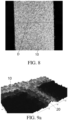
FIG. 8 is a schematic two-dimensional structural diagram of a bus electrode under a scanning electron microscope according to an embodiment of this application; -
FIG. 9a is a schematic three-dimensional structural diagram of a junction of a bus electrode and a collector electrode under a scanning electron microscope according to an embodiment of this application; and -
FIG. 9b is a schematic two-dimensional structural diagram of a junction of a bus electrode and a collector electrode under a scanning electron microscope according to an embodiment of this application. - In
FIG. 1 to FIG. 9b : 10-bus electrode, 20-collector electrode, 30-cell, and 50-mask. - To make the objectives, technical solutions, and advantages of the embodiments of this application clearer, the following clearly and completely describes the technical solutions in the embodiments of this application with reference to the accompanying drawings in the embodiments of this application. Apparently, the described embodiments are merely some embodiments of this application rather than all of the embodiments. Based on the embodiments in this application, all other embodiments obtained by a person of ordinary skill in the art without making creative efforts fall within the protection scope of this application.
- For ease of describing the technical solutions in the embodiments of this application clearly, in the embodiments of this application, the terms such as "first" and "second" are used to distinguish same or similar items having a basically same function and role. A person skilled in the art may understand that the terms such as "first" and "second" do not limit a quantity and an execution sequence. In addition, the terms such as "first" and "second" do not indicate a definite difference.
- It should be noted that, in this applications, the term such as "exemplary" or "for example" is used to represent giving an example, an illustration, or a description. Any embodiment or design scheme described as "exemplary" or "for example" in this application should not be explained as being more preferred or having more advantages than another embodiment or design scheme. Exactly, use of the term "exemplary" or "for example" is intended to present a related concept in a specific manner.
- In this application, "at least one" means one or more, and "a plurality of" means two or more. "And/or" describes an association relationship between associated objects and represents that three relationships may exist. For example, A and/or B may represent the following three cases: Only A exists, both A and B exist, and only B exists, where A and B may be singular or plural. The character "/" generally indicates an "or" relationship between the associated objects. "At least one of the following" or a similar expression thereof refers to any combination of these items, including a single item or any combination of a plurality of items. For example, at least one of a, b, or c may indicate: a, b, c, a combination of a and b, a combination of a and c, a combination of b and c, or a combination of a, b, and c, where a, b, and c may be singular or plural.
- During preparation of a solar cell, preparing electrodes on a cell is an important step. There are many processes for preparing the electrodes. When the electrodes are prepared on the cell through screen printing, a resistivity of a used silver paste generally ranges from 4×10⁻⁶ Ω·cm to 8×10⁻⁶ Ω·cm. To ensure that the prepared electrodes do not have excessively great resistance, an electrode having a large cross-sectional area needs to be prepared through the screen printing. Due to the strong fluidity of the silver paste, a prepared collector electrode generally has a large width (at present, a minimum limit of the width is 30 µm). Such a wider collector electrode will block sunlight, resulting in a low light absorption rate of the cell.
- To resolve the foregoing technical problem, an embodiment of this application provide an electrode of a solar cell. As shown in
FIG. 1 , the electrode is located on acell 30 of the solar cell. The electrode includes abus electrode 10 and acollector electrode 20 intersecting with each other, where a width of the collector electrode at any point on thecollector electrode 20 ranges from 5 µm to 30 µm; and a resistivity of each of thecollector electrode 20 and thebus electrode 10 is less than or equal to 3×10⁻⁶ Ω·cm. It should be understood that in the embodiments of this application, a thickness is a length in a direction perpendicular to thecell 30; the width is a maximum size of a length of a smaller side of an orthographic projection pattern of each of thebus electrode 10 or thecollector electrode 20 on thecell 30; and the length is a length of a larger side of the orthographic projection pattern of each of thebus electrode 10 or thecollector electrode 20 on thecell 30, namely, an extension length of each of thebus electrode 10 or thecollector electrode 20. A cross section is a cutting plane obtained by performing cutting along a direction perpendicular to the length of each of thebus electrode 10 or thecollector electrode 20. - It may be learned from the foregoing electrode structure that, the width of the collector electrode at any point on the
collector electrode 20 included in the electrode ranges from 5 µm to 30 µm. Compared with acollector electrode 20 having a width larger than 30 µm prepared through the screen printing, thecollector electrode 20 in this application has a smaller width. Because the width of thecollector electrode 20 is small, blocking to the sunlight can be greatly reduced, so that more sunlight can be incident onto thecell 30, thereby improving the conversion efficiency and an output power of the solar cell. Meanwhile, the resistivity of each of thecollector electrode 20 and thebus electrode 10 is less than or equal to 3×10⁻⁶ Ω·cm. In other words, a material of each of thecollector electrode 20 and thebus electrode 10 has good electrical conductivity. In the related art, a resistivity of a silver paste for the screen printing generally ranges from 4×10⁻⁶ Ω·cm to 8×10⁻⁶ Ω·cm. Compared with the screen printing, in this application, on one hand, acollector electrode 20 having a smaller width (the width ranges from 5 µm to 30 µm) may be prepared, reducing blocking to the sunlight. On the other hand, because the resistivity of thecollector electrode 20 in this application is small, with the same width, the same conductive effect can be achieved when a thickness of thecollector electrode 20 in this application accounts for only 0.375 to 0.75 of a thickness of the collector electrode in the screen printing, so that the thickness of thecollector electrode 20 can be reduced. In this case, the process difficulty of preparing thecollector electrode 20 can be reduced and the preparation efficiency can be improved, and materials can be saved, reducing stress applied by the electrode to thecell 30, thereby reducing cracking of thecell 30. For example, when thecollector electrode 20 is prepared through the screen printing by using a silver paste with a resistivity of 6×10⁻⁶ Ω·cm,collector electrodes 20 having the same width are prepared, and if a thickness of thecollector electrode 20 prepared through the screen printing is 20 µm, acollector electrode 20 having a thickness of 10 µm is prepared in the embodiments of this application to achieve the same conductive effect. Based on the above, by using the electrode provided in this application, the conversion efficiency and the output power of the solar cell can be improved, and materials may be saved, thereby reducing cracking. - As shown in
FIG. 1 andFIG. 5 toFIG. 7 , the electrode is located on thecell 30 of the solar cell. Specifically, as shown inFIG. 7 , the electrode may be located on acell 30 having a textured surface. In this case, thecollector electrode 20 having a small width is combined with the textured surface, so that a light trapping function of the textured surface is combined while blocking to the sunlight is reduced, thereby further improving a light absorption rate of thecell 30. During actual application, thecell 30 has a photoelectric conversion function and may be a crystalline silicon cell or an amorphous silicon cell. During actual application, a plurality ofcollector electrodes 20 may be distributed on thecell 30 in an array, and a plurality ofbus electrodes 10 may vertically intersect with the plurality ofcollector electrodes 20. - As shown in
FIG. 2 and FIG. 3 , a manner of preparing the electrode may be implemented through a patternedmask 50, where patterned content is a plurality of slits on themask 50. Specifically, the electrode is prepared through a sputtering, evaporation, or deposition process after themask 50 is adhered to thecell 30. In this case, thebus electrode 10 and thecollector electrode 20 may be formed simultaneously through the processes, namely, there is no need to prepare thebus electrode 10 and thecollector electrode 20 respectively in two processes. In addition, during preparation of the electrode through the processes, electrode materials are stacked layer by layer in the form of molecules. During formation of the electrode, the fluidity of the materials is small, so that a narrow andhigh collector electrode 20 can be formed, and the precision of a size of the electrode can be improved. - During actual application, the
mask 50 may be amask 50 including a base film and an adhesive layer. The base film includes a polymer thin film. A material of the polymer film may be a high molecular polymer. Specifically, the high molecular polymer includes but is not limited to one or more of polyethylene terephthalate (PET), a polyolefin film (PO), polyimide (PI), polyvinyl chloride (PVC), biaxially oriented polypropylene (BOPP), or the like. Further, a material of the adhesive layer includes but is not limited to one or more of silicone, acrylic glue, polyurethane, rubber, polyisobutylene, or the like. - The slits may be formed on the
mask 50 through laser grooving. Specifically, an ultra-fast pulsed laser with a picosecond-level or femtosecond-level pulse width may be used on themask 50, and grooving may further be performed on themask 50 by using a short pulsed laser with a microsecond-level or nanosecond-level pulse width, where the laser penetrates the base film and the adhesive layer of themask 50 to form the slits. - During actual application, coordinate positions of the slits may be planned on the
mask 50 in advance, and scribing and grooving are then performed at the planned coordinate positions of the slits by using the ultra-fast pulsed laser with a picosecond-level or femtosecond-level pulse width or the short pulsed laser with a microsecond-level or nanosecond-level pulse width, to form the slits and obtain the patternedmask 50. - It should be noted that, in combination with the foregoing description, the
mask 50 needs to be designed to have a high absorption rate within a certain wavelength range, so that themask 50 can efficiently absorb energy of a light source such as a laser in a process of performing patterning on themask 50 using the light source such as the laser, thereby improving the energy utilization efficiency and the patterning precision. A detailed wavelength range needs to be designed according to a used light source. - For example, during preparation of the electrode, a
mask 50 having a plurality of slit patterns and made of a PET film and a silicone layer may be aligned with and arranged on a front surface of thecell 30. Because the silicon layer is adhesive, themask 50 may be adhered to the front surface of the cell, and the electrode is then prepared by using electrode materials through a sputtering, evaporation, or deposition process. In this process, a part of the electrode materials run through the slits of themask 50 and fall onto the cell to form thecollector electrode 20 and thebus electrode 10, and the other part of electrode materials fall on themask 50 and are then removed together with themask 50, to finally form thecollector electrode 20 and thebus electrode 10 deposited on the front surface of thecell 30. - A resistivity of each of the
collector electrode 20 and thebus electrode 10 is less than or equal to 3×10⁻⁶ Ω·cm. That is, any metal with a material resistivity not higher than 3×10⁻⁶ Ω·cm can be used as the material of each of thecollector electrode 20 and thebus electrode 10. For example, the resistivity of each of thecollector electrode 20 and thebus electrode 10 may be 3×10⁻⁶ Ω·cm, 2.8×10⁻⁶ Ω·cm, 2.6×10⁻⁶ Ω·cm, 2.4×10⁻⁶ Ω·cm, 2.2×10⁻⁶ Ω·cm, 2×10⁻⁶ Ω·cm, 1.8×10⁻⁶ Ω·cm, 1.6×10⁻⁶ Ω·cm, 1.5×10⁻⁶ Ω·cm, 1.3×10⁻⁶ Ω·cm, 1×10⁻⁶ Ω·cm, or the like. - Specifically, the material of each of the
collector electrode 20 and thebus electrode 10 may include, but not limited to, one or more of silver, aluminum, or copper, and may further include one or more of nickel, chromium, tin, or titanium. In this case, the material of each of thecollector electrode 20 and thebus electrode 10 has good electrical conductivity. For example, a thickness of thecollector electrode 20 is 10 µm, and extending upward from a surface of thecell 30 in a direction perpendicular to the surface of thecell 30, namely, in a direction away from thecell 30, a part between 0 µm to 1 µm is a silver material layer, a part between 1.1 µm to 9 µm is an aluminum material layer, and a part between 9.1 µm to 10 µm is a copper material layer. Certainly, both thecollector electrode 20 and thebus electrode 10 may be made of a single material. For another example, a thickness of thebus electrode 10 is 15 µm, and extending upward from the surface of thecell 30 in the direction perpendicular to the surface of thecell 30, namely, in the direction away from thecell 30, a part between 0 µm and 1 µm is a nickel material layer, a part between 1.1 µm to 12 µm is an aluminum material layer, and a part between 12.1 µm to 15 µm is a copper material layer. For another example, the thickness of thecollector electrode 20 is 20 µm, and extending upward from the surface of thecell 30 in the direction perpendicular to the surface of thecell 30, namely, in the direction away from thecell 30, a part between 0 µm to 3.5 µm is a chromium material layer, a part between 3.6 µm to 15.5 µm is a copper material layer, and a part between 15.6 µm to 20 µm is a silver material layer. - As shown in
FIG. 5 to FIG. 7 , the width of the collector electrode at any point on thecollector electrode 20 may range from 5 µm to 30 µm, and the thickness of the collector electrode at any point on the collector electrode may range from 5 µm to 20 µm. Preferably, the width of the collector electrode at any point on thecollector electrode 20 may range from 10 µm to 20 µm, and the thickness of the collector electrode at any point on the collector electrode may range from 8 µm to 12 µm. For example, the width of the collector electrode at any point on thecollector electrode 20 may be 5 µm, 6 µm, 8 µm, 10 µm, 12 µm, 15 µm, 17 µm, 20 µm, 24 µm, 26 µm, 29 µm, 30 µm, or the like. The thickness of the collector electrode at any point on thecollector electrode 20 may be 5 µm, 6 µm, 7 µm, 8 µm, 10 µm, 11 µm, 12 µm, 13 µm, 15 µm, 16 µm, 17 µm, 18 µm, 19 µm, 20 µm, or the like. Compared with the size of thecollector electrode 20 obtained through the screen printing in the related art, the width of the collector electrode in the embodiments of this application is significantly reduced, so that the conversion efficiency can be improved based on the conversion efficiency of existing solar cells. - As shown in
FIG. 8 , a width D of the bus electrode at any point on thebus electrode 10 may range from 30 µm to 400 µm, and a thickness of the bus electrode at any point on the bus electrode may range from 3.4 µm to 29.4 µm. For example, the width D of the bus electrode at any point on thebus electrode 10 may be 30 µm, 50 µm, 100 µm, 130 µm, 150 µm, 170 µm, 200 µm, 250 µm, 270 µm, 300 µm, 330 µm, 360 µm, 370 µm, 390 µm, 400 µm, or the like. The thickness of the bus electrode at any point on thebus electrode 10 may be 3.4 µm, 5 µm, 6 µm, 8 µm, 10 µm, 13 µm, 15 µm, 17 µm, 19 µm, 20 µm, 24 µm, 25 µm, 27 µm, 28 µm, 29 µm, 29.4 µm, or the like. - As shown in
FIG. 1 ,FIG. 6 , andFIG. 7 , a ratio of the thickness to the width of the collector electrode at any point on thecollector electrode 20 ranges from 0.2 to 2. In this case, a narrow andhigh collector electrode 20 may be formed, so that acollector electrode 20 having a large cross-sectional area can be formed while a small width is ensured, thereby helping reduce the resistance of thecollector electrode 20, and improving the conversion efficiency and the output power of the solar cell. In addition, the narrow andhigh collector electrode 20 in this application can provide certain reflection for the sunlight, so that an absorption rate of thecell 30 for the sunlight can be further improved. In addition, the thickness-to-width ratio falling within this range may ensure the structure stability of the electrode, thereby avoiding a problem of collapse of the electrode after long-time use. For example, the ratio of the thickness to the width of the collector electrode at any point on thecollector electrode 20 may be 0.2, 0.22, 0.25, 0.28, 0.3, 0.4, 0.5, 0.6, 0.7, 0.8, 1, 1.1, 1.2, 1.3, 1.4, 1.5, 1.6, 1.7, 1.8, 1.9, 2, or the like. - During actual application, each
collector electrode 20 includes a first section, a second section, and a third section that are consecutive, the second section is located between the first section and the third section, and a length of the second section of eachcollector electrode 20 accounts for 75% to 85% of a total length of thecollector electrode 20; and a width error of the second section of eachcollector electrode 20 is less than or equal to 10%, where the width error is a percentage of a difference between the width of the collector electrode at any position on thecollector electrode 20 and a width average value of a section in which the position is located to the width average value of the section. In this case, the width error of the second section of thecollector electrode 20 is small, namely, a width error of a main body portion of thecollector electrode 20 is small, and the width of the collector electrode is consistent, so that the resistance and stress sudden changes of thecollector electrode 20 can be reduced, thereby ensuring constant stress and resistance of eachcollector electrode 20. For example, the width error of the second section of eachcollector electrode 20 may be 10%, 9%, 8%, 7%, 6%, 5%, 4%, 3%, 2%, 1%, 0%, or the like. - Further, the width error of the second section of each
collector electrode 20 is less than or equal to 8%. In this case, the width error of thecollector electrode 20 is further reduced, so that the precision of thecollector electrode 20 can be further improved, ensuring constant stress and resistance of eachcollector electrode 20. - Further, a width error of each
collector electrode 20 is less than or equal to 10%. In this case, for eachcollector electrode 20, both the main body portion (the second section) and theentire collector electrode 20 have a small width error. That is, the width of theentire collector electrode 20 is consistent. For example, the width error of eachcollector electrode 20 may be 10%, 9%, 8.5%, 8%, 7.5%, 7%, 6%, 5%, 4%, 3%, 2%, 1%, 0.5%, 0%, or the like. - Further, as shown in
FIG. 1 , widths of the collector electrode at all points on thecollector electrode 20 may be the same. Specifically, the width of theentire collector electrode 20 remains consistent throughout the entire collector electrode, and particularly, a width of a part of thecollector electrode 20 close to thebus electrode 10 is the same as those of other parts and is not narrowed. In this case, when the thickness of thecollector electrode 20 remains unchanged, because the widths of the collector electrode at all the points on the collector electrode are the same, it may be ensured that the resistance and stress at all the points on thecollector electrode 20 are consistent, thereby avoiding excessive current damage and uneven stress. Widths of the bus electrode at all points on thebus electrode 10 are the same. Specifically, the width of theentire bus electrode 10 remains consistent throughout the entire bus electrode, and particularly, a width of a junction with thecollector electrode 20 is the same as those of other parts and is not narrowed. In this case, when the thickness of thebus electrode 10 remains unchanged, because the widths of the bus electrode at all the points on the bus electrode are the same, it may be ensured that the resistance and stress at all the points on thebus electrode 10 are consistent, thereby avoiding excessive current damage and uneven stress. - Specifically, as shown in
FIG. 1, 3 bus electrodes 10 (A1, A2, and A3) on thecell 30 shown inFIG. 1 are selected, and widths of each bus electrode at 10 points on thebus electrode 10 are measured. Along a length direction of each bus electrode, the 10 points on thebus electrode 10 are uniformly distributed on thebus electrode 10. - As shown in
FIG. 1, 3 collector electrodes 20 (B1, B2, and B3) on thecell 30 shown inFIG. 1 are selected, and widths of each collector electrode at 10 points on thecollector electrode 20 are measured, where the 10 points on eachcollector electrode 10 are distributed along a length direction of the collector electrode. In addition, among the 10 points on the collector electrode B1, the third point to the eighth point fall within a section starting from 10% to 85% of a length of the collector electrode B1, namely, fall within a second section of the collector electrode B1 (the second section accounts for 75% of the total length). Among the 10 points on the collector electrode B2, the second point to the eighth point fall within a section starting from 10% to 90% of a length of the collector electrode B2, namely, fall within a second section of the collector electrode B2 (the second section accounts for 80% of the total length). Among the 10 points on the collector electrode B3, the second point to the ninth point fall within a section starting from 10% to 95% of a length of the collector electrode B3, namely, fall within a second section of the collector electrode B3 (the second section accounts for 85% of the total length). - In addition, 6 cells (not shown in the figure) are selected, and 1
collector electrode 20 is selected from each cell, namely, 6collector electrodes 20 are selected, which are respectively denoted as C1, C2, C3, C4, C5, and C6. 6 points are selected from eachcollector electrode 20 for measuring thicknesses and widths of the collector electrode at the 6 points. - Through actual measurement, measurement results of widths of the bus electrodes A1, A2, and A3 are shown in Table 1; and measurement results of widths of the collector electrodes B1, B2, and B3 are shown in Table 2, and measurement results of thickness-to-width ratios of the collector electrodes C1 to C6 are shown in Table 3.


Table 3 Thickness-to-width ratios of collector electrodes C1 to C6 Collector electrode Point Thickness measured value (µm) Width measured value (µm) Thickness-to-width ratio C1 First point 9.32 19.39 0.48 Second point 9.41 20.85 0.45 Third point 9.75 18.84 0.52 Fourth point 9.56 20.85 0.46 Fifth point 9.36 18.53 0.51 Sixth point 9.23 18.62 0.50 C2 First point 11.42 9.39 1.22 Second point 11.51 10.85 1.06 Third point 10.75 9.28 1.16 Fourth point 11.46 11.42 1.00 Fifth point 11.36 10.53 1.08 Sixth point 10.30 10.62 0.97 C3 First point 4.32 16.39 0.26 Second point 3.61 17.85 0.20 Third point 3.75 17.84 0.21 Fourth point 3.46 16.85 0.21 Fifth point 3.40 16.53 0.21 Sixth point 3.73 18.62 0.20 C4 First point 8.21 28.85 0.28 Second point 9.06 28.62 0.32 Third point 7.22 29.53 0.24 Fourth point 7.96 27.84 0.29 Fifth point 8.07 29.96 0.27 Sixth point 7.96 29.85 0.27 C5 First point 29.28 15.39 1.90 Second point 28.32 14.85 1.91 Third point 28.74 16.84 1.71 Fourth point 29.40 15.85 1.85 Fifth point 28.27 16.53 1.71 Sixth point 27.87 15.62 1.78 C6 First point 11.12 5.68 1.96 Second point 11.51 6.30 1.83 Third point 10.3 5.15 2.00 Fourth point 10.46 5.36 1.95 Fifth point 10.94 6.25 1.75 Sixth point 10.67 5.50 1.94 - It may be learned from Table 1 that, widths of the three
bus electrodes 10 A1 to A3 range from 200.31 µm to 209.72 µm, and a width error of each bus electrode 10 (the width error is a ratio of a difference between the width measured value and the width average value to the width average value) is less than or equal to 2%, where a maximum width error is 2%, and a minimum width error is 1%. It may be learned from Table 2 that, widths of the threecollector electrodes 20 B1 to B3 range from 18.63 µm to 22.99 µm, and a width error of eachcollector electrode 20 is less than or equal to 10%, where a minimum width error is 3%, and a maximum width error is 10%. The width error at each point on each of thebus electrode 10 and thecollector electrode 20 is less than or equal to 10%. It may be learned that, each of thebus electrode 10 and thecollector electrode 20 in the embodiments of this application has a consistent width and a small width error. - It may be learned from Table 2 through analysis that, a width of the second section starting from the third point to the eight point of the collector electrode B1 ranges from 18.63 µm to 22.68 µm, and a width error of the second section ranges from 3% to 10%. It may be learned that, the width error of the second section of the collector electrode B1 may be less than or equal to 10%. A width of the second section starting from the second point to the eighth point of the collector electrode B2 ranges from 19.47 µm to 22.18 µm, and a width error of the second section ranges from 1% to 8%. It may be learned that, the width error of the second section of the collector electrode B2 may be less than or equal to 8%. A width of the second section starting from the second point to the ninth point of the collector electrode B3 ranges from 18.93 µm to 22.99 µm, and a width error of the second section ranges from 1% to 10%. It may be learned that, the width error of the second section of the collector electrode B3 may be less than or equal to 10%.
- It may be learned from Table 3 that, a thickness-to-width ratio of the collector electrode C1 ranges from 0.46 to 0.52, a thickness-to-width ratio of the collector electrode C2 ranges from 0.97 to 1.22, a thickness-to-width ratio of the collector electrode C3 ranges from 0.2 to 0.26, a thickness-to-width ratio of the collector electrode C4 ranges from 0.24 to 0.32, a thickness-to-width ratio of the collector electrode C5 ranges from 1.71 to 1.91, and a thickness-to-width ratio of the collector electrode C6 ranges from 1.75 to 2. It may be learned that, the thickness-to-width ratio of each collector electrode in this application ranges from 0.2 to 2.
- It may be learned from
FIG. 6 ,FIG. 9a , andFIG. 9b that, the width of eachcollector electrode 10 is consistent, and the width of eachbus electrode 20 is also consistent. Thecollector electrode 20 has a narrow and thick morphology, which helps reduce blocking to light, thereby increasing light reflection and improving the light absorption rate of thecell 30. - As shown in
FIG. 2 , thebus electrode 10 has a large width, and a cross-sectional shape of thebus electrode 10 may be a rectangle. As shown inFIG. 3a and FIG. 3b , thecollector electrode 20 has a plurality of cross-sectional shapes, and during actual application, a corresponding cross-sectional shape may be selected according to a requirement of the solar cell. The cross-sectional shape of thecollector electrode 20 is a shape of a cross section obtained by performing cutting on thecollector electrode 20 along a direction perpendicular to a length direction of thecollector electrode 20. In some embodiments, as shown inFIG. 3a , the cross-sectional shape of thecollector electrode 20 may be a triangle. In this case, thetriangular collector electrode 20 provides reflection for the incident sunlight, so that thecollector electrode 20 has a light trapping function, and the absorption rate for the sunlight is improved. During specific implementation, the cross-sectional shape of thecollector electrode 20 may be adjusted according to a width and a depth of each of the slits on themask 50. By setting themask 50 with a large thickness, within specified process time, thethick mask 50 provides great blocking to the electrode materials, thereby facilitating formation of thetriangular collector electrode 20. A width-to-thickness ratio of thetriangular collector electrode 20 may range from 1.8 to 2.2. - In some embodiments, as shown in
FIG. 3b , the cross-sectional shape of thecollector electrode 20 may be a trapezoid, and a top surface of thecollector electrode 20 is an arc surface. The cross-sectional shape of thecollector electrode 20 is similar to steamed bread. In this case, width changes at all the points on thecollector electrode 20 are small, and material coverage is good, so that problems such as a gate with poor contact can be avoided. During specific implementation, compared with thetriangular collector electrode 20, thecollector electrode 20 with a steamed bread-shaped cross section may be formed by reducing the thickness of themask 50 properly. A ratio of a thickness to a width of thecollector electrode 20 may range from 0.8 to 1.2. - As shown in
FIG. 4 , an angle α exists between aside surface 21 of thecollector electrode 20 and thecell 30 along a length direction of thecollector electrode 20. In this case, theside surface 21 of thecollector electrode 20 is inclined relative to thecell 30. Theinclined side surface 21 of thecollector electrode 20 can support thecollector electrode 20, thereby improving the stability of thecollector electrode 20. Especially, when thecollector electrode 20 is narrow and thick, the stability of the collector electrode is relatively poor, and theinclined side surface 21 may assist in fixing thecollector electrode 20, thereby improving the stability of the collector electrode and reducing a probability that thecollector electrode 20 collapses. - As shown in
FIG. 1 , a gap exists between every twoadjacent collector electrodes 20 along the same track, and a length of the gap ranges from 400 µm to 2000 µm. The length of the gap is a distance between twoadjacent collector electrodes 20 along the same track. In this case, a coverage area of thecollector electrode 20 on thecell 30 may be reduced, to improve the light absorption rate of thecell 30. For example, the length of the gap may be 400 µm, 500 µm, 600 µm, 700 µm, 800 µm, 900 µm, 1000 µm, 1100 µm, 1300 µm, 1500 µm, 1600 µm, 1800 µm, 1900 µm, 2000 µm, or the like. - An embodiment of this application further provides a solar cell. The solar cell includes the electrode of a solar cell described above. For beneficial effects of the solar cell, reference may be made to the beneficial effects of the electrode, and details are not described herein again.
- Although this application has been described with reference to the embodiments herein, however, in a process of implementing this application claimed for protection, a person skilled in the art may understand and implement other variations of the embodiments of this application by viewing the accompanying drawings, the disclosed content, and the appended claims. In the claims, the term "comprising" does not exclude other components or steps, and the term "a" or "an" does not exclude a plurality. Some measures are recorded in dependent claims that are different from each other, but this does not mean that these measures cannot be combined to produce a better effect.
- The foregoing described apparatus embodiments are merely examples. The units described as separate parts may or may not be physically separate, and the parts displayed as units may or may not be physical units, may be located in one position, or may be distributed on a plurality of network units. Some or all the modules may be selected according to an actual requirement to implement the objective of the solutions of the embodiments. A person of ordinary skill in the art may understand and implement this application without creative efforts.
- "An embodiment", "embodiment", or "one or more embodiments" mentioned in the specification means that particular features, structures, or characteristics described with reference to the embodiment or embodiments may be comprised in at least one embodiment of this application. In addition, it should be noted that the term example "in an embodiment" herein does not necessarily indicate a same embodiment.
- In the specification provided herein, a plurality of specific details are described. However, it can be understood that the embodiments of this application can be practiced without these specific details. In some examples, well-learned methods, structures, and technologies are not shown in detail so as not to obscure the understanding of this specification.
- Finally, it should be noted that, the foregoing embodiments are only used for describing the technical solutions of this application rather than limiting this application. Although this application is described in detail with reference to the foregoing embodiments, a person of ordinary skill in the art should understand that modifications may be still made to the technical solutions described in the foregoing embodiments or equivalent replacements may be made to some technical features thereof. These modifications or replacements do not cause the essence of corresponding technical solutions to depart from the spirit and scope of the technical solutions in the embodiments of this application.
Claims (13)
- An electrode of a solar cell, comprising a collector electrode and a bus electrode intersecting with each other, wherein a width of the collector electrode at any point on the collector electrode ranges from 5 µm to 30 µm; and a resistivity of each of the collector electrode and the bus electrode is less than or equal to 3×10⁻⁶ Ω·cm.
- The electrode of a solar cell according to claim 1, wherein the width the collector electrode at any point on the collector electrode ranges from 10 µm to 20 µm; and a width of the bus electrode at any point on the bus electrode ranges from 30 µm to 400 µm.
- The electrode of a solar cell according to claim 1, wherein a material of each of the collector electrode and the bus electrode comprises one or more of silver, aluminum, or copper.
- The electrode of a solar cell according to claim 1, wherein a ratio of a thickness to the width of the collector electrode at any point on the collector electrode ranges from 0.2 to 2.
- The electrode of a solar cell according to claim 1, whereineach collector electrode comprises a first section, a second section, and a third section that are consecutive, the second section is located between the first section and the third section, and a length of the second section of each collector electrode accounts for 75% to 85% of a total length of the collector electrode; and a width error of the second section of each collector electrode is less than or equal to 10%, whereinthe width error is a percentage of a difference between a width of the collector electrode at any position on the collector electrode and a width average value of a section in which the position is located to the width average value of the section.
- The electrode of a solar cell according to claim 5, wherein the width error of the second section of each collector electrode is less than or equal to 8%.
- The electrode of a solar cell according to claim 5, wherein a width error of each collector electrode is less than or equal to 10%.
- The electrode of a solar cell according to claim 5, wherein widths of the collector electrode at all points on the collector electrode are the same, and widths of the bus electrode at all points on the bus electrode are the same.
- The electrode of a solar cell according to any one of claims 1 to 8, wherein a cross-sectional shape of the collector electrode is a triangle; or
a cross-sectional shape of the collector electrode is a trapezoid, and a top surface of the collector electrode is an arc surface. - The electrode of a solar cell according to any one of claims 1 to 8, wherein
an angle exists between a side surface of the collector electrode and a cell along a length direction of the collector electrode. - The electrode of a solar cell according to any one of claims 1 to 8, wherein a gap exists between every two adjacent collector electrodes along the same track, and a length of the gap ranges from 400 µm to 2000 µm.
- The electrode of a solar cell according to any one of claims 1 to 8, wherein the electrode is prepared through a sputtering, evaporation, or deposition process after a mask is adhered to a cell.
- A solar cell, comprising the electrode of a solar cell according to any one of claims 1 to 12.
Applications Claiming Priority (2)
| Application Number | Priority Date | Filing Date | Title |
|---|---|---|---|
| CN202111614565.5A CN116364788A (en) | 2021-12-27 | 2021-12-27 | A kind of solar cell and its electrode |
| PCT/CN2022/122293 WO2023124324A1 (en) | 2021-12-27 | 2022-09-28 | Solar cell and electrodes thereof |
Publications (2)
| Publication Number | Publication Date |
|---|---|
| EP4459681A1 true EP4459681A1 (en) | 2024-11-06 |
| EP4459681A4 EP4459681A4 (en) | 2025-04-09 |
Family
ID=86914430
Family Applications (1)
| Application Number | Title | Priority Date | Filing Date |
|---|---|---|---|
| EP22913589.2A Pending EP4459681A4 (en) | 2021-12-27 | 2022-09-28 | SOLAR CELL AND ELECTRODES FOR IT |
Country Status (5)
| Country | Link |
|---|---|
| US (1) | US20250063849A1 (en) |
| EP (1) | EP4459681A4 (en) |
| CN (1) | CN116364788A (en) |
| AU (1) | AU2022428735B2 (en) |
| WO (1) | WO2023124324A1 (en) |
Family Cites Families (14)
| Publication number | Priority date | Publication date | Assignee | Title |
|---|---|---|---|---|
| JPH05235388A (en) * | 1992-02-24 | 1993-09-10 | Mitsubishi Electric Corp | Method and apparatus for forming low resistance linear pattern, and solar cell |
| US8322025B2 (en) * | 2006-11-01 | 2012-12-04 | Solarworld Innovations Gmbh | Apparatus for forming a plurality of high-aspect ratio gridline structures |
| KR101089088B1 (en) * | 2008-09-12 | 2011-12-06 | 주식회사 엘지화학 | Solar cell front electrode with minimal power loss and solar cell comprising same |
| KR100993511B1 (en) * | 2008-11-19 | 2010-11-12 | 엘지전자 주식회사 | Solar cell and manufacturing method thereof |
| FR2989520B1 (en) * | 2012-04-11 | 2014-04-04 | Commissariat Energie Atomique | METHOD FOR PRODUCING A HETEROJUNCTION PHOTOVOLTAIC CELL |
| RU2636405C2 (en) * | 2012-10-04 | 2017-11-23 | Син-Эцу Кемикал Ко., Лтд. | Method of producing solar cell |
| CN202977437U (en) * | 2012-12-18 | 2013-06-05 | 英利能源(中国)有限公司 | Solar cell grid line electrode and solar cell piece |
| WO2014185225A1 (en) * | 2013-05-13 | 2014-11-20 | 株式会社カネカ | Solar cell module and method for producing same |
| CN106816481A (en) * | 2015-12-02 | 2017-06-09 | 钧石(中国)能源有限公司 | A kind of preparation method of heterojunction solar battery |
| GB201613051D0 (en) * | 2016-07-28 | 2016-09-14 | Landa Labs (2012) Ltd | Applying an electrical conductor to a substrate |
| CN106784045B (en) * | 2016-12-28 | 2019-05-07 | 中国电子科技集团公司第十八研究所 | A multi-level grid line layout structure and method of a solar cell |
| WO2019003818A1 (en) * | 2017-06-26 | 2019-01-03 | 株式会社カネカ | Solar cell, method for producing same, and solar cell module |
| CN210110814U (en) * | 2019-09-20 | 2020-02-21 | 浙江晶科能源有限公司 | A solar cell electrode grid line structure |
| CN112531040B (en) * | 2020-11-30 | 2022-09-16 | 浙江鸿禧能源股份有限公司 | A grid line structure of a photovoltaic cell and a manufacturing method thereof |
-
2021
- 2021-12-27 CN CN202111614565.5A patent/CN116364788A/en active Pending
-
2022
- 2022-09-28 EP EP22913589.2A patent/EP4459681A4/en active Pending
- 2022-09-28 WO PCT/CN2022/122293 patent/WO2023124324A1/en not_active Ceased
- 2022-09-28 US US18/720,871 patent/US20250063849A1/en active Pending
- 2022-09-28 AU AU2022428735A patent/AU2022428735B2/en active Active
Also Published As
| Publication number | Publication date |
|---|---|
| US20250063849A1 (en) | 2025-02-20 |
| AU2022428735B2 (en) | 2025-12-18 |
| AU2022428735A1 (en) | 2024-07-18 |
| CN116364788A (en) | 2023-06-30 |
| WO2023124324A1 (en) | 2023-07-06 |
| EP4459681A4 (en) | 2025-04-09 |
Similar Documents
| Publication | Publication Date | Title |
|---|---|---|
| US4292092A (en) | Laser processing technique for fabricating series-connected and tandem junction series-connected solar cells into a solar battery | |
| US12349501B2 (en) | Photovoltaic cell and photovoltaic module | |
| JP2744847B2 (en) | Improved solar cell and method for manufacturing the same | |
| US20140230894A1 (en) | Bifacial crystalline silicon solar panel with reflector | |
| EP3588581A1 (en) | Back-contact solar cell string and preparation method therefor, module and system | |
| US20220278246A1 (en) | Bifacial crystalline silicon solar panel with reflector | |
| EP2325896A2 (en) | Front electrode for solar cell which minimizes power loss, and solar cell including the same | |
| CN105529373A (en) | A front electrode of a crystalline silicon solar cell | |
| EP3608974A1 (en) | Cell string formed by connecting n-type ibc solar cells in spliced-sheet manner, preparation method therefor, assembly and system | |
| CN118099239B (en) | Back contact battery with series structure, battery module and manufacturing method thereof | |
| CN217691184U (en) | Thin film solar cell | |
| KR102366935B1 (en) | Solar cell and solar cell module including the same | |
| US20250063849A1 (en) | Solar cell and electrodes thereof | |
| CN116867293A (en) | Perovskite solar cell and preparation method thereof | |
| CN121487470A (en) | A foldable, integrated perovskite solar cell and its fabrication method | |
| US20220077339A1 (en) | Solar cell panel | |
| JP4287560B2 (en) | Method for manufacturing thin film photoelectric conversion module | |
| CN110459620A (en) | A kind of preparation method of metal grid line | |
| WO2023124615A1 (en) | Mask and solar cell | |
| WO2013027591A1 (en) | Solar cell and solar cell module | |
| JP2011009307A (en) | Thin-film solar cell and method of manufacturing the same | |
| CN212570983U (en) | Battery piece | |
| CN221468267U (en) | Perovskite photovoltaic module and battery module | |
| KR102379388B1 (en) | Solar cell and solar cell panel including the same | |
| CN112993164A (en) | Matrix type large-area perovskite battery and preparation method thereof |
Legal Events
| Date | Code | Title | Description |
|---|---|---|---|
| STAA | Information on the status of an ep patent application or granted ep patent |
Free format text: STATUS: THE INTERNATIONAL PUBLICATION HAS BEEN MADE |
|
| PUAI | Public reference made under article 153(3) epc to a published international application that has entered the european phase |
Free format text: ORIGINAL CODE: 0009012 |
|
| STAA | Information on the status of an ep patent application or granted ep patent |
Free format text: STATUS: REQUEST FOR EXAMINATION WAS MADE |
|
| 17P | Request for examination filed |
Effective date: 20240605 |
|
| AK | Designated contracting states |
Kind code of ref document: A1 Designated state(s): AL AT BE BG CH CY CZ DE DK EE ES FI FR GB GR HR HU IE IS IT LI LT LU LV MC MK MT NL NO PL PT RO RS SE SI SK SM TR |
|
| REG | Reference to a national code |
Ref country code: DE Ref legal event code: R079 Free format text: PREVIOUS MAIN CLASS: H01L0031022400 Ipc: H10F0077200000 |
|
| DAV | Request for validation of the european patent (deleted) | ||
| DAX | Request for extension of the european patent (deleted) | ||
| A4 | Supplementary search report drawn up and despatched |
Effective date: 20250311 |
|
| RIC1 | Information provided on ipc code assigned before grant |
Ipc: H10F 77/00 20250101ALI20250305BHEP Ipc: H10F 77/20 20250101AFI20250305BHEP |