EP4456100A1 - Kondensator und verfahren zur herstellung davon - Google Patents
Kondensator und verfahren zur herstellung davon Download PDFInfo
- Publication number
- EP4456100A1 EP4456100A1 EP22918797.6A EP22918797A EP4456100A1 EP 4456100 A1 EP4456100 A1 EP 4456100A1 EP 22918797 A EP22918797 A EP 22918797A EP 4456100 A1 EP4456100 A1 EP 4456100A1
- Authority
- EP
- European Patent Office
- Prior art keywords
- foil
- thickness
- cathode foil
- lead
- out terminal
- Prior art date
- Legal status (The legal status is an assumption and is not a legal conclusion. Google has not performed a legal analysis and makes no representation as to the accuracy of the status listed.)
- Pending
Links
Images








Classifications
-
- H—ELECTRICITY
- H01—ELECTRIC ELEMENTS
- H01G—CAPACITORS; CAPACITORS, RECTIFIERS, DETECTORS, SWITCHING DEVICES, LIGHT-SENSITIVE OR TEMPERATURE-SENSITIVE DEVICES OF THE ELECTROLYTIC TYPE
- H01G9/00—Electrolytic capacitors, rectifiers, detectors, switching devices, light-sensitive or temperature-sensitive devices; Processes of their manufacture
- H01G9/004—Details
- H01G9/008—Terminals
- H01G9/012—Terminals specially adapted for solid capacitors
-
- H—ELECTRICITY
- H01—ELECTRIC ELEMENTS
- H01G—CAPACITORS; CAPACITORS, RECTIFIERS, DETECTORS, SWITCHING DEVICES, LIGHT-SENSITIVE OR TEMPERATURE-SENSITIVE DEVICES OF THE ELECTROLYTIC TYPE
- H01G9/00—Electrolytic capacitors, rectifiers, detectors, switching devices, light-sensitive or temperature-sensitive devices; Processes of their manufacture
- H01G9/004—Details
- H01G9/008—Terminals
-
- H—ELECTRICITY
- H01—ELECTRIC ELEMENTS
- H01G—CAPACITORS; CAPACITORS, RECTIFIERS, DETECTORS, SWITCHING DEVICES, LIGHT-SENSITIVE OR TEMPERATURE-SENSITIVE DEVICES OF THE ELECTROLYTIC TYPE
- H01G13/00—Apparatus specially adapted for manufacturing capacitors; Processes specially adapted for manufacturing capacitors not provided for in groups H01G4/00 - H01G11/00
- H01G13/006—Apparatus or processes for applying terminals
-
- H—ELECTRICITY
- H01—ELECTRIC ELEMENTS
- H01G—CAPACITORS; CAPACITORS, RECTIFIERS, DETECTORS, SWITCHING DEVICES, LIGHT-SENSITIVE OR TEMPERATURE-SENSITIVE DEVICES OF THE ELECTROLYTIC TYPE
- H01G9/00—Electrolytic capacitors, rectifiers, detectors, switching devices, light-sensitive or temperature-sensitive devices; Processes of their manufacture
- H01G9/004—Details
- H01G9/04—Electrodes or formation of dielectric layers thereon
- H01G9/042—Electrodes or formation of dielectric layers thereon characterised by the material
- H01G9/0425—Electrodes or formation of dielectric layers thereon characterised by the material specially adapted for cathode
-
- H—ELECTRICITY
- H01—ELECTRIC ELEMENTS
- H01G—CAPACITORS; CAPACITORS, RECTIFIERS, DETECTORS, SWITCHING DEVICES, LIGHT-SENSITIVE OR TEMPERATURE-SENSITIVE DEVICES OF THE ELECTROLYTIC TYPE
- H01G9/00—Electrolytic capacitors, rectifiers, detectors, switching devices, light-sensitive or temperature-sensitive devices; Processes of their manufacture
- H01G9/004—Details
- H01G9/04—Electrodes or formation of dielectric layers thereon
- H01G9/048—Electrodes or formation of dielectric layers thereon characterised by their structure
- H01G9/055—Etched foil electrodes
-
- H—ELECTRICITY
- H01—ELECTRIC ELEMENTS
- H01G—CAPACITORS; CAPACITORS, RECTIFIERS, DETECTORS, SWITCHING DEVICES, LIGHT-SENSITIVE OR TEMPERATURE-SENSITIVE DEVICES OF THE ELECTROLYTIC TYPE
- H01G9/00—Electrolytic capacitors, rectifiers, detectors, switching devices, light-sensitive or temperature-sensitive devices; Processes of their manufacture
- H01G9/15—Solid electrolytic capacitors
- H01G9/151—Solid electrolytic capacitors with wound foil electrodes
-
- Y—GENERAL TAGGING OF NEW TECHNOLOGICAL DEVELOPMENTS; GENERAL TAGGING OF CROSS-SECTIONAL TECHNOLOGIES SPANNING OVER SEVERAL SECTIONS OF THE IPC; TECHNICAL SUBJECTS COVERED BY FORMER USPC CROSS-REFERENCE ART COLLECTIONS [XRACs] AND DIGESTS
- Y02—TECHNOLOGIES OR APPLICATIONS FOR MITIGATION OR ADAPTATION AGAINST CLIMATE CHANGE
- Y02E—REDUCTION OF GREENHOUSE GAS [GHG] EMISSIONS, RELATED TO ENERGY GENERATION, TRANSMISSION OR DISTRIBUTION
- Y02E60/00—Enabling technologies; Technologies with a potential or indirect contribution to GHG emissions mitigation
- Y02E60/13—Energy storage using capacitors
Definitions
- the present disclosure relates to a capacitor including a cathode foil including a carbon layer, and a method for manufacturing the same.
- a capacitor includes an anode foil, a cathode foil, and a separator disposed between the anode foil and the cathode foil, and can store electricity.
- a basic capacitor including a basic cathode foil formed only of an aluminum foil is known.
- a capacitor including a cathode foil including a carbon layer has been known (for example, Patent Literature 1). The carbon layer has an effect of increasing electrostatic capacitance of the cathode foil, for example.
- Patent Literature 1 JP2006-80111A
- An electrode foil is connected to a lead-out terminal by connection methods such as stitch connection.
- connection methods such as stitch connection.
- a stitch needle is inserted into the lead-out terminal and the electrode foil overlapped each other from the lead-out terminal side, a terminal hole and a terminal piece are formed in the lead-out terminal, and a through hole and a foil piece are formed in the electrode foil.
- the terminal piece protrudes from a back surface of the electrode foil through the through hole of the electrode foil.
- the terminal piece and the foil piece are pressed and overlapped on the back surface of the electrode foil.
- the stitch connection is formed, and the electrode foil is connected to the lead-out terminal.
- the carbon layer is formed by, for example, applying a slurry mainly composed of carbon particles and a binder to a surface of an aluminum foil and bonding the carbon particles to each other by the binder.
- the binder contained in the carbon layer causes a stress toward the outside around a pressing portion against a pressing force against the carbon layer, and the cathode foil including the carbon layer is easier to stretch than a basic cathode foil formed of only a metal foil such as an aluminum foil.
- the carbon layer stretches when the terminal piece and the foil piece are pressed, and a base material of the cathode foil stretches following the carbon layer.
- the cathode foil having the carbon layer is easier to stretch than the basic cathode foil in the stitch connecting process. Since the pressing force is weakened when the cathode foil stretches, there is a problem that it is more difficult to connect the lead-out terminal to the cathode foil by the stitch connecting process.
- Patent Literature 1 does not disclose or suggest such a problem, and the configuration disclosed in Patent Literature 1 cannot solve such a problem.
- An object of the present disclosure is to provide a stitch connection structure suitable for a cathode foil including a carbon layer, for example.
- a capacitor includes a cathode foil including a carbon layer disposed at a surface of a base material foil, and a lead-out terminal including a flat portion connected to the cathode foil by stitch connection at a stitch connection portion.
- a thickness of the stitch connection portion is equal to or less than a total thickness of a thickness of the cathode foil and a thickness of the flat portion.
- a terminal end of the lead-out terminal may protrude from a foil end of the cathode foil, may coincide with the foil end, or may overlap the cathode foil at an interval of 0.1 millimeter or less or 0.5 millimeter or more from the foil end.
- the thickness of the stitch connection portion may be less than the total thickness.
- an absolute value of a difference between the thickness of the stitch connection portion and the total thickness may be 0.02 millimeter or less.
- the thickness of the flat portion may be 0.18 millimeter or more and 0.35 millimeter or less.
- the thickness of the cathode foil may be 0.01 millimeter or more and 0.06 millimeter or less.
- a method for manufacturing a capacitor includes a step of producing a cathode foil including a carbon layer disposed at a surface of a base material foil, and a step of disposing a flat portion of a lead-out terminal on a terminal arrangement surface of the cathode foil, and connecting the flat portion to the cathode foil at a stitch connection portion by a stitch connecting process so that a thickness of the stitch connection portion is equal to or less than a total thickness of a thickness of the cathode foil and a thickness of the flat portion.
- the flat portion may be connected to the cathode foil so that a terminal end of the lead-out terminal protrudes from a foil end of the cathode foil, or in the step of connecting the flat portion to the cathode foil, the flat portion may be connected to the cathode foil so that the terminal end coincides with the foil end or overlaps the cathode foil at an interval of 0.1 millimeter or less or 0.5 millimeter or more from the foil end.
- a method for manufacturing a capacitor includes: a step of grasping a thickness of a cathode foil including a carbon layer disposed at a surface of a base material foil and a thickness of a flat portion of a lead-out terminal; a step of determining a thickness of a stitch connection portion so that the thickness of the stitch connection portion is equal to or less than a total thickness of the thickness of the cathode foil and the thickness of the flat portion; a step of adjusting a stitch connection device so that the stitch connection device crushes the stitch connection portion until the thickness of the stitch connection portion becomes the determined thickness; and a step of connecting the flat portion to the cathode foil by the adjusted stitch connection device.
- the stitch connection device may be adjusted so that a terminal end of the lead-out terminal protrudes from a foil end of the cathode foil, or in the step of adjusting the stitch connection device, the stitch connection device may be adjusted so that the terminal end coincides with the foil end or overlaps the cathode foil at an interval of 0.1 millimeter or less or 0.5 millimeter or more from the foil end.
- Fig. 1 illustrates an example of a cathode foil and a terminal connection portion of a lead-out terminal of a capacitor according to a first embodiment.
- Fig. 2 illustrates an example of an end surface of the cathode foil.
- the terminal connection portion includes a connection place where the lead-out terminal 4 is connected to the cathode foil 6 by stitch connection, that is, a stitch connection portion 10 and a peripheral portion thereof.
- a shaded portion in A of FIG. 1 represents the stitch connection portion 10.
- B of FIG. 1 is a cross-sectional view taken along a line IB-IB in A of FIG. 1 .
- the stitch connection portion 10 is an area where a terminal piece 24 is disposed, and refers to an area including a portion where the lead-out terminal 4, the cathode foil 6, a foil piece 28, and the terminal piece 24 are stacked from the terminal hole 22.
- the capacitor 2 is an example of an electronic component, and is, for example, an electrolytic capacitor.
- the capacitor 2 includes, for example, a capacitor element (not illustrated), the lead-out terminal 4, and an electrolyte, a sealing member, and an exterior case, which are not illustrated.
- the capacitor element includes the cathode foil 6, an anode foil, and a separator.
- the cathode foil 6, the anode foil, and the separator are overlapped and wound so that the separator is disposed between the cathode foil 6 and the anode foil, thereby forming a winding element.
- the winding element forms the capacitor element.
- the cathode foil 6 constitutes an electrode on a cathode side of the capacitor 2.
- the cathode foil 6 is, for example, a strip-shaped foil, and includes a base material foil 12 and a carbon layer 14.
- Examples of the base material foil 12 include valve metal foils such as an aluminum foil, a tantalum foil, a niobium foil, a titanium foil, a hafnium foil, a zirconium foil, a zinc foil, a tungsten foil, a bismuth foil, and an antimony foil. As illustrated in Fig.
- a surface of the base material foil 12 has unevenness 16 formed by etching, for example, that is, recesses 16-1 and protrusions 16-2, and a surface area of the base material foil 12 is enlarged.
- the surface of the base material foil 12 may include, for example, a tunnel-like or sponge-like etching pit, and the tunnel-like or sponge-like etching pit may form the recess 16-1 and the protrusion 16-2.
- the carbon layers 14 are disposed on both surfaces of the base material foil 12, for example.
- the carbon layer 14 may be disposed only on one surface of the base material foil 12. As illustrated in Fig. 2 , the carbon layer 14 partially enters the inside of the recesses 16-1 of the unevenness 16, and thus closely adheres to and engaged with the unevenness 16 of the base material foil 12. That is, the carbon layer 14 has a surface shape that engages with the unevenness 16.
- the carbon layer 14 is disposed outside the base material foil 12, and the cathode foil 6 has a two-layer structure including the base material foil 12 and the carbon layer 14 or a three-layer structure in which the carbon layers 14 are disposed on both surfaces of the base material foil 12.
- the carbon layer 14 contains a carbon material as a main material, and further contains a binder and a dispersant as additives.
- Examples of a carbon material include activated carbon, carbon black, carbon nanohorn, amorphous carbon, natural graphite, artificial graphite, graphitized Ketjen black, mesoporous carbon, and fibrous carbon.
- the activated carbon is produced from, for example, natural plant tissues such as coconut shells, synthetic resins such as phenol, and those derived from fossil fuels such as coal, coke, or pitch.
- Examples of the carbon black include Ketjen black, acetylene black, channel black, thermal black, or the like.
- the fibrous carbon is a carbon nanotube, a carbon nanofiber, or the like.
- the carbon nanotube may be a single-walled carbon nanotube with a single layer of graphene sheets, or a multi-walled carbon nanotube (MWCNT) with two or more layers of graphene sheets rolled coaxially to form a multilayered tube wall.
- MWCNT multi-walled carbon nanotube
- the carbon material is preferably carbon black which is spherical carbon.
- carbon black which is spherical carbon.
- the carbon material is also preferably a mixture containing spherical carbon and graphite.
- the graphite is, for example, natural graphite, artificial graphite, graphitized Ketjen black, or the like, and has a shape such as a scaly shape, a scale shape, a lump shape, a soil shape, a spherical shape, or a flake shape.
- the graphite is preferably scaly or flaky, and an aspect ratio of a short diameter to a long diameter of the graphite is preferably in a range of 1: 5 to 1: 100.
- the scaly or flaky graphite having the aspect ratio described above pushes spherical carbon into the recess 16-1 of the unevenness 16 such as an etching pit, and a part of the carbon layer 14 can be formed up to the etching pit. Therefore, the carbon layer 14 can firmly adhere to the base material foil 12 by an anchor effect.
- an average particle diameter of the graphite is 6 micrometers (hereinafter, referred to as " ⁇ m") or more and 10 ⁇ m or less, an effect of preventing a decrease in electrostatic capacitance due to a high temperature environmental load can be obtained.
- the average particle diameter of the graphite is 6 ⁇ m or less, it is possible to increase the electrostatic capacitance of the capacitor 2 while preventing a decrease in the electrostatic capacitance due to a high temperature environmental load.
- the average particle diameter of the graphite is 6 ⁇ m or less, the graphite is easily retained in the carbon layer 14, and an addition amount of the binder can be reduced. By reducing the addition amount of the binder, a ratio of the carbon material increases. Therefore, electric resistance of the cathode foil 6 can be reduced, and the equivalent series resistance of the capacitor 2 can be reduced.
- the numerical value of the above average particle diameter is a numerical value based on the median diameter, so-called D50.
- a mass ratio of graphite to the mixture of graphite and spherical carbon is, for example, in a range of 25% or more and 90% or less, in order to obtain the effect of the combined use of graphite and spherical carbon.
- the binder is, for example, a resin-based binder such as styrene butadiene rubber, polyvinylidene fluoride, or polytetrafluoroethylene, and binds a carbon material.
- the dispersant is, for example, sodium carboxymethyl cellulose.
- the carbon layer 14 is made of, for example, an aqueous solution in which spherical carbon is dispersed. The dispersant can disperse the carbon material in the aqueous solution.
- the anode foil constitutes an electrode on an anode side of the capacitor 2.
- the anode foil is, for example, a valve metal foil such as a tantalum foil or an aluminum foil, and is, for example, a strip-shaped foil.
- a surface of the anode foil has unevenness formed by etching, for example, and includes a dielectric oxide film formed by chemical conversion treatment, for example.
- the unevenness formed by etching has, for example, a porous structure.
- the separator is disposed between the anode foil and the cathode foil 6 to prevent a short circuit between the anode foil and the cathode foil 6.
- the separator is an insulating material and includes a kraft, and may include other separator members such as Manila hemp, esparto, hump, rayon, cellulose, and a mixed material thereof.
- the cathode foil 6 is connected to the lead-out terminal 4 by stitch connection.
- the anode foil is connected to another lead-out terminal (not illustrated) (hereinafter referred to as a "lead-out terminal 4" for convenience) by stitch connection or other connection methods.
- the lead-out terminal 4 protrudes from one end surface of the capacitor element.
- the lead-out terminal 4 is made of, for example, a highly conductive metal such as aluminum.
- the lead-out terminal 4 includes, for example, an aluminum wire and a metal wire 17 ( Fig. 7 ), and the aluminum wire and the metal wire 17 are connected by arc welding or the like.
- the aluminum wire includes a substantially cylindrical round rod portion and a flat portion 18 formed by press working or the like of the round rod portion, and the round rod portion has an inclined portion whose thickness linearly decreases to a thickness of the flat portion 18 on the flat portion 18 side.
- the flat portion 18 is overlapped on the cathode foil 6 and is connected to the cathode foil 6 by stitch connection to form the stitch connection portion 10. That is, the flat portion 18 is connected to the cathode foil 6 by stitch connection at the stitch connection portion 10.
- the electrolyte contains at least an electrolytic solution and is filled in voids and separators in the capacitor element.
- the sealing member is formed of, for example, insulating rubber.
- the sealing member has an insertion hole at a position corresponding to the lead-out terminal 4.
- the lead-out terminal 4 penetrates the insertion hole of the sealing member and is exposed to the outside of the capacitor 2.
- the exterior case is, for example, a bottomed tubular aluminum case.
- the capacitor element and a part of the lead-out terminal 4 are inserted into the exterior case together with the electrolyte.
- the sealing member is installed in an opening portion of the exterior case to seal the inside of the exterior case. That is, the capacitor element and a part of the lead-out terminal 4 are sealed in the exterior case.
- the lead-out terminal 4 passes through the through hole of the sealing member and protrudes from the sealing member.
- the flat portion 18 is connected to the cathode foil 6 by stitch connection, and the stitch connection portion 10 is formed.
- the flat portion 18 includes the terminal hole 22 and the terminal piece 24, and the cathode foil 6 includes the through hole and the foil piece 28.
- the terminal hole 22, the terminal piece 24, the through hole, and the foil piece 28 are formed by inserting a stitch needle 46 ( Fig. 6 ) from the lead-out terminal 4 side.
- the terminal hole 22 is disposed at a position overlapping the through hole.
- the terminal piece 24 and the foil piece 28 are folded back by pressing from the cathode foil 6 side, and are pressed against a back surface of the cathode foil 6, that is, an opposing surface of a terminal arrangement surface.
- the stitch connection portion 10 is an area where the flat portion 18 and the cathode foil 6 are connected to each other, and is defined as, for example, an area where the terminal piece 24 is disposed in A of FIG. 1 .
- the flat portion 18 and the terminal piece 24 that form a fold sandwich the cathode foil 6 and the foil piece 28 from two surfaces, for example, upper and lower surfaces.
- a thickness T1 of the stitch connection portion 10 is equal to or less than the total thickness Tt of a thickness T2 of the cathode foil 6 and a thickness T3 of the flat portion 18, and is expressed by the following formula (1).
- T 1 ⁇ Tt T2 + T3
- the equivalent series resistance of the capacitor 2 can be reduced and stabilized, and when the thickness T1 is less than the total thickness Tt, the equivalent series resistance of the capacitor 2 is further reduced and further stabilized.
- the thickness T2 of the cathode foil 6 and the thickness T3 of the flat portion 18 can be freely set, and may be appropriately set according to the specification of the capacitor 2, for example.
- the thickness T2 of cathode foil 6 is, for example, 0.01 millimeter (hereinafter, referred to as "mm") or more and 0.06 mm or less
- the thickness T3 of flat portion 18 is, for example, 0.18 mm or more and 0.35 mm or less.
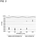
- Fig. 3 is a graph illustrating an example of a relationship between a difference ⁇ T between the thickness T1 and the total thickness Tt and the equivalent series resistance (ESR).
- Fig. 4 is a graph illustrating an example of a relationship between the difference ⁇ T and a yield strength of the foil.
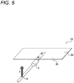
- Fig. 5 is a diagram illustrating an example of a method for measuring the yield strength of the foil.
- the difference ⁇ T is expressed by the following formula (2).
- ⁇ T T1 ⁇ Tt
- a carbon layer-containing foil represents the cathode foil 6 including the carbon layer 14.
- the cathode foil 6 having the thickness T2 of 0.02 mm and the lead-out terminal 4 including the flat portion 18 having the thickness T3 of 0.23 mm are used. That is, when the total thickness Tt is 0.25 mm and the thickness T1 of the stitch connection portion 10 is 0.25 mm, the difference ⁇ T is 0.00 mm.
- the graph illustrated in Fig. 3 includes equivalent series resistance data of a capacitor using a basic cathode foil for comparison.
- the basic cathode foil represents a cathode foil not including a carbon layer, and a thickness of the basic cathode foil is 0.02 mm, which is the same as the thickness T2 of the cathode foil 6 in this test.
- the equivalent series resistance of the capacitor 2 using the carbon layer-containing foil is smaller than the equivalent series resistance of the capacitor using the basic cathode foil having the same difference ⁇ T, and the variation is small. That is, by satisfying a requirement of "T1 ⁇ Tt" which is not superior to the capacitor using the basic cathode foil, the capacitor 2 using the carbon layer-containing foil can obtain reduced and stable equivalent series resistance.
- the yield strength of the carbon layer-containing foil increases until the difference ⁇ T decreases to -0.02 mm.
- the thickness T1 of the stitch connection portion 10 is preferably equal to or less than the total thickness Tt, and the absolute value (
- the graph illustrated in B of Fig. 4 illustrates the yield strength of the previously described basic cathode foil for comparison.
- the yield strength of the basic cathode foil is highest when the difference ⁇ T is 0.00 mm, and decreases as the difference ⁇ T becomes smaller than 0.00 mm. That is, by satisfying requirements of "T1 ⁇ Tt" and "
- Fig. 5 illustrates the example of the method for measuring the yield strength of the foil.
- a tensile force F that is perpendicular to a foil 32 and is directed above a second main surface 36 of the foil 32 is applied to a tensile point X of the lead-out terminal 4 attached to a first main surface 34 of the foil 32.
- the foil 32 is a carbon layer-containing foil, that is, the cathode foil 6 or the basic cathode foil.
- the yield strength of the foil is defined as, for example, the magnitude of the tensile force F when a crack occurs in the foil 32.
- the test for the yield strength of the foil is not limited to the test illustrated in Fig. 5 as long as the magnitude of the yield strength of the foil can be relatively evaluated.
- the tensile point X may be fixed in a series of tests, and may be freely set.
- Manufacturing steps of the capacitor 2 are an example of a method for manufacturing the capacitor according to the present disclosure, and includes, for example, a producing step of the anode foil, a producing step of the cathode foil 6, a producing step of the separator, a grasping step of the thickness T2 of the cathode foil 6 and the thickness T3 of the flat portion 18 of the lead-out terminal 4, a determining step of the thickness T1 of the stitch connection portion 10, an adjusting step of a stitch connection device 40 ( Fig. 6 ), a connecting step of the lead-out terminal 4 to the electrode foil (hereinafter, referred to as a "connecting step of the lead-out terminal"), a producing step of the capacitor element, and a sealing step of the capacitor element.
- a producing step of the anode foil includes, for example, a producing step of the anode foil, a producing step of the cathode foil 6, a producing step of the separator, a grasping step of the thickness T2 of the cathode foil 6
- the surface of a valve metal foil such as a tantalum foil or an aluminum foil is etched to form unevenness at the surface of the valve metal foil.
- the valve metal foil after the etching treatment is subjected to a chemical conversion treatment to form a dielectric oxide film at the surface of the valve metal foil.
- the valve metal foil is etched by applying a current to the valve metal foil immersed in a chloride aqueous solution such as hydrochloric acid or sodium chloride.
- the applied current may be a direct current or an alternating current.
- valve metal foil In the chemical conversion treatment of the valve metal foil, for example, a voltage is applied to the valve metal foil immersed in an electrolytic solution containing a solution of ammonium borate, ammonium borate, ammonium phosphate, ammonium adipate, or the like. The formed valve metal foil is cut to produce an anode foil.
- the base material foil 12 is produced by etching the surface of a valve metal foil such as an aluminum foil, a tantalum foil, a niobium foil, a titanium foil, a hafnium foil, a zirconium foil, a zinc foil, a tungsten foil, a bismuth foil, or an antimony foil to form the unevenness 16 at the surface of the valve metal foil.
- a valve metal foil such as an aluminum foil, a tantalum foil, a niobium foil, a titanium foil, a hafnium foil, a zirconium foil, a zinc foil, a tungsten foil, a bismuth foil, or an antimony foil.
- the etching on the cathode foil 6 side may be the same as or different from the etching on the anode foil side.
- the carbon layer 14 is formed on the valve metal foil after the etching treatment, that is, the base material foil 12, and the base material foil 12 on which the carbon layer 14 is formed is
- the carbon layer 14 is produced as follows.
- the carbon material, the binder, and the dispersant described above are added to a diluent, and the mixture is mixed with by a dispersion treatment such as a mixer, jet mixing (jet collision), ultracentrifugation, or ultrasonic treatment to form a slurry.
- the binder is added in an amount necessary for bonding the carbon material, for example, and the dispersant is added in an amount necessary for dispersing the carbon material, for example. Therefore, addition amounts of the binder and the dispersant are smaller than the addition amount of the carbon material.
- the graphite When graphite is used as the carbon material, the graphite may be pulverized by a pulverizer such as a bead mill or a ball mill, and the average particle diameter of the graphite may be adjusted before addition to the diluent.
- a pulverizer such as a bead mill or a ball mill
- the diluent examples include alcohols, hydrocarbon-based solvents, aromatic solvents, amide-based solvents, water, and mixtures thereof.
- the alcohol is, for example, methanol, ethanol, or 2-propanol.
- the amide-based solvent is, for example, N-methyl-2-pyrrolidone (NMP) or N, N-dimethylformamide (DMF).
- the slurry is applied to the valve metal foil after the etching treatment, that is, the base material foil 12. Since the unevenness 16 is formed on the base material foil 12, the carbon material enters the unevenness 16 to improve adhesion. After the slurry is dried to volatilize the solvent to form the carbon layer 14, the carbon layer 14 is pressed. When a press working step is added in addition to the formation of the unevenness 16, the carbon material can be pushed into fine pores of the unevenness 16, the carbon material can be deformed along an unevenness surface of the unevenness 16, and adhesion and the fixing property between the carbon layer 14 and the base material foil 12 are further improved.
- the carbon material contains graphite
- the graphite is aligned by pressing, and the graphite is deformed along the unevenness 16 of the base material foil 12. Further, when the graphite is pressed against the unevenness 16, the spherical carbon is pushed into the inside of the recess 16-1 such as the fine pore of the base material foil 12. As a result, the slurry closely adheres to the base material foil 12, and the carbon layer 14 closely adhering to the base material foil 12 is obtained.
- the carbon material is only spherical carbon, in particular, spherical carbon having an average primary particle diameter of 100 nanometers or less is used, so that the spherical carbon easily enters the recess 16-1, and thus the interface resistance between the carbon layer 14 and the base material foil 12 easily decreases.
- spherical carbon having an average primary particle diameter of 100 nanometers or less is used, so that the spherical carbon easily enters the recess 16-1, and thus the interface resistance between the carbon layer 14 and the base material foil 12 easily decreases.
- graphite since graphite is not contained, a static friction coefficient of the surface of the carbon layer 14 is improved, and when the terminal piece 24 is pressed against the foil piece 28, the terminal piece 24 does not easily slip, and stitch connection with stable connectivity is obtained.
- the separator member described above is cut to produce the separator.
- the thickness T2 of the cathode foil 6 and the thickness T3 of the flat portion 18 of the lead-out terminal 4 are grasped.
- these dimension public values are grasped as grasped values of the thicknesses T2 and T3.
- the thicknesses T2 and T3 may be actually measured, and the measurement values obtained by the measurement may be grasped as grasped values of the thicknesses T2 and T3.
- the total thickness Tt is obtained by adding the grasped value of the thickness T2 and the grasped value of the thickness T3.
- the thickness T1 is determined such that the thickness T1 is equal to or less than the total thickness Tt.
- the thickness T1 is preferably determined such that the absolute value of the difference ⁇ T is 0.02 mm or less or the thickness T2 of the cathode foil 6 or less.
- the stitch connection device 40 is adjusted such that the stitch connection device 40 crushes the stitch connection portion 10 until the determined thickness T1 is reached.
- the adjustment of the stitch connection device 40 includes adjustment of device setting such as distance setting.
- the lead-out terminal 4 is connected to each of the cathode foil 6 and the anode foil.
- the stitch connection device 40 is used.
- the stitch connection device 40 includes, for example, a first die 42, a second die 44, a stitch needle 46, and a forming die 48.
- the cathode foil 6 is placed on the first die 42 such as a lower die, and the lead-out terminal 4 is overlapped on an upper surface of the cathode foil 6, that is, the terminal arrangement surface.
- the second die 44 such as an upper die is placed on an upper surface of the lead-out terminal 4. Therefore, the cathode foil 6 and the lead-out terminal 4 are sandwiched between the first die 42 and the second die 44 and held by the first die 42 and the second die 44.
- the cathode foil 6 placed on the first die 42 is the cathode foil 6 before the through hole and the foil piece 28 are formed, and the lead-out terminal 4 overlapped on the cathode foil 6 is the lead-out terminal 4 before the terminal hole 22 and the terminal piece 24 are formed.
- the first die 42 has a through hole 50
- the second die 44 has a through hole 52.
- the through hole 50 has a hole shape slightly larger than a cross-sectional shape of the forming die 48.
- the through hole 52 has a hole shape slightly larger than a cross-sectional shape of the stitch needle 46.
- the through hole 52 is smaller than the through hole 50 and is disposed directly above the through hole 50.
- the stitch needle 46 has, for example, an acute and pyramidal tip end portion in a columnar shaft portion, and is disposed above the through hole 52.
- the stitch needle 46 is lowered in a direction of an arrow illustrated in A of Fig. 6 , and as illustrated in B of Fig. 6 , the stitch needle 46 is inserted into the lead-out terminal 4 and the cathode foil 6 from the lead-out terminal 4 side.
- the stitch needle 46 By inserting the stitch needle 46, the through hole and the foil piece 28 are formed in the cathode foil 6, and the terminal hole 22 and the terminal piece 24 are formed in the lead-out terminal 4.
- the lowered stitch needle 46 is raised, and the stitch needle 46 is pulled out from the lead-out terminal 4 and the cathode foil 6.
- the forming die 48 has, for example, a flat pressing surface on an upper side thereof and is disposed below the through hole 50.
- the forming die 48 is raised in a direction of an arrow illustrated in B of Fig. 6 , and the pressing surface presses the lead-out terminal 4 and the cathode foil 6, particularly the terminal piece 24 and the foil piece 28 from the cathode foil 6 side.
- the terminal piece 24 and the foil piece 28 are sandwiched between the second die 44 and the forming die 48.
- the terminal piece 24 and the foil piece 28 are folded back by pressing, and the lead-out terminal 4 is connected to the cathode foil 6.
- the adjusted stitch connection device 40 adjusts the thickness T1 of the stitch connection portion 10 to the total thickness Tt or less.
- the pressing surface of the forming die 48 before being raised is indicated by a broken line.
- the stitch connection device 40 raises the forming die 48 by a movement distance L and crushes the stitch connection portion 10 by the second die 44 and the forming die 48.
- the thickness T1 of the crushed stitch connection portion 10 coincides with a distance S between the second die 44 and the forming die 48.
- the movement distance L or the distance S is an example of device setting such as distance setting of the stitch connection device 40.
- the movement distance L or the distance S is set in the stitch connection device 40, and the thickness T1 of the stitch connection portion 10 is adjusted.
- the distance setting of the stitch connection device 40 may be, for example, a crushing distance of the stitch connection portion 10.
- the crushing distance is defined as a distance from a reference surface, in which a contact surface formed by contact between the first die 42 and the cathode foil 6 is defined as the reference surface.
- the stitch connection device 40 raises the pressing surface of the forming die 48 to the reference surface, and the thickness T1 is adjusted to the total thickness Tt.
- the stitch connection device 40 raises the pressing surface of the forming die 48 to a position 0.02 mm above the contact surface, and adjusts the thickness T1 to a thickness 0.02 mm thinner than the total thickness Tt.
- the adjustment of the stitch connection device 40 may be any of position adjustment of an upper limit switch of a cylinder for raising the forming die 48, adjustment of a rotation amount of a screw of a screw type elevator, position adjustment of a stopper for stopping the raising of the forming die 48 by contact, and adjustment by computer control using set value data, or may be other adjustment.
- the connecting step of the lead-out terminal 4 to the anode foil may be the same as or different from the connecting step of the lead-out terminal 4 to the cathode foil 6.
- the setting of the crushing distance may be different.
- the carbon layer is not formed at the surface, there is little possibility that the anode foil is easily stretched by a stress toward the outside around pressing portions of the terminal piece 24 and the foil piece 28, unlike the cathode foil 6 which is the carbon layer-containing foil.
- unevenness is formed at the surface of the valve metal foil as described above, and a dielectric oxide film is formed on the unevenness by chemical conversion treatment.
- the dielectric oxide film is hard, and extensibility and flexibility of the anode foil decrease.
- a surface area of the anode foil is increased by surface-increasing processing at a higher magnification, but the area of the dielectric oxide film is also increased as the capacity of the anode foil is increased, and as a result, the anode foil becomes fragile and hardened, and flexibility of the material itself is likely to be extremely reduced.
- a first separator is disposed between the anode foil and the cathode foil 6, and a second separator is disposed outside the anode foil or the cathode foil 6.
- the anode foil, the cathode foil 6, and the first and second separators are wound to produce the capacitor element.
- the capacitor element impregnated with an electrolyte such as an electrolytic solution is inserted into the exterior case, and a sealing member is attached to the opening portion of the exterior case to produce the capacitor 2.
- the capacitor 2 according to the second embodiment has the configuration of the capacitor 2 described in the first embodiment, for example.
- the contents described in the first embodiment are incorporated into the second embodiment by reference, and the description in the second embodiment is omitted.
- Fig. 7 illustrates an example of a lead-out terminal and a cathode foil of a capacitor according to the second embodiment.
- the configuration illustrated in Fig. 7 is an example, and a technology of the present disclosure is not limited to such a configuration.
- the positions of a terminal end 66 and a press mark end 68 of the lead-out terminal 4 are adjusted or managed with respect to a foil end 62 and a foil end 64 of the cathode foil 6, respectively, and a foil crack of the cathode foil 6 is prevented.
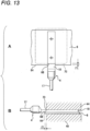
- the press mark is a trace formed on the lead-out terminal 4, in particular, the flat portion 18 by pressing of the die such as the second die 44 and the forming die 48 in the connecting step of the lead-out terminal described above, and the press mark end 68 is a trace formed on the flat portion 18 of the lead-out terminal 4 by pressing of a die end portion 70 ( Figs. 12 and 13 ) of the second die 44. That is, the press mark end 68 represents a boundary of an area to be pressed.
- the press mark end 68 is formed, for example, on the metal wire 17 side of the flat portion 18.
- the terminal end 66 of lead-out terminal 4 is retracted from foil end 62 of cathode foil 6, for example.
- a distance Y1 (unit: mm) between the terminal end 66 and the foil end 62 is preferably 0.1 or less or 0.5 or more.
- the distance Y1 may be 0.0, and the terminal end 66 may coincide with the foil end 62. That is, the distance Y1 is adjusted or managed in a range represented by the following formula (3), for example. 0.0 ⁇ Y1 ⁇ 0.1 , or 0 .5 ⁇ Y1
- the maximum value of the distance Y1 may be set from a viewpoint of the structure or performance of the capacitor 2.
- the lead-out terminal 4 may protrude from the foil end 62. The protruding lead-out terminal 4 prevents the foil crack of the cathode foil 6.
- the press mark end 68 of the lead-out terminal 4 is retracted from the foil end 64 of the cathode foil 6, for example.
- a distance Z1 (unit: mm) between the press mark end 68 and the foil end 64 is preferably 0.1 or less.
- the distance Z1 may be 0.0, and the press mark end 68 may coincide with the foil end 64. That is, the distance Z1 is adjusted or managed in a range represented by the following formula (4), for example. 0.0 ⁇ Z1 ⁇ 0.1
- the press mark end 68 may protrude from the foil end 64.
- the press mark end 68 is adjusted or managed so as to protrude from the foil end 64, the foil crack of the cathode foil 6 is prevented.
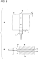
- Fig. 8 illustrates the result of the first experiment, and illustrates the occurrence of foil cracks at the distance Y1 or Y2 (hereinafter referred to as "distance Y1 or Y2").
- the foil crack is defined as a crack extending from the foil end 62 of the cathode foil 6 to the terminal piece 24 of the stitch connection portion 10.
- the foil crack may be formed in the cathode foil 6 by pressing against the lead-out terminal 4 and the cathode foil 6 in the connecting step of the lead-out terminal described above, for example.
- a crack that does not correspond to the definition described above, for example, a crack that does not reach the terminal piece 24, is not treated as a foil crack.
- a distance Y2 (unit: mm) is defined as a distance between the terminal end 66 of the lead-out terminal 4 protruding from the foil end 62 of the cathode foil 6 and the foil end 62.
- the first experiment is an experiment for confirming the presence or absence of a foil crack when the distances Y1 and Y2 between the terminal end 66 and the foil end 62 are changed under a condition of the stitch connection of the lead-out terminal 4 to the cathode foil 6 including the carbon layer 14.
- the distance Y1 is a value within the range of the above formula (3). That is, the terminal end 66 coincides with the foil end 62, and overlaps the cathode foil 6 at an interval of 0.1 mm or less or 0.5 mm or more from the foil end 62.
- the lead-out terminal 4 overlaps up to the foil end 62 of the cathode foil 6. Therefore, in the connecting step of the lead-out terminal, as illustrated in B of Fig. 9 , the foil end 62 of the cathode foil 6 is sandwiched and fixed between the second die 44 and the forming die 48 via the lead-out terminal 4. As described above, the cathode foil 6 including the carbon layer 14 is easier to stretch than the basic cathode foil (that is, the cathode foil not including the carbon layer).
- the terminal end 66 protrudes from the foil end 62, it is estimated that the elongation of the foil end 62 is prevented by fixing the foil end 62, and it is estimated that the foil crack of the cathode foil 6 is prevented.
- the terminal end 66 coincides with the foil end 62, and when the terminal end 66 is slightly (for example, 0.1 mm) retracted from the foil end 62, it is estimated that the elongation of the foil end 62 is prevented by fixing the foil end 62 or the vicinity of the foil end 62, and it is estimated that the foil crack of the cathode foil 6 is prevented.
- the cathode foil 6 protrudes from the lead-out terminal 4 to form a protruding foil end portion 72.
- the protruding foil end portion 72 is in a free state without being sandwiched between the second die 44 and the forming die 48 via the lead-out terminal 4.
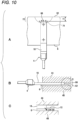
- the distance of the protruding foil end portion 72 that is, the distance Y1 is, for example, 0.5 mm or more and an area of the protruding foil end portion 72 is wide
- the stress propagated from the forming die 48 and the lead-out terminal 4 to the cathode foil 6 is dispersed in a buffer area 74 including the protruding foil end portion 72 and a peripheral area thereof, and it is estimated that the foil crack of the cathode foil 6 is prevented.
- Arrows in A and C of Fig. 10 indicate the stress propagated to the cathode foil 6.
- the distance of the protruding foil end portion 72 that is, the distance Y1 is, for example, 0.2 mm or more and 0.4 mm or less, and the area of the protruding foil end portion 72 is narrow, it is estimated that the stress propagated from the forming die 48 and the lead-out terminal 4 to the cathode foil 6 is propagated to the protruding foil end portion 72, and it is estimated that the elongation of the cathode foil 6 due to the stress increases. Therefore, it is estimated that the cathode foil 6 is cracked.
- Fig. 11 illustrates a result of a second experiment, and illustrates the occurrence of foil cracks at the distance Z1 or Z2 (hereinafter referred to as "distance Z1 or Z2").
- the definition of the foil crack is the same as the definition of the foil crack in the first experiment except that the foil end 62 is changed to the foil end 64.
- a crack that does not correspond to the definition described above, for example, a crack that does not reach the terminal piece 24, is not treated as a foil crack.
- the distance Z2 (unit: mm) is defined as a distance between the press mark end 68 of the lead-out terminal 4 protruding from the foil end 64 of the cathode foil 6 and the foil end 64.
- the second experiment is an experiment for confirming the presence or absence of a foil crack when the distances Z1 and Z2 between the press mark end 68 and the foil end 64 are changed under a condition of the stitch connection of the lead-out terminal 4 to the cathode foil 6 including the carbon layer 14.
- the distance Z1 is a value within the range of the above formula (4). That is, the press mark end 68 coincides with the foil end 64, and overlaps the cathode foil 6 at an interval of 0.1 mm or less from the foil end 64.
- the press mark end 68 protrudes from the foil end 64
- the pressed area of the lead-out terminal 4 overlaps up to the foil end 64 of the cathode foil 6.
- the foil end 64 of the cathode foil 6 is sandwiched and fixed between the second die 44 and the forming die 48 via the lead-out terminal 4.
- the cathode foil 6 including the carbon layer 14 is easier to stretch than the basic cathode foil (that is, the cathode foil not including the carbon layer).
- the foil crack may be prevented, and when the distance Z1 is, for example, 0.5 mm or more, the foil crack may be prevented.
- the result of the second experiment does not suggest that the same results as 0.2 mm and 0.3 mm are obtained at the distance Z1 of 0.4 mm or more.
- the foil crack of the cathode foil 6 does not affect the performance and vibration resistance of the capacitor 2.
- the vibration resistance of the capacitor 2 is affected, for example. Therefore, the vibration resistance of the capacitor 2 can be improved by adjusting or managing the distances Y1 and Y2 between the terminal end 66 and the foil end 62 so as to satisfy the condition (1) or the condition (2), and the vibration resistance of the capacitor 2 can be improved by adjusting or managing the distances Z1 and Z2 between the press mark end 68 and the foil end 64 so as to satisfy the condition (3) or the condition (4). Even in use in an environment where vibration is applied, for example, the equivalent series resistance of the capacitor 2 can be maintained for a long period.
- Manufacturing steps of the capacitor 2 are an example of a method for manufacturing the capacitor according to the present disclosure, and includes, for example, the producing step of the anode foil, the producing step of the cathode foil 6, the producing step of the separator, the grasping step of the thickness T2 of the cathode foil 6 and the thickness T3 of the flat portion 18 of the lead-out terminal 4, the determining step of the thickness T1 of the stitch connection portion 10, the adjusting step of the stitch connection device 40, the connecting step of the lead-out terminal, the producing step of the capacitor element, and the sealing step of the capacitor element.
- the producing step of the anode foil, the producing step of the cathode foil 6, the producing step of the separator, the grasping step of the thickness T2 of the cathode foil 6 and the thickness T3 of the flat portion 18 of the lead-out terminal 4, the determining step of the thickness T1 of the stitch connection portion 10, the producing step of the capacitor element, and the sealing step of the capacitor element are the same as those described in the first embodiment. Description of these steps described in the first embodiment will be omitted.
- a process similar to the adjusting step of the stitch connection device 40 in the first embodiment is performed, and an adjustment process of the distances Y1 and Y2 and the distances Z1 and Z2 is performed.
- an arrangement position of the lead-out terminal 4 with respect to the cathode foil 6 is adjusted so as to satisfy the condition (1) or the condition (2), for example, and in the adjustment process of the distances Z1 and Z2, the arrangement position of the second die 44 with respect to the cathode foil 6, in particular, the arrangement position of the die end portion 70 is adjusted so that the press mark end 68 to be formed on the lead-out terminal 4 by the pressing of the die satisfies the condition (3) or the condition (4) after the connecting step of the lead-out terminal, for example.
- the distances Y1 and Y2 and the distances Z1 and Z2 are adjusted by, for example, adjusting the position of an alignment device of the lead-out terminal 4 or the cathode foil 6, adjusting the position of the second die 44 or the forming die 48, or adjusting the positions of a plurality of these.
- the distances Y1 and Y2 are adjusted by adjusting the position of the lead-out terminal 4.
- the distances Z1 and Z2 are adjusted by adjusting the position of the second die 44, particularly the position of the die end portion 70.
- the distances Y1 and Y2 and the distances Z1 and Z2 are basically the same before and after the connecting step of the lead-out terminal. Therefore, in the adjusting step of the stitch connection device 40, the conditions (1) to (4) in the capacitor 2 can be used.
- the connecting step of the lead-out terminal is the same as the connecting step of the lead-out terminal in the first embodiment, except that the lead-out terminal 4 is connected to the cathode foil 6 in a state where the distances Y1 and Y2 and the distances Z1 and Z2 are adjusted.
- a press mark is formed on the lead-out terminal 4 by the pressing of the second die 44, and the press mark end 68 is formed at a position where the die end portion 70 abuts.
- the technique of the present disclosure can be used for connection between a cathode foil including a carbon layer and a lead-out terminal and for a capacitor including the same, which is useful.
Landscapes
- Engineering & Computer Science (AREA)
- Power Engineering (AREA)
- Microelectronics & Electronic Packaging (AREA)
- Manufacturing & Machinery (AREA)
- Chemical & Material Sciences (AREA)
- Materials Engineering (AREA)
- Electric Double-Layer Capacitors Or The Like (AREA)
- Fixed Capacitors And Capacitor Manufacturing Machines (AREA)
Applications Claiming Priority (3)
| Application Number | Priority Date | Filing Date | Title |
|---|---|---|---|
| JP2022000950 | 2022-01-06 | ||
| JP2022054271A JP7815926B2 (ja) | 2022-01-06 | 2022-03-29 | コンデンサおよびその製造方法 |
| PCT/JP2022/046597 WO2023132212A1 (ja) | 2022-01-06 | 2022-12-19 | コンデンサおよびその製造方法 |
Publications (2)
| Publication Number | Publication Date |
|---|---|
| EP4456100A1 true EP4456100A1 (de) | 2024-10-30 |
| EP4456100A4 EP4456100A4 (de) | 2025-08-27 |
Family
ID=87073555
Family Applications (1)
| Application Number | Title | Priority Date | Filing Date |
|---|---|---|---|
| EP22918797.6A Pending EP4456100A4 (de) | 2022-01-06 | 2022-12-19 | Kondensator und verfahren zur herstellung davon |
Country Status (4)
| Country | Link |
|---|---|
| US (1) | US20250079089A1 (de) |
| EP (1) | EP4456100A4 (de) |
| KR (1) | KR20240134879A (de) |
| WO (1) | WO2023132212A1 (de) |
Family Cites Families (6)
| Publication number | Priority date | Publication date | Assignee | Title |
|---|---|---|---|---|
| JP3401976B2 (ja) * | 1995-02-24 | 2003-04-28 | 松下電器産業株式会社 | アルミ電解コンデンサの製造方法 |
| JP4654637B2 (ja) | 2004-09-07 | 2011-03-23 | パナソニック株式会社 | アルミ電解コンデンサの製造方法 |
| JP2009130338A (ja) * | 2007-11-28 | 2009-06-11 | Elna Co Ltd | アルミニウム電極箔に対するタブ端子の接続方法およびアルミニウム電解コンデンサ並びに固体電解コンデンサ |
| JP5402475B2 (ja) * | 2009-09-30 | 2014-01-29 | 日本ケミコン株式会社 | 電解コンデンサの製造方法 |
| JP6953724B2 (ja) * | 2017-01-25 | 2021-10-27 | 日本ケミコン株式会社 | コンデンサおよびその製造方法 |
| JP7404848B2 (ja) * | 2019-12-18 | 2023-12-26 | 日本ケミコン株式会社 | 電解コンデンサの製造方法 |
-
2022
- 2022-12-19 WO PCT/JP2022/046597 patent/WO2023132212A1/ja not_active Ceased
- 2022-12-19 EP EP22918797.6A patent/EP4456100A4/de active Pending
- 2022-12-19 KR KR1020247022218A patent/KR20240134879A/ko active Pending
- 2022-12-19 US US18/726,123 patent/US20250079089A1/en active Pending
Also Published As
| Publication number | Publication date |
|---|---|
| US20250079089A1 (en) | 2025-03-06 |
| EP4456100A4 (de) | 2025-08-27 |
| WO2023132212A1 (ja) | 2023-07-13 |
| KR20240134879A (ko) | 2024-09-10 |
Similar Documents
| Publication | Publication Date | Title |
|---|---|---|
| Skunik et al. | Improved capacitance characteristics during electrochemical charging of carbon nanotubes modified with polyoxometallate monolayers | |
| KR102320546B1 (ko) | 전극, 그 전극을 사용한 전기 이중층 캐패시터 및 전극의 제조 방법 | |
| KR20170137028A (ko) | 에너지 저장 디바이스를 위한 나노구조 전극 | |
| KR20210018201A (ko) | 전극체, 전극체를 구비하는 전해 콘덴서 및 전극체의 제조 방법 | |
| CN116235265B (zh) | 电解电容器及电解电容器的制造方法 | |
| US20130070389A1 (en) | Electrode for energy storage and method for manufacturing the same | |
| JP5855493B2 (ja) | エネルギ貯蔵体の電極及びその製造方法 | |
| EP4456100A1 (de) | Kondensator und verfahren zur herstellung davon | |
| US20240321524A1 (en) | Capacitor | |
| JP7815926B2 (ja) | コンデンサおよびその製造方法 | |
| CN118525345A (zh) | 电容器及其制造方法 | |
| JP7586215B2 (ja) | コンデンサおよびその製造方法 | |
| JP2007200979A (ja) | 電気二重層キャパシタ | |
| WO2024034640A1 (ja) | コンデンサおよびその製造方法 | |
| JP7782161B2 (ja) | コンデンサおよびその製造方法 | |
| JP2023146859A (ja) | コンデンサおよびその製造方法 | |
| JP7806474B2 (ja) | コンデンサおよびその製造方法 | |
| JP2024016384A (ja) | コンデンサおよびその製造方法 | |
| JP7604930B2 (ja) | 電解コンデンサ | |
| KR102016520B1 (ko) | 고전압 슈퍼커패시터 및 그 제조방법 | |
| JP2024170017A (ja) | コンデンサおよびその製造方法 | |
| WO2024135578A1 (ja) | コンデンサ、ならびにコンデンサの製造方法および使用方法 | |
| JP2024170016A (ja) | コンデンサおよびその製造方法 | |
| JP2024087207A (ja) | コンデンサ、およびコンデンサの製造方法 | |
| JP2010087313A (ja) | 電気二重層キャパシタ用電極 |
Legal Events
| Date | Code | Title | Description |
|---|---|---|---|
| STAA | Information on the status of an ep patent application or granted ep patent |
Free format text: STATUS: THE INTERNATIONAL PUBLICATION HAS BEEN MADE |
|
| PUAI | Public reference made under article 153(3) epc to a published international application that has entered the european phase |
Free format text: ORIGINAL CODE: 0009012 |
|
| STAA | Information on the status of an ep patent application or granted ep patent |
Free format text: STATUS: REQUEST FOR EXAMINATION WAS MADE |
|
| 17P | Request for examination filed |
Effective date: 20240725 |
|
| AK | Designated contracting states |
Kind code of ref document: A1 Designated state(s): AL AT BE BG CH CY CZ DE DK EE ES FI FR GB GR HR HU IE IS IT LI LT LU LV MC ME MK MT NL NO PL PT RO RS SE SI SK SM TR |
|
| DAV | Request for validation of the european patent (deleted) | ||
| DAX | Request for extension of the european patent (deleted) | ||
| A4 | Supplementary search report drawn up and despatched |
Effective date: 20250728 |
|
| RIC1 | Information provided on ipc code assigned before grant |
Ipc: H01G 9/008 20060101AFI20250722BHEP Ipc: H01G 9/00 20060101ALI20250722BHEP Ipc: H01G 13/00 20130101ALI20250722BHEP Ipc: H01G 9/055 20060101ALN20250722BHEP Ipc: H01G 9/042 20060101ALN20250722BHEP Ipc: H01G 9/15 20060101ALN20250722BHEP |