EP4455731A1 - Messvorrichtung - Google Patents
Messvorrichtung Download PDFInfo
- Publication number
- EP4455731A1 EP4455731A1 EP22910730.5A EP22910730A EP4455731A1 EP 4455731 A1 EP4455731 A1 EP 4455731A1 EP 22910730 A EP22910730 A EP 22910730A EP 4455731 A1 EP4455731 A1 EP 4455731A1
- Authority
- EP
- European Patent Office
- Prior art keywords
- exposure
- pulse width
- light
- measurement device
- periods
- Prior art date
- Legal status (The legal status is an assumption and is not a legal conclusion. Google has not performed a legal analysis and makes no representation as to the accuracy of the status listed.)
- Pending
Links
Images


Classifications
-
- G—PHYSICS
- G01—MEASURING; TESTING
- G01S—RADIO DIRECTION-FINDING; RADIO NAVIGATION; DETERMINING DISTANCE OR VELOCITY BY USE OF RADIO WAVES; LOCATING OR PRESENCE-DETECTING BY USE OF THE REFLECTION OR RERADIATION OF RADIO WAVES; ANALOGOUS ARRANGEMENTS USING OTHER WAVES
- G01S17/00—Systems using the reflection or reradiation of electromagnetic waves other than radio waves, e.g. lidar systems
- G01S17/88—Lidar systems specially adapted for specific applications
- G01S17/89—Lidar systems specially adapted for specific applications for mapping or imaging
- G01S17/894—3D imaging with simultaneous measurement of time-of-flight at a 2D array of receiver pixels, e.g. time-of-flight cameras or flash lidar
-
- G—PHYSICS
- G01—MEASURING; TESTING
- G01S—RADIO DIRECTION-FINDING; RADIO NAVIGATION; DETERMINING DISTANCE OR VELOCITY BY USE OF RADIO WAVES; LOCATING OR PRESENCE-DETECTING BY USE OF THE REFLECTION OR RERADIATION OF RADIO WAVES; ANALOGOUS ARRANGEMENTS USING OTHER WAVES
- G01S17/00—Systems using the reflection or reradiation of electromagnetic waves other than radio waves, e.g. lidar systems
- G01S17/02—Systems using the reflection of electromagnetic waves other than radio waves
- G01S17/06—Systems determining position data of a target
- G01S17/08—Systems determining position data of a target for measuring distance only
- G01S17/10—Systems determining position data of a target for measuring distance only using transmission of interrupted, pulse-modulated waves
- G01S17/18—Systems determining position data of a target for measuring distance only using transmission of interrupted, pulse-modulated waves wherein range gates are used
-
- G—PHYSICS
- G01—MEASURING; TESTING
- G01S—RADIO DIRECTION-FINDING; RADIO NAVIGATION; DETERMINING DISTANCE OR VELOCITY BY USE OF RADIO WAVES; LOCATING OR PRESENCE-DETECTING BY USE OF THE REFLECTION OR RERADIATION OF RADIO WAVES; ANALOGOUS ARRANGEMENTS USING OTHER WAVES
- G01S7/00—Details of systems according to groups G01S13/00, G01S15/00, G01S17/00
- G01S7/48—Details of systems according to groups G01S13/00, G01S15/00, G01S17/00 of systems according to group G01S17/00
- G01S7/483—Details of pulse systems
- G01S7/486—Receivers
- G01S7/4861—Circuits for detection, sampling, integration or read-out
- G01S7/4863—Detector arrays, e.g. charge-transfer gates
-
- G—PHYSICS
- G01—MEASURING; TESTING
- G01S—RADIO DIRECTION-FINDING; RADIO NAVIGATION; DETERMINING DISTANCE OR VELOCITY BY USE OF RADIO WAVES; LOCATING OR PRESENCE-DETECTING BY USE OF THE REFLECTION OR RERADIATION OF RADIO WAVES; ANALOGOUS ARRANGEMENTS USING OTHER WAVES
- G01S7/00—Details of systems according to groups G01S13/00, G01S15/00, G01S17/00
- G01S7/48—Details of systems according to groups G01S13/00, G01S15/00, G01S17/00 of systems according to group G01S17/00
- G01S7/483—Details of pulse systems
- G01S7/486—Receivers
- G01S7/4865—Time delay measurement, e.g. time-of-flight measurement, time of arrival measurement or determining the exact position of a peak
-
- G—PHYSICS
- G01—MEASURING; TESTING
- G01S—RADIO DIRECTION-FINDING; RADIO NAVIGATION; DETERMINING DISTANCE OR VELOCITY BY USE OF RADIO WAVES; LOCATING OR PRESENCE-DETECTING BY USE OF THE REFLECTION OR RERADIATION OF RADIO WAVES; ANALOGOUS ARRANGEMENTS USING OTHER WAVES
- G01S17/00—Systems using the reflection or reradiation of electromagnetic waves other than radio waves, e.g. lidar systems
- G01S17/02—Systems using the reflection of electromagnetic waves other than radio waves
- G01S17/06—Systems determining position data of a target
- G01S17/08—Systems determining position data of a target for measuring distance only
- G01S17/10—Systems determining position data of a target for measuring distance only using transmission of interrupted, pulse-modulated waves
Definitions
- the present disclosure relates to a measurement device.
- Patent Literature 1 discloses an indirect time-of-flight (ToF) measurement device that measures a distance to a target based on emission of laser light (pulsed light) and exposure to the reflected and returned light.
- ToF time-of-flight
- Patent Literature 1 JP2021-25833A
- An object of the present disclosure is to provide a measurement device capable of improving measurement accuracy.
- the present disclosure mainly provides a measurement device including: a light emitting unit configured to emit pulsed light; an imaging sensor configured to output a signal value corresponding to an exposure amount for each pixel; a timing control unit configured to expose the pixel of the imaging sensor to reflected light in an exposure period that is set according to a measurement target region and has an exposure width shorter than a pulse width of the pulsed light; and a calculation unit configured to calculate an arrival time of the reflected light based on signal values corresponding to three or more consecutive exposure periods that include the pulse width.
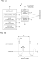
- FIG. 1A is a diagram showing a configuration of a measurement device 1.
- the measurement device 1 shown in FIG. 1A is a time-of-flight (ToF) device that measures a distance to an object in front.
- ToF time-of-flight
- an indirect ToF camera is used.
- Such a measurement device 1 can remove influence of fog or rain, and perform imaging and measurement even in bad weather.
- the measurement device 1 is provided, for example, in a vehicle.
- the measurement device 1 includes a light emitting unit 10, an imaging unit 20, and a control unit 30.
- the light emitting unit 10 emits (projects) light to a space to be imaged.
- the light emitting unit 10 controls light emission according to an instruction from the control unit 30.
- the light emitting unit 10 includes a light source 12 and a projecting optical system (not shown) that emits light generated by the light source 12.
- the light source 12 includes a light emitting element.
- the light source 12 emits pulsed laser light under the control of the control unit 30.
- this pulsed light is also referred to as a light emission pulse.
- the imaging unit 20 (indirect ToF camera) performs imaging based on exposure to light reflected by a target of distance measurement.
- the imaging unit 20 includes an imaging sensor 22 and an exposure optical system (not shown) that guides incident (exposed) light to the imaging sensor 22.
- the imaging sensor 22 images an object to be imaged according to an instruction from the control unit 30 and outputs image data obtained by imaging to an image acquisition unit 34 of the control unit 30.
- a value (pixel data) of each pixel constituting the image data indicates a signal value corresponding to an exposure amount.
- the imaging sensor 22 will be described in detail later.
- the control unit 30 controls the measurement device 1.
- the control unit 30 is implemented by a hardware configuration such as an element or a circuit, such as a memory or a CPU.
- the control unit 30 implements a predetermined function by the CPU executing a program stored in the memory.
- FIG. 1A shows various functions implemented by the control unit 30.
- the control unit 30 includes a timing control unit 32, the image acquisition unit 34, a time calculation unit 36, and a distance calculation unit 38.
- the timing control unit 32 controls a light emission timing of the light emitting unit 10 and an exposure timing of the imaging unit 20.
- the light emission timing and the exposure timing will be described later.
- the image acquisition unit 34 acquires image data from the imaging sensor 22 of the imaging unit 20.
- the image acquisition unit 34 includes a memory (not shown) that stores the acquired image data.
- the time calculation unit 36 calculates an arrival time (time of flight of light: ToF) from when the light emitting unit 10 emits light until the reflected light reaches the imaging unit 20.
- the time calculation unit 36 corresponds to a "calculation unit".
- the distance calculation unit 38 calculates a distance based on the arrival time of the light. As will be described later, a distance image can be acquired by calculating a distance for each pixel.
- FIG. 1B is a diagram showing light emission timings and exposure timings.
- FIG. 2 is a diagram showing distance image creation using the indirect ToF.
- the control unit 30 causes the light emitting unit 10 to emit a light emission pulse.
- a width of the light emission pulse (hereinafter, pulse width) is Lw.
- the control unit 30 (timing control unit 32) causes the imaging sensor 22 of the imaging unit 20 to be exposed to the reflected light after a time Tdelay from emission of the light emission pulse.
- An exposure period is set based on the delay time Tdelay and an exposure width Gw.
- the time Tdelay is a time (delay time) from the emission of the light emission pulse to a start of the exposure period.
- the delay time Tdelay is set according to a distance to a measurement target region. That is, by setting a short time from when the light emitting unit 10 emits the light emission pulse until the imaging sensor 22 starts exposure, an image of a target (object that reflects light) in a short distance region can be acquired. Conversely, by setting a long time from when the light emitting unit 10 emits the light emission pulse until the imaging sensor 22 starts exposure, an image of a target in a long distance region can be acquired.
- the exposure width Gw is a width of the exposure period (that is, a period from a start of the exposure to an end of the exposure).
- the width of the exposure period defines a length of the measurement target region in a measurement direction. Accordingly, the smaller the exposure width Gw is, the higher a distance resolution becomes.
- FIG. 2 different exposure periods are set according to the distance to the measurement target region.
- Four regions are shown in FIG. 2 for simplicity, but the number N of regions is actually greater than four.
- the light emission and the exposure are repeated a plurality of times at a cycle Tp shown in FIG. 1B .
- This is for storing charges in the imaging sensor 22 to be described later.
- a target object that reflects light
- the image for each region may be referred to as a "range image”.
- a value (image data) of each pixel constituting the image indicates a signal value corresponding to an exposure amount.
- the measurement device 1 acquires image data on a plurality of regions of different distances, and can acquire a distance image indicating a distance to a target based on a plurality of pieces of acquired image data.
- This distance image may be referred to as a "frame”.
- a multi-tap CMOS image sensor is used as the imaging sensor 22.
- the imaging sensor 22 is not limited to the multi-tap CMOS image sensor. The number of measurable regions for once light emission may be one.
- FIG. 3 is a diagram showing a configuration example of the imaging sensor 22.
- a plurality of pixels 221 are two-dimensionally arranged (for example, 640 ⁇ 480) in the imaging sensor 22.
- One light receiving element PD and a plurality of (here, four) signal reading units RU1 to RU4 corresponding to the one light receiving element PD are provided in each pixel 221.
- the signal reading units RU1 to RU4 have the same configuration (only numerals of constituent elements are different). In the following description, the signal reading unit is mainly described using the signal reading unit RU1.
- the light receiving element PD is an element (for example, a photodiode) that generates charges corresponding to an exposure amount.
- the signal reading unit RU1 includes an storage unit CS1, a transistor G1, a reset transistor RT1, a source follower transistor SF1, and a selection transistor SL1.
- the storage unit CS1 stores the charges generated by the light receiving element PD, and includes a storage capacitor C 1 and a floating diffusion FD1.
- the transistor G1 is provided between the light receiving element PD and the storage unit CS1.
- the transistor G1 is turned on in a predetermined exposure period (for example, an exposure period A to be described later) and supplies the charges generated by the light receiving element PD to the storage unit CS1 based on an instruction from the timing control unit 32 of the control unit 30.
- transistors G2 to G4 supply the charges generated by the light receiving element PD to the storage units CS2 to CS4, respectively, based on instructions from the timing control unit 32. That is, transistors G1 to G4 correspond to a "drive circuit" that distributes the charges generated by the light receiving element PD to storage units CS1 to CS4 according to the exposure period.
- the imaging sensor 22 can divide and store the charges generated in four exposure periods in the storage units (CS1 to CS4) corresponding to each exposure period.
- the charges are repeatedly stored in each storage unit according to the number n of times of repetition.
- the charges stored in each storage unit correspond to an amount of light to which the light receiving element PD is exposed in each exposure period.
- a signal value is output based on the charges stored in the storage unit.
- the signal value based on the charges stored in the storage unit is a signal value corresponding to the exposure amount in each exposure period.
- four regions can be measured by imaging once. That is, four range images are obtained by imaging once.
- the number of (here, four) range images obtained by imaging once may be referred to as a "subframe”.
- a plurality of regions (here, four regions) measured by imaging once may be referred to as a "zone”.
- FIG. 10 is a diagram showing a relationship between light emission and exposure according to a comparative example.
- a pulse width of a light emission pulse is Lw.
- Apulse width of the reflected light is also denoted by Lw.
- exposure A and exposure B are set.
- An exposure period (exposure period A) corresponding to a predetermined region A is set for the exposure A.
- a delay time of the exposure A with respect to a start (time 0) of light emission of the light emission pulse is a delay time Ta (corresponding to Tdelay in FIG. 1B ).
- the pixel 221 of the imaging sensor 22 acquires a signal value Sa corresponding to an exposure amount of the reflected light in the exposure period A having the exposure width Gw'.
- An exposure period (exposure period B) corresponding to a region B is set for the exposure B.
- the region B is a region adjacent to the region A in a measurement direction.
- the pixel 221 of the imaging sensor 22 acquires a signal value Sb corresponding to an exposure amount of the reflected light in the exposure period B.
- Tx is an arrival time (time of flight of light: ToF) from emission of light (light emission pulse) to arrival of the reflected light.
- ToF time of flight of light
- the exposure width Gw' is set to the same value as the pulse width Lw of the light emission pulse. As described above, reducing a pulse width is effective in increasing a distance resolution. However, the pulse width Lw may not be reduced due to structural and cost restrictions of the light source. Therefore, if there is a restriction that the exposure width Gw' is equal to the pulse width Lw, it is difficult to increase the distance resolution.
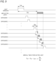
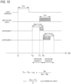
- FIG. 4 is a diagram showing a relationship between light emission and exposure in the measurement device 1 according to the present embodiment.
- a pulse width of the light emission pulse (and a pulse width of the reflected light) is Lw equal to that in the comparative example.
- exposure A, exposure B, exposure C, and exposure D are set.
- Each of widths of exposure periods (exposure widths) of exposure A to D is Gw.
- H/L levels of the exposure A to D indicate whether the transistors G1 to G4 in FIG. 3 are turned on or off.
- the transistor G1 is turned on in the exposure period A (exposure width Gw) of the exposure A, and charges generated by the light receiving element PD are stored in the storage capacitor C1 of the storage unit CS1.
- An exposure period (exposure period A) corresponding to a region A is set for the exposure A.
- a delay time of the exposure A with respect to a start (time 0) of light emission of the light emission pulse is a delay time Ta (corresponding to Tdelay in FIG. 1B ).
- the exposure width Gw is smaller than the exposure width Gw' in the comparative example. That is, an exposure period of the exposure A is set to be shorter than the pulse width Lw of the light emission pulse. By shortening the exposure period in this way, measurement accuracy can be improved as compared with the comparative example.
- the exposure width Gw of the exposure period A is set to an integer fraction of the pulse width Lw of the light emission pulse.
- the exposure width Gw is set to one third of the pulse width Lw of the light emission pulse.
- the exposure width Gw is not limited to one third of the pulse width Lw of the light emission pulse.
- the pixel 221 of the imaging sensor 22 acquires a signal value Sa corresponding to an exposure amount of the reflected light in the exposure period A having the exposure width Gw.
- the signal value Sa corresponds to a value (pixel data) of a pixel constituting image data of an image (range image) of the region A.
- FIG. 4 is shown based on charges in once exposure for description, but actually a signal value S (here, the signal value Sa) is a signal value corresponding to charges (corresponding to an exposure amount) stored by repeating the exposure for the number n of times of repetition.
- Exposure periods B to D corresponding to regions B to D are respectively set for exposure B to D.
- the region B is a region adjacent to the region A in a measurement direction
- the region C is a region adjacent to the region B in the measurement direction
- the region D is a region adjacent to the region C in the measurement direction.
- the pixel 221 of the imaging sensor 22 acquires signal values Sb to Sd corresponding to exposure amounts of the reflected light in the exposure periods B to D of the exposure B to D.
- the signal values Sb to Sd correspond to values (pixel data) of pixels constituting image data of images (range images) of the regions B to D.
- Regions A to D correspond to "three or more consecutive exposure periods that can include the pulse width", and here correspond to four exposure periods.
- the control unit 30 calculates the arrival time Tx of the reflected light based on signal values corresponding to three or more consecutive exposure periods that can include the pulse width Lw. Specifically, the control unit 30 calculates the arrival time Tx of the reflected light based on a ratio (Sx/St) of a signal value Sx corresponding to an exposure amount before a boundary timing of any two exposure periods among the three or more consecutive exposure periods that can include the pulse width Lw to a sum St of the signal values corresponding to the three or more exposure periods.
- the three or more consecutive exposure periods that can include the pulse width Lw are periods (exposure periods A to D) of the exposure A to D here.
- a reason why it is set to three or more is to ensure a period in which exposure to the reflected light having the pulse width Lw can be performed in a situation where the width (exposure width) Gw of the exposure period is set smaller than the pulse width Lw.
- the signal values corresponding to three or more consecutive exposure periods that can include the pulse width Lw are signal values Sa, Sb, Sc, and Sd.
- the boundary timing is Tb, Tc, or Td in FIG. 4 .
- the boundary timing Ts is preferably a boundary between two exposure periods that are the second and subsequent periods among the three or more exposure periods that can include the pulse width Lw.
- the boundary timing Ts is preferably Tc or Td.
- control unit 30 calculates the arrival time Tx according to the second equation (Equation (4)) or the third equation (Equation (5)) among the above three calculation equations. Accordingly, influence of the error in the signal value Sa can be reduced.
- FIG. 5 is an overall flowchart showing an operation of the measurement device 1 (mainly the control unit 30) according to the present embodiment.
- the control unit 30 executes each processing in the drawing by the CPU executing the program stored in the memory.
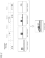
- FIG. 6 is a diagram showing image acquisition.
- FIG. 6 shows timings at which images of regions 1 to 8 among a plurality of regions 1 to N are acquired.
- a left side of an upper diagram shows timings for acquiring images of zone 1 (regions 1 to 4), and a right side thereof shows timings of acquiring images of zone 2 (regions 5 to 8).
- Regions 1 to 4 and regions 5 to 8 have different delay time of exposure timings with respect to light emission timings. Specifically, in the regions 5 to 8, the exposure timings (timings corresponding to Tdelay in FIG. 1B ) with respect to the light emission timings are later than those in the regions 1 to 4, respectively.
- a lower diagram in FIG. 6 is a diagram showing exposure timings in the regions 1 to 8 with a light emission pulse as a reference. Normally, light emission for the regions 1 to 4 and light emission for the regions 5 to 8 are separate as shown in the upper diagram in FIG. 6 , but the lower diagram shows the exposure timings in the regions 1 to 8 with a light emission timing as a reference.
- the above "three or more consecutive exposure periods that can include the pulse width Lw" are not limited to those constituted only by exposure periods (for example, exposure periods corresponding to the regions 1 to 4) having the same light emission timing, and may include exposure periods (for example, exposure periods corresponding to the regions 4 and 5) having different emission timings.
- the timing control unit 32 of the control unit 30 causes the light emitting unit 10d to emit light at the cycle Tp, and controls an exposure timing of the imaging unit 20 according to a light emission timing.
- the image acquisition unit 34 acquires an image captured by the imaging unit 20 at each exposure timing (S10).
- images of the regions 1 to 4 are acquired. That is, the imaging sensor 22 of the imaging unit 20 is exposed to light in the exposure periods A to D delayed from the light emission timing for each pixel of the image.
- the control unit 30 repeatedly performs exposure for each cycle Tp, accumulates charges in the storage units CS1 to CS4, and acquires the accumulated charges (signal values Sa to Sd). Then, image data on the acquired range images (subframes) of the regions 1 to 4 is written into an image memory of the image acquisition unit 34 (S11).
- the control unit 30 acquires images of the regions 5 to 8.
- a delay time (delay time of the exposure A to D) with respect to the light emission timing in the regions 5 to 8 is set to be longer than that in the regions 1 to 4.
- the number of times of repetition is set to increase as the measurement target region becomes further away.
- image data on range images (subframes) of the regions 5 to 8 is written into the image memory of the image acquisition unit 34.
- control unit 30 determines whether images up to the region N (images of all the regions) are acquired (S12). When the images of all the regions up to the region N are not acquired (NO in S12), the control unit 30 returns to step S10 and further acquires an image. When the images of all the regions up to the region N are acquired (YES in S12), the control unit 30 (specifically, the time calculation unit 36 and the distance calculation unit 38) executes distance calculation processing to acquire a distance image (S13).
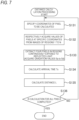
- FIG. 7 is a flowchart showing the distance calculation processing.
- FIG. 8 is a conceptual diagram showing the distance calculation processing
- FIG. 9 is a conceptual diagram showing the distance calculation processing.
- FIG. 9 is a diagram substantially equivalent to FIG. 8 .
- control unit 30 specifies coordinates of a pixel to be calculated (S131). That is, the coordinates of the pixel in two dimensions form are specified.
- control unit 30 acquires values (signal values) of pixels at specific coordinates from images of the regions 1 to N, respectively (S132). That is, as shown in FIG. 8 , the control unit 30 acquires values of pixels at the same coordinates (specific coordinates) from the images of the regions 1 to N.
- the control unit 30 extracts four pixels in regions continuously exposed to the reflected light (S133). For example, the control unit 30 extracts four pixels in regions continuously exposed to the reflected light by extracting four pixels having the highest sum of gradation values. Alternatively, the control unit 30 may extract, for example, four pixels located before and after a pixel having a maximum gradation value (value indicating a large exposure amount).
- FIG. 8 it is assumed that four pixels (pixels at the same coordinates) in the regions A to D continuously exposed to the reflected light are extracted, and gradation values thereof are Sa, Sb, Sc, and Sd, respectively.
- the extracted gradation values Sa, Sb, Sc, and Sd correspond to the "signal values corresponding to three or more consecutive exposure periods that can include the pulse width Lw".
- the time calculation unit 36 of the control unit 30 calculates the arrival time Tx using the four gradation values (Sa, Sb, Sc, Sd) according to Equation (4) or Equation (5) described above (S134).
- the distance calculation unit 38 of the control unit 30 obtains the distance L according to Equation (2) using the arrival time Tx calculated by the time calculation unit 36 and the speed Co of the light (S135).
- the control unit 30 returns to step S131 and executes the same calculation for the next pixel (pixel at other coordinates).
- the control unit 30 ends the distance calculation processing.
- the control unit 30 can acquire the distance image (frame: see FIG. 2 ) by executing the distance calculation processing on all the pixels.
- the control unit 30 After the distance calculation processing (S13), the control unit 30 writes the distance image into the memory (S14). The control unit 30 executes color conversion processing on the distance image (S15). The color conversion processing is processing of color-coding a color of each pixel according to the distance. Accordingly, it is easy to understand presence of an object and a distance to the object. Then, the control unit 30 executes display processing (S16). The display processing is processing of displaying the color-coded distance image on a display. The color conversion processing (S15) and the display processing (S16) may not be executed.
- control unit 30 When the processing is not completed (NO in S17), the control unit 30 returns to step S10 and repeats image acquisition for the regions 1 to N. When the processing is completed (YES in S17), the control unit 30 ends a measurement operation.
- the measurement device 1 includes: the light emitting unit 10 configured to emit a light emission pulse; the imaging sensor 22 configured to output a signal value corresponding to an exposure amount for each pixel 221; the timing control unit 32 configured to expose the pixel 221 of the imaging sensor 22 to reflected light in an exposure period that is set according to a measurement target region and has the exposure width Gw shorter than the pulse width Lw of the light emission pulse; and the time calculation unit 36 configured to calculate the arrival time Tx of the reflected light based on the signal values Sa to Sd corresponding to the three or more consecutive exposure periods A to D that can include the pulse width Lw. Accordingly, a distance resolution can be increased, and measurement accuracy can be improved.
- the time calculation unit 36 calculates the arrival time Tx of the reflected light based on a ratio of the signal value Sx corresponding to the exposure amount before a boundary timing (for example, Tc and Td) of any two exposure periods (for example, the exposure periods C and D) among the exposure periods A to D.
- the two exposure periods may be the exposure periods B and C, in which case the boundary timing may be Tb and Tc.
- the two exposure periods may be the exposure periods B and D, in which case the boundary timing may be Tb and Td.
- the boundary timing is preferably a timing (boundary timings Tc and Td) of a boundary between two exposure periods that are the second and subsequent exposure periods B to D among the exposure periods A to D that can include the pulse width Lw. Accordingly, influence of an error in the signal value Sa can be reduced.
- the time calculation unit 36 calculates the arrival time Tx by setting the number of consecutive exposure periods that can include the pulse width Lw to four that is larger by one than three that is an integer part of Lw/Gw. Accordingly, the minimum number of exposure periods can be set.
- the timing control unit 32 sets the width Gw of the exposure period to an integer fraction (one third in the present embodiment) of the pulse width Lw of the light emission pulse. Accordingly, the measurement accuracy can be improved.
- the imaging sensor 22 includes the light receiving element PD that generates charges corresponding to the exposure amount for each pixel 221, four storage units CS 1 to CS4 that accumulate the charges, and a drive circuit (transistors G1 to G4) that distributes and accumulates the charges to the respective storage units CS1 to CS4 according to the exposure periods A to D, and distributes and accumulates charges generated by one light emission pulse to the respective storage units CS1 to CS4 according to the exposure periods A to D. Accordingly, a plurality of exposure periods can be set for once light emission, and a plurality of regions can be measured for once light emission.
Landscapes
- Engineering & Computer Science (AREA)
- Physics & Mathematics (AREA)
- Computer Networks & Wireless Communication (AREA)
- General Physics & Mathematics (AREA)
- Radar, Positioning & Navigation (AREA)
- Remote Sensing (AREA)
- Electromagnetism (AREA)
- Optical Radar Systems And Details Thereof (AREA)
Applications Claiming Priority (2)
| Application Number | Priority Date | Filing Date | Title |
|---|---|---|---|
| JP2021211069 | 2021-12-24 | ||
| PCT/JP2022/043362 WO2023120012A1 (ja) | 2021-12-24 | 2022-11-24 | 測定装置 |
Publications (2)
| Publication Number | Publication Date |
|---|---|
| EP4455731A1 true EP4455731A1 (de) | 2024-10-30 |
| EP4455731A4 EP4455731A4 (de) | 2025-03-26 |
Family
ID=86902252
Family Applications (1)
| Application Number | Title | Priority Date | Filing Date |
|---|---|---|---|
| EP22910730.5A Pending EP4455731A4 (de) | 2021-12-24 | 2022-11-24 | Messvorrichtung |
Country Status (5)
| Country | Link |
|---|---|
| US (1) | US20250052902A1 (de) |
| EP (1) | EP4455731A4 (de) |
| JP (1) | JPWO2023120012A1 (de) |
| CN (1) | CN118451343A (de) |
| WO (1) | WO2023120012A1 (de) |
Family Cites Families (7)
| Publication number | Priority date | Publication date | Assignee | Title |
|---|---|---|---|---|
| JP2001337166A (ja) * | 2000-05-26 | 2001-12-07 | Minolta Co Ltd | 3次元入力方法および3次元入力装置 |
| JP5675468B2 (ja) * | 2011-03-31 | 2015-02-25 | 本田技研工業株式会社 | 測距システム |
| DE102014013099B4 (de) * | 2014-09-03 | 2019-11-14 | Basler Aktiengesellschaft | Verfahren und Vorrichtung zur vereinfachten Erfassung eines Tiefenbildes |
| JP6539990B2 (ja) * | 2014-11-14 | 2019-07-10 | 株式会社デンソー | 光飛行型測距装置 |
| EP3864432A4 (de) * | 2018-11-20 | 2022-06-29 | Sense Photonics, Inc. | Verfahren und systeme zum räumlich verteilten strobing |
| JP7463671B2 (ja) | 2019-08-01 | 2024-04-09 | Toppanホールディングス株式会社 | 距離画像撮像装置、及び距離画像撮像方法 |
| WO2021201269A1 (ja) * | 2020-04-02 | 2021-10-07 | 株式会社小糸製作所 | ゲーティングカメラ、車両用センシングシステム、車両用灯具 |
-
2022
- 2022-11-24 US US18/722,939 patent/US20250052902A1/en active Pending
- 2022-11-24 WO PCT/JP2022/043362 patent/WO2023120012A1/ja not_active Ceased
- 2022-11-24 CN CN202280085641.4A patent/CN118451343A/zh active Pending
- 2022-11-24 JP JP2023569193A patent/JPWO2023120012A1/ja active Pending
- 2022-11-24 EP EP22910730.5A patent/EP4455731A4/de active Pending
Also Published As
| Publication number | Publication date |
|---|---|
| JPWO2023120012A1 (de) | 2023-06-29 |
| US20250052902A1 (en) | 2025-02-13 |
| EP4455731A4 (de) | 2025-03-26 |
| WO2023120012A1 (ja) | 2023-06-29 |
| CN118451343A (zh) | 2024-08-06 |
Similar Documents
| Publication | Publication Date | Title |
|---|---|---|
| US11769775B2 (en) | Distance-measuring imaging device, distance measuring method of distance-measuring imaging device, and solid-state imaging device | |
| US11448757B2 (en) | Distance measuring device | |
| CN114175618B (zh) | 距离图像摄像装置以及距离图像摄像方法 | |
| US10764518B2 (en) | Pixel structure | |
| US9787912B2 (en) | Image capture device | |
| EP3361283B1 (de) | Bildgebungsvorrichtung und festkörperbildelement dafür | |
| EP3425901A1 (de) | Bildgebungsvorrichtung und festkörperbildgebungselement dafür | |
| EP3015882B1 (de) | Entfernungsmessvorrichtung | |
| EP3379291A1 (de) | Bildgebungsvorrichtung und festkörperbildgebungselement dafür | |
| JP3574607B2 (ja) | 3次元画像入力装置 | |
| JP7339290B2 (ja) | 撮像装置及び距離情報算出方法 | |
| US20220003876A1 (en) | Distance image obtaining method and distance detection device | |
| EP4455731A1 (de) | Messvorrichtung | |
| US20220244394A1 (en) | Movement amount estimation device, movement amount estimation method, movement amount estimation program, and movement amount estimation system | |
| US20230078063A1 (en) | Distance measurement device and distance measurement system | |
| US20250123374A1 (en) | Measurement device | |
| EP4468031A1 (de) | Messvorrichtung | |
| US20230204727A1 (en) | Distance measurement device and distance measurement method | |
| EP4468035A1 (de) | Messvorrichtung | |
| EP4492811A1 (de) | Photoelektrische wandlerschaltung und photoelektrische wandlervorrichtung | |
| US11768277B2 (en) | Time-of-flight sensor and control method thereof | |
| US20230019246A1 (en) | Time-of-flight imaging circuitry, time-of-flight imaging system, and time-of-flight imaging method | |
| CN114600150B (zh) | 图像处理装置、图像处理方法、图像处理程序以及图像处理系统 | |
| US20230213627A1 (en) | A method and active pixel array for a time of flight detection | |
| WO2023166988A1 (ja) | 測定装置 |
Legal Events
| Date | Code | Title | Description |
|---|---|---|---|
| STAA | Information on the status of an ep patent application or granted ep patent |
Free format text: STATUS: THE INTERNATIONAL PUBLICATION HAS BEEN MADE |
|
| PUAI | Public reference made under article 153(3) epc to a published international application that has entered the european phase |
Free format text: ORIGINAL CODE: 0009012 |
|
| STAA | Information on the status of an ep patent application or granted ep patent |
Free format text: STATUS: REQUEST FOR EXAMINATION WAS MADE |
|
| 17P | Request for examination filed |
Effective date: 20240624 |
|
| AK | Designated contracting states |
Kind code of ref document: A1 Designated state(s): AL AT BE BG CH CY CZ DE DK EE ES FI FR GB GR HR HU IE IS IT LI LT LU LV MC ME MK MT NL NO PL PT RO RS SE SI SK SM TR |
|
| REG | Reference to a national code |
Ref country code: DE Ref legal event code: R079 Free format text: PREVIOUS MAIN CLASS: G01S0017894000 Ipc: G01S0017180000 |
|
| A4 | Supplementary search report drawn up and despatched |
Effective date: 20250220 |
|
| RIC1 | Information provided on ipc code assigned before grant |
Ipc: G01S 7/4865 20200101ALI20250214BHEP Ipc: G01S 7/4863 20200101ALI20250214BHEP Ipc: G01S 17/894 20200101ALI20250214BHEP Ipc: G01S 17/18 20200101AFI20250214BHEP |
|
| DAV | Request for validation of the european patent (deleted) | ||
| DAX | Request for extension of the european patent (deleted) |