EP4454792A1 - Outil de coupe - Google Patents
Outil de coupe Download PDFInfo
- Publication number
- EP4454792A1 EP4454792A1 EP22957355.5A EP22957355A EP4454792A1 EP 4454792 A1 EP4454792 A1 EP 4454792A1 EP 22957355 A EP22957355 A EP 22957355A EP 4454792 A1 EP4454792 A1 EP 4454792A1
- Authority
- EP
- European Patent Office
- Prior art keywords
- layer
- tisicn
- balance
- cutting
- cutting tool
- Prior art date
- Legal status (The legal status is an assumption and is not a legal conclusion. Google has not performed a legal analysis and makes no representation as to the accuracy of the status listed.)
- Pending
Links
Images


Classifications
-
- B—PERFORMING OPERATIONS; TRANSPORTING
- B23—MACHINE TOOLS; METAL-WORKING NOT OTHERWISE PROVIDED FOR
- B23B—TURNING; BORING
- B23B27/00—Tools for turning or boring machines; Tools of a similar kind in general; Accessories therefor
- B23B27/14—Cutting tools of which the bits or tips or cutting inserts are of special material
- B23B27/16—Cutting tools of which the bits or tips or cutting inserts are of special material with exchangeable cutting bits or cutting inserts, e.g. able to be clamped
- B23B27/1603—Cutting tools of which the bits or tips or cutting inserts are of special material with exchangeable cutting bits or cutting inserts, e.g. able to be clamped with specially shaped plate-like exchangeable cutting inserts, e.g. chip-breaking groove
- B23B27/1611—Cutting tools of which the bits or tips or cutting inserts are of special material with exchangeable cutting bits or cutting inserts, e.g. able to be clamped with specially shaped plate-like exchangeable cutting inserts, e.g. chip-breaking groove characterised by having a special shape
-
- C—CHEMISTRY; METALLURGY
- C23—COATING METALLIC MATERIAL; COATING MATERIAL WITH METALLIC MATERIAL; CHEMICAL SURFACE TREATMENT; DIFFUSION TREATMENT OF METALLIC MATERIAL; COATING BY VACUUM EVAPORATION, BY SPUTTERING, BY ION IMPLANTATION OR BY CHEMICAL VAPOUR DEPOSITION, IN GENERAL; INHIBITING CORROSION OF METALLIC MATERIAL OR INCRUSTATION IN GENERAL
- C23C—COATING METALLIC MATERIAL; COATING MATERIAL WITH METALLIC MATERIAL; SURFACE TREATMENT OF METALLIC MATERIAL BY DIFFUSION INTO THE SURFACE, BY CHEMICAL CONVERSION OR SUBSTITUTION; COATING BY VACUUM EVAPORATION, BY SPUTTERING, BY ION IMPLANTATION OR BY CHEMICAL VAPOUR DEPOSITION, IN GENERAL
- C23C16/00—Chemical coating by decomposition of gaseous compounds, without leaving reaction products of surface material in the coating, i.e. chemical vapour deposition [CVD] processes
- C23C16/22—Chemical coating by decomposition of gaseous compounds, without leaving reaction products of surface material in the coating, i.e. chemical vapour deposition [CVD] processes characterised by the deposition of inorganic material, other than metallic material
- C23C16/30—Deposition of compounds, mixtures or solid solutions, e.g. borides, carbides, nitrides
- C23C16/36—Carbonitrides
-
- B—PERFORMING OPERATIONS; TRANSPORTING
- B23—MACHINE TOOLS; METAL-WORKING NOT OTHERWISE PROVIDED FOR
- B23B—TURNING; BORING
- B23B27/00—Tools for turning or boring machines; Tools of a similar kind in general; Accessories therefor
- B23B27/14—Cutting tools of which the bits or tips or cutting inserts are of special material
-
- C—CHEMISTRY; METALLURGY
- C23—COATING METALLIC MATERIAL; COATING MATERIAL WITH METALLIC MATERIAL; CHEMICAL SURFACE TREATMENT; DIFFUSION TREATMENT OF METALLIC MATERIAL; COATING BY VACUUM EVAPORATION, BY SPUTTERING, BY ION IMPLANTATION OR BY CHEMICAL VAPOUR DEPOSITION, IN GENERAL; INHIBITING CORROSION OF METALLIC MATERIAL OR INCRUSTATION IN GENERAL
- C23C—COATING METALLIC MATERIAL; COATING MATERIAL WITH METALLIC MATERIAL; SURFACE TREATMENT OF METALLIC MATERIAL BY DIFFUSION INTO THE SURFACE, BY CHEMICAL CONVERSION OR SUBSTITUTION; COATING BY VACUUM EVAPORATION, BY SPUTTERING, BY ION IMPLANTATION OR BY CHEMICAL VAPOUR DEPOSITION, IN GENERAL
- C23C16/00—Chemical coating by decomposition of gaseous compounds, without leaving reaction products of surface material in the coating, i.e. chemical vapour deposition [CVD] processes
- C23C16/44—Chemical coating by decomposition of gaseous compounds, without leaving reaction products of surface material in the coating, i.e. chemical vapour deposition [CVD] processes characterised by the method of coating
- C23C16/455—Chemical coating by decomposition of gaseous compounds, without leaving reaction products of surface material in the coating, i.e. chemical vapour deposition [CVD] processes characterised by the method of coating characterised by the method used for introducing gases into reaction chamber or for modifying gas flows in reaction chamber
- C23C16/45563—Gas nozzles
- C23C16/45574—Nozzles for more than one gas
-
- C—CHEMISTRY; METALLURGY
- C23—COATING METALLIC MATERIAL; COATING MATERIAL WITH METALLIC MATERIAL; CHEMICAL SURFACE TREATMENT; DIFFUSION TREATMENT OF METALLIC MATERIAL; COATING BY VACUUM EVAPORATION, BY SPUTTERING, BY ION IMPLANTATION OR BY CHEMICAL VAPOUR DEPOSITION, IN GENERAL; INHIBITING CORROSION OF METALLIC MATERIAL OR INCRUSTATION IN GENERAL
- C23C—COATING METALLIC MATERIAL; COATING MATERIAL WITH METALLIC MATERIAL; SURFACE TREATMENT OF METALLIC MATERIAL BY DIFFUSION INTO THE SURFACE, BY CHEMICAL CONVERSION OR SUBSTITUTION; COATING BY VACUUM EVAPORATION, BY SPUTTERING, BY ION IMPLANTATION OR BY CHEMICAL VAPOUR DEPOSITION, IN GENERAL
- C23C16/00—Chemical coating by decomposition of gaseous compounds, without leaving reaction products of surface material in the coating, i.e. chemical vapour deposition [CVD] processes
- C23C16/44—Chemical coating by decomposition of gaseous compounds, without leaving reaction products of surface material in the coating, i.e. chemical vapour deposition [CVD] processes characterised by the method of coating
- C23C16/455—Chemical coating by decomposition of gaseous compounds, without leaving reaction products of surface material in the coating, i.e. chemical vapour deposition [CVD] processes characterised by the method of coating characterised by the method used for introducing gases into reaction chamber or for modifying gas flows in reaction chamber
- C23C16/45563—Gas nozzles
- C23C16/45578—Elongated nozzles, tubes with holes
-
- C—CHEMISTRY; METALLURGY
- C23—COATING METALLIC MATERIAL; COATING MATERIAL WITH METALLIC MATERIAL; CHEMICAL SURFACE TREATMENT; DIFFUSION TREATMENT OF METALLIC MATERIAL; COATING BY VACUUM EVAPORATION, BY SPUTTERING, BY ION IMPLANTATION OR BY CHEMICAL VAPOUR DEPOSITION, IN GENERAL; INHIBITING CORROSION OF METALLIC MATERIAL OR INCRUSTATION IN GENERAL
- C23C—COATING METALLIC MATERIAL; COATING MATERIAL WITH METALLIC MATERIAL; SURFACE TREATMENT OF METALLIC MATERIAL BY DIFFUSION INTO THE SURFACE, BY CHEMICAL CONVERSION OR SUBSTITUTION; COATING BY VACUUM EVAPORATION, BY SPUTTERING, BY ION IMPLANTATION OR BY CHEMICAL VAPOUR DEPOSITION, IN GENERAL
- C23C28/00—Coating for obtaining at least two superposed coatings either by methods not provided for in a single one of groups C23C2/00 - C23C26/00 or by combinations of methods provided for in subclasses C23C and C25C or C25D
- C23C28/04—Coating for obtaining at least two superposed coatings either by methods not provided for in a single one of groups C23C2/00 - C23C26/00 or by combinations of methods provided for in subclasses C23C and C25C or C25D only coatings of inorganic non-metallic material
- C23C28/042—Coating for obtaining at least two superposed coatings either by methods not provided for in a single one of groups C23C2/00 - C23C26/00 or by combinations of methods provided for in subclasses C23C and C25C or C25D only coatings of inorganic non-metallic material including a refractory ceramic layer, e.g. refractory metal oxides, ZrO2, rare earth oxides
-
- C—CHEMISTRY; METALLURGY
- C23—COATING METALLIC MATERIAL; COATING MATERIAL WITH METALLIC MATERIAL; CHEMICAL SURFACE TREATMENT; DIFFUSION TREATMENT OF METALLIC MATERIAL; COATING BY VACUUM EVAPORATION, BY SPUTTERING, BY ION IMPLANTATION OR BY CHEMICAL VAPOUR DEPOSITION, IN GENERAL; INHIBITING CORROSION OF METALLIC MATERIAL OR INCRUSTATION IN GENERAL
- C23C—COATING METALLIC MATERIAL; COATING MATERIAL WITH METALLIC MATERIAL; SURFACE TREATMENT OF METALLIC MATERIAL BY DIFFUSION INTO THE SURFACE, BY CHEMICAL CONVERSION OR SUBSTITUTION; COATING BY VACUUM EVAPORATION, BY SPUTTERING, BY ION IMPLANTATION OR BY CHEMICAL VAPOUR DEPOSITION, IN GENERAL
- C23C28/00—Coating for obtaining at least two superposed coatings either by methods not provided for in a single one of groups C23C2/00 - C23C26/00 or by combinations of methods provided for in subclasses C23C and C25C or C25D
- C23C28/04—Coating for obtaining at least two superposed coatings either by methods not provided for in a single one of groups C23C2/00 - C23C26/00 or by combinations of methods provided for in subclasses C23C and C25C or C25D only coatings of inorganic non-metallic material
- C23C28/044—Coating for obtaining at least two superposed coatings either by methods not provided for in a single one of groups C23C2/00 - C23C26/00 or by combinations of methods provided for in subclasses C23C and C25C or C25D only coatings of inorganic non-metallic material coatings specially adapted for cutting tools or wear applications
-
- C—CHEMISTRY; METALLURGY
- C23—COATING METALLIC MATERIAL; COATING MATERIAL WITH METALLIC MATERIAL; CHEMICAL SURFACE TREATMENT; DIFFUSION TREATMENT OF METALLIC MATERIAL; COATING BY VACUUM EVAPORATION, BY SPUTTERING, BY ION IMPLANTATION OR BY CHEMICAL VAPOUR DEPOSITION, IN GENERAL; INHIBITING CORROSION OF METALLIC MATERIAL OR INCRUSTATION IN GENERAL
- C23C—COATING METALLIC MATERIAL; COATING MATERIAL WITH METALLIC MATERIAL; SURFACE TREATMENT OF METALLIC MATERIAL BY DIFFUSION INTO THE SURFACE, BY CHEMICAL CONVERSION OR SUBSTITUTION; COATING BY VACUUM EVAPORATION, BY SPUTTERING, BY ION IMPLANTATION OR BY CHEMICAL VAPOUR DEPOSITION, IN GENERAL
- C23C30/00—Coating with metallic material characterised only by the composition of the metallic material, i.e. not characterised by the coating process
- C23C30/005—Coating with metallic material characterised only by the composition of the metallic material, i.e. not characterised by the coating process on hard metal substrates
-
- E—FIXED CONSTRUCTIONS
- E21—EARTH OR ROCK DRILLING; MINING
- E21B—EARTH OR ROCK DRILLING; OBTAINING OIL, GAS, WATER, SOLUBLE OR MELTABLE MATERIALS OR A SLURRY OF MINERALS FROM WELLS
- E21B10/00—Drill bits
- E21B10/46—Drill bits characterised by wear resisting parts, e.g. diamond inserts
-
- B—PERFORMING OPERATIONS; TRANSPORTING
- B23—MACHINE TOOLS; METAL-WORKING NOT OTHERWISE PROVIDED FOR
- B23B—TURNING; BORING
- B23B2200/00—Details of cutting inserts
- B23B2200/08—Rake or top surfaces
-
- B—PERFORMING OPERATIONS; TRANSPORTING
- B23—MACHINE TOOLS; METAL-WORKING NOT OTHERWISE PROVIDED FOR
- B23B—TURNING; BORING
- B23B2200/00—Details of cutting inserts
- B23B2200/24—Cross section of the cutting edge
- B23B2200/242—Cross section of the cutting edge bevelled or chamfered
-
- B—PERFORMING OPERATIONS; TRANSPORTING
- B23—MACHINE TOOLS; METAL-WORKING NOT OTHERWISE PROVIDED FOR
- B23B—TURNING; BORING
- B23B2200/00—Details of cutting inserts
- B23B2200/24—Cross section of the cutting edge
- B23B2200/245—Cross section of the cutting edge rounded
-
- B—PERFORMING OPERATIONS; TRANSPORTING
- B23—MACHINE TOOLS; METAL-WORKING NOT OTHERWISE PROVIDED FOR
- B23B—TURNING; BORING
- B23B2200/00—Details of cutting inserts
- B23B2200/36—Other features of cutting inserts not covered by B23B2200/04 - B23B2200/32
- B23B2200/3645—Lands, i.e. the outer peripheral section of the rake face
-
- B—PERFORMING OPERATIONS; TRANSPORTING
- B23—MACHINE TOOLS; METAL-WORKING NOT OTHERWISE PROVIDED FOR
- B23B—TURNING; BORING
- B23B2224/00—Materials of tools or workpieces composed of a compound including a metal
- B23B2224/36—Titanium nitride
-
- B—PERFORMING OPERATIONS; TRANSPORTING
- B23—MACHINE TOOLS; METAL-WORKING NOT OTHERWISE PROVIDED FOR
- B23B—TURNING; BORING
- B23B2228/00—Properties of materials of tools or workpieces, materials of tools or workpieces applied in a specific manner
- B23B2228/10—Coatings
- B23B2228/105—Coatings with specified thickness
-
- B—PERFORMING OPERATIONS; TRANSPORTING
- B23—MACHINE TOOLS; METAL-WORKING NOT OTHERWISE PROVIDED FOR
- B23B—TURNING; BORING
- B23B27/00—Tools for turning or boring machines; Tools of a similar kind in general; Accessories therefor
- B23B27/14—Cutting tools of which the bits or tips or cutting inserts are of special material
- B23B27/148—Composition of the cutting inserts
Definitions
- the present disclosure relates to a cutting tool.
- a cutting tool including a substrate and a coating film disposed on the substrate has been conventionally used for cutting process (PTL 1, PTL 2, and NPL 1).
- NPL 1 Shinya Imamura et al., "Properties and cutting performance of AlTiCrN/TiSiCN bilayer coatings deposited by cathodic-arc ion plating", Surface and Coatings Technology, 202, (2007), 820-825
- a cutting tool of the present disclosure is a cutting tool comprising a substrate and a coating film disposed on the substrate, wherein the cutting tool comprises:
- a cutting tool having a long tool lifetime can be provided.
- a description of a form "A to B" herein means an upper and lower limits of a range (that is, A or more and B or less).
- a has no description of a unit and only B has a description of a unit the unit of A and the unit of B are same.
- any conventionally known atomic ratios are included unless the atomic ratio is particularly limited, and should not be necessarily limited to an atomic ratio within a stoichiometric range.
- a ratio of numbers of atoms that constitute TiN includes any conventionally known atomic ratios.
- An embodiment of the present disclosure (hereinafter, also referred to as “the present embodiment") is a cutting tool 1 comprising a substrate 2 and a coating film 3 disposed on substrate 2, wherein cutting tool 1 comprises:
- cutting tool 1 having a long tool lifetime can be provided. It is presumed that the reason is as follows.
- the Xr and the Xe each represent 0.010 or more and 0.100 or less, and satisfy a relationship of Xr - Xe ⁇ 0.003.
- Xr and Xe are within the range of 0.10 or less, larger values of Xr and Xe (in other word, higher Si concentrations) tend to increase hardness with nanoindentation and improve the "wearing resistance". Meanwhile, the "breakage resistance” tends to easily decrease due to deterioration in toughness. In the intermittent turning of steel in particular, since cracking of the region of cutting edge 13 easily occurs due to mechanical impact, high toughness ("breakage resistance”) in the region of cutting edge 13 is required.
- TiSiCN layer 30 can entirely has an appropriate hardness, and can have excellent "wearing resistance".
- a Si concentration in the region of cutting edge 13 can be relatively reduced, and in particular, the region of cutting edge 13 can have high toughness ("breakage resistance").
- both of the excellent “wearing resistance” and the excellent “breakage resistance” can be imparted to the cutting tool, and thereby in the intermittent turning of steel in particular, a cutting tool having a long tool lifetime can be provided.
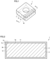
- cutting tool 1 of the present disclosure has surfaces including an upper face, a lower face, and four side faces, and cutting tool 1 has a quadrangular prism shape that is slightly short in the vertical direction as an entirety.
- cutting tool 1 a through hole that penetrates the upper and lower faces is formed.
- the adjacent side faces are connected to each other with an arc face.
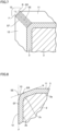
- the boundary part between rake face 11 and flank face 12, that is the region of cutting edge 13, means "a combined part of: a ridgeline E that constitutes the boundary between rake face 11 and flank face 12; and a part proximity to ridgeline E in rake face 11 and flank face 12".
- the part proximity to ridgeline E in rake face 11 and flank face 12" is determined by a shape of cutting edge 13 of cutting tool 1.
- cutting tool 1 is a tool that has a sharp-edge shape
- a negative-land-processed tool that has a negative-land-processed shape will be described.
- Fig. 2 and Fig. 3 illustrate cutting tool 1 that has a sharp-edge shape.
- "the part proximity to ridgeline E in rake face 11 and flank face 12" is defined as a region within a distance (linear distance) D from ridgeline E of 50 ⁇ m or less (the dot-hatched region in Fig. 3 ). Therefore, the region of cutting edge 13 in cutting tool 1 that has a sharp-edge shape is a part corresponding to the dot-hatched region in Fig. 3 .
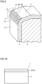
- Fig. 4 and Fig. 5 illustrate hone-processed cutting tool 1 that has a honed shape.
- Fig. 4 and Fig. 5 illustrate, in addition to each of the parts of cutting tool 1, an imaginary plane R that includes rake face 11, an imaginary plane F that includes flank face 12, an imaginary ridgeline EE formed by crossing imaginary plane Rand imaginary plane F, an imaginary boundary line ER to be a boundary of deviation between rake face 11 and imaginary plane R, and an imaginary boundary line EF to be a boundary of deviation between flank face 12 and imaginary plane F.
- "ridgeline E" is replaced for "imaginary ridgeline EE".
- the part proximity to imaginary ridgeline EE in rake face 11 and flank face 12 is defined as a region sandwiched by imaginary boundary line ER and imaginary boundary line EF (the dot-hatched region in Fig. 5 ). Therefore, the region of cutting edge 13 in cutting tool 1 that has a honed shape is a part corresponding to the dot-hatched region in Fig. 5 .
- Fig. 6 and Fig. 7 illustrate negative-land-processed cutting tool 1 that has a negative-land shape.
- Fig. 6 and Fig. 7 also illustrate, in addition to each of the parts of cutting tool 1, imaginary plane R that includes rake face 11, imaginary plane F that includes flank face 12, imaginary ridgeline EE formed by crossing imaginary plane R and imaginary plane F, imaginary boundary line ER to be a boundary of deviation between rake face 11 and imaginary plane R, and imaginary boundary line EF to be a boundary of deviation between flank face 12 and imaginary plane F.
- "ridgeline E" is also replaced for "imaginary ridgeline EE".
- the part proximity to imaginary ridgeline EE in rake face 11 and flank face 12 is defined as a region sandwiched by imaginary boundary line ER and imaginary boundary line EF (the dot-hatched region in Fig. 7 ). Therefore, the region of cutting edge 13 in cutting tool 1 that has a negative-land shape is a part corresponding to the dot-hatched region in Fig. 7 .
- Fig. 8 and Fig. 9 illustrate cutting tool 1 that has combination of a honed shape and a negative-land-processed shape.
- Fig. 8 and Fig. 9 also illustrate, in addition to each of the parts of cutting tool 1, imaginary plane R that includes rake face 11, imaginary plane F that includes flank face 12, imaginary ridgeline EE formed by crossing imaginary plane R and imaginary plane F, imaginary boundary line ER to be a boundary of deviation between rake face 11 and imaginary plane R, and imaginary boundary line EF to be a boundary of deviation between flank face 12 and imaginary plane F.
- "ridgeline E" is also replaced for "imaginary ridgeline EE".
- Imaginary plane R is a plane that includes a plane near the region of cutting edge 13 in rake face 11.
- Fig. 1 illustrates cutting tool 1 as an indexable cutting insert for turning.
- cutting tool 1 is not limited thereto, and examples thereof include a drill, an endmill, an indexable cutting insert for a drill, an indexable cutting insert for an endmill, an indexable cutting insert for milling, a metal saw, a gear-cutting tool, a reamer, and a tap.
- TiSiCN layer 30 of the present embodiment has a first TiSiCN layer positioned in rake face 11 and a second TiSiCN layer positioned in the region of cutting edge 13. That is, there are a region composed of the first TiSiCN layer and a region composed of the second TiSiCN layer in one TiSiCN layer 30.
- the composition of the first TiSiCN layer is Ti (1-Xr )Si Xr CN
- the composition of the second TiSiCN layer is Ti (1-Xe) Si Xe CN.
- the Xr and the Xe each represent 0.010 or more and 0.100 or less, and satisfy a relationship of Xr - Xe ⁇ 0.003. According to this, excellent "wearing resistance” and excellent “breakage resistance” can be imparted to the cutting tool.
- a lower limit of the Xr is preferably 0.013 or more, more preferably 0.017 or more, and further preferably 0.020 or more, from the viewpoint of improvement of the wearing resistance of rake face 11.
- An upper limit of the Xr is preferably 0.100 or less, more preferably 0.090 or less, and further preferably 0.080 or less, from the viewpoint of inhibition of deterioration in toughness (breakage resistance) of rake face 11 with the improvement of the wearing resistance of rake face 11.
- the Xr is preferably 0.013 or more and 0.100 or less, preferably 0.017 or more and 0.090 or less, and further preferably 0.020 or more and 0.080 or less.
- a lower limit of the Xe is preferably 0.010 or more, more preferably 0.015 or more, and further preferably 0.020 or more, from the viewpoint of improvement of the wearing resistance of the region of cutting edge 13.
- An upper limit of the Xe is preferably 0.097 or less, more preferably 0.090 or less, and further preferably 0.080 or less, from the viewpoint of inhibition of deterioration in toughness (breakage resistance) of the region of cutting edge 13 with the improvement of the wearing resistance of the region of cutting edge 13.
- the Xe is preferably 0.010 or more and 0.097 or less, preferably 0.015 or more and 0.090 or less, and further preferably 0.020 or more and 0.080 or less.
- a lower limit of "Xr - Xe” is preferably 0.003 or more, more preferably 0.008 or more, and further preferably 0.015 or more, particularly from the viewpoint of improvement of the wearing resistance of rake face 11 and particularly improvement of the breakage resistance of the region of cutting edge 13.
- An upper limit of "Xr - Xe” is preferably 0.100 or less, more preferably 0.090 or less, and further preferably 0.080 or less, from the viewpoint of inhibition of deterioration in toughness due to occurrence of stress concentration in the film caused by too high concentration gradient.
- "Xr - Xe” is preferably 0.003 or more and 0.100 or less, more preferably 0.008 or more and 0.090 or less, and further preferably 0.015 or more and 0.080 or less.
- the Xr and the Xe can be determined by point analysis using a scanning electron microscope equipped with energy dispersive X-ray spectrometer (SEM-EDS). The specific method will be described below.
- Cutting tool 1 is cut so that a cross section along the thickness direction of coating film 3 is exposed to obtain a measurement specimen.
- the cutting position is preferably decided with considering an actual using situation of the cutting tool.
- Fig. 11 and Fig. 12 are views for describing the cutting position of cutting tool 1.
- cutting tool 1 is used for cutting a workpiece with cutting edge 13 of the corner part (part of the apex angle that draws an arc)
- cutting tool 1 is cut so that the cutting position includes a line L1 that bisects the corner part and so that the cross section along the thickness direction of coating film 3 is exposed, as illustrated in Fig. 11 .
- cutting tool 1 is used for cutting a workpiece with cutting edge 13 of a straight part (part that draws a straight line)
- cutting tool 1 is cut so that the cutting position includes a line L2 perpendicular to cutting edge 13 of the straight part and so that the cross section along the thickness direction of coating film 3 is exposed, as illustrated in Fig. 12 .
- the exposed sectional face is polish-treated to smooth the cutting face.
- the cutting face is observed by using the SEM-EDS with 5000 times magnification, and set are three measurement fields that have rectangular shapes with 1 ⁇ m or more in the thickness direction of coating film 3 ⁇ 5 ⁇ m or more in the direction perpendicular to the thickness direction so as to include the first TiSiCN layer positioned in rake face 11 or the second TiSiCN layer positioned in the region of cutting edge 13.
- a thickness direction of the measurement field is set so as to entirely include the thickness of the first TiSiCN layer or the thickness of the second TiSiCN layer.
- the measurement field is set so as to include the first TiSiCN layer positioned in rake face 11
- the measurement field is set so as to include the first TiSiCN layer on a side of rake face 11 with a distance from ridgeline E or imaginary ridgeline EE of 200 ⁇ m or more and 500 ⁇ m or less.
- the measurement field is set so as to include the second TiSiCN layer position in the region of cutting edge 13
- the measurement field is set so as to include the second TiSiCN layer on a side of the region of cutting edge 13 with a distance from ridgeline E or imaginary ridgeline EE of 200 ⁇ m or more and 500 ⁇ m or less.
- the above three measurement fields are set so that sides of the thickness direction of each measurement field (direction illustrated by the arrow T in Fig. 13 ) are contacted with each other to continue for each measurement field.
- a part of each measurement field may be overlapped (the overlapped part is illustrated with slanted lines in Fig. 13 ).
- the measurement field is set so that a length of the overlapped part of sides in the direction perpendicular to the thickness direction of each measurement field (direction illustrated by the arrow H in Fig. 13 ) is 2 ⁇ m or less.
- the region of the first TiSiCN layer is specified. Specifically, elemental mapping by SEM-EDS is performed in each measurement field to specify a layer that contains Ti and Si. The specified layer corresponds to the first TiSiCN layer. Then, each of the above three measurement fields is observed with 5000 times magnification, and a composition ratio of Ti and Si in the first TiSiCN layer is analyzed to calculate Xr, which is the proportion of Si to the total number of atoms of Ti and Si. An average value of Xr of the three measurement fields corresponds to Xr in Ti (1-Xr )Si Xr CN, the composition of the first TiSiCN layer of the present embodiment.
- the composition of the second TiSiCN layer positioned in the cutting edge region is also measured by the same method as of the Xr except that the positions of the measurement fields are set in the second TiSiCN layer positioned in the region of cutting edge 13.
- the measurement fields are set in the second TiSiCN layer with a distance from ridgeline E or imaginary ridgeline EE of 20 ⁇ m or less.
- the SEM-EDS analysis is performed by using, for example, a scanning electron microscope (S-3400N model, manufactured by Hitachi High-Tech Corporation), and the measurement can be performed under the following conditions.
- a ratio A:B between A, which is a total of a number of Ti atoms and a number of Si atoms, and B, which is a total of a number of C atoms and a number of N atoms, is not limited to 1:1, and may be other than 1: 1 as long as the effect of the present disclosure is not impaired.
- the B can be determined by the same method as of Xr except that, in the (C1), "a composition ratio of Ti, Si, C, and N in the first TiSiCN layer is analyzed to calculate a rate of the total number of atoms of C and N to the total number of atoms of Ti, Si, C, and N.
- the number of C atoms and the number of N atoms can be determined by measurement using TEM-EDS. An average value of the rates of the three measurement fields corresponds to the B in Ti (1-Xr )Si Xr CN, the composition of the first TiSiCN layer of the present embodiment.”
- a ratio A:B between A, which is a total of a number of Ti atoms and a number of Si atoms, and B, which is a total of a number of C atoms and a number of N atoms, is not limited to 1:1, and may be other than 1: 1 as long as the effect of the present disclosure is not impaired.
- the B can be determined by the same method as the measurement method of B in the first TiSiCN layer except that "the second TiSiCN layer" is analyzed.
- the thickness of TiSiCN layer 30 is preferably 2.0 ⁇ m or more and 15 ⁇ m or less. If the thickness of TiSiCN layer 30 is less than 2.0 ⁇ m, the effect of improving the wearing resistance and the breakage resistance with TiSiCN layer 30 is hardly obtained to tend to cause insufficient tool lifetime. If the thickness of TiSiCN layer 30 is more than 15 ⁇ m, stress is generated in TiSiCN layer 30 during the process, and peeling or breakage is likely to occur.
- the thickness of TiSiCN layer 30 is more preferably 3.0 ⁇ m or more and 14 ⁇ m or less, and further preferably 4.0 ⁇ m or more and 13 ⁇ m or less. A method for measuring the thickness of TiSiCN layer 30 is as follows.
- (B2) The above cross section is observed by using a scanning electron microscope (S-3400N model, manufactured by Hitachi High-Tech Corporation) with 5000 times magnification, and a thickness of TiSiCN layer 30 is measured at random six positions along a normal line of the surface of substrate 2. Of the random six positions, three positions are positioned in the first TiSiCN layer, and the other three positions are positioned in the second TiSiCN layer. An arithmetic average thereof corresponds to "thickness of TiSiCN layer 30".
- a measurement condition of the SEM is same as the measurement condition described in (C1) of the method for measuring the composition of the first TiSiCN layer.
- a thickness of coating film 3 and a thickness of another layer 31 are also measured in the same manner as above. Also, of these thicknesses, it has been confirmed that, as long as the measurement is performed with the same cutting tool 1, the measurement results have no variation even with randomly selecting the measurement portion.
- TiSiCN layer 30 be composed of a plurality of hard particles, and the hard particles have a lamellar structure in which a layer with a relatively high silicon concentration and a layer with a relatively low silicon concentration are alternately stacked. According to this, if distortion occurs in the hard particles to generate cracking on the surface of coating film 3 with cutting, expansion of the cracking into substrate 2 is effectively inhibited. In addition, the hard particles and TiSiCN layer 30 become hard, and the wearing resistance of cutting tool 1 is improved. Thus, cutting tool 1 can have a longer tool lifetime, in particular, in intermittent turning of steel.
- TiSiCN layer 30 being composed of a plurality of hard particles, and the hard particles having a lamellar structure in which a layer with a relatively high silicon concentration and a layer with a relatively low silicon concentration are alternately stacked.
- Cutting tool 1 is cut along the normal line of the surface of coating film 3 with a diamond wire to expose a cross section of TiSiCN layer 30.
- the exposed cross section is subjected to focused ion-beam process (hereinafter, also referred to as "FIB process") to allow the cross section to be a mirror state.
- FIB process focused ion-beam process
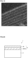
- FIG. 19 is an image showing an example of the HAADF-STEM image of the one hard particle of cutting tool 1 of the present embodiment.
- a layer shown in black is the region with a relatively low silicon concentration (silicon low-concentration layer)
- a layer shown in white or gray is the region with a relatively high silicon concentration (silicon high-concentration layer).
- a measurement region (size: 50 nm ⁇ 50 nm) is set so as to include a region in which seven or more layers of each of the silicon low-concentration layer shown in black and the silicon high-concentration layer shown in white or gray are stacked.
- a stacking direction of the silicon high-concentration layers and the silicon low-concentration layers is specified. Specifically, an electron beam diffraction pattern in the restricted field region and the stacking direction of the silicon high-concentration layers and the silicon low-concentration layers are overlapped, and the stacking direction is specified with the direction indicated by the diffraction spot.
- the measurement region contains titanium (Ti), silicon (Si), carbon (C), and nitrogen (N).
- a graph is prepared.
- the graph has coordinates of the X axis that indicates a distance from a beginning point of the measurement and the Y axis that indicates a percentage of the number of silicon atoms X Si to the total of the number of silicon atoms X Si and the number of titanium atoms, X Ti ⁇ Xsi/(Xsi + X Ti ) ⁇ 100.
- an average of the percentages ⁇ Xsi/(Xsi + X Ti ) ⁇ 100 (hereinafter, also referred to as "the average") in the measurement region is calculated.
- a region with a higher percentage ⁇ Xsi/(Xsi + X Ti ) ⁇ 100 than the average and a region with a lower percentage are alternately present.
- the region with a higher percentage ⁇ Xsi/(Xsi + X Ti ) ⁇ 100 than the average corresponds to the layer with a relatively high silicon concentration.
- the region with a lower percentage ⁇ Xsi/(Xsi + X T i) ⁇ 100 than the average corresponds to the layer with a relatively low silicon concentration.
- An average of periodic widths of the lamellar structure is preferably 3 nm or more and 20 nm or less. According to this, the distortion between the silicon high-concentration layer and the silicon low-concentration layer can be maintained to improve the breakage resistance, and cutting tool 1 can have a longer tool lifetime in the intermittent turning of steel in particular.
- the periodic width of the lamellar structure is referred to a distance from one silicon high-concentration layer to another silicon high-concentration layer adjacent to the one silicon high-concentration layer across the adjacent silicon low-concentration layer. This distance is referred to a distance between the middle points in the thickness direction of each layer of the silicon high-concentration layer and the other silicon high-concentration layer.
- the average of the periodic widths of the lamellar structure means an average of periodic widths of all the lamellar structures measured in the measurement region set in the above (C3).
- a method for measuring the periodic width of the silicon concentration herein is as follows.
- the measurement region is set by the same method as the above (A3) to (C3).
- the measurement region is subjected to a Fourier transformation to obtain a Fourier-transformed image (not illustrated).
- the periodicity in the measurement region appears as a spot.
- the periodic width is calculated by calculating a reciprocal of a distance between the above spot and an image center that indicates the maximum intensity in the Fourier-transformed image.
- a number of staking of the silicon high-concentration layer and the silicon low-concentration layer that constitute the lamellar structure is not particularly limited, and is preferably, for example, 10 or more and 1000 or less.
- the number of stackings is 10 or more, coarsening of crystal grains in each silicon high-concentration layer and each silicon low-concentration layer is inhibited, and the hardness of the hard particle can be maintained.
- the number of stackings is 1000 or less, the thickness of each silicon high-concentration layer and each silicon low-concentration layer can be sufficiently maintained, and mixing of unit layers can be inhibited.
- TiSiCN layer 30 preferably has a pillar structure.
- TiSiCN layer 30 has a pillar structure means "an average aspect ratio of the hard particles is 3 or more". According to this, TiSiCN layer 30 can exhibit high strength against stress into the shearing direction, and a micro cracking is inhibited to improve the wearing resistance. Thus, the cutting tool can have a longer tool lifetime, in particular, in intermittent turning of steel. Note that the average aspect ratio of the hard particles is measured by the following procedures (A4) to (D4).
- Cutting tool 1 is cut along the normal line of the surface of coating film 3 with a diamond wire to expose a cross section of TiSiCN layer 30.
- the exposed cross section is subjected to focused ion-beam process (hereinafter, also referred to as "FIB process") to allow the cross section to be a mirror state.
- FIB process focused ion-beam process
- a rectangular observation field is set.
- a pair of sides of the observation field is set to have a length of 30 ⁇ m in a direction parallel to the surface of substrate 2, and the other pair of sides is set to have a length that includes the entirety of TiSiCN layer 30 in the normal line direction to the surface of substrate 2 (thickness of TiSiCN layer 30).
- C4 Using a high-resolution electron backscatter diffraction apparatus, the observation field is analyzed with an interval of 0.02 ⁇ m to determine measurement points that have a cubic crystalline structure (hereinafter, also referred to as "cubic structure") in the observation field.
- a gap between a measurement point A that has the cubic structure and a measurement point B adjacent to the measurement point A is defined as the particle boundary when the gap between the measurement point A and the measurement point B has a direction difference of 5° or more.
- an outer circumference of the measurement point A is defined as the particle boundary.
- a particle that includes a measurement point that has a cubic structure in a region surrounded by the particle boundary is defined as one crystal grain.
- a specific measurement point has a direction difference of 5° or more from all the adjacent measurement points or when the measurement point has no cubic structure and is present alone, such a measurement point is not judged as a crystal grain. That is, a particle in which two or more measurement points are connected is treated as a crystal grain. According to this, the particle boundary is judged to specify the crystal grain.
- A1 to A20 each represent the aspect ratios A of the crystal grains (hard particles) P1 to P20.
- S1 to S20 each represent the areas S of the crystal grains (hard particles) P1 to P20.
- the obtained area-weighted average A ave herein corresponds to the average aspect ratio of the hard particles. It has been confirmed that, as long as the measurement is performed on the same specimen, the measurement results have almost no variation even when the measurement is performed a plurality of times with changing the observation field, and that the result is not willful even with randomly setting the observation field.
- TiSiCN layer 30 preferably has 90 vol% or more of the cubic crystalline structure. According to this, TiSiCN layer 30 can have higher hardness, and thereby cutting tool 1 can have more excellent wearing resistance. TiSiCN layer 30 more preferably has 92 vol% or more, further preferably 94 vol% or more, of the cubic crystalline structure. Although TiSiCN layer 30 most preferably has 100 vol% of the cubic crystalline structure, TiSiCN layer 30 can have 98 vol% or less, 96 vol% or less, or 95 vol% or less, thereof from the viewpoint of manufacturing.
- TiSiCN layer 30 preferably has 90 vol% or more and 100 vol% or less, more preferably 92 vol% or more and 98 vol% or less, and further preferably 94 vol% or more and 96 vol% or less, of the cubic crystalline structure.
- the proportion (percentage) of the cubic crystalline structure in TiSiCN layer 30 can be determined with formulation observation by using an electron backscattering diffraction apparatus. Specifically, the above (A4) to (C4) are firstly performed to specify a measurement point. Note that, in a direction mapping image (color map), a cubic crystalline part is indicated in "color other than black", and a part other than the cubic crystalline part is indicated in "black”. In the direction mapping image, an area proportion of the part in "color other than black” can be calculated to determine the proportion (percentage) of the cubic crystalline structure in TiSiCN layer 30.
- the method for manufacturing a cutting tool of the present embodiment is a method for manufacturing the cutting tool described in Embodiment 1, the method comprising:
- a substrate is prepared.
- a commercially available substrate may be used, or the substrate may be manufactured by common powder metallurgy.
- a WC powder, a Co powder, and the like are mixed with a ball mill and the like to obtain a mixed powder.
- the mixed powder is dried, the dried mixed powder is molded into a predetermined shape to obtain a molded product. Furthermore, the molded product is sintered to obtain WC-Co-based cemented carbide (sintered material).
- the sintered material can be subjected to a predetermined cutting-edge process, such as horning process, to manufacture a substrate composed of the WC-Co-based cemented carbide.
- a predetermined cutting-edge process such as horning process
- Any substrate other than the above can be prepared as long as the substrate is conventionally known as this kind of substrate.
- a coating film is formed on the substrate.
- the coating film is formed by using a CVD apparatus illustrated in Fig. 14 , for example.
- a CVD apparatus 50 a plurality of substrate-setting tools 52 that hold substrates 10 can be disposed, and these are covered by a reaction chamber 53 made of heat-resistant alloy steel.
- a temperature controller 54 is disposed, and a temperature in reaction chamber 53 can be controlled with this temperature controller 54.
- a nozzle 56 that has two inlets 55 and 57 are disposed.
- Nozzle 56 can have still another inlet (not illustrated).
- Nozzle 56 is disposed so as to penetrate a region where substrate-setting tools 52 are disposed.
- a plurality of jetting ports a first jetting port 61, a second jetting port 62, and a third jetting port (not illustrated) are formed.
- each gas introduced through inlets 55, 57 and the other inlet (not illustrated) into nozzle 56 is not mixed with each other in nozzle 56 to be introduced into reaction chamber 53 through jetting ports different from each other.
- This nozzle 56 can rotate with its axis as a central axis.
- an exhaust pipe 59 is disposed, and exhaust gas can be discharged outward through an exhaust port 60 of exhaust pipe 59.
- Tools and the like inside reaction chamber 53 are typically constituted with graphite.
- the TiSiCN layer is formed by a CVD method using the CVD apparatus.
- the step 2a includes a step 2a-1 of jetting TiCl 4 gas, SiCl 4 gas, and CH 3 CN gas toward the surface of the substrate.
- the TiCl 4 gas is jetted through a plurality of the second jetting ports provided on the nozzle of the CVD apparatus, and the SiCl 4 gas is jetted through a plurality of the first jetting ports provided on the nozzle.
- the CH 3 CN gas is jetted through a plurality of third jetting ports 63 ( Fig. 18 ) provided on the nozzle when nozzle 56 has still another inlet (not illustrated). When nozzle 56 does not have still another inlet port (not illustrated), the CH 3 CN gas is jetted through the plurality of the first jetting ports and the plurality of the second jetting ports.
- the nozzle rotates.
- Fig. 15 is an enlarged view of the region XV in Fig. 14 .
- Fig. 16 is an end face view of the nozzle in Fig. 15 , and is an end face view viewed from the arrow direction of the XVI-XVI line in Fig. 15 .
- Fig. 17 is an end face view of the nozzle in Fig. 15 , and is an end face view viewed from the arrow direction of the XVII-XVII line in Fig. 15 .
- first jetting port 61 is positioned with a distance from a standard height position HP, which is a height of a rake face of substrate 2 most close to the jetting port in CVD apparatus 50, to the lowest end of first jetting port 61 (in other words, a height d1 from the rake face) of 3 mm or more and 15 mm or less ( Figs. 15 and 16 ).
- second jetting port 62 is positioned with a distance from standard height position HP, which is a height of the rake face of substrate 2 most close to the jetting port in CVD apparatus 50, to the lowest end of the second jetting port 62 (in other words, a height d2 from the rake face (not illustrated)) of 0 mm or more and 2 mm or less ( Figs. 15 and 17 ). According to them, since second jetting port 62 is relatively close to a cutting edge region of the substrate, the TiCl 4 gas jetted through second jetting port 62 is relatively easily deposited in the cutting edge region, and relatively hardly deposited on the rake face.
- a flow rate of the SiCl 4 gas is set to be 1.0 ml/min or more and less than 6.0 ml/min. According to this, on the rake face in particular, excessive deposition of SiCl 4 can be inhibited.
- the TiSiCN layer has the first TiSiCN layer positioned in the rake face and the second TiSiCN layer positioned in the cutting edge region, the composition of the first TiSiCN layer is Ti (1-Xr )Si Xr CN, the composition of the second TiSiCN layer is Ti (1-Xe) Si Xe CN, and the Xr and the Xe each represent 0.010 or more and 0.100 or less, and satisfy a relationship of Xr - Xe ⁇ 0.003.” can be achieved. This is novelly found from intensive investigation by the present inventors.
- the composition of the gas jetted through the first jetting port can be SiCl 4 , H 2 , and N 2 ; the composition of the gas jetted through the second jetting port can be TiCl 4 , H 2 , and N 2 ; and the composition of the gas jetted through the third jetting port can be CH 3 CN and H 2 .
- the TiSiCN layer can be composed of the plurality of the hard particles, and the hard particles can have the lamellar structure in which the layer with a relatively high silicon concentration and the layer with a relatively low silicon concentration are alternately stacked.
- a rotation rate of the nozzle can be 1 rpm or more and 20 rpm or less.
- the average of the periodic widths of the lamellar structure can be regulated within the desired range.
- the rotation rate of the nozzle is preferably 1.5 rpm or more and 9.0 rpm or less.
- the average of the periodic widths of the lamellar structure can be regulated within "3 nm or more and 20 nm or less”.
- a film-forming temperature can be 800°C or more and 860°C or less.
- the TiSiCN layer can have the pillar structure.
- a furnace pressure can be 10 mbar or more and 65 mbar or less. According to this, the proportion (percentage) of the cubic crystalline structure in the TiSiCN layer can be regulated within the desired range.
- a film-forming time can be 2 hours or more and 25 hours or less. According to this, the thickness of the TiSiCN layer can be regulated within the desired range.
- the film-forming time is preferably 4.0 hours or more and 20.0 hours or less. According to this, the thickness of the TiSiCN layer can be regulated within 2.0 ⁇ m or more and 15 ⁇ m or less.
- a total gas flow rate of the reaction gases can be, for example, 120 to 200 L/min.
- total gas flow rate is referred to a total volumetric amount of gases, which is considered to the ideal gas at the standard condition (0°C, 1 atm) introduced into the CVD furnace per unit time.
- the coating film formed in the second step includes the TiSiCN layer.
- This TiSiCN layer has: the first TiSiCN layer positioned in the rake face; and the second TiSiCN layer positioned in the cutting edge region, the composition of the first TiSiCN layer is Ti (1-Xr )Si Xr CN, the composition of the second TiSiCN layer is Ti(i-xe)SixeCN, and the Xr and the Xe each represent 0.010 or more and 0.100 or less, and satisfy a relationship of Xr - Xe ⁇ 0.003.
- a surface treatment step such as surface polishing and shot blast can be performed.
- the coating film includes other layers (such as a base layer), these layers can be formed by a conventionally known method.
- raw material powders composed of a cutting insert for turning made of cemented carbide Co (6 wt%)-VC (0.2 wt%)-Cr3C2 (0.4 wt%)-WC (remainder) were uniformly mixed, pressure-molded into a predetermined shape, and then sintered at 1300 to 1500°C for 1 to 2 hours to obtain a substrate CNMG120408N-GU (manufactured by Sumitomo Electric Hardmetal Corp.).
- a base layer (TiN layer) was formed on a surface of each substrate obtained in the above. Specifically, the substrate was set in a reaction furnace of a chemical vapor deposition apparatus to form the base layer on the substrate by the chemical vapor deposition. A condition for forming the base layer is as shown in the following Table 1.
- a coating film was formed on the surface of each substrate obtained in the above. Specifically, the substrate was set in a reaction furnace of a chemical vapor deposition apparatus to form the coating film on the substrate by the chemical vapor deposition. A condition for forming the coating film is as shown in the following Table 2.
- each Sample was set in a reaction furnace of a chemical vapor deposition apparatus, and the chemical vapor deposition was performed under a condition for forming the intermediate layer shown in Table 3 to form the intermediate layer on the TiSiCN layer. Thereafter, the chemical vapor deposition was performed under a condition for forming the surface layer shown in Table 4 to form the surface layer on the intermediate layer.
- the thickness of the base layer was determined by the method described in Embodiment 1. Each of the obtained results is shown in “Thickness of base layer [ ⁇ m]” of Table 5.
- the thickness of the TiSiCN layer was determined by the method described in Embodiment 1. Each of the obtained results is shown in "Thickness of TiSiCN layer [ ⁇ m]” of Table 5.
- the thickness of the intermediate layer was determined by the method described in Embodiment 1.
- This cutting condition corresponds to the intermittent turning of steel.
- the cutting tools of Samples 1-1 to 1-12-3 correspond to Examples.
- Samples 1-101 to 1-104 correspond to Comparative Examples. It has been confirmed that the cutting tools of Samples 1-1 to 1-12-3 (Examples) have a longer tool lifetime than the cutting tools of Samples 1-101 to 1-104 (Comparative Examples) even in the intermittent turning of steel.
- a substrate same as the substrates of Samples 1-1 to 1-12-3 and 1-101 to 1-104 was prepared.
- a base layer (TiN layer) was formed on a surface of each substrate obtained in the above. Specifically, the substrate was set in a reaction furnace of a chemical vapor deposition apparatus to form the base layer on the substrate by the chemical vapor deposition. A condition for forming the base layer is as shown in the following Table 6.
- a coating film was formed on the surface of each substrate obtained in the above. Specifically, the substrate was set in a reaction furnace of a chemical vapor deposition apparatus to form the coating film on the substrate by the chemical vapor deposition. A condition for forming the coating film is as shown in the following Table 7.
- each Sample was set in a reaction furnace of a chemical vapor deposition apparatus, and the chemical vapor deposition was performed under a condition for forming the intermediate layer shown in Table 8 to form the intermediate layer on the TiSiCN layer. Thereafter, the chemical vapor deposition was performed under a condition for forming the surface layer shown in Table 9 to form the surface layer on the intermediate layer.
- the thickness of the base layer was determined by the method described in Embodiment 1. Each of the obtained results is shown in “Thickness of base layer [ ⁇ m]” of Table 10.
- the thickness of the TiSiCN layer was determined by the method described in Embodiment 1.
- the thickness of the intermediate layer was determined by the method described in Embodiment 1.
- This cutting condition corresponds to the intermittent turning of steel.
- the cutting tools of Samples 2-1 to 2-11-3 correspond to Examples.
- Samples 2-101 to 2-104 correspond to Comparative Examples. It has been confirmed that the cutting tools of Samples 2-1 to 2-11-3 (Examples) have a longer tool lifetime than the cutting tools of Samples 2-101 to 2-104 (Comparative Examples) even in the intermittent turning of steel.
- a substrate same as the substrates of Samples 1- 1 to 1-12-3 and 1-101 to 1-104 was prepared.
- a base layer (TiN layer) was formed on a surface of each substrate obtained in the above. Specifically, the substrate was set in a reaction furnace of a chemical vapor deposition apparatus to form the base layer on the substrate by the chemical vapor deposition. A condition for forming the base layer was as shown in the following Table 11.
- a coating film was formed on the surface of each substrate obtained in the above. Specifically, the substrate was set in a reaction furnace of a chemical vapor deposition apparatus to form the coating film on the substrate by the chemical vapor deposition. A condition for forming the coating film is as shown in the following Table 12.
- each Sample was set in a reaction furnace of a chemical vapor deposition apparatus, and the chemical vapor deposition was performed under a condition for forming the intermediate layer shown in Table 13 to form the intermediate layer on the TiSiCN layer. Thereafter, the chemical vapor deposition was performed under a condition for forming the surface layer shown in Table 14 to form the surface layer on the intermediate layer.
- the Xr was determined by the method described in Embodiment 1. Each of the obtained results is shown in "Xr (rake face)" of Table 15. Of the cutting tools of Samples 3-1 to 3-10-3 and 3-101 to 3-104, the Xe was determined by the method described in Embodiment 1. Each of the obtained results is shown in "Xe (cutting edge)" of Table 15.
- the thickness of the base layer was determined by the method described in Embodiment 1. Each of the obtained results is shown in “Thickness of base layer [ ⁇ m]” of Table 15. Of the cutting tools of Samples 3-1 to 3-10-3, and 3-101 to 3-104, the thickness of the TiSiCN layer was determined by the method described in Embodiment 1. Each of the obtained results is shown in "Thickness of TiSiCN layer [ ⁇ m]" of Table 15. Of the cutting tools of Samples 3-1 to 3-10-1, and 3-101 to 3-104, the thickness of the intermediate layer was determined by the method described in Embodiment 1.
- This cutting condition corresponds to the intermittent turning of steel.
- the cutting tools of Samples 3-1 to 3-10-3 correspond to Examples.
- Samples 3-101 to 3-104 correspond to Comparative Examples. It has been confirmed that the cutting tools of Samples 3-1 to 3-10-3 (Examples) have a longer tool lifetime than the cutting tools of Samples 3-101 to 3-104 (Comparative Examples) even in the intermittent turning of steel.
Landscapes
- Chemical & Material Sciences (AREA)
- Engineering & Computer Science (AREA)
- Mechanical Engineering (AREA)
- Chemical Kinetics & Catalysis (AREA)
- Organic Chemistry (AREA)
- Metallurgy (AREA)
- Materials Engineering (AREA)
- Inorganic Chemistry (AREA)
- General Chemical & Material Sciences (AREA)
- Life Sciences & Earth Sciences (AREA)
- Geology (AREA)
- Mining & Mineral Resources (AREA)
- Environmental & Geological Engineering (AREA)
- Geochemistry & Mineralogy (AREA)
- General Life Sciences & Earth Sciences (AREA)
- Fluid Mechanics (AREA)
- Physics & Mathematics (AREA)
- Ceramic Engineering (AREA)
- Cutting Tools, Boring Holders, And Turrets (AREA)
Applications Claiming Priority (1)
| Application Number | Priority Date | Filing Date | Title |
|---|---|---|---|
| PCT/JP2022/032595 WO2024047752A1 (fr) | 2022-08-30 | 2022-08-30 | Outil de coupe |
Publications (2)
| Publication Number | Publication Date |
|---|---|
| EP4454792A1 true EP4454792A1 (fr) | 2024-10-30 |
| EP4454792A4 EP4454792A4 (fr) | 2024-11-27 |
Family
ID=89534315
Family Applications (1)
| Application Number | Title | Priority Date | Filing Date |
|---|---|---|---|
| EP22957355.5A Pending EP4454792A4 (fr) | 2022-08-30 | 2022-08-30 | Outil de coupe |
Country Status (5)
| Country | Link |
|---|---|
| US (1) | US11975391B2 (fr) |
| EP (1) | EP4454792A4 (fr) |
| JP (1) | JP7416327B1 (fr) |
| CN (1) | CN118524901B (fr) |
| WO (1) | WO2024047752A1 (fr) |
Cited By (1)
| Publication number | Priority date | Publication date | Assignee | Title |
|---|---|---|---|---|
| EP4357053B1 (fr) * | 2022-08-30 | 2026-03-11 | Sumitomo Electric Industries, Ltd. | Outil de coupe |
Families Citing this family (2)
| Publication number | Priority date | Publication date | Assignee | Title |
|---|---|---|---|---|
| KR102450097B1 (ko) * | 2020-11-16 | 2022-10-05 | 한국야금 주식회사 | 절삭공구용 경질 피막 |
| WO2025013293A1 (fr) * | 2023-07-13 | 2025-01-16 | 住友電気工業株式会社 | Outil de coupe |
Family Cites Families (13)
| Publication number | Priority date | Publication date | Assignee | Title |
|---|---|---|---|---|
| JPH10280148A (ja) * | 1997-04-09 | 1998-10-20 | Hitachi Tool Eng Co Ltd | 被覆硬質部材 |
| US8247092B2 (en) * | 2007-04-18 | 2012-08-21 | Sandvik Intellectual Property Ab | Coated cutting tool and a method of making thereof |
| IL182741A (en) * | 2007-04-23 | 2012-03-29 | Iscar Ltd | Coatings |
| SE531704C2 (sv) * | 2007-07-13 | 2009-07-14 | Seco Tools Ab | Finkornig hårdmetall för svarvning av varmhållfasta superlegeringar (HRSA) |
| KR101685450B1 (ko) * | 2010-09-29 | 2016-12-12 | 쿄세라 코포레이션 | 절삭 공구 |
| JP2012030359A (ja) * | 2011-09-21 | 2012-02-16 | Sumitomo Electric Hardmetal Corp | 刃先交換型切削チップ |
| DE102011087715A1 (de) | 2011-12-05 | 2013-07-25 | Fraunhofer-Gesellschaft zur Förderung der angewandten Forschung e.V. | Hartstoffbeschichtete körper aus metall, hartmetall, cermet oder keramik sowie verfahren zur herstellung derartiger körper |
| CN104870127B (zh) * | 2012-12-27 | 2017-03-08 | 京瓷株式会社 | 切削工具 |
| DE102017102642A1 (de) | 2017-02-10 | 2018-08-16 | Fraunhofer-Gesellschaft zur Förderung der angewandten Forschung e. V. | Hartstoffbeschichtete Körper aus Metall, Hartmetall, Cermet oder Keramik und Verfahren zur Herstellung derartiger Körper |
| WO2019181220A1 (fr) * | 2018-03-19 | 2019-09-26 | 住友電工ハードメタル株式会社 | Outil de coupe à revêtement de surface |
| CN110129742B (zh) * | 2019-06-24 | 2022-03-11 | 哈尔滨工业大学 | 一种超硬强韧TiSiCN硬质涂层的制备方法 |
| CN114836754B (zh) * | 2022-04-27 | 2023-04-28 | 赣州澳克泰工具技术有限公司 | 一种带涂层的切削工具及其制备方法 |
| JP7416328B1 (ja) * | 2022-08-30 | 2024-01-17 | 住友電気工業株式会社 | 切削工具 |
-
2022
- 2022-08-30 JP JP2023503206A patent/JP7416327B1/ja active Active
- 2022-08-30 US US18/026,595 patent/US11975391B2/en active Active
- 2022-08-30 CN CN202280088021.6A patent/CN118524901B/zh active Active
- 2022-08-30 WO PCT/JP2022/032595 patent/WO2024047752A1/fr not_active Ceased
- 2022-08-30 EP EP22957355.5A patent/EP4454792A4/fr active Pending
Cited By (1)
| Publication number | Priority date | Publication date | Assignee | Title |
|---|---|---|---|---|
| EP4357053B1 (fr) * | 2022-08-30 | 2026-03-11 | Sumitomo Electric Industries, Ltd. | Outil de coupe |
Also Published As
| Publication number | Publication date |
|---|---|
| JPWO2024047752A1 (fr) | 2024-03-07 |
| US11975391B2 (en) | 2024-05-07 |
| JP7416327B1 (ja) | 2024-01-17 |
| CN118524901A (zh) | 2024-08-20 |
| WO2024047752A1 (fr) | 2024-03-07 |
| EP4454792A4 (fr) | 2024-11-27 |
| US20240066605A1 (en) | 2024-02-29 |
| CN118524901B (zh) | 2026-04-17 |
Similar Documents
| Publication | Publication Date | Title |
|---|---|---|
| EP4454792A1 (fr) | Outil de coupe | |
| EP4494788B1 (fr) | Outil de coupe | |
| EP4331755A1 (fr) | Outil de coupe | |
| EP4331758A1 (fr) | Outil de coupe et procédé de fabrication associé | |
| EP4357053B1 (fr) | Outil de coupe | |
| EP4292736B1 (fr) | Outil de coupe et procédé de fabrication associé | |
| EP3851230B1 (fr) | Outil de coupe | |
| US12350742B2 (en) | Surface-coated cutting tool | |
| JP7338827B1 (ja) | 切削工具 | |
| EP3868502B1 (fr) | Outil de coupe | |
| EP3868501B1 (fr) | Outil de coupe | |
| EP4729217A1 (fr) | Outil de coupe | |
| EP4613406A1 (fr) | Outil de coupe | |
| EP4729216A1 (fr) | Outil de coupe | |
| EP4091748B1 (fr) | Outils de coupe | |
| EP4088841B1 (fr) | Outils de coupe | |
| EP4091747B1 (fr) | Outils de coupe | |
| EP4331756A1 (fr) | Outil de coupe | |
| EP4331757A1 (fr) | Outil de coupe | |
| EP4527527A1 (fr) | Outil de coupe | |
| EP4575034A1 (fr) | Outil de coupe | |
| WO2023276209A1 (fr) | Outil revêtu | |
| JP2025147873A (ja) | 表面被覆切削工具 | |
| JP2022139720A (ja) | 表面被覆切削工具 |
Legal Events
| Date | Code | Title | Description |
|---|---|---|---|
| STAA | Information on the status of an ep patent application or granted ep patent |
Free format text: STATUS: THE INTERNATIONAL PUBLICATION HAS BEEN MADE |
|
| PUAI | Public reference made under article 153(3) epc to a published international application that has entered the european phase |
Free format text: ORIGINAL CODE: 0009012 |
|
| STAA | Information on the status of an ep patent application or granted ep patent |
Free format text: STATUS: REQUEST FOR EXAMINATION WAS MADE |
|
| 17P | Request for examination filed |
Effective date: 20240723 |
|
| AK | Designated contracting states |
Kind code of ref document: A1 Designated state(s): AL AT BE BG CH CY CZ DE DK EE ES FI FR GB GR HR HU IE IS IT LI LT LU LV MC MK MT NL NO PL PT RO RS SE SI SK SM TR |
|
| A4 | Supplementary search report drawn up and despatched |
Effective date: 20241028 |
|
| RIC1 | Information provided on ipc code assigned before grant |
Ipc: C23C 16/455 20060101ALI20241022BHEP Ipc: C23C 16/36 20060101ALI20241022BHEP Ipc: C23C 30/00 20060101ALI20241022BHEP Ipc: C23C 28/04 20060101ALI20241022BHEP Ipc: B23B 27/14 20060101AFI20241022BHEP |
|
| DAV | Request for validation of the european patent (deleted) | ||
| DAX | Request for extension of the european patent (deleted) |