EP4447472A1 - Stacked filter assembly for optical integrated circuit package with an optical filter mounted to an optical integrated circuit device by a discrete semiconductor spacer block - Google Patents
Stacked filter assembly for optical integrated circuit package with an optical filter mounted to an optical integrated circuit device by a discrete semiconductor spacer block Download PDFInfo
- Publication number
- EP4447472A1 EP4447472A1 EP24169015.5A EP24169015A EP4447472A1 EP 4447472 A1 EP4447472 A1 EP 4447472A1 EP 24169015 A EP24169015 A EP 24169015A EP 4447472 A1 EP4447472 A1 EP 4447472A1
- Authority
- EP
- European Patent Office
- Prior art keywords
- parallelpipedal
- optical filter
- integrated circuit
- sensor array
- edge
- Prior art date
- Legal status (The legal status is an assumption and is not a legal conclusion. Google has not performed a legal analysis and makes no representation as to the accuracy of the status listed.)
- Pending
Links
Images



Classifications
-
- H—ELECTRICITY
- H04—ELECTRIC COMMUNICATION TECHNIQUE
- H04N—PICTORIAL COMMUNICATION, e.g. TELEVISION
- H04N23/00—Cameras or camera modules comprising electronic image sensors; Control thereof
- H04N23/50—Constructional details
- H04N23/55—Optical parts specially adapted for electronic image sensors; Mounting thereof
-
- G—PHYSICS
- G01—MEASURING; TESTING
- G01S—RADIO DIRECTION-FINDING; RADIO NAVIGATION; DETERMINING DISTANCE OR VELOCITY BY USE OF RADIO WAVES; LOCATING OR PRESENCE-DETECTING BY USE OF THE REFLECTION OR RERADIATION OF RADIO WAVES; ANALOGOUS ARRANGEMENTS USING OTHER WAVES
- G01S7/00—Details of systems according to groups G01S13/00, G01S15/00, G01S17/00
- G01S7/48—Details of systems according to groups G01S13/00, G01S15/00, G01S17/00 of systems according to group G01S17/00
- G01S7/483—Details of pulse systems
- G01S7/486—Receivers
- G01S7/4865—Time delay measurement, e.g. time-of-flight measurement, time of arrival measurement or determining the exact position of a peak
-
- G—PHYSICS
- G02—OPTICS
- G02B—OPTICAL ELEMENTS, SYSTEMS OR APPARATUS
- G02B6/00—Light guides; Structural details of arrangements comprising light guides and other optical elements, e.g. couplings
- G02B6/10—Light guides; Structural details of arrangements comprising light guides and other optical elements, e.g. couplings of the optical waveguide type
- G02B6/12—Light guides; Structural details of arrangements comprising light guides and other optical elements, e.g. couplings of the optical waveguide type of the integrated circuit kind
- G02B6/122—Basic optical elements, e.g. light-guiding paths
-
- G—PHYSICS
- G01—MEASURING; TESTING
- G01S—RADIO DIRECTION-FINDING; RADIO NAVIGATION; DETERMINING DISTANCE OR VELOCITY BY USE OF RADIO WAVES; LOCATING OR PRESENCE-DETECTING BY USE OF THE REFLECTION OR RERADIATION OF RADIO WAVES; ANALOGOUS ARRANGEMENTS USING OTHER WAVES
- G01S17/00—Systems using the reflection or reradiation of electromagnetic waves other than radio waves, e.g. lidar systems
- G01S17/02—Systems using the reflection of electromagnetic waves other than radio waves
- G01S17/06—Systems determining position data of a target
- G01S17/08—Systems determining position data of a target for measuring distance only
- G01S17/10—Systems determining position data of a target for measuring distance only using transmission of interrupted, pulse-modulated waves
-
- G—PHYSICS
- G02—OPTICS
- G02B—OPTICAL ELEMENTS, SYSTEMS OR APPARATUS
- G02B6/00—Light guides; Structural details of arrangements comprising light guides and other optical elements, e.g. couplings
- G02B6/10—Light guides; Structural details of arrangements comprising light guides and other optical elements, e.g. couplings of the optical waveguide type
- G02B6/12—Light guides; Structural details of arrangements comprising light guides and other optical elements, e.g. couplings of the optical waveguide type of the integrated circuit kind
-
- H—ELECTRICITY
- H04—ELECTRIC COMMUNICATION TECHNIQUE
- H04N—PICTORIAL COMMUNICATION, e.g. TELEVISION
- H04N23/00—Cameras or camera modules comprising electronic image sensors; Control thereof
- H04N23/57—Mechanical or electrical details of cameras or camera modules specially adapted for being embedded in other devices
-
- H—ELECTRICITY
- H10—SEMICONDUCTOR DEVICES; ELECTRIC SOLID-STATE DEVICES NOT OTHERWISE PROVIDED FOR
- H10F—INORGANIC SEMICONDUCTOR DEVICES SENSITIVE TO INFRARED RADIATION, LIGHT, ELECTROMAGNETIC RADIATION OF SHORTER WAVELENGTH OR CORPUSCULAR RADIATION
- H10F55/00—Radiation-sensitive semiconductor devices covered by groups H10F10/00, H10F19/00 or H10F30/00 being structurally associated with electric light sources and electrically or optically coupled thereto
- H10F55/20—Radiation-sensitive semiconductor devices covered by groups H10F10/00, H10F19/00 or H10F30/00 being structurally associated with electric light sources and electrically or optically coupled thereto wherein the electric light source controls the radiation-sensitive semiconductor devices, e.g. optocouplers
- H10F55/25—Radiation-sensitive semiconductor devices covered by groups H10F10/00, H10F19/00 or H10F30/00 being structurally associated with electric light sources and electrically or optically coupled thereto wherein the electric light source controls the radiation-sensitive semiconductor devices, e.g. optocouplers wherein the radiation-sensitive devices and the electric light source are all semiconductor devices
- H10F55/255—Radiation-sensitive semiconductor devices covered by groups H10F10/00, H10F19/00 or H10F30/00 being structurally associated with electric light sources and electrically or optically coupled thereto wherein the electric light source controls the radiation-sensitive semiconductor devices, e.g. optocouplers wherein the radiation-sensitive devices and the electric light source are all semiconductor devices formed in, or on, a common substrate
-
- H—ELECTRICITY
- H10—SEMICONDUCTOR DEVICES; ELECTRIC SOLID-STATE DEVICES NOT OTHERWISE PROVIDED FOR
- H10F—INORGANIC SEMICONDUCTOR DEVICES SENSITIVE TO INFRARED RADIATION, LIGHT, ELECTROMAGNETIC RADIATION OF SHORTER WAVELENGTH OR CORPUSCULAR RADIATION
- H10F77/00—Constructional details of devices covered by this subclass
- H10F77/30—Coatings
- H10F77/306—Coatings for devices having potential barriers
- H10F77/331—Coatings for devices having potential barriers for filtering or shielding light, e.g. multicolour filters for photodetectors
-
- H—ELECTRICITY
- H10—SEMICONDUCTOR DEVICES; ELECTRIC SOLID-STATE DEVICES NOT OTHERWISE PROVIDED FOR
- H10F—INORGANIC SEMICONDUCTOR DEVICES SENSITIVE TO INFRARED RADIATION, LIGHT, ELECTROMAGNETIC RADIATION OF SHORTER WAVELENGTH OR CORPUSCULAR RADIATION
- H10F77/00—Constructional details of devices covered by this subclass
- H10F77/50—Encapsulations or containers
-
- G—PHYSICS
- G02—OPTICS
- G02B—OPTICAL ELEMENTS, SYSTEMS OR APPARATUS
- G02B6/00—Light guides; Structural details of arrangements comprising light guides and other optical elements, e.g. couplings
- G02B6/10—Light guides; Structural details of arrangements comprising light guides and other optical elements, e.g. couplings of the optical waveguide type
- G02B6/12—Light guides; Structural details of arrangements comprising light guides and other optical elements, e.g. couplings of the optical waveguide type of the integrated circuit kind
- G02B2006/12083—Constructional arrangements
- G02B2006/12085—Integrated
-
- G—PHYSICS
- G02—OPTICS
- G02B—OPTICAL ELEMENTS, SYSTEMS OR APPARATUS
- G02B6/00—Light guides; Structural details of arrangements comprising light guides and other optical elements, e.g. couplings
- G02B6/10—Light guides; Structural details of arrangements comprising light guides and other optical elements, e.g. couplings of the optical waveguide type
- G02B6/12—Light guides; Structural details of arrangements comprising light guides and other optical elements, e.g. couplings of the optical waveguide type of the integrated circuit kind
- G02B2006/12083—Constructional arrangements
- G02B2006/12109—Filter
-
- H—ELECTRICITY
- H10—SEMICONDUCTOR DEVICES; ELECTRIC SOLID-STATE DEVICES NOT OTHERWISE PROVIDED FOR
- H10F—INORGANIC SEMICONDUCTOR DEVICES SENSITIVE TO INFRARED RADIATION, LIGHT, ELECTROMAGNETIC RADIATION OF SHORTER WAVELENGTH OR CORPUSCULAR RADIATION
- H10F77/00—Constructional details of devices covered by this subclass
- H10F77/40—Optical elements or arrangements
Definitions
- the present invention generally relates to an optical integrated circuit package and, in particular, to the mounting of an optical filter to extend over an optical sensor of an optical integrated circuit device.
- a bead of adhesive material perhaps containing a spacer material (such as beads of uniform size) is deposited on the upper surface of the optical integrated circuit device in a continuous ring shape around the optical sensor.
- the optical filter is then placed over the optical sensor in a spaced-apart relationship set by the dimension of the spacer beads and secured to the optical integrated circuit device using the adhesive material of the spacer ring.
- a spacer layer made of an insulating material such as FR4-type material
- the optical filter is then placed over the optical sensor in a spaced-apart relationship set by the thickness of the spacer layer and secured by an adhesive layer to the upper surface of the spacer layer.
- a device comprises: a support substrate; an optical integrated circuit device mounted over an upper surface of the support substrate; wherein said optical integrated circuit device includes an optical sensor array supported by a semiconductor substrate made of a first semiconductor material; a first discrete semiconductor block made of a second semiconductor material; wherein the first and second semiconductor materials have substantially matched coefficients of thermal expansion; wherein the first discrete semiconductor block is mounted over an upper surface of the optical integrated circuit device adjacent the optical sensor array; and a parallelpipedal-shaped optical filter mounted over an upper surface of the first discrete semiconductor block and extending over the optical sensor array.
- one or more edges or corners of the parallelpipedal-shaped optical filter lack any form of support.
- the device includes just one discrete semiconductor block supporting the parallelpipedal-shaped optical filter.
- the device includes just two discrete semiconductor blocks supporting the parallelpipedal-shaped optical filter.
- one edge of the parallelpipedal-shaped optical filter is supported by the discrete semiconductor block, while another edge opposite said one edge is not supported at all.
- one corner of the parallelpipedal-shaped optical filter is supported by the discrete semiconductor block, while another corner opposite said one corner is not supported at all.
- a center of the parallelpipedal-shaped optical filter between opposite edges is supported by the discrete semiconductor block, while neither of said opposite edges is supported at all.
- the device further comprises a cap mounted over the upper surface of the support substrate.
- the cap includes walls delimiting a cavity within which the optical sensor array is located.
- a wall opening in said cap is aligned with the optical sensor array, and a diffractive optical element (such as lens) is mounted at the wall opening.
- a support substrate 102 is made of an insulating material (perhaps including multiple layers) and includes an upper surface and a lower surface.
- the support substrate 102 may, for example, be of a printed circuit board (PCB) type.
- the upper surface of support substrate 102 is covered by a first solder mask layer 104 including openings that expose upper circuit connection pads.
- the lower surface of support substrate 102 is covered by a second solder mask layer 108 including openings that expose lower circuit pads.
- the upper circuit connection pads are electrically connected to the lower circuit pads through an electrical interconnection network (not explicitly shown) within the support substrate 102.
- a lower (or back) surface of an optical sensor integrated circuit (IC) device i.e., an IC die
- IC optical sensor integrated circuit
- the optical sensor integrated circuit device 112 includes, at its upper (or front) surface, a first optical sensor array 116A and a second optical sensor array 116B (i.e., a front-side illuminated sensor) supported by a semiconductor material substrate.
- the arrays 116A and 116B include one or more photosensitive circuits formed on and/or in the semiconductor material substrate such as, for example, single photon avalanche diodes (SPADs).
- SPADs single photon avalanche diodes
- wirebonding is shown by example, it will be understood that the optical sensor integrated circuit device 112 may instead be surface mounted, in a flip-chip configuration, to certain ones of the upper circuit connection pads located within an opening in the first solder mask layer 104, with the first optical sensor array 116A and second optical sensor array 116B provided at a lower (or back) surface (i.e., a back-side illuminated sensor).
- An optical emitter integrated circuit device 122 is surface mounted to certain one(s) of the upper circuit connection pads within corresponding opening(s) in the first solder mask layer 104 and wirebonded to certain other one(s) of the upper circuit connection pads within corresponding opening(s) in the first solder mask layer 104.
- Auxiliary circuit components 128 are surface mounted to certain ones of the upper circuit connection pads within corresponding openings in the first solder mask layer 104.
- the illustrated circuitry may, for example, form a time-of-flight sensing circuit where the optical emitter integrated circuit device 122 is configured to emit a pulse of (infrared) light that is sensed by the first optical sensor array 116A of the optical sensor integrated circuit device 112 to provide a reference time for light emission, with a target reflection of the emitted pulse of light being sensed by the second optical sensor array 116B of the optical sensor integrated circuit device 112 to provide a detection time for light reflection. Distance from the optical integrated circuit package to the target may then be calculated as a function of the time difference between the reference time and the detection time. Power connections and signal connections for the portion 100 are provided through the lower circuit pads exposed by the openings in the second solder mask layer 108.
- An optical filter 132 is mounted to extend over the second optical sensor array 116B of the optical sensor integrated circuit device 112.
- the optical filter 132 may, for example, be configured to selectively pass light within a certain range of wavelengths (for example, infrared) corresponding to a wavelength of the light emitted by the optical emitter integrated circuit device 122.
- the optical filter 132 is configured as a flat rectangular plate that has, for example, a parallelpipedal shape (i.e., a six-faced polyhedron all of whose faces are parallelograms lying in pairs of parallel planes).
- the major (i.e., top and bottom) faces of the parallelpipedal-shaped optical filter 132 extend in the x-y plane parallel to the upper surface of the optical sensor integrated circuit device 112 and completely cover the second optical sensor array 116B.
- the minor (i.e., side or peripheral edge) faces of the parallelpipedal-shaped optical filter 132 extend in the z-direction perpendicular to the upper surface of the optical sensor integrated circuit device 112.
- a pair of spacer blocks 136 are provided with one spacer block arranged to longitudinally extend (for example, in the x-direction) parallel to a first side edge of the optical filter 132 and another spacer block arranged to longitudinally extend (for example, in the y-direction) parallel to a second side edge of the optical filter 132 (where the first and second side edges are adjacent each other).
- the spacer blocks 136 which have a thickness in the z-direction substantially equal to a desired z-direction offset of the optical filter 132 from the upper surface of the optical sensor integrated circuit device 112, are each made of a silicon material formed as a flat rectangular plate (having, for example, a parallelpipedal shape).
- the bottom surface of each spacer block is attached, for example using a layer of adhesive material (for example, comprising a die attach film (DAF) layer), to the upper surface of the optical sensor integrated circuit device 112.
- the bottom surface of the optical filter 132 is attached, for example using a layer of adhesive material (for example, comprising a die attach film (DAF) layer), to the upper surfaces of the spacer blocks 136.
- the spacer blocks 136 may, for example, be manufactured by singulating (i.e., dicing) a wafer of semiconductor (for example, silicon) material having a desired thickness in the z direction into desired sizes in the x-y plane.
- the semiconductor material of the wafer used to make the spacer blocks and the semiconductor substrate material of the optical sensor integrated circuit device 112 are preferably a same semiconductor material (having identical coefficients of thermal expansion) or semiconductor materials have substantially similar coefficients of thermal expansion (for example, +/- 5% of each other).
- the diced portions of the wafer forming the spacer blocks 136 are then positioned, for example using a suitable pick-and-place manufacturing operation, at desired locations on the upper surface of the optical sensor integrated circuit device 112.
- These desired locations may comprise, for example, free areas at the upper surface of the optical sensor integrated circuit device 112 where neither the first optical sensor array 116A, nor the second optical sensor array 116B, nor the electrical pads 120 of the optical sensor integrated circuit device 112 are located.
- the free areas where the spacer blocks 136 are positioned for attachment may comprise areas along a side edge of the second optical sensor array 116B and/or between the side edge of the second optical sensor array 116B and the electrical pads of the optical sensor integrated circuit device 112.
- the adhesive material layers 138 may, for example, be provided at upper and lower surfaces of the wafer of semiconductor prior to singulation.
- the optical filter 132 may, for example, be manufactured by singulating (i.e., dicing) a wafer of transparent (for example, glass) material having desired thickness in the z direction into desired sizes in the x-y plane. The diced portion of the wafer forming the optical filter 132 is then positioned, for example using a suitable pick-and-place manufacturing operation, at a desired location on the spacer block (s) 136 and extending over at least the second optical sensor array 116B.
- singulating i.e., dicing
- a wafer of transparent (for example, glass) material having desired thickness in the z direction into desired sizes in the x-y plane.
- the diced portion of the wafer forming the optical filter 132 is then positioned, for example using a suitable pick-and-place manufacturing operation, at a desired location on the spacer block (s) 136 and extending over at least the second optical sensor array 116B.
- Suitable ultra-violet (UV) exposure may be used to activate and cure the adhesive material of the layers 138 during manufacture of the portion 100.
- At least one corner of the optical filter 132, and perhaps two or more distal portions of side edges of the optical filter 132, are not supported at all by a spacer block 136. That at least one corner and/or two or more distal portions of side edges of the optical filter 132 extend unsupported, in a cantilever-like fashion, over the second optical sensor array 116B of the optical sensor integrated circuit device 112.
- the corner 150 and/or the distal portions 152, 154 of adjacent side edges are unsupported by the spacer blocks 136.
- a first edge of the parallelpipedal-shaped optical filter 132 is supported by the discrete spacer block 136 and a second edge of the parallelpipedal-shaped optical filter 132 opposite the first edge is not supported at all (see, Figure 5 , for example).
- a first corner of the parallelpipedal-shaped optical filter 132 is supported by the discrete spacer block(s) 136 and a second corner of the parallelpipedal-shaped optical filter diagonally opposite the first corner is not supported at all by a spacer (see, Figure 2 , for example).
- the parallelpipedal-shaped optical filter 132 includes a first edge and a second edge opposite the first edge of the parallelpipedal-shaped optical filter, with the discrete spacer block 136 positioned between the first and second edges, and neither of the opposed first and second edges of the parallelpipedal-shaped optical filter 132 is supported at all by a spacer.
- the parallelpipedal-shaped optical filter 132 includes a first edge and a second edge adjacent the first edge, with one discrete spacer block 136 positioned adjacent the first edge of the parallelpipedal-shaped optical filter, and another discrete spacer block 136 positioned adjacent the second edge of the parallelpipedal-shaped optical filter (see, Figure 2 , for example). In this case, it will be noted that a corner of the parallelpipedal-shaped optical filter 132 diagonally opposite a corner at the adjacent first and second edges of the parallelpipedal-shaped optical filter 132 is not supported at all by a spacer.
- FIG. 4 illustrates a cross sectional perspective view of an optical integrated circuit package 200 including the portion 100 of Figures 1 and 2 .
- a cap 202 is mounted to the upper surface of the first solder mask layer 104.
- the cap includes side walls 204, a front wall 206 over the side walls and a partition wall 208 extending between an opposed pair of side walls.
- the partition wall 208 is arranged to be placed between the first optical sensor array 116A and the second optical sensor array 116B of the optical sensor integrated circuit device 112.
- the side walls 204, front wall 206 and partition wall 208 delimit two cavities within the cap 202.
- the first cavity 210A includes the optical emitter integrated circuit device 122 and a portion of the optical sensor integrated circuit device 112 which includes the first optical sensor array 116A.
- the second cavity 210B includes a portion of the optical sensor integrated circuit device 112 which includes the second optical sensor array 116B.
- the partition wall 208 provides a light barrier for blocking light emitted by the optical emitter integrated circuit device 122 from directly reaching the second optical sensor array 116B (in other words, the emitted light is block from propagating within the confines of the cap 202 to reach the second optical sensor array 116B) . It will be noted that light emitted by the optical emitter integrated circuit device 122 can still directly reach the first optical sensor array 116A by propagating within the first cavity of the cap 202.
- the front wall 206 includes a first opening 212 aligned with the optical emitter integrated circuit device 122 and a second opening 214 aligned with the second optical sensor array 116B.
- a first diffractive optical element 222 (for example, a lens) is mounted at and/or within the first opening 212. Light emitted by the optical emitter integrated circuit device 122 passes through the first opening 212 and is directed by the first diffractive optical element 222 to illuminate a scene.
- a second diffractive optical element 224 (for example, a lens) is mounted at and/or within the second opening 214. Light reflected by an object in the illuminated scene passes through the second opening 214, is collected by the second diffractive optical element 224 and passes through the optical filter 134 to reach the second optical sensor array 116B.
- Figures 1-4 show an implementation using a pair of spacer blocks 136 supporting adjacent sides of the optical filter 132
- alternative implementations as shown in Figures 5 and 6 may instead utilize just a single spacer block 136.
- the spacer block 136 is provided at one end of the optical filter along a side edge with the optical filter 132 extending in a cantilever over the second optical sensor array 116B.
- the side edge of the optical filter 132 opposite to that where the spacer block 136 is attached is freely suspended with the adjacent corners 150 and/or the distal portions 152, 154 of the side edges (located, for example, at each corner 150) unsupported by any spacer block 136.
- the spacer block 136 is provided at a location between opposite ends of the optical filter extending between opposed side edges.
- Each of the opposite ends of the optical filter 132 extends in a cantilever from the supporting spacer block 136 with one end extending over the first optical sensor array 116A and another end extending over the second optical sensor array 116B.
- the opposite side edges of the optical filter 132 between which the spacer block 136 is attached are freely suspended with the adjacent corners 150 and/or the distal portions 152, 154 of the side edges (located, for example, at each corner 150) unsupported by any spacer block 136.
- Example 1 A device, comprising:
- Example 2 The device of example 1, wherein the first and second semiconductor materials are a same semiconductor material.
- Example 3 The device of example 2, wherein said same semiconductor material is silicon.
- Example 4 The device of any of examples 1 to 3, wherein a first edge of the parallelpipedal-shaped optical filter is supported by the first discrete semiconductor block and a second edge of the parallelpipedal-shaped optical filter opposite the first edge is not supported at all.
- Example 5 The device of any of examples 1 to 3, wherein a first corner of the parallelpipedal-shaped optical filter is supported by the first discrete semiconductor block and a second corner of the parallelpipedal-shaped optical filter opposite the first corner is not supported at all.
- Example 6 The device of any of examples 1 to 3, wherein the parallelpipedal-shaped optical filter includes a first edge and a second edge opposite the first edge of the parallelpipedal-shaped optical filter, and wherein the first discrete semiconductor block is positioned between the first and second edges, and wherein neither of the first and second edges of the parallelpipedal-shaped optical filter is supported at all.
- Example 7 The device of example 6, wherein said optical integrated circuit device further includes a further optical sensor array, and wherein said first discrete semiconductor block is positioned between the optical sensor array and the further optical sensor array.
- Example 8 The device of example 7, wherein the parallelpipedal-shaped optical filter at said first edge extends over the optical sensor array, and wherein the parallelpipedal-shaped optical filter at said second edge extends over the further optical sensor array.
- Example 9 The device of any of examples 1 to 3, wherein the parallelpipedal-shaped optical filter is supported solely by said first discrete semiconductor block.
- Example 10 The device of example 9, wherein a first edge of the parallelpipedal-shaped optical filter is supported by the first discrete semiconductor block and a second edge of the parallelpipedal-shaped optical filter opposite the first edge is not supported at all.
- Example 11 The device of any of examples 1 to 3, further comprising a second discrete semiconductor block made of the second semiconductor material, and wherein the parallelpipedal-shaped optical filter is mounted over an upper surface of the second discrete semiconductor block.
- Example 12 The device of example 11, wherein the parallelpipedal-shaped optical filter includes a first edge and a second edge adjacent the first edge of the parallelpipedal-shaped optical filter, and wherein the first discrete semiconductor block is positioned adjacent the first edge of the parallelpipedal-shaped optical filter, and wherein the second discrete semiconductor block is positioned adjacent the second edge of the parallelpipedal-shaped optical filter.
- Example 13 The device of example 12, wherein a corner of the parallelpipedal-shaped optical filter opposite a corner at the adjacent first and second edges of the parallelpipedal-shaped optical filter is not supported at all.
- Example 14 The device of any of examples 1 to 13, further comprising:
- Example 15 The device of example 14, wherein at least one of the first and second adhesive layers is formed by a die attach film (DAF) layer.
- DAF die attach film
- Example 16 The device of any of examples 1 to 15, further comprising a cap mounted over the upper surface of the support substrate, said cap including walls delimiting a cavity within which the optical sensor array and at least part of said optical integrated circuit device is located, said cap including a wall opening aligned with the optical sensor array.
- Example 17 The device of example 16, further comprising a diffractive optical element mounted at said wall opening.
- Example 18 The device of any of examples 1 to 17, wherein said support substrate comprises a printed circuit board (PCB) including circuit connection pads that are electrically connected to electrical connection pads of the optical integrated circuit device.
- PCB printed circuit board
Landscapes
- Engineering & Computer Science (AREA)
- Physics & Mathematics (AREA)
- General Physics & Mathematics (AREA)
- Computer Networks & Wireless Communication (AREA)
- Electromagnetism (AREA)
- Radar, Positioning & Navigation (AREA)
- Remote Sensing (AREA)
- Microelectronics & Electronic Packaging (AREA)
- Optics & Photonics (AREA)
- Multimedia (AREA)
- Signal Processing (AREA)
- Solid State Image Pick-Up Elements (AREA)
- Light Receiving Elements (AREA)
Abstract
Description
- The present invention generally relates to an optical integrated circuit package and, in particular, to the mounting of an optical filter to extend over an optical sensor of an optical integrated circuit device.
- There is often a need in an optical integrated circuit package to mount an optical filter over the optical sensor of an optical integrated circuit device. As an example, a bead of adhesive material, perhaps containing a spacer material (such as beads of uniform size), is deposited on the upper surface of the optical integrated circuit device in a continuous ring shape around the optical sensor. The optical filter is then placed over the optical sensor in a spaced-apart relationship set by the dimension of the spacer beads and secured to the optical integrated circuit device using the adhesive material of the spacer ring. Alternatively, a spacer layer made of an insulating material (such as FR4-type material) with an opening extending therethrough is attached to the upper surface of the optical integrated circuit device by an adhesive layer with the opening aligned to the optical sensor. The optical filter is then placed over the optical sensor in a spaced-apart relationship set by the thickness of the spacer layer and secured by an adhesive layer to the upper surface of the spacer layer.
- In an embodiment, a device comprises: a support substrate; an optical integrated circuit device mounted over an upper surface of the support substrate; wherein said optical integrated circuit device includes an optical sensor array supported by a semiconductor substrate made of a first semiconductor material; a first discrete semiconductor block made of a second semiconductor material; wherein the first and second semiconductor materials have substantially matched coefficients of thermal expansion; wherein the first discrete semiconductor block is mounted over an upper surface of the optical integrated circuit device adjacent the optical sensor array; and a parallelpipedal-shaped optical filter mounted over an upper surface of the first discrete semiconductor block and extending over the optical sensor array.
- In an implementation, one or more edges or corners of the parallelpipedal-shaped optical filter lack any form of support.
- In an implementation, the device includes just one discrete semiconductor block supporting the parallelpipedal-shaped optical filter.
- In an implementation, the device includes just two discrete semiconductor blocks supporting the parallelpipedal-shaped optical filter.
- In an implementation, one edge of the parallelpipedal-shaped optical filter is supported by the discrete semiconductor block, while another edge opposite said one edge is not supported at all.
- In an implementation, one corner of the parallelpipedal-shaped optical filter is supported by the discrete semiconductor block, while another corner opposite said one corner is not supported at all.
- In an implementation a center of the parallelpipedal-shaped optical filter between opposite edges is supported by the discrete semiconductor block, while neither of said opposite edges is supported at all.
- The device further comprises a cap mounted over the upper surface of the support substrate. The cap includes walls delimiting a cavity within which the optical sensor array is located. A wall opening in said cap is aligned with the optical sensor array, and a diffractive optical element (such as lens) is mounted at the wall opening.
- For a better understanding of the embodiments, reference will now be made by way of example only to the accompanying figures in which:
-
Figure 1 illustrates an exploded perspective view of a portion of an optical integrated circuit package; -
Figure 2 illustrates an assembled perspective view of the portion of the optical integrated circuit package; -
Figure 3 illustrates a partial cross sectional view of the portion of the optical integrated circuit package; -
Figure 4 illustrates a cross sectional perspective view of the optical integrated circuit package; and -
Figures 5 and 6 illustrate an assembled perspective views of implementations for the portion of the optical integrated circuit package utilizing only a single spacer to support the optical filter. - Reference is made to
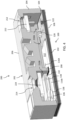
Figures 1 and 2 illustrating an exploded perspective view and assembled perspective view, respectively, of aportion 100 of an optical integrated circuit package. Reference is also made toFigure 3 which illustrates a partial cross sectional view of theportion 100 of the optical integrated circuit package taken along dottedline 3 inFigure 2 . Asupport substrate 102 is made of an insulating material (perhaps including multiple layers) and includes an upper surface and a lower surface. Thesupport substrate 102 may, for example, be of a printed circuit board (PCB) type. The upper surface ofsupport substrate 102 is covered by a firstsolder mask layer 104 including openings that expose upper circuit connection pads. The lower surface ofsupport substrate 102 is covered by a secondsolder mask layer 108 including openings that expose lower circuit pads. The upper circuit connection pads are electrically connected to the lower circuit pads through an electrical interconnection network (not explicitly shown) within thesupport substrate 102. - A lower (or back) surface of an optical sensor integrated circuit (IC) device (i.e., an IC die) 112 is mounted to the upper surface of the first
solder mask layer 104 andelectrical pads 120 of the optical sensorintegrated circuit device 112 are wirebonded to certain ones of the uppercircuit connection pads 121 located within corresponding opening(s) in the firstsolder mask layer 104. The optical sensorintegrated circuit device 112 includes, at its upper (or front) surface, a firstoptical sensor array 116A and a secondoptical sensor array 116B (i.e., a front-side illuminated sensor) supported by a semiconductor material substrate. Thearrays circuit device 112 may instead be surface mounted, in a flip-chip configuration, to certain ones of the upper circuit connection pads located within an opening in the firstsolder mask layer 104, with the firstoptical sensor array 116A and secondoptical sensor array 116B provided at a lower (or back) surface (i.e., a back-side illuminated sensor). - An optical emitter
integrated circuit device 122 is surface mounted to certain one(s) of the upper circuit connection pads within corresponding opening(s) in the firstsolder mask layer 104 and wirebonded to certain other one(s) of the upper circuit connection pads within corresponding opening(s) in the firstsolder mask layer 104. -
Auxiliary circuit components 128 are surface mounted to certain ones of the upper circuit connection pads within corresponding openings in the firstsolder mask layer 104. - The illustrated circuitry may, for example, form a time-of-flight sensing circuit where the optical emitter
integrated circuit device 122 is configured to emit a pulse of (infrared) light that is sensed by the firstoptical sensor array 116A of the optical sensorintegrated circuit device 112 to provide a reference time for light emission, with a target reflection of the emitted pulse of light being sensed by the secondoptical sensor array 116B of the optical sensorintegrated circuit device 112 to provide a detection time for light reflection. Distance from the optical integrated circuit package to the target may then be calculated as a function of the time difference between the reference time and the detection time. Power connections and signal connections for theportion 100 are provided through the lower circuit pads exposed by the openings in the secondsolder mask layer 108. - An
optical filter 132 is mounted to extend over the secondoptical sensor array 116B of the optical sensorintegrated circuit device 112. Theoptical filter 132 may, for example, be configured to selectively pass light within a certain range of wavelengths (for example, infrared) corresponding to a wavelength of the light emitted by the optical emitterintegrated circuit device 122. Theoptical filter 132 is configured as a flat rectangular plate that has, for example, a parallelpipedal shape (i.e., a six-faced polyhedron all of whose faces are parallelograms lying in pairs of parallel planes). The major (i.e., top and bottom) faces of the parallelpipedal-shapedoptical filter 132 extend in the x-y plane parallel to the upper surface of the optical sensorintegrated circuit device 112 and completely cover the secondoptical sensor array 116B. The minor (i.e., side or peripheral edge) faces of the parallelpipedal-shapedoptical filter 132 extend in the z-direction perpendicular to the upper surface of the optical sensorintegrated circuit device 112. - The mounting of the
optical filter 132 offset in the z-direction to the upper surface of the optical sensor integratedcircuit device 112 is accomplished using one or twodiscrete spacer blocks 136 andadhesive layers 138. In the embodiment of theportion 100 of the optical integrated circuit package shown inFigure 1 and 2 , a pair ofspacer blocks 136 are provided with one spacer block arranged to longitudinally extend (for example, in the x-direction) parallel to a first side edge of theoptical filter 132 and another spacer block arranged to longitudinally extend (for example, in the y-direction) parallel to a second side edge of the optical filter 132 (where the first and second side edges are adjacent each other). The spacer blocks 136, which have a thickness in the z-direction substantially equal to a desired z-direction offset of theoptical filter 132 from the upper surface of the optical sensor integratedcircuit device 112, are each made of a silicon material formed as a flat rectangular plate (having, for example, a parallelpipedal shape). The bottom surface of each spacer block is attached, for example using a layer of adhesive material (for example, comprising a die attach film (DAF) layer), to the upper surface of the optical sensor integratedcircuit device 112. The bottom surface of theoptical filter 132 is attached, for example using a layer of adhesive material (for example, comprising a die attach film (DAF) layer), to the upper surfaces of thespacer blocks 136. - The
spacer blocks 136 may, for example, be manufactured by singulating (i.e., dicing) a wafer of semiconductor (for example, silicon) material having a desired thickness in the z direction into desired sizes in the x-y plane. In an implementation, the semiconductor material of the wafer used to make the spacer blocks and the semiconductor substrate material of the optical sensor integratedcircuit device 112 are preferably a same semiconductor material (having identical coefficients of thermal expansion) or semiconductor materials have substantially similar coefficients of thermal expansion (for example, +/- 5% of each other). The diced portions of the wafer forming thespacer blocks 136 are then positioned, for example using a suitable pick-and-place manufacturing operation, at desired locations on the upper surface of the optical sensor integratedcircuit device 112. These desired locations may comprise, for example, free areas at the upper surface of the optical sensorintegrated circuit device 112 where neither the firstoptical sensor array 116A, nor the secondoptical sensor array 116B, nor theelectrical pads 120 of the optical sensorintegrated circuit device 112 are located. In particular, the free areas where thespacer blocks 136 are positioned for attachment may comprise areas along a side edge of the secondoptical sensor array 116B and/or between the side edge of the secondoptical sensor array 116B and the electrical pads of the optical sensor integratedcircuit device 112. Theadhesive material layers 138 may, for example, be provided at upper and lower surfaces of the wafer of semiconductor prior to singulation. - Likewise, the
optical filter 132 may, for example, be manufactured by singulating (i.e., dicing) a wafer of transparent (for example, glass) material having desired thickness in the z direction into desired sizes in the x-y plane. The diced portion of the wafer forming theoptical filter 132 is then positioned, for example using a suitable pick-and-place manufacturing operation, at a desired location on the spacer block (s) 136 and extending over at least the secondoptical sensor array 116B. - Suitable ultra-violet (UV) exposure may be used to activate and cure the adhesive material of the
layers 138 during manufacture of theportion 100. - It will be noted that at least one corner of the
optical filter 132, and perhaps two or more distal portions of side edges of theoptical filter 132, are not supported at all by aspacer block 136. That at least one corner and/or two or more distal portions of side edges of theoptical filter 132 extend unsupported, in a cantilever-like fashion, over the secondoptical sensor array 116B of the optical sensor integratedcircuit device 112. In the embodiment of theportion 100 of the optical integrated circuit package shown inFigure 1 and 2 , thecorner 150 and/or thedistal portions spacer blocks 136. - In particular: a first edge of the parallelpipedal-shaped
optical filter 132 is supported by thediscrete spacer block 136 and a second edge of the parallelpipedal-shapedoptical filter 132 opposite the first edge is not supported at all (see,Figure 5 , for example). Alternatively: a first corner of the parallelpipedal-shapedoptical filter 132 is supported by the discrete spacer block(s) 136 and a second corner of the parallelpipedal-shaped optical filter diagonally opposite the first corner is not supported at all by a spacer (see,Figure 2 , for example). In another implementation: the parallelpipedal-shapedoptical filter 132 includes a first edge and a second edge opposite the first edge of the parallelpipedal-shaped optical filter, with thediscrete spacer block 136 positioned between the first and second edges, and neither of the opposed first and second edges of the parallelpipedal-shapedoptical filter 132 is supported at all by a spacer. In yet another implementation: the parallelpipedal-shapedoptical filter 132 includes a first edge and a second edge adjacent the first edge, with onediscrete spacer block 136 positioned adjacent the first edge of the parallelpipedal-shaped optical filter, and anotherdiscrete spacer block 136 positioned adjacent the second edge of the parallelpipedal-shaped optical filter (see,Figure 2 , for example). In this case, it will be noted that a corner of the parallelpipedal-shapedoptical filter 132 diagonally opposite a corner at the adjacent first and second edges of the parallelpipedal-shapedoptical filter 132 is not supported at all by a spacer. - Reference is now made to
Figure 4 which illustrates a cross sectional perspective view of an opticalintegrated circuit package 200 including theportion 100 ofFigures 1 and 2 . Acap 202 is mounted to the upper surface of the firstsolder mask layer 104. The cap includesside walls 204, afront wall 206 over the side walls and apartition wall 208 extending between an opposed pair of side walls. Thepartition wall 208 is arranged to be placed between the firstoptical sensor array 116A and the secondoptical sensor array 116B of the optical sensor integratedcircuit device 112. Theside walls 204,front wall 206 andpartition wall 208 delimit two cavities within thecap 202. Thefirst cavity 210A includes the optical emitter integratedcircuit device 122 and a portion of the optical sensor integratedcircuit device 112 which includes the firstoptical sensor array 116A. Thesecond cavity 210B includes a portion of the optical sensor integratedcircuit device 112 which includes the secondoptical sensor array 116B. Thepartition wall 208 provides a light barrier for blocking light emitted by the optical emitter integratedcircuit device 122 from directly reaching the secondoptical sensor array 116B (in other words, the emitted light is block from propagating within the confines of thecap 202 to reach the secondoptical sensor array 116B) . It will be noted that light emitted by the optical emitter integratedcircuit device 122 can still directly reach the firstoptical sensor array 116A by propagating within the first cavity of thecap 202. Thefront wall 206 includes afirst opening 212 aligned with the optical emitter integratedcircuit device 122 and asecond opening 214 aligned with the secondoptical sensor array 116B. A first diffractive optical element 222 (for example, a lens) is mounted at and/or within thefirst opening 212. Light emitted by the optical emitter integratedcircuit device 122 passes through thefirst opening 212 and is directed by the first diffractiveoptical element 222 to illuminate a scene. A second diffractive optical element 224 (for example, a lens) is mounted at and/or within thesecond opening 214. Light reflected by an object in the illuminated scene passes through thesecond opening 214, is collected by the second diffractiveoptical element 224 and passes through the optical filter 134 to reach the secondoptical sensor array 116B. - While
Figures 1-4 show an implementation using a pair of spacer blocks 136 supporting adjacent sides of theoptical filter 132, it will be noted that alternative implementations as shown inFigures 5 and 6 may instead utilize just asingle spacer block 136. In theFigure 5 implementation, thespacer block 136 is provided at one end of the optical filter along a side edge with theoptical filter 132 extending in a cantilever over the secondoptical sensor array 116B. Note here that the side edge of theoptical filter 132 opposite to that where thespacer block 136 is attached is freely suspended with theadjacent corners 150 and/or thedistal portions spacer block 136. In theFigure 6 implementation, thespacer block 136 is provided at a location between opposite ends of the optical filter extending between opposed side edges. Each of the opposite ends of theoptical filter 132 extends in a cantilever from the supportingspacer block 136 with one end extending over the firstoptical sensor array 116A and another end extending over the secondoptical sensor array 116B. Note here that the opposite side edges of theoptical filter 132 between which thespacer block 136 is attached are freely suspended with theadjacent corners 150 and/or thedistal portions spacer block 136. - A number of advantages accrue from the use of the configuration for the
portion 100 as described above inFigures 1-6 , including: a) a reduction in cost of the assembly comprising theportion 100; b) support for an optical sensor integratedcircuit device 112 having a smaller dimension (since the spacer block(s) 136 can be selectively attached at open/free surface areas on the upper surface of the die); c) support for a secondoptical sensor array 116B of the optical sensor integratedcircuit device 112 having a larger dimension (since the spacer block(s) 136 can be selectively attached at open/free surface areas on the upper surface of the die offset from thearrays portion 100, and hence theoverall package 200, having a smaller dimension (since the spacer structure supporting theoptical filter 132 need not completely surround the secondoptical sensor array 116B of the optical sensor integrated circuit device 112); and e) reduction in thermal stress applied to the optical sensor integrated circuit device 112 (since coefficients of thermal expansion for the semiconductor material of the spacer block(s) 136 and the semiconductor substrate material of the optical sensor integratedcircuit device 112 can be identical or substantially matched). - All or part of the disclosed embodiments can be summarized by the following examples.
- Example 1: A device, comprising:
- a support substrate;
- an optical integrated circuit device mounted over an upper surface of the support substrate;
- wherein said optical integrated circuit device includes an optical sensor array supported by a semiconductor substrate made of a first semiconductor material;
- a first discrete semiconductor block made of a second semiconductor material;
- wherein the first and second semiconductor materials have substantially matched coefficients of thermal expansion;
- wherein the first discrete semiconductor block is mounted over an upper surface of the optical integrated circuit device adjacent the optical sensor array; and
- a parallelpipedal-shaped optical filter mounted over an upper surface of the first discrete semiconductor block and extending over the optical sensor array.
- Example 2: The device of example 1, wherein the first and second semiconductor materials are a same semiconductor material.
- Example 3: The device of example 2, wherein said same semiconductor material is silicon.
- Example 4: The device of any of examples 1 to 3, wherein a first edge of the parallelpipedal-shaped optical filter is supported by the first discrete semiconductor block and a second edge of the parallelpipedal-shaped optical filter opposite the first edge is not supported at all.
- Example 5: The device of any of examples 1 to 3, wherein a first corner of the parallelpipedal-shaped optical filter is supported by the first discrete semiconductor block and a second corner of the parallelpipedal-shaped optical filter opposite the first corner is not supported at all.
- Example 6: The device of any of examples 1 to 3, wherein the parallelpipedal-shaped optical filter includes a first edge and a second edge opposite the first edge of the parallelpipedal-shaped optical filter, and wherein the first discrete semiconductor block is positioned between the first and second edges, and wherein neither of the first and second edges of the parallelpipedal-shaped optical filter is supported at all.
- Example 7: The device of example 6, wherein said optical integrated circuit device further includes a further optical sensor array, and wherein said first discrete semiconductor block is positioned between the optical sensor array and the further optical sensor array.
- Example 8: The device of example 7, wherein the parallelpipedal-shaped optical filter at said first edge extends over the optical sensor array, and wherein the parallelpipedal-shaped optical filter at said second edge extends over the further optical sensor array.
- Example 9: The device of any of examples 1 to 3, wherein the parallelpipedal-shaped optical filter is supported solely by said first discrete semiconductor block.
- Example 10: The device of example 9, wherein a first edge of the parallelpipedal-shaped optical filter is supported by the first discrete semiconductor block and a second edge of the parallelpipedal-shaped optical filter opposite the first edge is not supported at all.
- Example 11: The device of any of examples 1 to 3, further comprising a second discrete semiconductor block made of the second semiconductor material, and wherein the parallelpipedal-shaped optical filter is mounted over an upper surface of the second discrete semiconductor block.
- Example 12: The device of example 11, wherein the parallelpipedal-shaped optical filter includes a first edge and a second edge adjacent the first edge of the parallelpipedal-shaped optical filter, and wherein the first discrete semiconductor block is positioned adjacent the first edge of the parallelpipedal-shaped optical filter, and wherein the second discrete semiconductor block is positioned adjacent the second edge of the parallelpipedal-shaped optical filter.
- Example 13: The device of example 12, wherein a corner of the parallelpipedal-shaped optical filter opposite a corner at the adjacent first and second edges of the parallelpipedal-shaped optical filter is not supported at all.
- Example 14: The device of any of examples 1 to 13, further comprising:
- a first adhesive layer between the first discrete semiconductor block and the upper surface of the optical integrated circuit device; and
- a second adhesive layer between the parallelpipedal-shaped optical filter and the upper surface of the first discrete semiconductor block.
- Example 15: The device of example 14, wherein at least one of the first and second adhesive layers is formed by a die attach film (DAF) layer.
- Example 16: The device of any of examples 1 to 15, further comprising a cap mounted over the upper surface of the support substrate, said cap including walls delimiting a cavity within which the optical sensor array and at least part of said optical integrated circuit device is located, said cap including a wall opening aligned with the optical sensor array.
- Example 17: The device of example 16, further comprising a diffractive optical element mounted at said wall opening.
- Example 18: The device of any of examples 1 to 17, wherein said support substrate comprises a printed circuit board (PCB) including circuit connection pads that are electrically connected to electrical connection pads of the optical integrated circuit device.
- While the invention has been illustrated and described in detail in the drawings and foregoing description, such illustration and description are considered illustrative or exemplary and not restrictive; the invention is not limited to the disclosed embodiments. Other variations to the disclosed embodiments can be understood and effected by those skilled in the art in practicing the claimed invention, from a study of the drawings, the disclosure, and the appended claims.
Claims (16)
- A device, comprising:a support substrate;an optical integrated circuit device mounted over an upper surface of the support substrate;wherein said optical integrated circuit device includes an optical sensor array supported by a semiconductor substrate made of a first semiconductor material;a first discrete semiconductor block made of a second semiconductor material;wherein the first and second semiconductor materials have substantially matched coefficients of thermal expansion; wherein the first discrete semiconductor block is mounted over an upper surface of the optical integrated circuit device adjacent the optical sensor array; anda parallelpipedal-shaped optical filter mounted over an upper surface of the first discrete semiconductor block and extending over the optical sensor array.
- The device of claim 1, wherein the first and second semiconductor materials are a same semiconductor material, preferably silicon.
- The device of claim 1 or 2, wherein a first corner of the parallelpipedal-shaped optical filter is supported by the first discrete semiconductor block and a second corner of the parallelpipedal-shaped optical filter opposite the first corner is not supported at all.
- The device of any of claims 1 to 3, wherein a first edge of the parallelpipedal-shaped optical filter is supported by the first discrete semiconductor block and a second edge of the parallelpipedal-shaped optical filter opposite the first edge is not supported at all.
- The device of any of claims 1 to 3, wherein the parallelpipedal-shaped optical filter includes a first edge and a second edge opposite the first edge of the parallelpipedal-shaped optical filter, and wherein the first discrete semiconductor block is positioned between the first and second edges, and wherein neither of the first and second edges of the parallelpipedal-shaped optical filter is supported at all.
- The device of claim 5, wherein said optical integrated circuit device further includes a further optical sensor array, and wherein said first discrete semiconductor block is positioned between the optical sensor array and the further optical sensor array.
- The device of claim 6, wherein the parallelpipedal-shaped optical filter at said first edge extends over the optical sensor array, and wherein the parallelpipedal-shaped optical filter at said second edge extends over the further optical sensor array.
- The device of any of claims 1 to 7, wherein the parallelpipedal-shaped optical filter is supported solely by said first discrete semiconductor block.
- The device of any of claims 1 to 3, further comprising a second discrete semiconductor block made of the second semiconductor material, and wherein the parallelpipedal-shaped optical filter mounted over an upper surface of the second discrete semiconductor block.
- The device of claim 9, wherein the parallelpipedal-shaped optical filter includes a first edge and a second edge adjacent the first edge of the parallelpipedal-shaped optical filter, and wherein the first discrete semiconductor block is positioned adjacent the first edge of the parallelpipedal-shaped optical filter, and wherein the second discrete semiconductor block is positioned adjacent the second edge of the parallelpipedal-shaped optical filter.
- The device of claim 10, wherein a corner of the parallelpipedal-shaped optical filter opposite a corner at the adjacent first and second edges of the parallelpipedal-shaped optical filter is not supported at all.
- The device of any of claims 1 to 11, further comprising:a first adhesive layer between the first discrete semiconductor block and the upper surface of the optical integrated circuit device; anda second adhesive layer between the parallelpipedal-shaped optical filter and the upper surface of the first discrete semiconductor block.
- The device of claim 12, wherein at least one of the first and second adhesive layers is formed by a die attach film (DAF) layer.
- The device of any of claims 1 to 13, further comprising a cap mounted over the upper surface of the support substrate, said cap including walls delimiting a cavity within which the optical sensor array and at least part of said optical integrated circuit device is located, said cap including a wall opening aligned with the optical sensor array.
- The device of claim 14, further comprising a diffractive optical element mounted at said wall opening.
- The device of any of claims 1 to 15, wherein said support substrate comprises a printed circuit board (PCB) including circuit connection pads that are electrically connected to electrical connection pads of the optical integrated circuit device.
Applications Claiming Priority (1)
| Application Number | Priority Date | Filing Date | Title |
|---|---|---|---|
| US18/133,299 US12189064B2 (en) | 2023-04-11 | 2023-04-11 | Stacked filter assembly for optical integrated circuit package with an optical filter mounted to an optical integrated circuit device by a discrete semiconductor spacer block |
Publications (1)
| Publication Number | Publication Date |
|---|---|
| EP4447472A1 true EP4447472A1 (en) | 2024-10-16 |
Family
ID=90719282
Family Applications (1)
| Application Number | Title | Priority Date | Filing Date |
|---|---|---|---|
| EP24169015.5A Pending EP4447472A1 (en) | 2023-04-11 | 2024-04-08 | Stacked filter assembly for optical integrated circuit package with an optical filter mounted to an optical integrated circuit device by a discrete semiconductor spacer block |
Country Status (3)
| Country | Link |
|---|---|
| US (1) | US12189064B2 (en) |
| EP (1) | EP4447472A1 (en) |
| CN (1) | CN118795599A (en) |
Citations (3)
| Publication number | Priority date | Publication date | Assignee | Title |
|---|---|---|---|---|
| EP1536478A2 (en) * | 2003-11-25 | 2005-06-01 | Fuji Photo Film Co., Ltd. | Solid state imaging device and producing method thereof |
| WO2007077752A1 (en) * | 2005-12-27 | 2007-07-12 | Sumitomo Electric Industries, Ltd. | Semiconductor element mounting member, fabrication method thereof, and semiconductor device |
| US20140124733A1 (en) * | 2009-09-15 | 2014-05-08 | Showa Denko K.K. | Light emitting diode, light emitting diode lamp, and illuminating apparatus |
Family Cites Families (8)
| Publication number | Priority date | Publication date | Assignee | Title |
|---|---|---|---|---|
| US20040135473A1 (en) * | 2003-01-15 | 2004-07-15 | Byers Charles L. | Piezoelectric devices mounted on integrated circuit chip |
| US20130175650A1 (en) | 2012-01-05 | 2013-07-11 | Apple Inc | Cover for image sensor assembly with light absorbing layer |
| KR102273850B1 (en) * | 2013-10-31 | 2021-07-05 | 하마마츠 포토닉스 가부시키가이샤 | Light-detecting device |
| US9228894B2 (en) | 2014-04-14 | 2016-01-05 | Teledyne Scientific & Imaging, Llc | Optical sensor and filter assembly with epoxy mounting structure and method of assembly |
| JP6631255B2 (en) * | 2016-01-08 | 2020-01-15 | セイコーエプソン株式会社 | Oscillation module, electronic device, and moving object |
| US9793427B1 (en) * | 2016-07-25 | 2017-10-17 | Stmicroelectronics Pte Ltd | Air venting on proximity sensor |
| KR20200142366A (en) * | 2019-06-12 | 2020-12-22 | 삼성전기주식회사 | Image sensor package |
| KR102494691B1 (en) | 2020-09-11 | 2023-02-02 | 주식회사 옵트론텍 | Optical filter carrier, image sensor package having optical filter, and method of fabricating the same |
-
2023
- 2023-04-11 US US18/133,299 patent/US12189064B2/en active Active
-
2024
- 2024-04-08 CN CN202410413494.XA patent/CN118795599A/en active Pending
- 2024-04-08 EP EP24169015.5A patent/EP4447472A1/en active Pending
Patent Citations (3)
| Publication number | Priority date | Publication date | Assignee | Title |
|---|---|---|---|---|
| EP1536478A2 (en) * | 2003-11-25 | 2005-06-01 | Fuji Photo Film Co., Ltd. | Solid state imaging device and producing method thereof |
| WO2007077752A1 (en) * | 2005-12-27 | 2007-07-12 | Sumitomo Electric Industries, Ltd. | Semiconductor element mounting member, fabrication method thereof, and semiconductor device |
| US20140124733A1 (en) * | 2009-09-15 | 2014-05-08 | Showa Denko K.K. | Light emitting diode, light emitting diode lamp, and illuminating apparatus |
Also Published As
| Publication number | Publication date |
|---|---|
| CN118795599A (en) | 2024-10-18 |
| US12189064B2 (en) | 2025-01-07 |
| US20240345229A1 (en) | 2024-10-17 |
Similar Documents
| Publication | Publication Date | Title |
|---|---|---|
| US8092734B2 (en) | Covers for microelectronic imagers and methods for wafer-level packaging of microelectronics imagers | |
| JP5063839B2 (en) | Manufacturing method of chip mount type sealing structure | |
| JP3507251B2 (en) | Optical sensor IC package and method of assembling the same | |
| US20070126912A1 (en) | Camera module and manufacturing method for such a camera module | |
| CN113161318A (en) | Sensor package | |
| US11462500B2 (en) | Optoelectronic semiconductor device and method for producing optoelectronic semiconductor devices | |
| US11264778B2 (en) | Quad flat no-leads package for side emitting laser diode | |
| KR200489765Y1 (en) | Sensor module | |
| JP2004193600A (en) | Semiconductor device and method of manufacturing the same, cover for semiconductor device, and electronic device | |
| US12189064B2 (en) | Stacked filter assembly for optical integrated circuit package with an optical filter mounted to an optical integrated circuit device by a discrete semiconductor spacer block | |
| JP2008113039A (en) | Method for manufacturing light emitting device | |
| JP5010198B2 (en) | Light emitting device | |
| WO2024080297A1 (en) | Photodetector | |
| WO2014014415A1 (en) | Compact spectrometer module and method for manufacturing the same | |
| TWI785195B (en) | Semiconductor device | |
| EP3754798B1 (en) | Multipiece element storage package, and multipiece optical semiconductor device | |
| JP2009177101A (en) | Light emitting device | |
| JP2009177099A (en) | Light emitting device | |
| WO2014014412A1 (en) | Compact optical module and method for manufacturing the same | |
| CN114300932B (en) | Chip packaging structure, forming method and electronic device | |
| JP5351620B2 (en) | Light emitting device | |
| JP2020088309A (en) | Optical module package and manufacturing method of the same | |
| JP5102640B2 (en) | Light emitting device | |
| CN117878164A (en) | Light sensing chip, light sensing module and laser radar | |
| HK1196181A (en) | Low profile image sensor package and method |
Legal Events
| Date | Code | Title | Description |
|---|---|---|---|
| PUAI | Public reference made under article 153(3) epc to a published international application that has entered the european phase |
Free format text: ORIGINAL CODE: 0009012 |
|
| STAA | Information on the status of an ep patent application or granted ep patent |
Free format text: STATUS: REQUEST FOR EXAMINATION WAS MADE |
|
| 17P | Request for examination filed |
Effective date: 20240408 |
|
| AK | Designated contracting states |
Kind code of ref document: A1 Designated state(s): AL AT BE BG CH CY CZ DE DK EE ES FI FR GB GR HR HU IE IS IT LI LT LU LV MC ME MK MT NL NO PL PT RO RS SE SI SK SM TR |
|
| GRAP | Despatch of communication of intention to grant a patent |
Free format text: ORIGINAL CODE: EPIDOSNIGR1 |
|
| STAA | Information on the status of an ep patent application or granted ep patent |
Free format text: STATUS: GRANT OF PATENT IS INTENDED |
|
| RIC1 | Information provided on ipc code assigned before grant |
Ipc: H04N 23/55 20230101AFI20260115BHEP |
|
| INTG | Intention to grant announced |
Effective date: 20260203 |