EP4446809A2 - Verfahren zur bewertung einer auf einem euv-maskenrohling geformten referenzmarkierung - Google Patents
Verfahren zur bewertung einer auf einem euv-maskenrohling geformten referenzmarkierung Download PDFInfo
- Publication number
- EP4446809A2 EP4446809A2 EP24167570.1A EP24167570A EP4446809A2 EP 4446809 A2 EP4446809 A2 EP 4446809A2 EP 24167570 A EP24167570 A EP 24167570A EP 4446809 A2 EP4446809 A2 EP 4446809A2
- Authority
- EP
- European Patent Office
- Prior art keywords
- reference mark
- contrast
- mask blank
- euv mask
- evaluation
- Prior art date
- Legal status (The legal status is an assumption and is not a legal conclusion. Google has not performed a legal analysis and makes no representation as to the accuracy of the status listed.)
- Pending
Links
Images

Classifications
-
- G—PHYSICS
- G03—PHOTOGRAPHY; CINEMATOGRAPHY; ANALOGOUS TECHNIQUES USING WAVES OTHER THAN OPTICAL WAVES; ELECTROGRAPHY; HOLOGRAPHY
- G03F—PHOTOMECHANICAL PRODUCTION OF TEXTURED OR PATTERNED SURFACES, e.g. FOR PRINTING, FOR PROCESSING OF SEMICONDUCTOR DEVICES; MATERIALS THEREFOR; ORIGINALS THEREFOR; APPARATUS SPECIALLY ADAPTED THEREFOR
- G03F1/00—Originals for photomechanical production of textured or patterned surfaces, e.g., masks, photo-masks, reticles; Mask blanks or pellicles therefor; Containers specially adapted therefor; Preparation thereof
- G03F1/52—Reflectors
-
- G—PHYSICS
- G03—PHOTOGRAPHY; CINEMATOGRAPHY; ANALOGOUS TECHNIQUES USING WAVES OTHER THAN OPTICAL WAVES; ELECTROGRAPHY; HOLOGRAPHY
- G03F—PHOTOMECHANICAL PRODUCTION OF TEXTURED OR PATTERNED SURFACES, e.g. FOR PRINTING, FOR PROCESSING OF SEMICONDUCTOR DEVICES; MATERIALS THEREFOR; ORIGINALS THEREFOR; APPARATUS SPECIALLY ADAPTED THEREFOR
- G03F1/00—Originals for photomechanical production of textured or patterned surfaces, e.g., masks, photo-masks, reticles; Mask blanks or pellicles therefor; Containers specially adapted therefor; Preparation thereof
- G03F1/22—Masks or mask blanks for imaging by radiation of 100nm or shorter wavelength, e.g. X-ray masks, extreme ultraviolet [EUV] masks; Preparation thereof
- G03F1/24—Reflection masks; Preparation thereof
-
- G—PHYSICS
- G03—PHOTOGRAPHY; CINEMATOGRAPHY; ANALOGOUS TECHNIQUES USING WAVES OTHER THAN OPTICAL WAVES; ELECTROGRAPHY; HOLOGRAPHY
- G03F—PHOTOMECHANICAL PRODUCTION OF TEXTURED OR PATTERNED SURFACES, e.g. FOR PRINTING, FOR PROCESSING OF SEMICONDUCTOR DEVICES; MATERIALS THEREFOR; ORIGINALS THEREFOR; APPARATUS SPECIALLY ADAPTED THEREFOR
- G03F1/00—Originals for photomechanical production of textured or patterned surfaces, e.g., masks, photo-masks, reticles; Mask blanks or pellicles therefor; Containers specially adapted therefor; Preparation thereof
- G03F1/38—Masks having auxiliary features, e.g. special coatings or marks for alignment or testing; Preparation thereof
-
- G—PHYSICS
- G03—PHOTOGRAPHY; CINEMATOGRAPHY; ANALOGOUS TECHNIQUES USING WAVES OTHER THAN OPTICAL WAVES; ELECTROGRAPHY; HOLOGRAPHY
- G03F—PHOTOMECHANICAL PRODUCTION OF TEXTURED OR PATTERNED SURFACES, e.g. FOR PRINTING, FOR PROCESSING OF SEMICONDUCTOR DEVICES; MATERIALS THEREFOR; ORIGINALS THEREFOR; APPARATUS SPECIALLY ADAPTED THEREFOR
- G03F1/00—Originals for photomechanical production of textured or patterned surfaces, e.g., masks, photo-masks, reticles; Mask blanks or pellicles therefor; Containers specially adapted therefor; Preparation thereof
- G03F1/38—Masks having auxiliary features, e.g. special coatings or marks for alignment or testing; Preparation thereof
- G03F1/42—Alignment or registration features, e.g. alignment marks on the mask substrates
-
- G—PHYSICS
- G03—PHOTOGRAPHY; CINEMATOGRAPHY; ANALOGOUS TECHNIQUES USING WAVES OTHER THAN OPTICAL WAVES; ELECTROGRAPHY; HOLOGRAPHY
- G03F—PHOTOMECHANICAL PRODUCTION OF TEXTURED OR PATTERNED SURFACES, e.g. FOR PRINTING, FOR PROCESSING OF SEMICONDUCTOR DEVICES; MATERIALS THEREFOR; ORIGINALS THEREFOR; APPARATUS SPECIALLY ADAPTED THEREFOR
- G03F1/00—Originals for photomechanical production of textured or patterned surfaces, e.g., masks, photo-masks, reticles; Mask blanks or pellicles therefor; Containers specially adapted therefor; Preparation thereof
- G03F1/38—Masks having auxiliary features, e.g. special coatings or marks for alignment or testing; Preparation thereof
- G03F1/44—Testing or measuring features, e.g. grid patterns, focus monitors, sawtooth scales or notched scales
-
- G—PHYSICS
- G03—PHOTOGRAPHY; CINEMATOGRAPHY; ANALOGOUS TECHNIQUES USING WAVES OTHER THAN OPTICAL WAVES; ELECTROGRAPHY; HOLOGRAPHY
- G03F—PHOTOMECHANICAL PRODUCTION OF TEXTURED OR PATTERNED SURFACES, e.g. FOR PRINTING, FOR PROCESSING OF SEMICONDUCTOR DEVICES; MATERIALS THEREFOR; ORIGINALS THEREFOR; APPARATUS SPECIALLY ADAPTED THEREFOR
- G03F1/00—Originals for photomechanical production of textured or patterned surfaces, e.g., masks, photo-masks, reticles; Mask blanks or pellicles therefor; Containers specially adapted therefor; Preparation thereof
- G03F1/68—Preparation processes not covered by groups G03F1/20 - G03F1/50
- G03F1/82—Auxiliary processes, e.g. cleaning or inspecting
- G03F1/84—Inspecting
-
- G—PHYSICS
- G03—PHOTOGRAPHY; CINEMATOGRAPHY; ANALOGOUS TECHNIQUES USING WAVES OTHER THAN OPTICAL WAVES; ELECTROGRAPHY; HOLOGRAPHY
- G03F—PHOTOMECHANICAL PRODUCTION OF TEXTURED OR PATTERNED SURFACES, e.g. FOR PRINTING, FOR PROCESSING OF SEMICONDUCTOR DEVICES; MATERIALS THEREFOR; ORIGINALS THEREFOR; APPARATUS SPECIALLY ADAPTED THEREFOR
- G03F7/00—Photomechanical, e.g. photolithographic, production of textured or patterned surfaces, e.g. printing surfaces; Materials therefor, e.g. comprising photoresists; Apparatus specially adapted therefor
- G03F7/70—Microphotolithographic exposure; Apparatus therefor
- G03F7/70008—Production of exposure light, i.e. light sources
- G03F7/70033—Production of exposure light, i.e. light sources by plasma extreme ultraviolet [EUV] sources
-
- G—PHYSICS
- G03—PHOTOGRAPHY; CINEMATOGRAPHY; ANALOGOUS TECHNIQUES USING WAVES OTHER THAN OPTICAL WAVES; ELECTROGRAPHY; HOLOGRAPHY
- G03F—PHOTOMECHANICAL PRODUCTION OF TEXTURED OR PATTERNED SURFACES, e.g. FOR PRINTING, FOR PROCESSING OF SEMICONDUCTOR DEVICES; MATERIALS THEREFOR; ORIGINALS THEREFOR; APPARATUS SPECIALLY ADAPTED THEREFOR
- G03F7/00—Photomechanical, e.g. photolithographic, production of textured or patterned surfaces, e.g. printing surfaces; Materials therefor, e.g. comprising photoresists; Apparatus specially adapted therefor
- G03F7/70—Microphotolithographic exposure; Apparatus therefor
- G03F7/70483—Information management; Active and passive control; Testing; Wafer monitoring, e.g. pattern monitoring
- G03F7/70605—Workpiece metrology
- G03F7/70681—Metrology strategies
- G03F7/70683—Mark designs
-
- G—PHYSICS
- G03—PHOTOGRAPHY; CINEMATOGRAPHY; ANALOGOUS TECHNIQUES USING WAVES OTHER THAN OPTICAL WAVES; ELECTROGRAPHY; HOLOGRAPHY
- G03F—PHOTOMECHANICAL PRODUCTION OF TEXTURED OR PATTERNED SURFACES, e.g. FOR PRINTING, FOR PROCESSING OF SEMICONDUCTOR DEVICES; MATERIALS THEREFOR; ORIGINALS THEREFOR; APPARATUS SPECIALLY ADAPTED THEREFOR
- G03F9/00—Registration or positioning of originals, masks, frames, photographic sheets or textured or patterned surfaces, e.g. automatically
- G03F9/70—Registration or positioning of originals, masks, frames, photographic sheets or textured or patterned surfaces, e.g. automatically for microlithography
- G03F9/7088—Alignment mark detection, e.g. TTR, TTL, off-axis detection, array detector, video detection
-
- G—PHYSICS
- G06—COMPUTING OR CALCULATING; COUNTING
- G06T—IMAGE DATA PROCESSING OR GENERATION, IN GENERAL
- G06T7/00—Image analysis
- G06T7/0002—Inspection of images, e.g. flaw detection
- G06T7/0004—Industrial image inspection
- G06T7/001—Industrial image inspection using an image reference approach
-
- G—PHYSICS
- G06—COMPUTING OR CALCULATING; COUNTING
- G06T—IMAGE DATA PROCESSING OR GENERATION, IN GENERAL
- G06T2207/00—Indexing scheme for image analysis or image enhancement
- G06T2207/30—Subject of image; Context of image processing
- G06T2207/30108—Industrial image inspection
- G06T2207/30148—Semiconductor; IC; Wafer
Definitions
- the present invention relates to a method for evaluating a reference mark formed on a reflective mask blank for reflecting EUV light (EUV mask blank) used in manufacturing a semiconductor device, etc.
- Semiconductor devices are manufactured by using photolithography technology in which a mask for transferring a pattern, such as a photomask with a drawn circuit pattern, is irradiated with exposure light to transfer the circuit pattern formed on the mask onto a semiconductor substrate via a reduction optical system.
- a wavelength of the exposure light has been mainly 193 nm using argon fluoride (ArF) excimer laser light, and adopting a process "multi-patterning" of combining exposure processes and processing processes a plurality of times can form a sufficiently small-sized pattern compared with the exposure light wavelength.
- ArF argon fluoride
- the EUV light is light having a wavelength of near 13.5 nm. Since the conventional transmission projection optical system and mask cannot be used for this EUV light, reflective optical elements are used.
- a reflective mask is also proposed for a mask for transferring a pattern.
- a multilayer reflective film to reflect EUV light is formed on a substrate, and an absorber film to absorb EUV light is patterned on the multilayer reflective film. Meanwhile, a state before the pattern is formed on the absorber film (including a state where a resist layer is formed) is called as a reflective mask blank, which is used as a material for the reflective mask.
- the reflective mask blank for reflecting EUV light is also referred to as "EUV mask blank”.
- the EUV mask blank has a basic structure having: the multilayer reflective film formed on a low thermal-expansion substrate to reflect EUV light; and the absorber film formed thereon to absorb EUV light.
- the multilayer reflective film is a Mo/Si multilayer reflective film in which molybdenum (Mo) films and silicon (Si) films are alternately stacked to achieve reflectance of EUV light.
- a protective film for protecting the multilayer reflective film is formed.
- the absorber film a material mainly composed of tantalum (Ta) and chromium (Cr), which has a relatively large value of an extinction coefficient against EUV light, is used.
- Patent Document 1 discloses art of forming a reference mark on the absorber film, recognizing a position of the phase defect on the multilayer reflective film as a position of roughness on the surface of the absorber film thereon to convert the position into defect position information relative to the reference mark, and modifying a drawing data for pattering of the absorber film based on the defect position information to avoid the position of the phase defect and perform patterning of the absorber film.
- structure turbulence of the multilayer reflective film to decrease the reflectance may be hardly exhibited as the roughness on the surface of the multilayer reflective film, and it is difficult to accurately obtain the positional information of all phase defects in inspection of the absorber film.
- Patent Document 3 discloses a method using a dark-field inspection image, for example.
- a reference mark on the EUV mask blank is an indicator for accurately defining the defect position, and thereby processing accuracy of the reference mark is an important quality parameter. For example, a case where the reference mark cannot be detected with an inspection apparatus due to considerable shift of the position of the reference mark from the designed position, etc. can be judged as processing failure of the reference mark.
- the reference mark may be produced with a shallower depth than the design even when the reference mark is normally detected with an inspection apparatus, and such a defective product causes unevenness of detection sensitivity with the inspection apparatus. If such a defective product is shipped, the reference mark cannot be detected with an apparatus in a customer's process, which may cause quality failure.
- the processing accuracy of the reference mark is required to be evaluated, and can be measured by using an atomic force microscope (AFM) as the evaluation method, for example.
- AFM atomic force microscope
- the AFM measurement is destructive inspection, and the substrate itself used for producing the mask cannot be measured.
- An object of the present invention is to provide an EUV mask blank evaluation method that can easily evaluate processing accuracy of the reference mark (for example, depth).
- the present invention provides a method for evaluating a reference mark formed on an EUV mask blank, the method comprising steps of:
- the present inventors have made earnest study, and found that the reference mark contrast ⁇ (hereinafter, also simply referred to as "contrast ⁇ ") has correlation with the processing accuracy (for example, depth) of the reference mark, and the processing accuracy of the reference mark can be evaluated by measuring the contrast ⁇ .
- the present invention is a method for evaluating the EUV mask blank with this novel indicator, and the processing accuracy of the reference mark can be easily evaluated without destruction.
- the evaluation method of the present invention enables total inspection without increasing a time of the evaluation step by simultaneously performing the method with defect inspection, for example.
- the evaluation method of the present invention can eliminate products with abnormal processing accuracy of the reference mark to provide high-quality products.
- Evaluating the processing accuracy of the reference mark may comprise:
- Such a method can more accurately evaluate the depth-processing accuracy of the reference mark, and can judge its quality (normality or abnormality) to determine good products among evaluation-target EUV mask blanks. This can more certainly provide the EUV mask blanks with stable quality.
- Evaluating the processing accuracy of the reference mark may comprise:
- This method can also more accurately evaluate the depth-processing accuracy of the reference mark, and can judge its quality (normality or abnormality) to determine good products among evaluation-target EUV mask blanks. This can more certainly provide the EUV mask blanks with stable quality.
- the reference mark In imaging the reference mark formed on the EUV mask blank to obtain the reference mark image, the reference mark may be imaged with a Schwarzschild optical system and with a dark-field inspection image.
- the reference mark is suitably imaged with a Schwarzschild optical system and with a dark-field inspection image.
- a reference mark contrast is applied as an indicator for evaluating processing accuracy of a reference mark on an EUV mask blank.
- the evaluation method of the present invention comprises steps of: imaging the reference mark formed on the EUV mask blank to obtain a reference mark image; obtaining a reference mark contrast (contrast between the reference mark and the background level) from the obtained reference mark image; and evaluating processing accuracy of the reference mark on the EUV mask blank with the obtained reference mark contrast.
- the reference EUV mask blank with the varied depth of the reference mark is prepared as above.
- the number of the depth condition is one or more, but a plurality of the numbers is particularly preferable.
- the upper limit of the number is not particularly limited, and may be five to ten, for example.
- One reference EUV mask blank on which the plurality of the reference marks having different depths is formed may be prepared, or a plurality of same reference EUV mask blanks on which one reference mark having a different depth is each formed may be prepared.
- the reference mark on the reference EUV mask blank is imaged to obtain a reference mark image.
- Any apparatus that can perform imaging to obtain the reference mark contrast later from the obtained image may be used, and a defect inspection apparatus that can obtain a defect image may be used, for example. It is particularly preferable to obtain a dark-field inspection image with a Schwarzschild optical system, but the method is not particularly limited.
- the imaging conditions a state where defects such as a foreign matter, a dimple, and a pinhole are absent in the image field including the reference mark is preferable because furthermore accurate evaluation can be performed.
- a wavelength used for the imaging is not particularly limited as long as the reference mark image and the reference mark contrast can be obtained.
- the wavelength is preferably 600 nm or shorter, for example.
- the lower limit is not particularly limited, and the light may also be EUV light (approximately 1 nm to 100 nm, particularly around 13.5 nm), for example.
- each of the reference mark contrast is obtained. This is used as the reference contrast.
- an image in which a difference in light intensity, etc. is emphasized by using an image-processing algorithm such as differential processing may be used as necessary.
- the obtained evaluation-target contrast is compared with the reference contrast for evaluating processing accuracy of the reference mark formed on the evaluation-target EUV mask blank to judge quality of the reference mark.
- the criteria of the comparative evaluation here are not particularly limited.
- the comparison may be performed with the obtained reference contrast itself, or criteria set based on the obtained reference contrast may be used.
- a target contrast is set with reference to the reference contrast, and criteria within ⁇ 10% of the target contrast may be set as a normal value (good product).
- a lower detection limit contrast of the apparatus is evaluated and determined from the reference contrast obtained by evaluating the reference marks having different depths on the aforementioned reference EUV mask blank, and a case of the lower detection limit contrast or higher may also be set as a normal value (good product).
- quality of the reference mark formed on the EUV mask blank can be managed.
- Such criteria can more certainly judge a reference mark with abnormal depth-processing accuracy among normal reference marks, and quality of the evaluation target can be judged with further higher accuracy.
- stabilization of the quality of the EUV mask blank can be more certainly achieved.
- criteria are not limited to the above “within ⁇ 10%”, and a numerical range (threshold) being criteria may be set depending on desired evaluation criteria.
- processing accuracy, such as depth, of the reference mark formed on the EUV mask blank can be easily evaluated without destruction, which differs from the conventional destructive inspection using an AFM, for example.
- obtaining the reference mark image in defect inspection can efficiently perform total inspection.
- simultaneously performing the evaluation method of the present invention enables the total inspection without increasing a time of the evaluation step.
- the reference mark with abnormal processing accuracy can be eliminated, and thereby a high-quality EUV mask blank can be provided.
- the high-quality EUV mask blanks can be provided stably and easily.
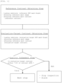
- the present invention can be performed in the following flowchart.
- FIG. 1 Described in FIG. 1 is a process example of an evaluation flowchart of the present invention using the reference mark contrast in EUV mask blank manufacturing.
- a defect inspection apparatus that can obtain the reference mark image may be used.
- a program is constructed so that a sequential process of obtaining the reference mark image, obtaining the contrast, and judging the quality (comparing the contrasts) is automatically performed.
- the reference contrast obtaining step including loading the substrate, obtaining the reference mark image, and obtaining the reference mark contrast is performed in advance on the reference EUV mask blank. That is, the reference EUV mask blank having the produced reference mark with difference depths is loaded in the apparatus, the reference mark image is obtained, and the reference contrast ⁇ REF is calculated. From the reference contrast ⁇ REF, a target depth contrast ⁇ STD is set, and a threshold in which products within ⁇ STD ⁇ 10% are judged as normal products is finally set in the evaluation apparatus.
- the evaluation-target EUV mask blank is inspected.
- the reference mark image is obtained from the evaluation-target EUV mask blank loaded in the apparatus in the reference mark image obtaining step, and the reference mark contrast (evaluation-target contrast) is automatically measured from the obtained image.
- the contrast of the inspected product evaluation-target contrast
- the preset reference value the contrast ⁇ STD set from the reference contrast ⁇ REF
- This inspection flowchart can quickly detect abnormality of the processing accuracy, such as depth, of the reference mark formed on the EUV mask blank, which has been difficult to judge the quality in the conventional method, and the process is smoothly improved.
- the reference mark contrast itself is used as the indicator.
- the depth of the reference mark which has deep correlation with the reference mark contrast, obtained by conversion of the reference mark contrast is used as the indicator.
- a reference EUV mask blank having formed reference marks with varied depth conditions is prepared in advance. Then, these reference marks are imaged, and from this reference mark image, a reference mark contrast with each depth condition is obtained (reference contrast).
- the depth of the reference mark can be measured by an AFM, etc.
- the reference mark image and the reference contrast may be obtained in the same manner as in the first embodiment.
- an evaluation-target EUV mask blank other than the reference EUV mask blank is prepared, a reference mark of the evaluation-target EUV mask blank is imaged with an optical system same as in the reference contrast obtaining step to obtain a reference mark image, and the reference mark contrast is obtained from the obtained reference mark image (evaluation-target contrast).
- the reference mark image and the evaluation-target contrast may be obtained in the same manner as in the first embodiment.
- the depth of the reference mark on the evaluation-target EUV mask blank is evaluated from the evaluation-target contrast.
- the depth-processing accuracy of the reference mark formed on the EUV mask blank can be easily evaluated without destruction, and quality of the reference mark can be judged.
- the second embodiment as above can exhibit the aforementioned effects similarly to the first embodiment.
- a predetermined percent of the target depth (this predetermined value is not limited, but specifically within ⁇ 10%) may be set as a normal value (good product).
- a lower detection limit depth of the apparatus is evaluated and determined by evaluating the reference marks having different depths on the aforementioned reference EUV mask blank, and a case of the lower detection limit depth or higher (or a case of depth deeper than the lower detection limit depth) may also be set as a normal value (good product).
- molybdenum (Mo) film and silicon (Si) films were alternately stacked by a sputtering method using a molybdenum target and a silicon target as targets, and argon as a sputtering gas to form a Mo/Si multilayer reflective film to achieve reflectance of EUV light.
- a ruthenium (Ru) film was formed as a protective film for protecting the multilayer reflective film to produce a reference EUV mask blank.
- reference marks #1 to #6 having difference depths were formed by varying processing conditions with FIB.
- Table 1 shows the measured values of the depths of the reference marks #1 to #6.
- the reference marks with 30 nm to 80 nm in depth as the measured values were formed.
- a reference mark contrast (contrasts ⁇ A to ⁇ H), which was a difference in light intensity from the background level and determined from the aforementioned formula, was calculated on sides A to H of one reference mark having design illustrated in FIG. 2 .
- An average value of these ⁇ A to ⁇ H was calculated here as a reference contrast ⁇ REF.
- Table 2 shows the results of ⁇ A to ⁇ H and ⁇ REF on the reference marks #1 to #6.
- FIG. 3 shows a graph in which the measured depth values of the reference marks #1 to #6 and the reference contrast ⁇ REF were plotted.
- Reference mark #1 #2 #3 #4 #5 #6 ⁇ A 1.06 1.14 1.15 1.21 1.28 1.37 ⁇ B 1.05 1.13 1.13 1.21 1.25 1.33 ⁇ C 1.05 1.13 1.19 1.27 1.33 1.45 ⁇ D 1.05 1.13 1.21 1.27 1.36 1.44 ⁇ E 1.05 1.14 1.16 1.22 1.29 1.37 ⁇ F 1.05 1.12 1.13 1.21 1.25 1.32 ⁇ G 1.10 1.13 1.19 1.25 1.32 1.44 ⁇ H 1.10 1.14 1.21 1.26 1.37 1.45 ⁇ REF 1.06 1.13 1.17 1.24 1.31 1.40
- Table 3 shows the ⁇ AVE of MARK 1 to 4. [Table 3] LOT (a) (b) (c) MARK1 1.21 1.18 1.06 MARK2 1.19 1.18 1.22 MARK3 1.22 1.19 1.21 MARK4 1.22 1.20 1.18
- MARK 1 of LOT (c) was judged as abnormality, and only LOT (a) and LOT (b) were judged to be treated as good products.
- the target depth of the reference mark in Examples 1 and 2 was 50 nm (range of depth-processing accuracy of good products: 45 to 55 nm).
Landscapes
- Physics & Mathematics (AREA)
- General Physics & Mathematics (AREA)
- Engineering & Computer Science (AREA)
- Quality & Reliability (AREA)
- Computer Vision & Pattern Recognition (AREA)
- Theoretical Computer Science (AREA)
- Multimedia (AREA)
- Plasma & Fusion (AREA)
- Preparing Plates And Mask In Photomechanical Process (AREA)
- Investigating Materials By The Use Of Optical Means Adapted For Particular Applications (AREA)
- Image Analysis (AREA)
- Electron Beam Exposure (AREA)
Applications Claiming Priority (1)
| Application Number | Priority Date | Filing Date | Title |
|---|---|---|---|
| JP2023064091A JP7824908B2 (ja) | 2023-04-11 | 2023-04-11 | Euvマスクブランクに形成された基準マークの評価方法 |
Publications (2)
| Publication Number | Publication Date |
|---|---|
| EP4446809A2 true EP4446809A2 (de) | 2024-10-16 |
| EP4446809A3 EP4446809A3 (de) | 2024-10-30 |
Family
ID=90571917
Family Applications (1)
| Application Number | Title | Priority Date | Filing Date |
|---|---|---|---|
| EP24167570.1A Pending EP4446809A3 (de) | 2023-04-11 | 2024-03-28 | Verfahren zur bewertung einer auf einem euv-maskenrohling geformten referenzmarkierung |
Country Status (6)
| Country | Link |
|---|---|
| US (1) | US20240345474A1 (de) |
| EP (1) | EP4446809A3 (de) |
| JP (1) | JP7824908B2 (de) |
| KR (1) | KR20240151645A (de) |
| CN (1) | CN118795721A (de) |
| TW (1) | TW202516272A (de) |
Citations (3)
| Publication number | Priority date | Publication date | Assignee | Title |
|---|---|---|---|---|
| JP2003114200A (ja) | 2001-10-05 | 2003-04-18 | National Institute Of Advanced Industrial & Technology | 多層膜マスク欠陥検査方法及び装置 |
| WO2014129527A1 (ja) | 2013-02-22 | 2014-08-28 | Hoya株式会社 | 反射型マスクブランクの製造方法、及び反射型マスクの製造方法 |
| JP2017227936A (ja) | 2012-02-10 | 2017-12-28 | Hoya株式会社 | 多層反射膜付き基板、反射型マスクブランク及び反射型マスク、マスクブランク及びマスク、多層反射膜付き基板の製造方法、反射型マスクブランクの製造方法、並びにマスクブランクの製造方法 |
Family Cites Families (8)
| Publication number | Priority date | Publication date | Assignee | Title |
|---|---|---|---|---|
| TWI431663B (zh) * | 2004-09-30 | 2014-03-21 | 尼康股份有限公司 | Measurement method and exposure method, and component manufacturing method |
| JP5768452B2 (ja) * | 2011-04-11 | 2015-08-26 | 信越化学工業株式会社 | チアニアドープ石英ガラスの製造方法 |
| US9721754B2 (en) * | 2011-04-26 | 2017-08-01 | Carl Zeiss Smt Gmbh | Method and apparatus for processing a substrate with a focused particle beam |
| KR101993322B1 (ko) * | 2011-09-28 | 2019-06-26 | 호야 가부시키가이샤 | 마스크블랭크용 유리기판, 다층 반사막 부착 기판, 마스크블랭크 및 마스크, 그리고 그것들의 제조방법 |
| DE102014213198B4 (de) * | 2014-07-08 | 2020-08-06 | Carl Zeiss Ag | Verfahren zur Lokalisierung von Defekten auf Substraten |
| US9786057B2 (en) * | 2014-09-19 | 2017-10-10 | Lasertec Coporation | Inspection apparatus, coordinate detection apparatus, coordinate detection method, and wavefront aberration correction method |
| DE102015213045B4 (de) * | 2015-07-13 | 2018-05-24 | Carl Zeiss Smt Gmbh | Verfahren und Vorrichtung zur Positionsbestimmung von Strukturelementen einer photolithographischen Maske |
| JP7017475B2 (ja) * | 2018-06-19 | 2022-02-08 | 信越化学工業株式会社 | フォトマスクブランク関連基板の表面状態の評価方法 |
-
2023
- 2023-04-11 JP JP2023064091A patent/JP7824908B2/ja active Active
-
2024
- 2024-03-28 EP EP24167570.1A patent/EP4446809A3/de active Pending
- 2024-03-29 US US18/621,633 patent/US20240345474A1/en active Pending
- 2024-04-03 KR KR1020240045019A patent/KR20240151645A/ko active Pending
- 2024-04-08 CN CN202410415427.1A patent/CN118795721A/zh active Pending
- 2024-04-10 TW TW113113254A patent/TW202516272A/zh unknown
Patent Citations (3)
| Publication number | Priority date | Publication date | Assignee | Title |
|---|---|---|---|---|
| JP2003114200A (ja) | 2001-10-05 | 2003-04-18 | National Institute Of Advanced Industrial & Technology | 多層膜マスク欠陥検査方法及び装置 |
| JP2017227936A (ja) | 2012-02-10 | 2017-12-28 | Hoya株式会社 | 多層反射膜付き基板、反射型マスクブランク及び反射型マスク、マスクブランク及びマスク、多層反射膜付き基板の製造方法、反射型マスクブランクの製造方法、並びにマスクブランクの製造方法 |
| WO2014129527A1 (ja) | 2013-02-22 | 2014-08-28 | Hoya株式会社 | 反射型マスクブランクの製造方法、及び反射型マスクの製造方法 |
Also Published As
| Publication number | Publication date |
|---|---|
| EP4446809A3 (de) | 2024-10-30 |
| JP2024150994A (ja) | 2024-10-24 |
| TW202516272A (zh) | 2025-04-16 |
| CN118795721A (zh) | 2024-10-18 |
| US20240345474A1 (en) | 2024-10-17 |
| JP7824908B2 (ja) | 2026-03-05 |
| KR20240151645A (ko) | 2024-10-18 |
Similar Documents
| Publication | Publication Date | Title |
|---|---|---|
| US11852964B2 (en) | Method for manufacturing reflective mask blank, reflective mask blank, method for manufacturing reflective mask, reflective mask, and method for manufacturing semiconductor device | |
| JP6342436B2 (ja) | Euvフォトマスクの欠陥を解析かつ除去する方法及び装置 | |
| JP5502450B2 (ja) | 反射型露光用マスク、反射型露光用マスクの検査方法、及び反射型露光用マスクの洗浄方法 | |
| JP4853685B2 (ja) | フォトマスクブランク又はその製造中間体の検査方法及び良否判定方法 | |
| KR102546566B1 (ko) | 반사형 마스크 블랭크의 제조 방법, 반사형 마스크 블랭크 및 반사형 마스크의 제조 방법 | |
| KR20170051506A (ko) | 극자외선 파장 범위용 마스크를 제조하는 방법, 마스크 및 장치 | |
| KR102127904B1 (ko) | 반사형 마스크 블랭크 및 그 제조 방법, 그리고 반사형 마스크 | |
| JP2011187746A (ja) | 反射型マスクブランクス、反射型マスク、およびその製造方法 | |
| JP2013149875A (ja) | 位相欠陥の影響を低減するeuv露光用反射型マスクの製造方法 | |
| CN110618582B (zh) | 光掩膜坯料关联基板的评价方法 | |
| KR20060132680A (ko) | 광학 검사 장치, 광학 검사 방법, 피사체 제조 방법 및마스크 | |
| US20240345474A1 (en) | Method for evaluating reference mark formed on euv mask blank | |
| JP6394422B2 (ja) | 欠陥検査方法及び検査光の照射方法 | |
| Okoroanyanwu et al. | Towards the optical inspection sensitivity optimization of EUV masks and EUVL-exposed wafers | |
| JP2001093951A (ja) | 欠陥検査用半導体基板、半導体基板の検査方法および半導体基板検査用モニター装置 | |
| US20250390014A1 (en) | Reflective mask blank and method for manufacturing the same, and method for inspecting reflective mask blank-related substrate | |
| JP2014090131A (ja) | 反射型マスクの製造方法 | |
| JP7645092B2 (ja) | 反射型マスクブランク、反射型マスクおよび反射型マスクの製造方法 | |
| CN112639612A (zh) | 决定要引入光刻掩模的基板的一个或多个像素的效应的方法和设备 | |
| JP2007273652A (ja) | 極端紫外線露光用マスクブランク及び極端紫外線露光用マスク並びにパターン転写方法 | |
| TW202419960A (zh) | 附薄膜基板之製造方法、附薄膜基板、附多層反射膜基板之製造方法、附多層反射膜基板、反射型遮罩基底、反射型遮罩之製造方法、及半導體裝置之製造方法 | |
| JP2016031972A (ja) | 反射型マスクブランク及びその製造方法並びに反射型マスク |
Legal Events
| Date | Code | Title | Description |
|---|---|---|---|
| PUAI | Public reference made under article 153(3) epc to a published international application that has entered the european phase |
Free format text: ORIGINAL CODE: 0009012 |
|
| STAA | Information on the status of an ep patent application or granted ep patent |
Free format text: STATUS: THE APPLICATION HAS BEEN PUBLISHED |
|
| REG | Reference to a national code |
Ref country code: DE Ref legal event code: R079 Free format text: PREVIOUS MAIN CLASS: G03F0001220000 Ipc: G03F0001240000 |
|
| PUAL | Search report despatched |
Free format text: ORIGINAL CODE: 0009013 |
|
| AK | Designated contracting states |
Kind code of ref document: A2 Designated state(s): AL AT BE BG CH CY CZ DE DK EE ES FI FR GB GR HR HU IE IS IT LI LT LU LV MC ME MK MT NL NO PL PT RO RS SE SI SK SM TR |
|
| AK | Designated contracting states |
Kind code of ref document: A3 Designated state(s): AL AT BE BG CH CY CZ DE DK EE ES FI FR GB GR HR HU IE IS IT LI LT LU LV MC ME MK MT NL NO PL PT RO RS SE SI SK SM TR |
|
| RIC1 | Information provided on ipc code assigned before grant |
Ipc: G03F 1/84 20120101ALI20240924BHEP Ipc: G03F 1/38 20120101ALI20240924BHEP Ipc: G03F 1/24 20120101AFI20240924BHEP |
|
| STAA | Information on the status of an ep patent application or granted ep patent |
Free format text: STATUS: REQUEST FOR EXAMINATION WAS MADE |
|
| 17P | Request for examination filed |
Effective date: 20250218 |