EP4443235A2 - Reflektierender maskenrohling und herstellungsverfahren für reflektierende maske - Google Patents
Reflektierender maskenrohling und herstellungsverfahren für reflektierende maske Download PDFInfo
- Publication number
- EP4443235A2 EP4443235A2 EP24164620.7A EP24164620A EP4443235A2 EP 4443235 A2 EP4443235 A2 EP 4443235A2 EP 24164620 A EP24164620 A EP 24164620A EP 4443235 A2 EP4443235 A2 EP 4443235A2
- Authority
- EP
- European Patent Office
- Prior art keywords
- film
- layer
- absorber
- gas
- oxygen
- Prior art date
- Legal status (The legal status is an assumption and is not a legal conclusion. Google has not performed a legal analysis and makes no representation as to the accuracy of the status listed.)
- Pending
Links
- 238000004519 manufacturing process Methods 0.000 title claims description 13
- 239000006096 absorbing agent Substances 0.000 claims abstract description 131
- 239000000758 substrate Substances 0.000 claims abstract description 88
- IJGRMHOSHXDMSA-UHFFFAOYSA-N Atomic nitrogen Chemical compound N#N IJGRMHOSHXDMSA-UHFFFAOYSA-N 0.000 claims abstract description 75
- QVGXLLKOCUKJST-UHFFFAOYSA-N atomic oxygen Chemical compound [O] QVGXLLKOCUKJST-UHFFFAOYSA-N 0.000 claims abstract description 72
- 239000001301 oxygen Substances 0.000 claims abstract description 72
- 229910052760 oxygen Inorganic materials 0.000 claims abstract description 72
- 239000000463 material Substances 0.000 claims abstract description 65
- 239000011651 chromium Substances 0.000 claims abstract description 54
- 239000000203 mixture Substances 0.000 claims abstract description 49
- 229910052715 tantalum Inorganic materials 0.000 claims abstract description 47
- GUVRBAGPIYLISA-UHFFFAOYSA-N tantalum atom Chemical compound [Ta] GUVRBAGPIYLISA-UHFFFAOYSA-N 0.000 claims abstract description 47
- 229910052757 nitrogen Inorganic materials 0.000 claims abstract description 36
- KJTLSVCANCCWHF-UHFFFAOYSA-N Ruthenium Chemical compound [Ru] KJTLSVCANCCWHF-UHFFFAOYSA-N 0.000 claims abstract description 33
- 229910052707 ruthenium Inorganic materials 0.000 claims abstract description 33
- 229910052804 chromium Inorganic materials 0.000 claims abstract description 27
- VYZAMTAEIAYCRO-UHFFFAOYSA-N Chromium Chemical compound [Cr] VYZAMTAEIAYCRO-UHFFFAOYSA-N 0.000 claims abstract description 26
- 239000007789 gas Substances 0.000 claims description 124
- 238000001312 dry etching Methods 0.000 claims description 66
- 238000005530 etching Methods 0.000 claims description 40
- 238000011282 treatment Methods 0.000 claims description 35
- ZAMOUSCENKQFHK-UHFFFAOYSA-N Chlorine atom Chemical compound [Cl] ZAMOUSCENKQFHK-UHFFFAOYSA-N 0.000 claims description 34
- 239000000460 chlorine Substances 0.000 claims description 34
- 229910052801 chlorine Inorganic materials 0.000 claims description 34
- 239000010955 niobium Substances 0.000 claims description 31
- 238000000034 method Methods 0.000 claims description 27
- XEMZLVDIUVCKGL-UHFFFAOYSA-N hydrogen peroxide;sulfuric acid Chemical compound OO.OS(O)(=O)=O XEMZLVDIUVCKGL-UHFFFAOYSA-N 0.000 claims description 16
- 229910052758 niobium Inorganic materials 0.000 claims description 14
- GUCVJGMIXFAOAE-UHFFFAOYSA-N niobium atom Chemical compound [Nb] GUCVJGMIXFAOAE-UHFFFAOYSA-N 0.000 claims description 14
- 239000000126 substance Substances 0.000 claims description 9
- YCKRFDGAMUMZLT-UHFFFAOYSA-N Fluorine atom Chemical compound [F] YCKRFDGAMUMZLT-UHFFFAOYSA-N 0.000 claims description 7
- 229910052731 fluorine Inorganic materials 0.000 claims description 7
- 239000011737 fluorine Substances 0.000 claims description 7
- 239000000956 alloy Substances 0.000 claims description 6
- 229910045601 alloy Inorganic materials 0.000 claims description 6
- 238000001900 extreme ultraviolet lithography Methods 0.000 claims description 5
- 239000010410 layer Substances 0.000 description 183
- 238000004544 sputter deposition Methods 0.000 description 29
- 238000011156 evaluation Methods 0.000 description 20
- 229910003071 TaON Inorganic materials 0.000 description 17
- 230000000052 comparative effect Effects 0.000 description 15
- MWUXSHHQAYIFBG-UHFFFAOYSA-N nitrogen oxide Inorganic materials O=[N] MWUXSHHQAYIFBG-UHFFFAOYSA-N 0.000 description 14
- OKTJSMMVPCPJKN-UHFFFAOYSA-N Carbon Chemical compound [C] OKTJSMMVPCPJKN-UHFFFAOYSA-N 0.000 description 12
- 229910052799 carbon Inorganic materials 0.000 description 12
- ZOXJGFHDIHLPTG-UHFFFAOYSA-N Boron Chemical compound [B] ZOXJGFHDIHLPTG-UHFFFAOYSA-N 0.000 description 11
- GQPLMRYTRLFLPF-UHFFFAOYSA-N Nitrous Oxide Chemical compound [O-][N+]#N GQPLMRYTRLFLPF-UHFFFAOYSA-N 0.000 description 11
- 229910052796 boron Inorganic materials 0.000 description 11
- 230000007423 decrease Effects 0.000 description 11
- 239000000654 additive Substances 0.000 description 10
- 230000000996 additive effect Effects 0.000 description 10
- 238000001755 magnetron sputter deposition Methods 0.000 description 10
- XUIMIQQOPSSXEZ-UHFFFAOYSA-N Silicon Chemical compound [Si] XUIMIQQOPSSXEZ-UHFFFAOYSA-N 0.000 description 9
- 238000004140 cleaning Methods 0.000 description 9
- 229910052710 silicon Inorganic materials 0.000 description 9
- 239000010703 silicon Substances 0.000 description 9
- XKRFYHLGVUSROY-UHFFFAOYSA-N Argon Chemical compound [Ar] XKRFYHLGVUSROY-UHFFFAOYSA-N 0.000 description 8
- CURLTUGMZLYLDI-UHFFFAOYSA-N Carbon dioxide Chemical compound O=C=O CURLTUGMZLYLDI-UHFFFAOYSA-N 0.000 description 8
- 229910052751 metal Inorganic materials 0.000 description 8
- 239000002184 metal Substances 0.000 description 8
- 239000001257 hydrogen Substances 0.000 description 7
- 229910052739 hydrogen Inorganic materials 0.000 description 7
- 229910052752 metalloid Inorganic materials 0.000 description 7
- 150000002738 metalloids Chemical class 0.000 description 7
- 230000003647 oxidation Effects 0.000 description 7
- 238000007254 oxidation reaction Methods 0.000 description 7
- ZOKXTWBITQBERF-UHFFFAOYSA-N Molybdenum Chemical compound [Mo] ZOKXTWBITQBERF-UHFFFAOYSA-N 0.000 description 6
- 238000009616 inductively coupled plasma Methods 0.000 description 6
- 238000007689 inspection Methods 0.000 description 6
- 229910052750 molybdenum Inorganic materials 0.000 description 6
- 239000011733 molybdenum Substances 0.000 description 6
- 238000001020 plasma etching Methods 0.000 description 6
- MGWGWNFMUOTEHG-UHFFFAOYSA-N 4-(3,5-dimethylphenyl)-1,3-thiazol-2-amine Chemical compound CC1=CC(C)=CC(C=2N=C(N)SC=2)=C1 MGWGWNFMUOTEHG-UHFFFAOYSA-N 0.000 description 4
- UGFAIRIUMAVXCW-UHFFFAOYSA-N Carbon monoxide Chemical compound [O+]#[C-] UGFAIRIUMAVXCW-UHFFFAOYSA-N 0.000 description 4
- UFHFLCQGNIYNRP-UHFFFAOYSA-N Hydrogen Chemical compound [H][H] UFHFLCQGNIYNRP-UHFFFAOYSA-N 0.000 description 4
- QAOWNCQODCNURD-UHFFFAOYSA-N Sulfuric acid Chemical compound OS(O)(=O)=O QAOWNCQODCNURD-UHFFFAOYSA-N 0.000 description 4
- 229910052786 argon Inorganic materials 0.000 description 4
- 239000001569 carbon dioxide Substances 0.000 description 4
- 229910002092 carbon dioxide Inorganic materials 0.000 description 4
- 229910002091 carbon monoxide Inorganic materials 0.000 description 4
- 150000001875 compounds Chemical class 0.000 description 4
- 230000003247 decreasing effect Effects 0.000 description 4
- 239000001307 helium Substances 0.000 description 4
- 229910052734 helium Inorganic materials 0.000 description 4
- SWQJXJOGLNCZEY-UHFFFAOYSA-N helium atom Chemical compound [He] SWQJXJOGLNCZEY-UHFFFAOYSA-N 0.000 description 4
- 229910052743 krypton Inorganic materials 0.000 description 4
- DNNSSWSSYDEUBZ-UHFFFAOYSA-N krypton atom Chemical compound [Kr] DNNSSWSSYDEUBZ-UHFFFAOYSA-N 0.000 description 4
- JCXJVPUVTGWSNB-UHFFFAOYSA-N nitrogen dioxide Inorganic materials O=[N]=O JCXJVPUVTGWSNB-UHFFFAOYSA-N 0.000 description 4
- 239000001272 nitrous oxide Substances 0.000 description 4
- 230000003287 optical effect Effects 0.000 description 4
- 239000004065 semiconductor Substances 0.000 description 4
- 239000010936 titanium Substances 0.000 description 4
- 229910052724 xenon Inorganic materials 0.000 description 4
- FHNFHKCVQCLJFQ-UHFFFAOYSA-N xenon atom Chemical compound [Xe] FHNFHKCVQCLJFQ-UHFFFAOYSA-N 0.000 description 4
- 229910020442 SiO2—TiO2 Inorganic materials 0.000 description 3
- 229910002090 carbon oxide Inorganic materials 0.000 description 3
- 239000011521 glass Substances 0.000 description 3
- 150000002431 hydrogen Chemical class 0.000 description 3
- VNWKTOKETHGBQD-UHFFFAOYSA-N methane Chemical compound C VNWKTOKETHGBQD-UHFFFAOYSA-N 0.000 description 3
- QJGQUHMNIGDVPM-UHFFFAOYSA-N nitrogen group Chemical group [N] QJGQUHMNIGDVPM-UHFFFAOYSA-N 0.000 description 3
- 238000000059 patterning Methods 0.000 description 3
- 238000005546 reactive sputtering Methods 0.000 description 3
- VSZWPYCFIRKVQL-UHFFFAOYSA-N selanylidenegallium;selenium Chemical compound [Se].[Se]=[Ga].[Se]=[Ga] VSZWPYCFIRKVQL-UHFFFAOYSA-N 0.000 description 3
- 230000003746 surface roughness Effects 0.000 description 3
- ITWBWJFEJCHKSN-UHFFFAOYSA-N 1,4,7-triazonane Chemical compound C1CNCCNCCN1 ITWBWJFEJCHKSN-UHFFFAOYSA-N 0.000 description 2
- KZBUYRJDOAKODT-UHFFFAOYSA-N Chlorine Chemical compound ClCl KZBUYRJDOAKODT-UHFFFAOYSA-N 0.000 description 2
- MHAJPDPJQMAIIY-UHFFFAOYSA-N Hydrogen peroxide Chemical compound OO MHAJPDPJQMAIIY-UHFFFAOYSA-N 0.000 description 2
- RTAQQCXQSZGOHL-UHFFFAOYSA-N Titanium Chemical compound [Ti] RTAQQCXQSZGOHL-UHFFFAOYSA-N 0.000 description 2
- 239000007864 aqueous solution Substances 0.000 description 2
- 238000010586 diagram Methods 0.000 description 2
- 238000010894 electron beam technology Methods 0.000 description 2
- 239000002356 single layer Substances 0.000 description 2
- 229910052719 titanium Inorganic materials 0.000 description 2
- 239000004215 Carbon black (E152) Substances 0.000 description 1
- VYPSYNLAJGMNEJ-UHFFFAOYSA-N Silicium dioxide Chemical compound O=[Si]=O VYPSYNLAJGMNEJ-UHFFFAOYSA-N 0.000 description 1
- 229910052782 aluminium Inorganic materials 0.000 description 1
- XAGFODPZIPBFFR-UHFFFAOYSA-N aluminium Chemical compound [Al] XAGFODPZIPBFFR-UHFFFAOYSA-N 0.000 description 1
- ISQINHMJILFLAQ-UHFFFAOYSA-N argon hydrofluoride Chemical compound F.[Ar] ISQINHMJILFLAQ-UHFFFAOYSA-N 0.000 description 1
- 230000008033 biological extinction Effects 0.000 description 1
- LGLOITKZTDVGOE-UHFFFAOYSA-N boranylidynemolybdenum Chemical compound [Mo]#B LGLOITKZTDVGOE-UHFFFAOYSA-N 0.000 description 1
- 150000001845 chromium compounds Chemical class 0.000 description 1
- 238000011109 contamination Methods 0.000 description 1
- 230000007547 defect Effects 0.000 description 1
- 230000003111 delayed effect Effects 0.000 description 1
- 238000001514 detection method Methods 0.000 description 1
- 230000006866 deterioration Effects 0.000 description 1
- 230000000694 effects Effects 0.000 description 1
- 238000000295 emission spectrum Methods 0.000 description 1
- 229910052732 germanium Inorganic materials 0.000 description 1
- GNPVGFCGXDBREM-UHFFFAOYSA-N germanium atom Chemical compound [Ge] GNPVGFCGXDBREM-UHFFFAOYSA-N 0.000 description 1
- 238000010438 heat treatment Methods 0.000 description 1
- 229930195733 hydrocarbon Natural products 0.000 description 1
- 150000002430 hydrocarbons Chemical class 0.000 description 1
- 238000001659 ion-beam spectroscopy Methods 0.000 description 1
- 238000010884 ion-beam technique Methods 0.000 description 1
- 150000002500 ions Chemical class 0.000 description 1
- 230000001678 irradiating effect Effects 0.000 description 1
- 238000010030 laminating Methods 0.000 description 1
- 239000007788 liquid Substances 0.000 description 1
- 229910052754 neon Inorganic materials 0.000 description 1
- GKAOGPIIYCISHV-UHFFFAOYSA-N neon atom Chemical compound [Ne] GKAOGPIIYCISHV-UHFFFAOYSA-N 0.000 description 1
- 150000004767 nitrides Chemical class 0.000 description 1
- 238000000206 photolithography Methods 0.000 description 1
- 238000005498 polishing Methods 0.000 description 1
- 238000001552 radio frequency sputter deposition Methods 0.000 description 1
Images
Classifications
-
- G—PHYSICS
- G03—PHOTOGRAPHY; CINEMATOGRAPHY; ANALOGOUS TECHNIQUES USING WAVES OTHER THAN OPTICAL WAVES; ELECTROGRAPHY; HOLOGRAPHY
- G03F—PHOTOMECHANICAL PRODUCTION OF TEXTURED OR PATTERNED SURFACES, e.g. FOR PRINTING, FOR PROCESSING OF SEMICONDUCTOR DEVICES; MATERIALS THEREFOR; ORIGINALS THEREFOR; APPARATUS SPECIALLY ADAPTED THEREFOR
- G03F1/00—Originals for photomechanical production of textured or patterned surfaces, e.g., masks, photo-masks, reticles; Mask blanks or pellicles therefor; Containers specially adapted therefor; Preparation thereof
- G03F1/22—Masks or mask blanks for imaging by radiation of 100nm or shorter wavelength, e.g. X-ray masks, extreme ultraviolet [EUV] masks; Preparation thereof
- G03F1/24—Reflection masks; Preparation thereof
-
- G—PHYSICS
- G03—PHOTOGRAPHY; CINEMATOGRAPHY; ANALOGOUS TECHNIQUES USING WAVES OTHER THAN OPTICAL WAVES; ELECTROGRAPHY; HOLOGRAPHY
- G03F—PHOTOMECHANICAL PRODUCTION OF TEXTURED OR PATTERNED SURFACES, e.g. FOR PRINTING, FOR PROCESSING OF SEMICONDUCTOR DEVICES; MATERIALS THEREFOR; ORIGINALS THEREFOR; APPARATUS SPECIALLY ADAPTED THEREFOR
- G03F1/00—Originals for photomechanical production of textured or patterned surfaces, e.g., masks, photo-masks, reticles; Mask blanks or pellicles therefor; Containers specially adapted therefor; Preparation thereof
- G03F1/38—Masks having auxiliary features, e.g. special coatings or marks for alignment or testing; Preparation thereof
- G03F1/48—Protective coatings
-
- G—PHYSICS
- G03—PHOTOGRAPHY; CINEMATOGRAPHY; ANALOGOUS TECHNIQUES USING WAVES OTHER THAN OPTICAL WAVES; ELECTROGRAPHY; HOLOGRAPHY
- G03F—PHOTOMECHANICAL PRODUCTION OF TEXTURED OR PATTERNED SURFACES, e.g. FOR PRINTING, FOR PROCESSING OF SEMICONDUCTOR DEVICES; MATERIALS THEREFOR; ORIGINALS THEREFOR; APPARATUS SPECIALLY ADAPTED THEREFOR
- G03F1/00—Originals for photomechanical production of textured or patterned surfaces, e.g., masks, photo-masks, reticles; Mask blanks or pellicles therefor; Containers specially adapted therefor; Preparation thereof
- G03F1/54—Absorbers, e.g. of opaque materials
- G03F1/58—Absorbers, e.g. of opaque materials having two or more different absorber layers, e.g. stacked multilayer absorbers
-
- G—PHYSICS
- G03—PHOTOGRAPHY; CINEMATOGRAPHY; ANALOGOUS TECHNIQUES USING WAVES OTHER THAN OPTICAL WAVES; ELECTROGRAPHY; HOLOGRAPHY
- G03F—PHOTOMECHANICAL PRODUCTION OF TEXTURED OR PATTERNED SURFACES, e.g. FOR PRINTING, FOR PROCESSING OF SEMICONDUCTOR DEVICES; MATERIALS THEREFOR; ORIGINALS THEREFOR; APPARATUS SPECIALLY ADAPTED THEREFOR
- G03F1/00—Originals for photomechanical production of textured or patterned surfaces, e.g., masks, photo-masks, reticles; Mask blanks or pellicles therefor; Containers specially adapted therefor; Preparation thereof
- G03F1/68—Preparation processes not covered by groups G03F1/20 - G03F1/50
- G03F1/80—Etching
Definitions
- the present invention relates to a reflective mask blank which is a material for a reflective mask used in manufacturing semiconductor devices such as LSIs, and a manufacturing method of the reflective mask from the reflective mask blank.
- a photolithography technique in which a circuit pattern formed on a transfer mask is transferred onto a semiconductor substrate (a semiconductor wafer) through a reduction projection optical system with irradiating exposure light to the transfer mask is repeatedly used.
- a mainstream wavelength of the exposure light is 193 nm by argon fluoride (ArF) excimer laser light.
- a pattern with dimensions smaller than exposure wavelength has finally been formed by adopting a process called multi-patterning in which exposure processes and processing processes are combined multiple times.
- EUV extreme ultraviolet
- the EUV light is light having a wavelength of about 0.2 to 100 nm, in particular, light having a wavelength of around 13.5 nm.
- the EUV light has a very low transparency to a substance and cannot be utilized for a conventional transmissive projection optical system or a mask, thus, a reflection type optical elemental device is applied. Therefore, a reflective mask is also used as a mask for the pattern transfer.
- a multilayer reflection film that reflects EUV light is formed on a substrate, and further an absorber film formed in a pattern that absorbs EUV light is formed on the multilayer reflection film.
- a material (including also a state in which a resist layer is formed) before patterning the absorber film is called a reflective mask blank, and is used as a material for the reflective mask.
- the reflective mask blank generally has a basic structure including a low thermal expansion substrate, a multilayer reflection film that is formed on one surface of two main surface of the substrate and reflects EUV light, and an absorber film that is formed thereon and absorbs EUV light.
- the multilayer reflection film As the multilayer reflection film, a multilayer reflection film which is ensured a necessary reflectance for EUV light by alternately laminating molybdenum (Mo) layers and silicon (Si) layers is commonly used. On the other hand, tantalum (Ta) which has a relatively large extinction coefficient with respect to EUV light is used for the absorber film (Patent Document 1: JP-A 2002-246299 ).
- a ruthenium (Ru) film is formed on the multilayer reflection film, as disclosed in JP-A 2002-122981 (Patent Document 2).
- a hard mask film containing chromium (Cr) is formed on the absorber film in some cases.
- a conductive film is formed on the other main surface of the substrate.
- a metal nitride film is proposed for electrostatically chucking, and a film containing chromium (Cr) or tantalum (Ta) is exemplified.
- the protection film is required to have function for protecting the multilayer reflection film.
- function for protecting a multilayer reflection film so as not to expose the multilayer reflection film to etching gases and cleaning liquids in processing a pattern of an absorber film and function for suppressing decrease of reflectance due to repeated exposure in exposing using a reflective mask are exemplified.
- the protection film is exposed to etching, and is damaged.
- the absorber film is composed of a material containing tantalum (Ta)
- a gas containing chlorine and being free of oxygen is preferably used as an etching gas. Therefore, the protection film is required to have resistance to dry etching using a gas containing chlorine and being free of oxygen.
- a hard mask pattern which is obtained by forming a pattern of a hard mask film composed of a material containing chromium (Cr) is used as an etching mask in forming a pattern to the absorber film
- the pattern of the hard mask film is removed by dry etching using a gas containing chlorine and oxygen.
- the protection film is also exposed to the dry etching using a gas containing chlorine and oxygen at that time. Therefore, resistance to dry etching using a gas containing chlorine and oxygen is also required for the protection film.
- the protection film is also required to have resistance to a sulfuric acid-hydrogen peroxide mixture (SPM).
- the protection film is damaged in etching in manufacturing the reflective mask, and changes in film quality and thickness are caused, problems such as loss of the function for protecting the multilayer reflection film are occurred in the protection film. Therefore, with respect to the protection film containing ruthenium (Ru), a protection film added with an additive element such as niobium (Nb) has been proposed to enhance the function for protecting the multilayer reflection film by improving the resistance to dry etching.
- Ru ruthenium
- Nb niobium
- the protection film will be thinned when the protection film is exposed to a gas containing chlorine and being free of oxygen in dry etching to the absorber film composed of a material containing tantalum (Ta). Further, the protection film will be also thinned when the protection film is exposed to a gas containing chlorine and oxygen in removing the pattern of the hard mask film. Furthermore, the protection film will be also thinned in cleaning using a sulfuric acid-hydrogen peroxide mixture (SPM).
- SPM sulfuric acid-hydrogen peroxide mixture
- the present invention has been made to solve the above problems, and an object of the present invention is to provide, as a reflective mask blank in which an absorber film composed of a material containing tantalum (Ta) is formed on a protection film composed of a material containing ruthenium (Ru), a reflective mask blank including an absorber film that can reduce damage of the protection film caused by over-etching of the absorber film composed of a material containing tantalum (Ta) using a gas containing chlorine and being free of oxygen, and can control decrease of thickness of the protection film caused by dry etching using a gas containing chlorine and oxygen, or cleaning using a sulfuric acid-hydrogen peroxide mixture (SPM).
- Another object of the present invention is to provide a method for manufacturing a reflective mask using the reflective mask blank.
- the inventors have made earnestly studies to solve the above problems. As a result, the inventors found, with respect to a reflective mask blank in which an absorber film composed of a material containing tantalum (Ta) is formed on a protection film composed of a material containing ruthenium (Ru), the absorber film having a structure including, from a substrate side, a first layer having a composition containing tantalum (Ta) and being free of nitrogen (N), and a second layer having a composition containing tantalum (Ta) and nitrogen (N).
- a reflective mask blank in which an absorber film composed of a material containing tantalum (Ta) is formed on a protection film composed of a material ruthenium (Ru), the absorber film having a structure including, from a substrate side, a first layer having a composition containing tantalum (Ta) and being free of nitrogen (N), and a second layer having a composition containing tantalum (Ta) and nitrogen (N).
- the reflective mask blank having the structure can reduce damage of the protection film caused by over-etching of the absorber film composed of a material containing tantalum (Ta) using a gas containing chlorine and being free of oxygen, and can control decrease of thickness of the protection film caused by dry etching using a gas containing chlorine and oxygen, or cleaning using a sulfuric acid-hydrogen peroxide mixture (SPM).
- SPM sulfuric acid-hydrogen peroxide mixture
- the invention provides a reflective mask blank including a substrate, a multilayer reflection film that is formed on one main surface of the substrate and reflects exposure light, a protection film that is formed on and in contact with the multilayer reflection film, an absorber film that is formed on and in contact with the protection film and absorbs the exposure light, and a hard mask film that is formed on and in contact with the absorber film and acts as an etching mask in dry etching of the absorber film, the reflective mask blank being a material for a reflective mask that is used in EUV lithography utilizing EUV light as the exposure light wherein,
- the composition of the first layer further contains oxygen (O).
- the composition of the first layer has an oxygen (O) content of not less than 5 at%.
- the composition of the second layer has a tantalum (Ta) content of not less than 55 at% and not more than 70 at%, and a nitrogen (N) content of not less than 30 at% and not more than 45 at%.
- Ta tantalum
- N nitrogen
- the material containing ruthenium (Ru) is simple substance of ruthenium (Ru), or an alloy consisting of ruthenium (Ru) and niobium (Nb).
- the alloy consisting of ruthenium (Ru) and niobium (Nb) has a niobium (Nb) content of not more than 30 at% on average for the whole of the protection film.
- the invention provides a method for manufacturing a reflective mask, including the steps of:
- the dry etching is performed so as to expose the protection film.
- the dry etching is performed so as to remain a part of the absorber film without exposing the protection film, and in the step (F), the dry etching is performed so as to expose the protection film.
- the method further includes (G) after the step (F), a step including a treatment of contacting the exposed absorber film with a sulfuric acid-hydrogen peroxide mixture (SPM).
- SPM sulfuric acid-hydrogen peroxide mixture
- the method further includes (G) after the step (F), a step including a treatment of contacting the exposed absorber film with a sulfuric acid-hydrogen peroxide mixture (SPM), wherein
- SPM sulfuric acid-hydrogen peroxide mixture
- the absorber film consists of, from the substrate side, a first layer, a second layer and a third layer
- the method further includes the step of: (C-1) after the step (C) and before the step (D), forming a pattern of the third layer in the absorber film by dry etching the third layer in the absorber film with using a fluorine-based gas and utilizing the pattern of the hard mask film.
- the inventive reflective mask blank can reduce damage of a protection film caused by over-etching of an absorber film composed of a material containing tantalum (Ta) using a gas containing chlorine and being free of oxygen. Further, the inventive reflective mask blank can control decrease of thickness of the protection film caused by dry etching using a gas containing chlorine and oxygen, or cleaning using a sulfuric acid-hydrogen peroxide mixture (SPM).
- SPM sulfuric acid-hydrogen peroxide mixture
- a reflective mask blank of the invention includes a substrate, a multilayer reflection film that is formed on one main surface (front-side surface) of the substrate) and reflects exposure light, a protection film that is formed on the multilayer reflection film, an absorber film that is formed on the protection film and absorbs the exposure light, and a hard mask film that is formed on the absorber film.
- the reflective mask blank of the invention is suitable for a material for a reflective mask used in EUV lithography utilizing EUV light as exposure light.
- a wavelength of EUV light used in EUV lithography utilizing EUV light as exposure light is 13 to 14 nm, normally about 13.5 nm.
- a reflective mask blank and a reflective mask utilizing EUV light as exposure light are also called an EUV mask blank and an EUV mask, respectively.
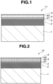
- FIG. 1 is a cross-sectional view illustrating an example of a reflective mask blank of the invention.
- This reflective mask blank 11 includes a substrate 1, and, on the substrate 1, a multilayer reflection film 2 that is formed in contact with the substrate 1, a protection film 3 that is formed in contact with the multilayer reflection film 2, an absorber film 4 that is formed in contact with the protection film 3, and a hard mask film 5 that is formed in contact with the absorber film 4.
- the absorber film 4 has a structure consisting of two layers of, from the substrate 1 side, a first layer 41 and a second layer 42.
- FIG. 2 is a cross-sectional view illustrating another example of a reflective mask blank of the invention.
- This reflective mask blank 12 includes a substrate 1, and, on the substrate 1, a multilayer reflection film 2 that is formed in contact with the substrate 1, a protection film 3 that is formed in contact with the multilayer reflection film 2, an absorber film 4 that is formed in contact with the protection film 3, and a hard mask film 5 that is formed in contact with the absorber film 4.
- the absorber film 4 has a structure consisting of three layers of, from the substrate 1 side, a first layer 41, a second layer 42 and a third layer 43.
- the substrate preferably has low thermal expansion property.
- the substrate is composed of a material having a coefficient of thermal expansion preferably within ⁇ 2 ⁇ 10 -8 /°C, more preferably within ⁇ 5 ⁇ 10 -9 /°C.
- a titania-doped quartz glass SiO 2 -TiO 2 -based glass
- a substrate having a sufficiently flatted surface is preferably used.
- the main surface of the substrate has a surface roughness, as an RMS value, of preferably not more than 0.5 nm, more preferably not more than 0.2 nm. Such a surface roughness can be obtained by polishing the substrate or other methods.
- the main surface of the substrate preferably has a 152 mm-square, and the substrate preferably has a 6.35 mm-thick.
- a substrate having the dimensions is so-called a 6025 substrate (a substrate having dimensions of the main surface of a 6 inches-square and 0.25 inches-thick).
- the multilayer reflection film is a film that reflects exposure light, in the reflective mask.
- the multilayer reflection film is preferably formed in contact with one main surface of the substrate, however, may be formed via another film such as an underlayer film on the one main surface of the substrate.
- the multilayer reflection film has a periodically laminated structure in which high refractive index layers having a comparatively high refractive index with respect to exposure light and low refractive index layers having a comparatively low refractive index with respect to the exposure light are alternately laminated.
- the high refractive index layer is preferably composed of a material containing silicon (Si).
- the high refractive index layer may contain at least one additive element selected from the group consisting of oxygen (O), nitrogen (N), carbon (C), boron (B) and hydrogen (H).
- the high refractive index layer may be configured by a multilayer including a layer containing the additive element and a layer not containing the additive element.
- the high refractive index layer has a thickness of preferably not less than 3.5 nm, more preferably not less than 4 nm, and preferably not more than 4.9 nm, more preferably not more than 4.4 nm.
- the low refractive index layer is preferably composed of a material containing molybdenum (Mo).
- the low refractive index layer may contain at least one additive element selected from the group consisting of oxygen (O), nitrogen (N), carbon (C), boron (B) and hydrogen (H).
- the low refractive index layer may be configured by a multilayer including a layer containing the additive element and a layer not containing the additive element.
- the low refractive index layer has a thickness of preferably not less than 2.1 nm, more preferably not less than 2.6 nm, and preferably not more than 3.5 nm, more preferably not more than 3 nm.
- a laminated structure constituting the periodically laminated structure may include the high refractive index layer and the low refractive index layer, and may include at least one high refractive index layer and at least one low refractive index layer.
- the laminated structure includes at least two layers and may configured by, for example, one high refractive index layer and one low refractive index layer. Further, the laminated structure may include at least two high refractive index layers that have different compositions (for example, different ratios in composition, or different compositions with or without an additive element) from each other, and may include at least two low refractive index layers that have different compositions (for example, different ratios in composition, or different compositions with or without an additive element) from each other.
- the laminated structure includes at least three layers and may include four or five or more layers, however, preferably not more than eight layers.
- the periodically laminated structure has cycles of the laminated structure of preferably not less than 30 cycles, and preferably not more than 50 cycles, more preferably not more than 40 cycles.
- the multilayer reflection film having the periodically laminated structure has a thickness of preferably not less than 200 nm, more preferably not less than 270 nm, and preferably not more than 400 nm, more preferably not more than 290 nm.
- Examples of methods for forming the multilayer reflection film include a sputtering method in which, to perform sputtering, power is supplied to a target, and plasma of an atmospheric gas is formed (an atmospheric gas is ionized) by the supplied power, and an ion beam sputtering method in which a target is irradiated with ion beam.
- the sputtering methods include a DC sputtering method in which a DC voltage is applied to a target, and an RF sputtering method in which a high frequency voltage is applied to a target.
- the sputtering method is a film forming method that utilizes sputtering phenomenon by gas ions generated by applying a voltage to a target with feeding a sputtering gas into a chamber to ionize the gas.
- a magnetron sputtering method has an advantage in productivity.
- the power may be applied to the target by a DC system or an RF system.
- the DC system includes also a pulse sputtering in which a negative bias applied to the target is inverted for a short time to prevent charge-up of the target.
- the multilayer reflection film may be formed by, for example, a sputtering method using a sputtering apparatus to which a plurality of targets can be attached.
- the multilayer reflection film may be formed with using, as targets, targets appropriately selected from the group consisting of a molybdenum (Mo) target for forming a molybdenum (Mo)-containing layer, a silicon (Si) target for forming a silicon (Si)-containing layer, and other targets, and with using, as a sputtering gas, a rare gas such as helium (He) gas, argon (Ar) gas, krypton (Kr) gas and xenon (Xe) gas.
- a rare gas such as helium (He) gas, argon (Ar) gas, krypton (Kr) gas and xenon (Xe) gas.
- the sputtering is reactive sputtering using a reactive gas
- a nitrogen-containing gas such as nitrogen (N 2 ) gas to form a nitrogen (N)-containing film
- an oxygen-containing gas such as oxygen (O 2 ) gas to form an oxygen (O)-containing film
- a nitrogen oxide gas such as nitrous oxide (N 2 O) gas, nitrogen monoxide (NO) gas and nitrogen dioxide (NO 2 ) gas to form a nitrogen (N) and oxygen (O)-containing film
- a carbon oxide gas such as carbon monoxide (CO) gas and carbon dioxide (CO 2 ) gas to form a carbon (C) and oxygen (O)-containing film
- a hydrogen-containing gas such as hydrogen (H 2 ) gas to form a hydrogen (H)-containing film
- a hydrocarbon gas such as methane (CH 4 ) gas to form a carbon (C) and hydrogen (H)-containing film
- a molybdenum (Mo) target added with boron (B) (a molybdenum boride (MoB) target), or a silicon (Si) target added with boron (B) (a silicon boride (SiB) target) may be used to form a boron (B)-containing layer.
- MoB molybdenum boride
- SiB silicon boride
- the protection film is a film for protecting the multilayer reflection film.
- the protection film is formed in contact with the multilayer reflection film.
- the protection film is composed of a material containing ruthenium (Ru).
- the materials containing ruthenium (Ru) include simple substance of ruthenium (Ru), and an alloy consisting of ruthenium (Ru) and other metal or metalloid different from ruthenium (Ru).
- the other metal or metalloid different from ruthenium (Ru) include niobium (Nb), zirconium (Zr), titanium (Ti), chromium (Cr), silicon (Si) and others.
- a content of the other metal or metalloid different from ruthenium (Ru) in the protection film is preferably not more than 30 at%, more preferably not more than 20 at% on average for the whole of the protection film.
- a lower limit of the content of the other metal or metalloid different from ruthenium (Ru) in the protection film is preferably not less than 5 at%, more preferably not less than 10 at% on average for the whole of the protection film, however, not limited particular thereto.
- the protection film may have a single layer structure or a multilayer structure combining multiple layers having different compositions. Further, each layer constituting the single layer or the multiple layers may have a compositional graded structure in which composition continuously varies along the thickness direction. Particularly, in the protection film, either or both of the side close to the multilayer reflection film (the layer close to the multilayer reflection film in the case of the multilayer structure), and the side remotest from the multilayer reflection film (the layer remotest from the multilayer reflection film in the case of the multilayer structure) may consist of ruthenium (Ru).
- Ru ruthenium
- the other metal or metalloid different from ruthenium (Ru) preferably has a content that increases from the multilayer reflection film side to the side remote from the multilayer reflection film in a part of or the whole of the protection film in the thickness direction.
- niobium (Nb) is contained as the other metal or metalloid different from ruthenium (Ru)
- niobium (Nb) is effective to improve resistance to dry etching using a gas containing chlorine and oxygen. Therefore, niobium (Nb) preferably has a content that increases from the multilayer reflection film side to the side remote from the multilayer reflection film in a part of or the whole of the protection film in the thickness direction.
- the protection film has a thickness of preferably not less than 2 nm, more preferably not less than 3 nm, and preferably not more than 5 nm, more preferably not more than 4 nm.
- the protection film can be formed by sputtering using, as a target, a ruthenium (Ru) target, and an optional target of the other metal or metalloid different from ruthenium (Ru), in particular, a niobium (Nb) target, a zirconium (Zr) target, a titanium (Ti) target, a chromium (Cr) target, or a silicon (Si) target, and using, as a sputtering gas, a rare gas such as helium (He) gas, argon (Ar) gas, krypton (Kr) gas and xenon (Xe) gas.
- the sputtering is preferably magnetron sputtering.
- the absorber film is a film that absorbs exposure light and reduces reflectance.
- the absorber film is formed in contact with the protection film.
- the absorber film is a film that reduces reflectance of the exposure light with absorbing EUV light which is the exposure light.
- a transfer pattern is formed by a difference in reflectance between a portion where an absorber film is formed and a portion where an absorber film is not formed.
- the absorber film is composed of a material that can absorb EUV light, and can be processed to a pattern, and a material containing tantalum (Ta).
- the material containing tantalum (Ta) may contain oxygen (O), nitrogen (N), carbon (C), boron (B) or other elements.
- the materials of the absorber film include, for example, a material containing tantalum (Ta).
- examples of the materials include simple substance of Ta, and a tantalum (Ta) compound such as TaO, TaN, TaON, TaC, TaCO, TaCN, TaCON, TaB, TaOB, TaNB, TaONB, TaCB, TaCOB, TaCNB and TaCONB.
- a material containing tantalum (Ta) and nitrogen (N) is preferable.
- a gas containing chlorine and being free of oxygen since both etching selectivity to a protection film composed of a material containing ruthenium (Ru), and etching selectivity to a hard mask film composed of a material containing chromium (Cr) are high, the material imparts good processability in pattern forming of the absorber film.
- a material containing tantalum (Ta) and being free of nitrogen (N) is hard to be etched by dry etching using a gas containing chlorine and oxygen compared with a material containing tantalum (Ta) and nitrogen (N).
- the absorber film preferably has a microcrystalline structure or an amorphous structure.
- the absorber film may contain at least one element selected from the group consisting of hydrogen (H), boron (B), carbon (C), silicon (Si), molybdenum (Mo), zirconium (Zr), chromium (Cr), germanium (Ge) and aluminum (Al), particularly, either or both of carbon (C) and boron (B), as long as the total content of these elements is not more than 20 at%.
- the absorber film may consist of two layers which is, from the substrate side, a first layer and a second layer.
- the first layer preferably has a composition containing tantalum (Ta) and being free of nitrogen (N)
- the second layer preferably has a composition containing tantalum (Ta) and nitrogen (N).
- the first layer preferably contains oxygen (O).
- oxygen (O) although it has high resistance to dry etching using a gas containing chlorine and oxygen, it is advantageous that even if a small amount of the absorber film remains in areas other than the pattern of the absorber film on the protection film, it can be removed by cleaning using a sulfuric acid-hydrogen peroxide mixture (SPM).
- SPM sulfuric acid-hydrogen peroxide mixture
- the first layer has a content of oxygen (O) of preferably not less than 5 at%, more preferably not less than 20 at%, even more preferably not less than 50 at%.
- the content of oxygen (O) preferably has an upper limit of not more than 71.4 at%, however, not limited particular thereto.
- the first layer has a thickness of preferably not more than 2 nm, and preferably not less than 0.5 nm, more preferably not less than 1 nm.
- the absorber film may remain on the protection film in areas other than the pattern of the absorber film in forming the pattern of the absorber film, decreasing reflectance for the reflective mask.
- the second layer is easily etched by dry etching using a gas containing chlorine and being free of oxygen. Therefore, the second layer has a nitrogen (N) content of preferably not less than 10 at%, more preferably not less than 15 at%, even more preferably not less than 30 at%.
- the content of nitrogen (N) has an upper limit of preferably not more than 60 at%, more preferably not more than 45 at%.
- the second layer preferably has an oxygen (O) content of not more than 5 at%, and more preferably, the second layer is free of oxygen (O).
- the second layer has a tantalum (Ta) content of preferably not less than 40 at%, more preferably not less than 55 at%, and preferably not more than 90 at%, more preferably not more than 70 at%.
- the first layer and the second layer have a total thickness (the sum of the thicknesses of the first layer and the second layer) of preferably not less than 50 nm, more preferably not less than 55 nm, and preferably not more than 80 nm, more preferably not more than 70 nm.
- the first layer and the second layer can be etched by dry etching using a gas containing chlorine and being free of oxygen.
- the absorber film may have a two-layer structure, however, in the absorber film, when the part remotest from the protection film contains oxygen, a reflectance at an inspection wavelength for defect inspection performed in processing for a mask is reduced. Therefore, a third layer may be provided as a layer remotest from the protection film in the absorber film, and the absorber film may consist of three layers which is, from the substrate side, a first layer, a second layer and a third layer. In this case, the third layer preferably has a composition containing tantalum (Ta), nitrogen (N) and oxygen (O).
- the third layer has an oxygen (O) content of preferably not less than 30 at%, more preferably not less than 50 at%, and preferably not more than 70 at%.
- the third layer has a tantalum (Ta) content of preferably not less than 30 at%, more preferably not less than 40 at%, and preferably not more than 70 at%, more preferably not more than 60 at%.
- the third layer has a nitrogen (N) content of preferably not more than 50 at%, more preferably not more than 40 at%.
- the content of nitrogen (N) has a lower limit of preferably not less than 5 at%, more preferably not less than 10 at%, however, not limited particular thereto.
- the third layer has a thickness of preferably not more than 20 nm, more preferably not more than 10 nm, even more preferably not more than 5 nm.
- the thickness of the third layer has a lower limit of preferably not less than 1 nm, more preferably not less than 3 nm, however, not limited particular thereto.
- the third layer can be etched by dry etching using a fluorine-based gas (fluorine-based dry etching).
- the absorber film has a sheet resistance of preferably not more than 1 ⁇ 10 6 ⁇ /square, more preferably not more than 1 ⁇ 10 5 ⁇ /square.
- the absorber film has a surface roughness Sq of preferably not more than 0.8 nm, more preferably not more than 0.6 nm.
- the absorber film (each layer constituting the absorber film) can be formed by sputtering, and the sputtering is preferably magnetron sputtering.
- the absorber film may be formed by sputtering using a target such as a tantalum (Ta) target, a tantalum (Ta) compound target (a target containing tantalum (Ta), and at least one element selected from the group consisting of oxygen (O), nitrogen (N), carbon (C), boron (B) and other elements), and using, as a sputtering gas, a rare gas such as helium (He) gas, neon (Ne) gas, argon (Ar) gas, krypton (Kr) gas and xenon (Xe) gas, or by reactive sputtering using, as the sputtering gas, a reactive gas such as an oxygen-containing gas, a nitrogen-containing gas and a carbon-containing gas, in particular, oxygen (O 2 ) gas, nitrogen (
- the third layer may be a layer that is formed by natural oxidation under an atmosphere containing oxygen (O 2 ) gas such as under the air at the part remotest from the protection film in the second layer. Further, the third layer may be formed by heat treatment of the part remotest from the protection film in the formed second layer under an atmosphere containing oxygen (O 2 ) gas such as under the air.
- O 2 atmosphere containing oxygen
- a hard mask film (an etching mask film for the absorber film) having different etching characteristics from that of the absorber film can be provided on the absorber film at the side remotest from the substrate.
- the hard mask film acts as an etching mask in dry etching of the absorber film.
- the hard mask film is formed in contact with the absorber film.
- Examples of materials for the hard mask film include a material containing chromium (Cr).
- the material containing chromium (Cr) has different etching characteristics in processing the absorber film composed of a material containing tantalum (Ta).
- the hard mask film composed of the material containing chromium (Cr) act as an etching mask in dry etching the absorber film, thus, the hard mask film is suitable. Therefore, the hard mask film is preferably free of tantalum (Ta).
- Examples of the materials containing chromium (Cr) include CrO, CrN, CrON, CrC, CrOC, CoNC, and CrONC.
- the hard mask film composed of a material containing chromium (Cr) is normally removed by dry etching using a gas containing chlorine and oxygen in manufacturing process of a reflective mask. Therefore, the hard mask film preferably has a high etching rate in such dry etching, CrONC is preferable as the material containing chromium (Cr) in this regard.
- the hard mask film composed of a material containing chromium (Cr) has a chromium (Cr) content of preferably not more than 60 at%, more preferably not more than 50 at%, and preferably not less than 30 at%, more preferably not less than 40 at%.
- the hard mask film may be remained in the reflective mask, for example, as a reflectance reducing film for reducing reflectance at a wavelength of light used in inspection such as pattern inspection, or may be removed to be absent on the reflective mask.
- the hard mask film composed of a material containing chromium (Cr) is preferable in the case that the absorber film is composed of a material containing tantalum (Ta) and free of chromium (Cr).
- the hard mask film may be formed on the second layer of the absorber film.
- the absorber film includes the third layer having function that reduces a reflectance at a wavelength of light used in inspection such as pattern inspection
- the hard mask film may be formed on the third layer of the absorber film.
- the hard mask film can be formed by, for example a magnetron sputtering method. When the hard mask film is too thin, the hard mask film may not act as an etching mask, and when the hard mask film is too thick, processing properties may be deteriorated.
- the hard mask film has a thickness of preferably not less than 5 nm, and preferably not more than 20 nm, more preferably not more than 10 nm, however, not limited particular thereto.
- the hard mask film can be formed by sputtering, and the sputtering is preferably magnetron sputtering.
- the hard mask film may be formed by sputtering using a target such as a chromium (Cr) target, a chromium compound target (a target containing Cr, and at least one element selected from the group consisting of oxygen (O), nitrogen (N), carbon (C), boron (B) and other elements), and using, as a sputtering gas, a rare gas such as helium (He) gas, argon (Ar) gas, krypton (Kr) gas and xenon (Xe) gas, or by reactive sputtering using, as the sputtering gas, a reactive gas such as an oxygen-containing gas, a nitrogen-containing gas and a carbon-containing gas, in particular, oxygen (O 2 ) gas, nitrogen (N 2 ) gas, a nitrogen oxide (N 2 O, NO, NO 2 ) gas, and
- a conductive film used for electrostatic chucking to attach a reflective mask to an exposure apparatus may be formed on the other main surface (back-side surface) which is opposite across the substrate to the one main surface, preferably in contact with the other main surface.
- the conductive film preferably has a sheet resistance of not more than 100 ⁇ /square, and a material for the conductive film is not limited.
- materials of the conductive film include, for example, a material containing tantalum (Ta) or chromium (Cr).
- the material containing tantalum (Ta) or chromium (Cr) may contain oxygen (O), nitrogen (N), carbon (C), boron (B) or other elements.
- tantalum (Ta) examples include, for example, simple substance of Ta, and a tantalum (Ta) compound such as TaO, TaN, TaON, TaC, TaCN, TaCO, TaCON, TaB, TaOB, TaNB, TaONB, TaCB, TaCNB, TaCOB and TaCONB.
- chromium (Cr) examples include, for example, simple substance of Cr, and a chromium (Cr) compound such as CrO, CrN, CrON, CrC, CrCN, CrCO, CrCON, CrB, CrOB, CrNB, CrONB, CrCB, CrCNB, CrCOB and CrCONB.
- the conductive film has a thickness of normally about 20 to 300 nm, however, not limited particularly thereto as long as the thickness is enough to act for electrostatic chucking use.
- the conductive film is preferably formed so as to have a thickness at which film stresses between the conductive film, and the multilayer reflection film, the protection film and a pattern of the absorber film are balanced after obtaining the reflective mask, i.e., after forming the pattern of the absorber film.
- the conductive film may be formed before forming the multilayer reflection film, or after forming all the films on the substrate at the multilayer reflection film side.
- the conductive film may be formed, and then the remainder of the films at the multilayer reflection film side may be formed on the substrate.
- the conductive film can be formed by, for example, a magnetron sputtering method.
- the reflective mask blank may include a resist film formed on the side remotest from the substrate.
- the resist film is preferably an electron beam (EB) resist.
- a reflective mask including a substrate, a multilayer reflection film that is formed on one main surface of the substrate, a protection film that is formed in contact with the multilayer reflection film, and an absorber pattern (a pattern of an absorber film) that is formed by patterning the absorber film) and is formed in contact with the protection film can be manufactured.
- a transfer pattern is formed by a difference in reflectance between a portion where an absorber film is formed and a portion where an absorber film is not formed.
- a pattern of the hard mask film (a hard mask pattern) can be formed by dry etching using a gas containing chlorine and oxygen.
- a pattern of the absorber film (an absorber pattern) can be formed by dry etching using a gas containing chlorine and being free of oxygen.
- the pattern of the hard mask film acts as an etching mask on this dry etching.
- the hard mask pattern can be removed by dry etching using a gas containing chlorine and oxygen.
- the absorber film remaining in areas other than the absorber pattern, and/or the exposed protection film may be subjected to a treatment of contacting with a sulfuric acid-hydrogen peroxide mixture (SPM), for example, a cleaning by a sulfuric acid-hydrogen peroxide mixture (SPM).
- SPM sulfuric acid-hydrogen peroxide mixture
- the reflective mask of the invention can be manufactured by a method including the steps of:
- the dry etching may be performed so as to expose the protection film.
- the dry etching may be performed so as to remain a part of the absorber film, preferably a part of or the whole of the first layer without exposing the protection film, and in the step (F), the dry etching may be performed so as to expose the protection film.
- the manufacturing method for the reflective mask of the invention may further include the step of: (G) after the step (F), a step including a treatment of contacting the exposed absorber film with a sulfuric acid-hydrogen peroxide mixture (SPM).
- SPM sulfuric acid-hydrogen peroxide mixture
- the manufacturing method for the reflective mask of the invention includes the step (G), in the steps (D) and (F), the dry etching may be performed so as to remain a part of the absorber film without exposing the protection film, and in the step (G), the dry etching may be performed so as to expose the protection film.
- the method further includes the step of: (C-1) after the step (C) and before the step (D), forming a pattern of the third layer in the absorber film by dry etching the third layer in the absorber film with using a fluorine-based gas and utilizing the pattern of the hard mask film.
- a multi-cathode sputtering apparatus in which a Ru target and a Nb target were attached was used for forming the RuNb film, the low thermal expansion substrate was placed into a chamber, and the RuNb film was formed by DC pulse magnetron sputtering while rotating the substrate.
- the RuNb film was formed with feeding Ar gas (flow rate: 10 sccm) into the chamber at a pressure in the chamber of 0.016 Pa, and applying an electric power of 400W to the Ru target and an electric power of 200W to the Nb target.
- Another sputtering apparatus in which a Ta target was attached was used for forming the TaO layer and the TaN layer, the substrate on which the RuNb film was formed was placed into a chamber, the TaO layer and the TaN layer were formed by DC pulse magnetron sputtering while rotating the substrate.
- the TaO layer was formed with feeding Ar gas (flow rate: 40 sccm) and O 2 gas (flow rate: 30 sccm) into the chamber at a pressure in the chamber of 0.14 Pa, and applying an electric power of 1,000W to the Ta target.
- the TaN layer was formed with feeding Ar gas (flow rate: 70 sccm) and N 2 gas (flow rate: 120 sccm) into the chamber at a pressure in the chamber of 0.48 Pa, and applying an electric power of 1,800W to the Ta target.
- the obtained substrate in which the protection film and the absorber film were formed was taken out from the chamber to the atmosphere.
- the TaO layer was formed with feeding Ar gas (flow rate: 40 sccm) and O 2 gas (flow rate: 30 sccm) into the chamber at a pressure in the chamber of 0.14 Pa, and applying an electric power of 1,800W to the Ta target.
- the obtained substrate in which the protection film and the absorber film were formed was taken out from the chamber to the atmosphere.
- a substrate with films for evaluation was obtained in the same manner as in Experimental Example 2 except that a Ta layer having a thickness of 1.5 nm was formed instead of the TaO layer.
- the Ta layer was formed with feeding Ar gas (flow rate: 18 sccm) into the chamber at a pressure in the chamber of 0.07 Pa, and applying an electric power of 500W to the Ta target.
- the obtained substrate in which the protection film and the absorber film were formed was taken out from the chamber to the atmosphere.
- a substrate with films for evaluation was obtained in the same manner as in Experimental Example 1 except that the TaN layer having a thickness of 60.0 nm was formed without forming the TaO layer.
- the obtained substrate in which the protection film and the absorber film were formed was taken out from the chamber to the atmosphere.
- a Ru film was formed on a main surface of a low thermal expansion substrate (SiO 2 -TiO 2 -based glass substrate) having dimensions of 152 mm-square and 6.35 mm-thick.
- a sputtering apparatus in which a Ru target was attached was used for forming the Ru film, the low thermal expansion substrate was placed into a chamber, and the Ru film was formed by DC pulse magnetron sputtering while rotating the substrate.
- the Ru film was formed with feeding Ar gas (flow rate: 10 sccm) into the chamber at a pressure in the chamber of 0.016 Pa, and applying an electric power of 400W to the Ru target.
- Another sputtering apparatus in which a Ta target was attached was used for forming the TaO layer and the TaN layer, the substrate on which the Ru film was formed was placed into a chamber, the TaO layer and the TaN layer were formed by DC pulse magnetron sputtering while rotating the substrate.
- the TaO layer was formed with feeding Ar gas (flow rate: 15 sccm) and O 2 gas (flow rate: 40 sccm) into the chamber at a pressure in the chamber of 0.13 Pa, and applying an electric power of 500W to the Ta target.
- the TaN layer was formed with feeding Ar gas (flow rate: 70 sccm) and N 2 gas (flow rate: 120 sccm) into the chamber at a pressure in the chamber of 0.48 Pa, and applying an electric power of 1,800W to the Ta target.
- the obtained substrate in which the protection film and the absorber film were formed was taken out from the chamber to the atmosphere.
- a substrate with films for evaluation was obtained in the same manner as in Experimental Example 4 except that the TaN layer having a thickness of 60.0 nm was formed without forming the TaO layer.
- the obtained substrate in which the protection film and the absorber film were formed was taken out from the chamber to the atmosphere.
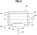
- FIG. 3 is a schematic diagram of a dry etching apparatus (the same applied to the following dry etchings) used for the dry etching.
- the dry etching apparatus 100 includes a chamber 101, grounds 102, a lower electrode 103, an antenna coil 104, and high frequency power sources RF1 and RF2.
- a substrate to be treated (a substrates with films for evaluation) 105 is placed on the lower electrode 103.
- the dry etching was carried out by an etching apparatus shown in FIG. 3 under the following conditions.
- emission spectrum from plasma was measured by an optical emission spectrometer (OES) equipped in the etching apparatus, an intensity of emitted light derived from nitrogen (N) was monitored, and the point when the intensity of emitted light derived from nitrogen (N) started to decrease was automatically detected as an end point.
- OES optical emission spectrometer
- a 20 % of the time (t) from the start of etching to the end point was added as an over-etching time to the time (t), and the time corresponding to 120% of the time (t) was set as a treating time.
- the treating time is shown in Table 1.
- the dry etching was carried out by an etching apparatus shown in FIG. 3 under the following conditions.
- SPM sulfuric acid-hydrogen peroxide mixture
- Table 1 T Thickness Protection film Absorber film Treating time [second] Film thickness after treatment [nm] T all [nm] First layer Second layer Third layer T all : Total thickness TaO or Ta layer TaN layer TaON layer Composition (atomic ratio) T [nm] Composition (atomic ratio) T [nm] Composition (atomic ratio) T [nm] Composition (atomic ratio) T [nm] Treatment (ii) (i) (ii) (iii) Experimental Example 1 RuNb (82:12) 3.9 60.0 TaO (70:30) 1.0 TaN (57:43) 58.5 TaON (40:30:30) 1.0 143 3.8 3.8 3.1 Experimental Example 2 RuNb (82:12) 3.9 60.0 TaO (80:20) 1.5 TaN (57:43) 57.5 TaON (40:30:30) 1.0 140 4.2 4.2 3.9 Experimental Example 3 RuNb (82:12) 3.9 60.0 Ta 1.5 TaN (57:43) 57.5 TaON (40:30:30)
- the thicknesses of the protection films after the treatment (i) were decreased in the substrates with films for evaluation not including the first layer (Comparative Experimental Examples 1 and 2). On the other hand, in the substrates with films for evaluation including the first layer (Experimental Examples 1 to 4), the thicknesses of the protection films after the treatment (i) remained at almost the same thicknesses as the formed thicknesses.
- the treating times of treatment (i) of the substrates with films for evaluation including the TaO layer as the first layer of the absorber film were long compared to those of the substrates with films for evaluation not including the first layer (Comparative Experimental Examples 1 and 2). It is considered that since nitrogen (N) diffused from the TaN layer to form a TaON layer at the interface portion between the TaO layer and the TaN layer, the detection of the end point of etching was delayed.
Landscapes
- Physics & Mathematics (AREA)
- General Physics & Mathematics (AREA)
- Preparing Plates And Mask In Photomechanical Process (AREA)
- Exposure Of Semiconductors, Excluding Electron Or Ion Beam Exposure (AREA)
Applications Claiming Priority (1)
| Application Number | Priority Date | Filing Date | Title |
|---|---|---|---|
| JP2023060853 | 2023-04-04 |
Publications (2)
| Publication Number | Publication Date |
|---|---|
| EP4443235A2 true EP4443235A2 (de) | 2024-10-09 |
| EP4443235A3 EP4443235A3 (de) | 2025-01-08 |
Family
ID=90368743
Family Applications (1)
| Application Number | Title | Priority Date | Filing Date |
|---|---|---|---|
| EP24164620.7A Pending EP4443235A3 (de) | 2023-04-04 | 2024-03-19 | Reflektierender maskenrohling und herstellungsverfahren für reflektierende maske |
Country Status (6)
| Country | Link |
|---|---|
| US (1) | US20240337916A1 (de) |
| EP (1) | EP4443235A3 (de) |
| JP (1) | JP2024148148A (de) |
| KR (1) | KR20240148734A (de) |
| CN (1) | CN118778342A (de) |
| TW (1) | TW202501141A (de) |
Citations (2)
| Publication number | Priority date | Publication date | Assignee | Title |
|---|---|---|---|---|
| JP2002122981A (ja) | 2000-10-13 | 2002-04-26 | Samsung Electronics Co Ltd | 反射型フォトマスク |
| JP2002246299A (ja) | 2001-02-20 | 2002-08-30 | Oki Electric Ind Co Ltd | 反射型露光マスク、反射型露光マスクの製造方法、及び半導体素子 |
Family Cites Families (4)
| Publication number | Priority date | Publication date | Assignee | Title |
|---|---|---|---|---|
| US9285673B2 (en) * | 2014-07-10 | 2016-03-15 | Taiwan Semiconductor Manufacturing Company, Ltd. | Assist feature for a photolithographic process |
| US12001132B2 (en) * | 2018-08-17 | 2024-06-04 | Taiwan Semiconductor Manufacturing Company, Ltd. | Protection layer on low thermal expansion material (LTEM) substrate of extreme ultraviolet (EUV) mask |
| KR102285099B1 (ko) * | 2020-01-08 | 2021-08-04 | 주식회사 에스앤에스텍 | 극자외선용 반사형 블랭크 마스크 및 포토마스크 |
| US11221554B2 (en) * | 2020-01-17 | 2022-01-11 | Taiwan Semiconductor Manufacturing Co., Ltd. | EUV masks to prevent carbon contamination |
-
2024
- 2024-03-08 JP JP2024035715A patent/JP2024148148A/ja active Pending
- 2024-03-19 EP EP24164620.7A patent/EP4443235A3/de active Pending
- 2024-03-26 US US18/616,797 patent/US20240337916A1/en active Pending
- 2024-03-28 KR KR1020240042163A patent/KR20240148734A/ko active Pending
- 2024-04-02 CN CN202410393516.0A patent/CN118778342A/zh active Pending
- 2024-04-02 TW TW113112456A patent/TW202501141A/zh unknown
Patent Citations (2)
| Publication number | Priority date | Publication date | Assignee | Title |
|---|---|---|---|---|
| JP2002122981A (ja) | 2000-10-13 | 2002-04-26 | Samsung Electronics Co Ltd | 反射型フォトマスク |
| JP2002246299A (ja) | 2001-02-20 | 2002-08-30 | Oki Electric Ind Co Ltd | 反射型露光マスク、反射型露光マスクの製造方法、及び半導体素子 |
Also Published As
| Publication number | Publication date |
|---|---|
| EP4443235A3 (de) | 2025-01-08 |
| CN118778342A (zh) | 2024-10-15 |
| TW202501141A (zh) | 2025-01-01 |
| US20240337916A1 (en) | 2024-10-10 |
| JP2024148148A (ja) | 2024-10-17 |
| KR20240148734A (ko) | 2024-10-11 |
Similar Documents
| Publication | Publication Date | Title |
|---|---|---|
| JP5696666B2 (ja) | Euvリソグラフィ用光学部材およびeuvリソグラフィ用反射層付基板の製造方法 | |
| KR20120106735A (ko) | Euv 리소그래피용 반사층이 형성된 기판, euv 리소그래피용 반사형 마스크 블랭크, euv 리소그래피용 반사형 마스크, 및 그 반사층이 형성된 기판의 제조 방법 | |
| US12050396B2 (en) | Reflective mask blank, method of manufacturing thereof, and reflective mask | |
| US12474628B2 (en) | Reflective mask blank and method for manufacturing reflective mask | |
| US11860529B2 (en) | Substrate with multilayer reflection film for EUV mask blank, manufacturing method thereof, and EUV mask blank | |
| EP4443235A2 (de) | Reflektierender maskenrohling und herstellungsverfahren für reflektierende maske | |
| US12124162B2 (en) | Substrate with film for reflective mask blank, reflective mask blank, and method for manufacturing reflective mask | |
| US20240210813A1 (en) | Reflective Mask Blank, Reflective Mask, and Manufacturing Method Thereof | |
| US20250060658A1 (en) | Reflective mask blank and manufacturing method of reflective mask | |
| US20250102898A1 (en) | Reflective mask blank and manufacturing method of reflective mask | |
| US20250060659A1 (en) | Reflective mask blank and manufacturing method of reflective mask | |
| EP4390537A2 (de) | Reflektierender maskenrohling | |
| US12265321B2 (en) | Reflective mask blank, and method for manufacturing reflective mask | |
| US20260050206A1 (en) | Reflective mask blank | |
| EP4546046A2 (de) | Reflektierender fotomaskenrohling und verfahren zur herstellung einer reflektierenden fotomaske | |
| US20250172862A1 (en) | Reflective mask blank and manufacturing method thereof | |
| JP2025051606A (ja) | 反射型マスクブランク、及び反射型マスクの製造方法 |
Legal Events
| Date | Code | Title | Description |
|---|---|---|---|
| PUAI | Public reference made under article 153(3) epc to a published international application that has entered the european phase |
Free format text: ORIGINAL CODE: 0009012 |
|
| STAA | Information on the status of an ep patent application or granted ep patent |
Free format text: STATUS: THE APPLICATION HAS BEEN PUBLISHED |
|
| AK | Designated contracting states |
Kind code of ref document: A2 Designated state(s): AL AT BE BG CH CY CZ DE DK EE ES FI FR GB GR HR HU IE IS IT LI LT LU LV MC ME MK MT NL NO PL PT RO RS SE SI SK SM TR |
|
| PUAL | Search report despatched |
Free format text: ORIGINAL CODE: 0009013 |
|
| AK | Designated contracting states |
Kind code of ref document: A3 Designated state(s): AL AT BE BG CH CY CZ DE DK EE ES FI FR GB GR HR HU IE IS IT LI LT LU LV MC ME MK MT NL NO PL PT RO RS SE SI SK SM TR |
|
| RIC1 | Information provided on ipc code assigned before grant |
Ipc: G03F 1/58 20120101ALI20241203BHEP Ipc: G03F 1/48 20120101ALI20241203BHEP Ipc: G03F 1/24 20120101AFI20241203BHEP |
|
| STAA | Information on the status of an ep patent application or granted ep patent |
Free format text: STATUS: REQUEST FOR EXAMINATION WAS MADE |
|
| 17P | Request for examination filed |
Effective date: 20250130 |