EP4440251A1 - Circuit board assembly and electronic device - Google Patents
Circuit board assembly and electronic device Download PDFInfo
- Publication number
- EP4440251A1 EP4440251A1 EP23869730.4A EP23869730A EP4440251A1 EP 4440251 A1 EP4440251 A1 EP 4440251A1 EP 23869730 A EP23869730 A EP 23869730A EP 4440251 A1 EP4440251 A1 EP 4440251A1
- Authority
- EP
- European Patent Office
- Prior art keywords
- circuit board
- conductive structure
- shielding cover
- board assembly
- recess
- Prior art date
- Legal status (The legal status is an assumption and is not a legal conclusion. Google has not performed a legal analysis and makes no representation as to the accuracy of the status listed.)
- Pending
Links
Images




Classifications
-
- H—ELECTRICITY
- H05—ELECTRIC TECHNIQUES NOT OTHERWISE PROVIDED FOR
- H05K—PRINTED CIRCUITS; CASINGS OR CONSTRUCTIONAL DETAILS OF ELECTRIC APPARATUS; MANUFACTURE OF ASSEMBLAGES OF ELECTRICAL COMPONENTS
- H05K1/00—Printed circuits
- H05K1/02—Details
-
- H—ELECTRICITY
- H05—ELECTRIC TECHNIQUES NOT OTHERWISE PROVIDED FOR
- H05K—PRINTED CIRCUITS; CASINGS OR CONSTRUCTIONAL DETAILS OF ELECTRIC APPARATUS; MANUFACTURE OF ASSEMBLAGES OF ELECTRICAL COMPONENTS
- H05K9/00—Screening of apparatus or components against electric or magnetic fields
- H05K9/0007—Casings
- H05K9/002—Casings with localised screening
- H05K9/0022—Casings with localised screening of components mounted on printed circuit boards [PCB]
- H05K9/0024—Shield cases mounted on a PCB, e.g. cans or caps or conformal shields
-
- H—ELECTRICITY
- H05—ELECTRIC TECHNIQUES NOT OTHERWISE PROVIDED FOR
- H05K—PRINTED CIRCUITS; CASINGS OR CONSTRUCTIONAL DETAILS OF ELECTRIC APPARATUS; MANUFACTURE OF ASSEMBLAGES OF ELECTRICAL COMPONENTS
- H05K1/00—Printed circuits
- H05K1/02—Details
- H05K1/11—Printed elements for providing electric connections to or between printed circuits
-
- H—ELECTRICITY
- H05—ELECTRIC TECHNIQUES NOT OTHERWISE PROVIDED FOR
- H05K—PRINTED CIRCUITS; CASINGS OR CONSTRUCTIONAL DETAILS OF ELECTRIC APPARATUS; MANUFACTURE OF ASSEMBLAGES OF ELECTRICAL COMPONENTS
- H05K9/00—Screening of apparatus or components against electric or magnetic fields
- H05K9/0007—Casings
- H05K9/002—Casings with localised screening
- H05K9/0022—Casings with localised screening of components mounted on printed circuit boards [PCB]
- H05K9/0024—Shield cases mounted on a PCB, e.g. cans or caps or conformal shields
- H05K9/0026—Shield cases mounted on a PCB, e.g. cans or caps or conformal shields integrally formed from metal sheet
- H05K9/0028—Shield cases mounted on a PCB, e.g. cans or caps or conformal shields integrally formed from metal sheet with retainers or specific soldering features
Definitions
- This application relates to the field of electronic device technologies, and in particular, to a circuit board assembly and an electronic device.
- a device layout of a circuit board shows a development trend of high density.
- the device layout of the circuit board there is a scenario in which a shielding cover and a chip are disposed back-to-back.
- this arrangement may lead to poor maintainability of the circuit board and reduce operating reliability of the circuit board.
- Embodiments of this application provide a circuit board assembly and an electronic device, and can improve maintainability and reliability of a circuit board based on ensuring that a shielding cover has good operating reliability.
- this application provides a circuit board assembly.
- the circuit board assembly includes:
- the recess is provided in a part where the conductive cover is attached to the chip back-to-back, and the conductive structure is located in the recess and connected between the conductive cover and the circuit board.
- the conductive structure may be located at a position where the shielding cover is attached to the chip back-to-back, so that when the shielding cover is repaired, the shielding cover may not be directly attached to the chip back-to-back due to a presence of the conductive structure.
- the shielding cover is repaired, there is no need to heat the part where the shielding cover is attached to the chip back-to-back, so that the chip may not be directly heated, and the risk of the adhesive explosion of the chip is low.
- the conductive structure may be located at the position where the shielding cover is attached to the chip back-to-back, and the conductive structure is attached to the chip back-to-back due to the presence of the conductive structure.
- a stress on the shielding cover during the maintenance operation can be absorbed by the conductive structure and a stress on the solder joint of the chip is reduced.
- a part of the structure of the shielding cover is replaced with the conductive structure, still ensuring a shielding effect and performance of the shielding cover, and the maintainability and operating reliability of the circuit board assembly are better.
- the conductive structure includes a compressed state and a natural state.
- the conductive structure When the conductive structure is in the compressed state, the conductive structure is connected between the shielding cover and the circuit board.
- the conductive structure When the conductive structure is in the natural state, the conductive structure is connected to the shielding cover and separated from the circuit board, or the conductive structure is connected to the circuit board and separated from the shielding cover.
- the conductive structure when the conductive structure is in the natural state, the conductive structure may be connected to the shielding cover and separated from the circuit board, so that the shielding cover and the conductive structure are combined together and fed as a whole, so as to be connected together to a first solder pad on the first surface.
- the conductive structure may be connected to the top wall of the recess.
- the conductive structure may be adhered on the top wall of the recess.
- the conductive structure when the conductive structure is in the natural state, the conductive structure may be connected to the circuit board and separated from the shielding cover, so that the conductive structure and the shielding cover are two parts and are respectively connected to the first solder pad on the first surface.
- the conductive structure may be welded or adhered to the first solder pad of the circuit board.
- the conductive structure When the conductive structure is in the compressed state, the conductive structure is connected between the shielding cover and the circuit board. Specifically, the conductive structure is connected between the top wall of the recess and the first solder pad. For example, the conductive structure is adhered on the top wall of the recess and welded to the first solder pad. Specifically, the conductive structure may be welded to the first solder pad of the circuit board first, and then the shielding cover is welded to the circuit board. Alternatively, the conductive structure may be adhered to the recess of the shielding cover first, and then the shielding cover with the conductive structure adhered is welded to the first solder pad of the circuit board.
- the conductive structure may be in contact with the flange of the shielding cover.
- an auxiliary structure may also be added and pressed against the main body of the shielding cover to avoid a problem of false welding caused by expansion of the conductive structure.
- the recess includes the top wall, a first side wall, and a second side wall, the top wall is connected between the first side wall and the second side wall, the conductive structure is in contact with the top wall, and the conductive structure is spaced apart from both the first side wall and the second side wall.
- the conductive structure is spaced apart from both the first side wall and the second side wall, and a gap may be left so that the gap may be used as expansion space for the conductive structure to expand, thereby effectively avoiding the problem of false welding between the shielding cover and the circuit board due to the expansion of the conductive structure, and achieving good reliability.
- distances/a distance between the conductive structure and the first side wall and/or the second side wall are/is in a range from 0.2 mm to 0.5 mm.
- the first solder pad is disposed on the first surface, and the first solder pad is in contact with the conductive structure, or the first solder pad and the conductive structure are connected via a solder material. Therefore, a mounting manner of the conductive structure may be flexibly selected according to different application scenarios.
- the first solder pad is in contact with the conductive structure, and the conductive structure is configured to be pressed against the first solder pad by an external structural member located on a side of the flange facing away from the circuit board.
- the conductive structure electrically connects the circuit board and the shielding cover under a pressure exerted by the external structural member, thereby achieving the shielding effect and performance of the shielding cover.
- the part where the shielding cover is attached to the chip back-to-back is not welded with a soldering material, there is no need to heat the first solder pad and a second solder pad of the corresponding parts of the chip when the shielding cover is repaired, so that the chip may not be directly heated, and the risk of adhesive explosion of the chip is low.
- the stress on the shielding cover is absorbed by the conductive structure, and the stress on the solder joint of the chip is reduced.
- the circuit board assembly further includes an electronic component, the electronic component is disposed on the first surface and is located in the accommodation space, and the conductive structure is spaced apart from the electronic component.
- a spacing between the conductive structure and the electronic component is in a range from 0.3 mm to 0.5 mm.
- a length of the conductive structure is less than or equal to a length of the main body.
- a part or almost all of one edge of the flange may be replaced with a conductive structure according to needs of application scenarios, and other edges of the flange are still made of a material of the shielding cover.
- the conductive structure includes a plurality of substructures, the plurality of substructures are spaced apart from each other, each substructure is connected between the top wall of the recess and the first surface, and a distance between two adjacent substructures is less than or equal to 1.2 mm.
- the conductive structure may be designed into a plurality of small sections to fully consider a spacing between two adjacent first solder pads and a requirement for electromagnetic shielding, to facilitate further expanding a size of the shielding cover.
- a problem of poor welding between the shielding cover and the first solder pad can be resolved, coplanarity between the shielding cover and the first solder pad can be ensured, and a thickness of the circuit board assembly can be reduced to a certain extent.
- a type of the conductive structure includes one of or a combination of a conductive pad, conductive foam, and conductive fabric.
- a width of the recess is in a range from 0.6 mm to 1.5 mm, and a height of the recess is in a range from 0.2 mm to 0.75 mm.
- a width of the conductive structure is in a range from 0.6 mm to 1.5 mm, and a height of the conductive structure is in a range from 0.6 mm to 1.7 mm.
- this application provides an electronic device.
- the electronic device includes a housing and the foregoing circuit board assembly.
- the circuit board assembly is accommodated in the housing.
- a and/or B may represent the following three cases: only A exists, both A and B exist, and only B exists.
- a plurality of: It means "two or more”.
- A is connected to B, A may be directly connected to B, or A and B may be indirectly connected via an intermediate medium.
- Embodiments of this application provide a circuit board assembly and an electronic device.
- the electronic device may be but is not limited to a device such as a mobile phone, a tablet computer, an e-reader, a notebook computer, an in-vehicle device, a wearable device, or a wireless microwave receiving device.
- a mobile phone an electronic device that is widely used by a user in various application scenarios is used as an example for descriptions, but it may be understood that the mobile phone does not constitute a limitation.
- FIG. 1 is a schematic diagram of a structure of an electronic device 200 according to an embodiment of this application
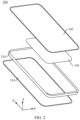
- FIG. 2 is a schematic exploded view of the electronic device 200 shown in FIG. 1 .
- a length direction of the electronic device 200 is a first direction X
- a width direction of the electronic device 200 is a second direction Y
- a height direction of the electronic device 200 is a third direction Z
- the first direction X, the second direction Y, and the third direction Z are perpendicular to each other.
- the electronic device 200 may include a housing 210 and a circuit board assembly 100.
- the circuit board assembly 100 is accommodated inside the housing 210 and can be protected from damage caused by external mechanical damage under protection of the housing 210.
- the housing 210 may include a display module 220, a frame 230, and a rear cover 240.
- the display module 220 and the rear cover 240 are respectively connected to opposite sides of the frame 230.
- the display module 220 may be configured to display a text, an image, a video, and the like.
- the frame 230 serves as a structural bearing member of the electronic device 200 and is configured to mount the display module 220, the rear cover 240, and another component.
- the frame 230 is a middle frame of the mobile phone
- the display module 220 is a cover plate facing the face of a user when the user holds the mobile phone.
- the display module 220 may be provided with a display screen to present an image, color, a text, and other visual information.
- the rear cover 240 is a cover plate facing away from the face of a user when the user holds the mobile phone.
- the rear cover 240 may be provided with a camera module as a rear camera to capture a still image or a dynamic video behind the mobile phone.
- a material of the rear cover 240 includes glass, plastic, or ceramic.
- the display module 220, the rear cover 240, and the frame 230 cooperate to define accommodating space of the electronic device 200.
- the accommodating space may accommodate the circuit board assembly 100, a battery, the camera module, and another component.
- the circuit board assembly 100 is located in the accommodating space.
- the circuit board assembly 100 is located between the frame 230 and the rear cover 240.
- the circuit board assembly 100 may be fixed to the frame 230, or the circuit board assembly 100 may be fixed to the rear cover 240.
- FIG. 3 is a schematic top view of the circuit board assembly 100 shown in FIG. 2
- FIG. 4 is a schematic sectional view obtained by cutting along an A-A sectional line shown in FIG. 3 .
- the circuit board assembly 100 may include a circuit board 10, a chip 20, an electronic component 30, and a shielding cover 40.
- the electronic component 30 is disposed on the circuit board 10, and the shielding cover 40 covers a periphery of the electronic component 30 and is connected to the circuit board 10.
- the chip 20 is connected to the circuit board 10, and the chip 20 and the shielding cover 40 is respectively located on opposite sides of the circuit board 10. In other words, the chip 20 and the shielding cover 40 are disposed back-to-back.
- the circuit board 10 may be, but is not limited to, a printed circuit board, a flexible circuit board, or a rigid-flexible circuit board.
- the electronic component 30 may be a chip such as a CPU (Central Processing Unit, central processing unit), a GPU (Graphic Processing Unit, graphic processing unit), a TPU (Tensor Processing Unit, tensor processing unit), an AP (Application Processor, application processor), and an RFPA (Radio Frequency Power Amplifier, radio frequency power amplifier).
- a CPU Central Processing Unit, central processing unit
- a GPU Graphic Processing Unit, graphic processing unit
- TPU Torsor Processing Unit, tensor processing unit
- AP Application Processor
- RFPA Radio Frequency Power Amplifier, radio frequency power amplifier
- the circuit board 10 may include a first surface 11 and a second surface 12 that are disposed opposite to each other.
- the electronic component 30 and the shielding cover 40 may be disposed on the first surface 11.
- a plurality of first solder pads 13 are disposed on the first surface 11, and the plurality of first solder pads 13 are spaced apart from each other.
- a first solder pad 13 may be a functional solder pad to achieve an electrical connection effect.
- the first solder pad 13 may be configured to be electrically connected to the electronic component 30 or the shielding cover 40.
- a first solder pad 13 may be a non-functional solder pad to achieve an effect in mechanical fixing, support, and the like.
- the chip 20 may be disposed on the second surface 12.
- a plurality of second solder pads 14 are disposed on the second surface 12, and the plurality of second solder pads 14 are spaced apart from each other.
- a second solder pad 14 may be a functional solder pad to achieve an electrical connection effect.
- the second solder pad 14 may be configured to be electrically connected to the chip 20.
- a second solder pad 14 may alternatively be a non-functional solder pad to achieve an effect in mechanical fixing, support, and the like. The following describes an example in which the first solder pad 13 and the second solder pad 14 are functional pads.
- the plurality of second solder pads 14 and the plurality of first solder pads 13 at least partially overlap in a height direction of the circuit board 10 (that is, the third direction Z). In this way, a solder pad of the shielding cover 40 and a solder pad of the chip 20 may be directly disposed back-to-back, so that the shielding cover 40 and the chip 20 can be disposed back-to-back.
- the electronic component 30 is disposed on the first surface 11, and the shielding cover 40 is also disposed on the first surface 11 and covers the periphery of the electronic component 30.
- the chip 20 is disposed on the second surface 12, and the chip 20 may be a chip 20 with a BGA (Ball Grid Array, ball grid array) solder ball 21. It may be understood that the electronic component 30 is a source of electromagnetic interference (electromagnetic interference, EMI).
- the shielding cover 40 is disposed at the periphery of the electronic component 30 to cover the electronic component 30, so that electromagnetic interference of the electronic component 30 can be shielded, thereby achieving good electromagnetic shielding performance and facilitating working performance of the electronic device 200.
- a component disposed on the circuit board 10 are not limited to the foregoing component.
- the component may alternatively be another component such as a capacitor, an inductor, or a heat sink that can achieve functions such as electrical connection, protection, support, heat dissipation, and assembly.
- There may be one or more electronic components 30 and shielding covers 40 as needed. The following only uses a structure of one shielding cover 40 as an example to describe a structure of the shielding cover 40 in detail. Any improvement in the structure of one shielding cover 40 may be applied to another shielding cover 40 in a case of no conflict.
- FIG. 5 is a schematic sectional view obtained by cutting along a B-B sectional line shown in FIG. 3
- FIG. 6 is a schematic sectional view obtained by cutting along a C-C sectional line shown in FIG. 3 .
- the shielding cover 40 includes a main body 41 and a flange 42.
- the main body 41 is in a shape of an inverted frame, and the main body 41 defines accommodation space 411.
- the accommodation space 411 may provide accommodating space for the electronic component 30 and electromagnetic shielding space for the electronic component 30.
- the flange 42 is connected to one end of the main body 41 in a peripheral direction of the main body 41, and an angle is formed between the flange 42 and the main body 41.
- the angle between the flange 42 and the main body 41 may be selected arbitrarily based on satisfying operating reliability of the shielding cover 40. This is not strictly limited in embodiments of this application.
- the angle between the flange 42 and the main body 41 may be 90° (falling within an allowable tolerance range).
- the flange 42 is also connected to the first surface 11 of the circuit board 10. Specifically, the flange 42 may be connected to the first solder pad 13 disposed on the first surface 11.
- the flange 42 is disposed to provide a sufficient contact area between the shielding cover 40 and the circuit board 10, to achieve a good fixing effect.
- the flange 42 may include two first side edges 421 and two second side edges 422.
- the two first side edges 421 are arranged opposite to each other in the first direction X
- the two second side edges 422 are arranged opposite to each other in the second direction Y.
- the two second side edges 422 are connected between the two first side edges 421.
- a recess 423 is provided on a surface of the flange 42 facing the first surface 11.
- the recess 423 runs through the flange 42 in a width direction of the flange 42 (that is, the second direction Y) and is communicated with the accommodation space 411.
- the recess 423 may be located on any one, two, three, or four of the two first side edges 421 and the two second side edges 422.
- the plurality of recesses 423 are spaced apart from each other.
- the following uses only one recess 423 and the recess 423 being located on one second side edge 422 of the two second side edges 422 as an example to describe a structure of the recess 423 in detail. Any improvement in a structure of one second side edge 422 of the two second side edges 422 may be applied to another edge of the flange 42 in a case of no conflict.
- the recess 423 is provided on one second side edge 422 of the two second side edges 422, and orthographic projection of the recess 423 on the circuit board 10 at least partially falls within an orthographic projection range of the chip 20 on the circuit board 10.
- the recess 423 may include a top wall 424, a first side wall 425, and a second side wall 426.
- the top wall 424 is a wall in the recess 423 that is disposed opposite to the first surface 11 of the circuit board 10.
- the first side wall 425 and the second side wall 426 are disposed opposite to each other.
- the top wall 424 is connected between the first side wall 425 and the second side wall 426.
- a width of the recess 423 may be in a range from 0.6 mm to 1.5 mm (including end values 0.6 mm and 1.5 mm), and the width of the recess 423 is a size of the recess 423 in the second direction Y.
- a height of the recess 423 may be in a range from 0.2 mm to 0.75 mm (including end values 0.2 mm and 0.75 mm), and the height of the recess 423 is a size of the recess 423 in the third direction Z.
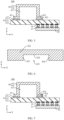
- FIG. 7 is another schematic sectional view obtained by cutting along a B-B sectional line shown in FIG. 3
- FIG. 8 is another schematic sectional view obtained by cutting along a C-C sectional line shown in FIG. 3
- the circuit board assembly 100 may further include a conductive structure 50.
- the conductive structure 50 is located in the recess 423 and connected between the top wall 424 of the recess 423 and the first surface 11. Orthographic projection of the conductive structure 50 on the circuit board 10 at least partially falls within the orthographic projection range of the chip 20 on the circuit board 10.
- the conductive structure 50 may be connected between the flange 42 and the first solder pad 13 to implement physical and electrical connections between the shielding cover 40 and the circuit board 10 via the conductive structure 50.
- the recess 423 is provided in a part where the conductive cover is attached to the chip 20 back-to-back, and the conductive structure 50 is located in the recess 423 and connected between the conductive cover and the circuit board 10.
- the conductive structure 50 may be located at a position where the shielding cover 40 is attached to the chip 20 back-to-back, so that when the shielding cover 40 is repaired, the shielding cover 40 may not be directly attached to the chip 20 back-to-back due to a presence of the conductive structure 50.
- the shielding cover 40 is repaired, there is no need to heat the part where the shielding cover 40 is attached to the chip 20 back-to-back, so that the chip 20 may not be directly heated, and the risk of the adhesive explosion of the chip 20 is low.
- the conductive structure 50 may be located at the position where the shielding cover 40 is attached to the chip 20 back-to-back, and the conductive structure 50 is attached to the chip 20 back-to-back due to the presence of the conductive structure 50.
- a stress on the shielding cover 40 during the maintenance operation can be absorbed by the conductive structure 50 and a stress on the solder joint of the chip 20 is reduced.
- a part of the structure of the shielding cover 40 is replaced with the conductive structure 50, still ensuring a shielding effect and performance of the shielding cover 40, and the maintainability and operating reliability of the circuit board assembly 100 are better.
- the conductive structure 50 is a conductive material having compression performance.
- a type of the conductive structure 50 includes one of or a combination of a conductive pad, conductive foam, and conductive fabric.
- a compression amount of the conductive structure 50 may be around 50% (falling within an allowable tolerance range).
- a width of the conductive structure 50 may be in a range from 0.6 mm to 1.5 mm (including end values 0.6 mm and 1.5 mm), and the width of the conductive structure 50 is a size of the conductive structure 50 in the second direction Y.
- a height of the conductive structure 50 may be in a range from 0.6 mm to 1.7 mm (including end values 0.6 mm and 1.7 mm), and the height of the conductive structure 50 is a size of the conductive structure 50 in the third direction Z. It should be understood that the width and height of the conductive structure 50 may be related to the width and height of the recess 423.
- the width of the conductive structure 50 may be the same as the width of the recess 423 and is also W mm, and the height of the conductive structure 50 may be 2H+0.2 mm.
- the conductive structure 50 may include a compressed state and a natural state.
- the conductive structure 50 When the conductive structure 50 is in the natural state, the conductive structure 50 may be connected to the shielding cover 40 and separated from the circuit board 10, so that the shielding cover 40 and the conductive structure 50 are combined together and fed as a whole, so as to be connected together to the first solder pad 13 on the first surface 11.
- the conductive structure 50 may be connected to the top wall 424 of the recess 423.
- the conductive structure 50 may be adhered on the top wall 424 of the recess 423.
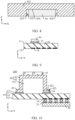
- FIG. 9 is a schematic assembly diagram of the conductive structure 50 and the first solder pad 13 shown in FIG. 7 .
- the conductive structure 50 may be connected to the circuit board 10 and separated from the shielding cover 40, so that the conductive structure 50 and the shielding cover 40 are two parts and are respectively connected to the first solder pads 13 on the first surface 11.
- the conductive structure 50 may be welded or adhered to the first solder pad 13 of the circuit board 10.
- FIG. 10 is a schematic diagram of states of the conductive structure 50, the first solder pad 13, and the shielding cover 40 shown in FIG. 7 during a reflow soldering process.
- the conductive structure 50 may be welded to the first solder pad 13 of the circuit board 10 first, and then the shielding cover 40 is welded to the circuit board 10.
- the conductive structure 50 may be adhered to the recess 423 of the shielding cover 40 first, and then the shielding cover 40 with the conductive structure 50 adhered is welded to the first solder pad 13 of the circuit board 10.
- the conductive structure 50 may be in contact via the flange 42 of the shielding cover 40.
- an auxiliary structure 61 may also be added and pressed against the main body 41 of the shielding cover 40 to avoid a problem of false welding caused by expansion of the conductive structure 50.
- the conductive structure 50 When the conductive structure 50 is connected between the shielding cover 40 and the circuit board 10, the conductive structure 50 is located in the recess 423. The conductive structure 50 is in contact with the top wall 424 of the recess 423 and the first solder pad 13. Both ends of the conductive structure 50 are spaced apart from the first side wall 425 of the recess 423 and the second side wall 426 of the recess 423 respectively.
- the conductive structure 50 is spaced apart from both the first side wall 425 and the second side wall 426, and a gap may be left so that the gap may be used as expansion space for the conductive structure 50 to expand, thereby effectively avoiding the problem of false welding between the shielding cover 40 and the circuit board 10 due to the expansion of the conductive structure 50, and achieving good reliability.
- distances/a distance between the conductive structure 50 and the first side wall 425 and/or the second side wall 426 are/is in a range from 0.2 mm to 0.5 mm (including end values 0.2 mm and 0.5 mm).
- the conductive structure 50 may be a structure with six sides wrapped by a conductive material.
- the conductive structure 50 may be a structure in which two opposite end surfaces are not wrapped by a conductive material, and a peripheral side connected between the two end surfaces is wrapped by a conductive material. In this way, the two end surfaces of the conductive structure 50 that are not wrapped by the conductive material may be disposed opposite to the first side wall 425 and the second side wall 426 respectively.
- a part of the shielding cover 40 with the recess 423 and the conductive structure 50 may be the same as a part of the shielding cover 40 without the recess 423 and the conductive structure 50, and both use a soldering material to weld the conductive structure 50 to the first solder pad 13 on the first surface 11.
- the soldering material may be solder.
- the part of the shielding cover 40 without the recess 423 and the conductive structure 50 may use the soldering material, so that the flange 42 is welded to the first solder pad 13 on the first surface 11.
- the part of the shielding cover 40 with the recess 423 and the conductive structure 50 may not use the soldering material, but the conductive structure 50 is in contact with the first solder pad 13 on the first surface 11, and the conductive structure 50 is pressed against the first solder pad 13 by an external structural member located on a side of the flange 42 facing away from the circuit board 10.
- the conductive structure 50 electrically connects the circuit board 10 and the shielding cover 40 under a pressure exerted by the external structural member, thereby achieving the shielding effect and performance of the shielding cover 40.
- the part where the shielding cover 40 is attached to the chip 20 back-to-back is not welded with a soldering material, there is no need to heat the first solder pad 13 and the second solder pad 14 of corresponding parts of the chip 20 when the shielding cover 40 is repaired, so that the chip 20 may not be directly heated, and the risk of adhesive explosion of the chip 20 is low.
- the stress on the shielding cover 40 is absorbed by the conductive structure 50, and the stress on the solder joint of the chip 20 is reduced.
- the conductive structure 50 is spaced apart from the electronic component 30. In this way, a short circuit problem caused by collision between the conductive structure 50 and the electronic component 30 located inside the accommodation space 411 can be avoided, and the circuit board assembly 100 has good operating reliability.
- a distance between the conductive structure 50 and the electronic component 30 is in a range from 0.3 mm to 0.5 mm (including end values 0.3 mm and 0.5 mm).
- a length of the recess 423 may be less than a length of the main body 41, and a length of the conductive structure 50 may be less than the length of the main body 41.
- a length is a size in the first direction X. In this way, a part of one edge of the flange 42 may be replaced with the conductive structure 50, and other parts of the edge are still made of a material of the shielding cover 40.
- FIG. 11 is a schematic sectional view obtained by cutting along a D-D sectional line shown in FIG. 3
- FIG. 12 is a schematic side view of the shielding cover 40 shown in FIG. 11
- the top wall 424 of the recess 423 is located on two first side edges 421 and one second side edge 422
- the first side wall 425 of the recess 423 and the second side wall 426 of the recess 423 are respectively located on the two first side edges 421.
- the length of the recess 423 may be equal to the length of the main body 41
- the length of the conductive structure 50 may be equal to the length of the main body 41.
- the length is the size in the first direction X. In this way, almost all of one edge of the flange 42 may be replaced with the conductive structure 50, and other edges of the flange 42 are still made of the material of the shielding cover 40. In addition, the other edges in the flange 42 may be spaced apart from the edge made of the conductive structure 50, to provide the expansion space for the conductive structure 50.
- FIG. 13 is another schematic sectional view obtained by cutting along a C-C sectional line shown in FIG. 3 .
- the conductive structure 50 may include a plurality of substructures 51 the plurality of substructures 51 are spaced apart from each other, and each substructure 51 is connected between the top wall 424 of the recess 423 and the first surface 11.
- the conductive structure 50 may be designed into a plurality of small sections to fully consider a spacing between two adjacent first solder pads 13 and a requirement for electromagnetic shielding, to facilitate further expanding a size of the shielding cover 40.
- a problem of poor welding between the shielding cover 40 and the first solder pad 13 can be resolved, coplanarity between the shielding cover 40 and the first solder pad 13 can be ensured, and a thickness of the circuit board assembly 100 can be reduced to a certain extent.
- a distance between two adjacent substructures 51 is less than or equal to 1.2 mm.
- the flange 42 is an irregular special-shaped flange.
- the conductive structure 50 may include an inner core and a conductive outer layer wrapping the inner core. To match the special-shaped flange, the inner core may be cut without cutting the conductive outer layer, so that the cut inner core and the continuous conductive outer layer can adapt to the special-shaped flange and have bendability. Moreover, based on the bendability, the conductive structure 50 can also be electrically connected between the shielding cover 40 and the circuit board 10 to ensure the shielding effect of the shielding cover 40.
- FIG. 14 is a schematic diagram of a structure of a circuit board assembly 100 according to another embodiment of this application.
- parts of two adjacent shielding covers 40 that are not attached to a chip 20 back-to-back may be welded on a first solder pad 13 first, and parts of the two adjacent shielding covers 40 that are attached to the chip 20 back-to-back may be welded to the first solder pad 13 without using a soldering material.
- a conductive structure 50 may be connected between two adjacent shielding covers 40, and the conductive structure 50, the shielding cover 40, and the first solder pad 13 may be closely connected together via a structural member 62 such as a middle frame or a support, so that the shielding cover 40 can achieve a shielding effect.
Landscapes
- Engineering & Computer Science (AREA)
- Microelectronics & Electronic Packaging (AREA)
- Shielding Devices Or Components To Electric Or Magnetic Fields (AREA)
Abstract
Description
- This application claims priority to
Chinese Patent Application No. 202222603719.7, filed with the China National Intellectual Property Administration on September 28, 2022 - This application relates to the field of electronic device technologies, and in particular, to a circuit board assembly and an electronic device.
- Currently, a device layout of a circuit board shows a development trend of high density. In the device layout of the circuit board, there is a scenario in which a shielding cover and a chip are disposed back-to-back. However, this arrangement may lead to poor maintainability of the circuit board and reduce operating reliability of the circuit board.
- Embodiments of this application provide a circuit board assembly and an electronic device, and can improve maintainability and reliability of a circuit board based on ensuring that a shielding cover has good operating reliability.
- According to a first aspect, this application provides a circuit board assembly. The circuit board assembly includes:
- a circuit board, where the circuit board includes a first surface and a second surface that are disposed opposite to each other;
- a chip, where the chip is disposed on the first surface;
- a shielding cover, where the shielding cover includes a main body and a flange, the main body defines accommodation space, the flange is connected to one end of the main body in a peripheral direction of the main body, an angle is formed between the flange and the main body, the flange is connected to the first surface, a recess is provided on a surface of the flange facing the first surface, and the recess runs through the flange in a width direction of the flange and is communicated with the accommodation space; and
- a conductive structure, where the conductive structure is located in the recess and connected between a top wall of the recess and the first surface, and orthographic projection of the conductive structure on the circuit board at least partially falls within an orthographic projection range of the chip on the circuit board.
- It may be understood that with a development trend of high density of a device layout on the circuit board, there may be a scenario in which the chip and the shielding cover are disposed back-to-back. In this scenario, when it is necessary to perform maintenance operations such as disassembly and welding on the shielding cover for repairing and diagnosing a component in the shielding cover, because the shielding cover is directly attached to the chip back-to-back, problems such as chip failure due to adhesive explosion and increased stress on a solder joint of the chip may easily occur. This further increases a risk of failure of the circuit board assembly and worsens maintainability and operating reliability of the circuit board assembly.
- Therefore, the recess is provided in a part where the conductive cover is attached to the chip back-to-back, and the conductive structure is located in the recess and connected between the conductive cover and the circuit board. The conductive structure may be located at a position where the shielding cover is attached to the chip back-to-back, so that when the shielding cover is repaired, the shielding cover may not be directly attached to the chip back-to-back due to a presence of the conductive structure. When the shielding cover is repaired, there is no need to heat the part where the shielding cover is attached to the chip back-to-back, so that the chip may not be directly heated, and the risk of the adhesive explosion of the chip is low. In addition, the conductive structure may be located at the position where the shielding cover is attached to the chip back-to-back, and the conductive structure is attached to the chip back-to-back due to the presence of the conductive structure. A stress on the shielding cover during the maintenance operation can be absorbed by the conductive structure and a stress on the solder joint of the chip is reduced. Moreover, a part of the structure of the shielding cover is replaced with the conductive structure, still ensuring a shielding effect and performance of the shielding cover, and the maintainability and operating reliability of the circuit board assembly are better.
- In a possible implementation, the conductive structure includes a compressed state and a natural state.
- When the conductive structure is in the compressed state, the conductive structure is connected between the shielding cover and the circuit board.
- When the conductive structure is in the natural state, the conductive structure is connected to the shielding cover and separated from the circuit board, or the conductive structure is connected to the circuit board and separated from the shielding cover.
- It may be understood that when the conductive structure is in the natural state, the conductive structure may be connected to the shielding cover and separated from the circuit board, so that the shielding cover and the conductive structure are combined together and fed as a whole, so as to be connected together to a first solder pad on the first surface. Specifically, the conductive structure may be connected to the top wall of the recess. For example, the conductive structure may be adhered on the top wall of the recess.
- Alternatively, when the conductive structure is in the natural state, the conductive structure may be connected to the circuit board and separated from the shielding cover, so that the conductive structure and the shielding cover are two parts and are respectively connected to the first solder pad on the first surface. For example, the conductive structure may be welded or adhered to the first solder pad of the circuit board.
- When the conductive structure is in the compressed state, the conductive structure is connected between the shielding cover and the circuit board. Specifically, the conductive structure is connected between the top wall of the recess and the first solder pad. For example, the conductive structure is adhered on the top wall of the recess and welded to the first solder pad. Specifically, the conductive structure may be welded to the first solder pad of the circuit board first, and then the shielding cover is welded to the circuit board. Alternatively, the conductive structure may be adhered to the recess of the shielding cover first, and then the shielding cover with the conductive structure adhered is welded to the first solder pad of the circuit board. In both of the foregoing methods, the conductive structure may be in contact with the flange of the shielding cover. During a reflow soldering process, an auxiliary structure may also be added and pressed against the main body of the shielding cover to avoid a problem of false welding caused by expansion of the conductive structure.
- In a possible implementation, the recess includes the top wall, a first side wall, and a second side wall, the top wall is connected between the first side wall and the second side wall, the conductive structure is in contact with the top wall, and the conductive structure is spaced apart from both the first side wall and the second side wall.
- It may be understood that the conductive structure is spaced apart from both the first side wall and the second side wall, and a gap may be left so that the gap may be used as expansion space for the conductive structure to expand, thereby effectively avoiding the problem of false welding between the shielding cover and the circuit board due to the expansion of the conductive structure, and achieving good reliability.
- In a possible implementation, distances/a distance between the conductive structure and the first side wall and/or the second side wall are/is in a range from 0.2 mm to 0.5 mm.
- In a possible implementation, the first solder pad is disposed on the first surface, and the first solder pad is in contact with the conductive structure, or the first solder pad and the conductive structure are connected via a solder material. Therefore, a mounting manner of the conductive structure may be flexibly selected according to different application scenarios.
- In a possible implementation, the first solder pad is in contact with the conductive structure, and the conductive structure is configured to be pressed against the first solder pad by an external structural member located on a side of the flange facing away from the circuit board.
- It may be understood that the conductive structure electrically connects the circuit board and the shielding cover under a pressure exerted by the external structural member, thereby achieving the shielding effect and performance of the shielding cover. In this way, because the part where the shielding cover is attached to the chip back-to-back is not welded with a soldering material, there is no need to heat the first solder pad and a second solder pad of the corresponding parts of the chip when the shielding cover is repaired, so that the chip may not be directly heated, and the risk of adhesive explosion of the chip is low. In addition, the stress on the shielding cover is absorbed by the conductive structure, and the stress on the solder joint of the chip is reduced.
- In a possible implementation, the circuit board assembly further includes an electronic component, the electronic component is disposed on the first surface and is located in the accommodation space, and the conductive structure is spaced apart from the electronic component.
- In this way, a short circuit problem caused by collision between the conductive structure and the electronic component located inside the accommodation space can be avoided, and the circuit board assembly has good operating reliability.
- In a possible implementation, a spacing between the conductive structure and the electronic component is in a range from 0.3 mm to 0.5 mm.
- In a possible embodiment, a length of the conductive structure is less than or equal to a length of the main body.
- In this way, a part or almost all of one edge of the flange may be replaced with a conductive structure according to needs of application scenarios, and other edges of the flange are still made of a material of the shielding cover.
- In a possible embodiment, the conductive structure includes a plurality of substructures, the plurality of substructures are spaced apart from each other, each substructure is connected between the top wall of the recess and the first surface, and a distance between two adjacent substructures is less than or equal to 1.2 mm.
- In this way, the conductive structure may be designed into a plurality of small sections to fully consider a spacing between two adjacent first solder pads and a requirement for electromagnetic shielding, to facilitate further expanding a size of the shielding cover. In addition, based on a contact form in which the shielding cover is in contact with the first solder pad via the substructure, a problem of poor welding between the shielding cover and the first solder pad can be resolved, coplanarity between the shielding cover and the first solder pad can be ensured, and a thickness of the circuit board assembly can be reduced to a certain extent.
- In a possible embodiment, a type of the conductive structure includes one of or a combination of a conductive pad, conductive foam, and conductive fabric.
- In a possible embodiment, a width of the recess is in a range from 0.6 mm to 1.5 mm, and a height of the recess is in a range from 0.2 mm to 0.75 mm.
- In a possible embodiment, a width of the conductive structure is in a range from 0.6 mm to 1.5 mm, and a height of the conductive structure is in a range from 0.6 mm to 1.7 mm.
- According to a second aspect, this application provides an electronic device. The electronic device includes a housing and the foregoing circuit board assembly. The circuit board assembly is accommodated in the housing.
-
-
FIG. 1 is a schematic diagram of a structure of an electronic device according to an embodiment of this application; -
FIG. 2 is a schematic exploded view of the electronic device shown inFIG. 1 ; -
FIG. 3 is a schematic top view of a circuit board assembly shown inFIG. 2 ; -
FIG. 4 is a schematic sectional view obtained by cutting along an A-A sectional line shown inFIG. 3 ; -
FIG. 5 is a schematic sectional view obtained by cutting along a B-B sectional line shown inFIG. 3 ; -
FIG. 6 is a schematic sectional view obtained by cutting along a C-C sectional line shown inFIG. 3 ; -
FIG. 7 is another schematic sectional view obtained by cutting along a B-B sectional line shown inFIG. 3 ; -
FIG. 8 is another schematic sectional view obtained by cutting along a C-C sectional line shown inFIG. 3 ; -
FIG. 9 is a schematic assembly diagram of a conductive structure and a first solder pad shown inFIG. 7 ; -
FIG. 10 is a schematic diagram of states of a conductive structure, a first solder pad, and a shielding cover shown inFIG. 7 during a reflow soldering process; -
FIG. 11 is a schematic sectional view obtained by cutting along a D-D sectional line shown inFIG. 3 ; -
FIG. 12 is a schematic side view of a shielding cover shown inFIG. 11 ; -
FIG. 13 is another schematic sectional view obtained by cutting along a C-C sectional line shown inFIG. 3 ; and -
FIG. 14 is a schematic diagram of a structure of a circuit board assembly according to another embodiment of this application. - For ease of understanding, terms in embodiments of this application are first explained.
- And/or: It is merely an association relationship for describing associated objects and represents that three relationships may exist. For example, A and/or B may represent the following three cases: only A exists, both A and B exist, and only B exists.
- A plurality of: It means "two or more".
- Connection: It should be understood in a broad sense. For example, if A is connected to B, A may be directly connected to B, or A and B may be indirectly connected via an intermediate medium.
- The following clearly describes specific implementations of this application with reference to accompanying drawings.
- Embodiments of this application provide a circuit board assembly and an electronic device. The electronic device may be but is not limited to a device such as a mobile phone, a tablet computer, an e-reader, a notebook computer, an in-vehicle device, a wearable device, or a wireless microwave receiving device.
- A mobile phone, an electronic device that is widely used by a user in various application scenarios is used as an example for descriptions, but it may be understood that the mobile phone does not constitute a limitation.
- Refer to
FIG. 1 andFIG. 2 together.FIG. 1 is a schematic diagram of a structure of anelectronic device 200 according to an embodiment of this application, andFIG. 2 is a schematic exploded view of theelectronic device 200 shown inFIG. 1 . - In this embodiment of this application, for ease of description, a length direction of the
electronic device 200 is a first direction X, a width direction of theelectronic device 200 is a second direction Y, a height direction of theelectronic device 200 is a third direction Z, and the first direction X, the second direction Y, and the third direction Z are perpendicular to each other. Theelectronic device 200 may include ahousing 210 and acircuit board assembly 100. Thecircuit board assembly 100 is accommodated inside thehousing 210 and can be protected from damage caused by external mechanical damage under protection of thehousing 210. - The
housing 210 may include adisplay module 220, aframe 230, and arear cover 240. Thedisplay module 220 and therear cover 240 are respectively connected to opposite sides of theframe 230. Thedisplay module 220 may be configured to display a text, an image, a video, and the like. Theframe 230 serves as a structural bearing member of theelectronic device 200 and is configured to mount thedisplay module 220, therear cover 240, and another component. When theelectronic device 200 is a mobile phone, theframe 230 is a middle frame of the mobile phone, and thedisplay module 220 is a cover plate facing the face of a user when the user holds the mobile phone. In this case, thedisplay module 220 may be provided with a display screen to present an image, color, a text, and other visual information. Therear cover 240 is a cover plate facing away from the face of a user when the user holds the mobile phone. Therear cover 240 may be provided with a camera module as a rear camera to capture a still image or a dynamic video behind the mobile phone. For example, a material of therear cover 240 includes glass, plastic, or ceramic. - The
display module 220, therear cover 240, and theframe 230 cooperate to define accommodating space of theelectronic device 200. The accommodating space may accommodate thecircuit board assembly 100, a battery, the camera module, and another component. Thecircuit board assembly 100 is located in the accommodating space. For example, as shown inFIG. 2 , thecircuit board assembly 100 is located between theframe 230 and therear cover 240. Thecircuit board assembly 100 may be fixed to theframe 230, or thecircuit board assembly 100 may be fixed to therear cover 240. - Refer to
FIG. 3 and FIG. 4 together.FIG. 3 is a schematic top view of thecircuit board assembly 100 shown inFIG. 2 , andFIG. 4 is a schematic sectional view obtained by cutting along an A-A sectional line shown inFIG. 3 . - The
circuit board assembly 100 may include acircuit board 10, achip 20, anelectronic component 30, and a shieldingcover 40. Theelectronic component 30 is disposed on thecircuit board 10, and the shieldingcover 40 covers a periphery of theelectronic component 30 and is connected to thecircuit board 10. Thechip 20 is connected to thecircuit board 10, and thechip 20 and the shieldingcover 40 is respectively located on opposite sides of thecircuit board 10. In other words, thechip 20 and the shieldingcover 40 are disposed back-to-back. Thecircuit board 10 may be, but is not limited to, a printed circuit board, a flexible circuit board, or a rigid-flexible circuit board. Theelectronic component 30 may be a chip such as a CPU (Central Processing Unit, central processing unit), a GPU (Graphic Processing Unit, graphic processing unit), a TPU (Tensor Processing Unit, tensor processing unit), an AP (Application Processor, application processor), and an RFPA (Radio Frequency Power Amplifier, radio frequency power amplifier). - The
circuit board 10 may include afirst surface 11 and asecond surface 12 that are disposed opposite to each other. Theelectronic component 30 and the shieldingcover 40 may be disposed on thefirst surface 11. A plurality offirst solder pads 13 are disposed on thefirst surface 11, and the plurality offirst solder pads 13 are spaced apart from each other. Afirst solder pad 13 may be a functional solder pad to achieve an electrical connection effect. For example, thefirst solder pad 13 may be configured to be electrically connected to theelectronic component 30 or the shieldingcover 40. Alternatively, afirst solder pad 13 may be a non-functional solder pad to achieve an effect in mechanical fixing, support, and the like. Thechip 20 may be disposed on thesecond surface 12. A plurality ofsecond solder pads 14 are disposed on thesecond surface 12, and the plurality ofsecond solder pads 14 are spaced apart from each other. Asecond solder pad 14 may be a functional solder pad to achieve an electrical connection effect. For example, thesecond solder pad 14 may be configured to be electrically connected to thechip 20. Asecond solder pad 14 may alternatively be a non-functional solder pad to achieve an effect in mechanical fixing, support, and the like. The following describes an example in which thefirst solder pad 13 and thesecond solder pad 14 are functional pads. - The plurality of
second solder pads 14 and the plurality offirst solder pads 13 at least partially overlap in a height direction of the circuit board 10 (that is, the third direction Z). In this way, a solder pad of the shieldingcover 40 and a solder pad of thechip 20 may be directly disposed back-to-back, so that the shieldingcover 40 and thechip 20 can be disposed back-to-back. - For example, the
electronic component 30 is disposed on thefirst surface 11, and the shieldingcover 40 is also disposed on thefirst surface 11 and covers the periphery of theelectronic component 30. Thechip 20 is disposed on thesecond surface 12, and thechip 20 may be achip 20 with a BGA (Ball Grid Array, ball grid array)solder ball 21. It may be understood that theelectronic component 30 is a source of electromagnetic interference (electromagnetic interference, EMI). The shieldingcover 40 is disposed at the periphery of theelectronic component 30 to cover theelectronic component 30, so that electromagnetic interference of theelectronic component 30 can be shielded, thereby achieving good electromagnetic shielding performance and facilitating working performance of theelectronic device 200. - It should be noted that a component disposed on the
circuit board 10 are not limited to the foregoing component. The component may alternatively be another component such as a capacitor, an inductor, or a heat sink that can achieve functions such as electrical connection, protection, support, heat dissipation, and assembly. There may be one or moreelectronic components 30 and shielding covers 40 as needed. The following only uses a structure of one shieldingcover 40 as an example to describe a structure of the shieldingcover 40 in detail. Any improvement in the structure of one shieldingcover 40 may be applied to another shieldingcover 40 in a case of no conflict. - Refer to
FIG. 3 ,FIG. 5, and FIG. 6 together.FIG. 5 is a schematic sectional view obtained by cutting along a B-B sectional line shown inFIG. 3 , andFIG. 6 is a schematic sectional view obtained by cutting along a C-C sectional line shown inFIG. 3 . The shieldingcover 40 includes amain body 41 and aflange 42. - The
main body 41 is in a shape of an inverted frame, and themain body 41 definesaccommodation space 411. Theaccommodation space 411 may provide accommodating space for theelectronic component 30 and electromagnetic shielding space for theelectronic component 30. Theflange 42 is connected to one end of themain body 41 in a peripheral direction of themain body 41, and an angle is formed between theflange 42 and themain body 41. The angle between theflange 42 and themain body 41 may be selected arbitrarily based on satisfying operating reliability of the shieldingcover 40. This is not strictly limited in embodiments of this application. For example, the angle between theflange 42 and themain body 41 may be 90° (falling within an allowable tolerance range). Theflange 42 is also connected to thefirst surface 11 of thecircuit board 10. Specifically, theflange 42 may be connected to thefirst solder pad 13 disposed on thefirst surface 11. Theflange 42 is disposed to provide a sufficient contact area between the shieldingcover 40 and thecircuit board 10, to achieve a good fixing effect. - Refer to
FIG. 3 . Theflange 42 may include two first side edges 421 and two second side edges 422. The two first side edges 421 are arranged opposite to each other in the first direction X, and the two second side edges 422 are arranged opposite to each other in the second direction Y. The two second side edges 422 are connected between the two first side edges 421. Arecess 423 is provided on a surface of theflange 42 facing thefirst surface 11. Therecess 423 runs through theflange 42 in a width direction of the flange 42 (that is, the second direction Y) and is communicated with theaccommodation space 411. Therecess 423 may be located on any one, two, three, or four of the two first side edges 421 and the two second side edges 422. There may be one ormore recesses 423 as needed. When there are a plurality ofrecesses 423, the plurality ofrecesses 423 are spaced apart from each other. The following uses only onerecess 423 and therecess 423 being located on onesecond side edge 422 of the two second side edges 422 as an example to describe a structure of therecess 423 in detail. Any improvement in a structure of onesecond side edge 422 of the two second side edges 422 may be applied to another edge of theflange 42 in a case of no conflict. - Refer to
FIG. 5 and FIG. 6 together. Therecess 423 is provided on onesecond side edge 422 of the two second side edges 422, and orthographic projection of therecess 423 on thecircuit board 10 at least partially falls within an orthographic projection range of thechip 20 on thecircuit board 10. Therecess 423 may include atop wall 424, afirst side wall 425, and asecond side wall 426. Thetop wall 424 is a wall in therecess 423 that is disposed opposite to thefirst surface 11 of thecircuit board 10. Thefirst side wall 425 and thesecond side wall 426 are disposed opposite to each other. Thetop wall 424 is connected between thefirst side wall 425 and thesecond side wall 426. - In a possible implementation, a width of the
recess 423 may be in a range from 0.6 mm to 1.5 mm (including end values 0.6 mm and 1.5 mm), and the width of therecess 423 is a size of therecess 423 in the second direction Y. A height of therecess 423 may be in a range from 0.2 mm to 0.75 mm (including end values 0.2 mm and 0.75 mm), and the height of therecess 423 is a size of therecess 423 in the third direction Z. - Refer to
FIG. 7 andFIG. 8 together.FIG. 7 is another schematic sectional view obtained by cutting along a B-B sectional line shown inFIG. 3 , andFIG. 8 is another schematic sectional view obtained by cutting along a C-C sectional line shown inFIG. 3 . In this embodiment of this application, thecircuit board assembly 100 may further include aconductive structure 50. Theconductive structure 50 is located in therecess 423 and connected between thetop wall 424 of therecess 423 and thefirst surface 11. Orthographic projection of theconductive structure 50 on thecircuit board 10 at least partially falls within the orthographic projection range of thechip 20 on thecircuit board 10. Specifically, theconductive structure 50 may be connected between theflange 42 and thefirst solder pad 13 to implement physical and electrical connections between the shieldingcover 40 and thecircuit board 10 via theconductive structure 50. - It may be understood that with a development trend of high density of a device layout on the
circuit board 10, there may be a scenario in which thechip 20 and the shieldingcover 40 are disposed back-to-back. In this scenario, when it is necessary to perform maintenance operations such as disassembly and welding on the shieldingcover 40 for repairing and diagnosing a component in the shieldingcover 40, because the shieldingcover 40 is directly attached to thechip 20 back-to-back, problems such aschip 20 failure due to adhesive explosion and increased stress on a solder joint of thechip 20 may easily occur. This further increases a risk of failure of thecircuit board assembly 100 and worsens maintainability and operating reliability of thecircuit board assembly 100. - Therefore, the
recess 423 is provided in a part where the conductive cover is attached to thechip 20 back-to-back, and theconductive structure 50 is located in therecess 423 and connected between the conductive cover and thecircuit board 10. Theconductive structure 50 may be located at a position where the shieldingcover 40 is attached to thechip 20 back-to-back, so that when the shieldingcover 40 is repaired, the shieldingcover 40 may not be directly attached to thechip 20 back-to-back due to a presence of theconductive structure 50. When the shieldingcover 40 is repaired, there is no need to heat the part where the shieldingcover 40 is attached to thechip 20 back-to-back, so that thechip 20 may not be directly heated, and the risk of the adhesive explosion of thechip 20 is low. In addition, theconductive structure 50 may be located at the position where the shieldingcover 40 is attached to thechip 20 back-to-back, and theconductive structure 50 is attached to thechip 20 back-to-back due to the presence of theconductive structure 50. A stress on the shieldingcover 40 during the maintenance operation can be absorbed by theconductive structure 50 and a stress on the solder joint of thechip 20 is reduced. Moreover, a part of the structure of the shieldingcover 40 is replaced with theconductive structure 50, still ensuring a shielding effect and performance of the shieldingcover 40, and the maintainability and operating reliability of thecircuit board assembly 100 are better. - In this embodiment of this application, the
conductive structure 50 is a conductive material having compression performance. For example, a type of theconductive structure 50 includes one of or a combination of a conductive pad, conductive foam, and conductive fabric. A compression amount of theconductive structure 50 may be around 50% (falling within an allowable tolerance range). - In a possible implementation, a width of the
conductive structure 50 may be in a range from 0.6 mm to 1.5 mm (including end values 0.6 mm and 1.5 mm), and the width of theconductive structure 50 is a size of theconductive structure 50 in the second direction Y. A height of theconductive structure 50 may be in a range from 0.6 mm to 1.7 mm (including end values 0.6 mm and 1.7 mm), and the height of theconductive structure 50 is a size of theconductive structure 50 in the third direction Z. It should be understood that the width and height of theconductive structure 50 may be related to the width and height of therecess 423. For example, if the width of therecess 423 is W mm and the height is H mm, the width of theconductive structure 50 may be the same as the width of therecess 423 and is also W mm, and the height of theconductive structure 50 may be 2H+0.2 mm. - In this embodiment of this application, the
conductive structure 50 may include a compressed state and a natural state. - When the
conductive structure 50 is in the natural state, theconductive structure 50 may be connected to the shieldingcover 40 and separated from thecircuit board 10, so that the shieldingcover 40 and theconductive structure 50 are combined together and fed as a whole, so as to be connected together to thefirst solder pad 13 on thefirst surface 11. Specifically, theconductive structure 50 may be connected to thetop wall 424 of therecess 423. For example, theconductive structure 50 may be adhered on thetop wall 424 of therecess 423. - Alternatively, refer to
FIG. 9. FIG. 9 is a schematic assembly diagram of theconductive structure 50 and thefirst solder pad 13 shown inFIG. 7 . When theconductive structure 50 is in the natural state, theconductive structure 50 may be connected to thecircuit board 10 and separated from the shieldingcover 40, so that theconductive structure 50 and the shieldingcover 40 are two parts and are respectively connected to thefirst solder pads 13 on thefirst surface 11. For example, theconductive structure 50 may be welded or adhered to thefirst solder pad 13 of thecircuit board 10. - When the
conductive structure 50 is in the compressed state, theconductive structure 50 is connected between the shieldingcover 40 and thecircuit board 10. Specifically, theconductive structure 50 is connected between thetop wall 424 of therecess 423 and thefirst solder pad 13. For example, theconductive structure 50 is adhered on thetop wall 424 of therecess 423 and welded to thefirst solder pad 13. Specifically, refer toFIG. 10. FIG. 10 is a schematic diagram of states of theconductive structure 50, thefirst solder pad 13, and the shieldingcover 40 shown inFIG. 7 during a reflow soldering process. Theconductive structure 50 may be welded to thefirst solder pad 13 of thecircuit board 10 first, and then the shieldingcover 40 is welded to thecircuit board 10. Alternatively, theconductive structure 50 may be adhered to therecess 423 of the shieldingcover 40 first, and then the shieldingcover 40 with theconductive structure 50 adhered is welded to thefirst solder pad 13 of thecircuit board 10. In both of the foregoing methods, theconductive structure 50 may be in contact via theflange 42 of the shieldingcover 40. During the reflow soldering process, anauxiliary structure 61 may also be added and pressed against themain body 41 of the shieldingcover 40 to avoid a problem of false welding caused by expansion of theconductive structure 50. - Refer to
FIG. 7 andFIG. 8 together. When theconductive structure 50 is connected between the shieldingcover 40 and thecircuit board 10, theconductive structure 50 is located in therecess 423. Theconductive structure 50 is in contact with thetop wall 424 of therecess 423 and thefirst solder pad 13. Both ends of theconductive structure 50 are spaced apart from thefirst side wall 425 of therecess 423 and thesecond side wall 426 of therecess 423 respectively. It may be understood that theconductive structure 50 is spaced apart from both thefirst side wall 425 and thesecond side wall 426, and a gap may be left so that the gap may be used as expansion space for theconductive structure 50 to expand, thereby effectively avoiding the problem of false welding between the shieldingcover 40 and thecircuit board 10 due to the expansion of theconductive structure 50, and achieving good reliability. - For example, distances/a distance between the
conductive structure 50 and thefirst side wall 425 and/or thesecond side wall 426 are/is in a range from 0.2 mm to 0.5 mm (including end values 0.2 mm and 0.5 mm). Theconductive structure 50 may be a structure with six sides wrapped by a conductive material. Alternatively, theconductive structure 50 may be a structure in which two opposite end surfaces are not wrapped by a conductive material, and a peripheral side connected between the two end surfaces is wrapped by a conductive material. In this way, the two end surfaces of theconductive structure 50 that are not wrapped by the conductive material may be disposed opposite to thefirst side wall 425 and thesecond side wall 426 respectively. - In a possible implementation, a part of the shielding
cover 40 with therecess 423 and theconductive structure 50 may be the same as a part of the shieldingcover 40 without therecess 423 and theconductive structure 50, and both use a soldering material to weld theconductive structure 50 to thefirst solder pad 13 on thefirst surface 11. For example, the soldering material may be solder. - In another possible implementation, the part of the shielding
cover 40 without therecess 423 and theconductive structure 50 may use the soldering material, so that theflange 42 is welded to thefirst solder pad 13 on thefirst surface 11. The part of the shieldingcover 40 with therecess 423 and theconductive structure 50 may not use the soldering material, but theconductive structure 50 is in contact with thefirst solder pad 13 on thefirst surface 11, and theconductive structure 50 is pressed against thefirst solder pad 13 by an external structural member located on a side of theflange 42 facing away from thecircuit board 10. Theconductive structure 50 electrically connects thecircuit board 10 and the shieldingcover 40 under a pressure exerted by the external structural member, thereby achieving the shielding effect and performance of the shieldingcover 40. In this way, because the part where the shieldingcover 40 is attached to thechip 20 back-to-back is not welded with a soldering material, there is no need to heat thefirst solder pad 13 and thesecond solder pad 14 of corresponding parts of thechip 20 when the shieldingcover 40 is repaired, so that thechip 20 may not be directly heated, and the risk of adhesive explosion of thechip 20 is low. In addition, the stress on the shieldingcover 40 is absorbed by theconductive structure 50, and the stress on the solder joint of thechip 20 is reduced. - In this embodiment of this application, the
conductive structure 50 is spaced apart from theelectronic component 30. In this way, a short circuit problem caused by collision between theconductive structure 50 and theelectronic component 30 located inside theaccommodation space 411 can be avoided, and thecircuit board assembly 100 has good operating reliability. For example, a distance between theconductive structure 50 and theelectronic component 30 is in a range from 0.3 mm to 0.5 mm (including end values 0.3 mm and 0.5 mm). - In a possible implementation, a length of the
recess 423 may be less than a length of themain body 41, and a length of theconductive structure 50 may be less than the length of themain body 41. A length is a size in the first direction X. In this way, a part of one edge of theflange 42 may be replaced with theconductive structure 50, and other parts of the edge are still made of a material of the shieldingcover 40. - In another possible implementation, refer to
FIG. 11 and FIG. 12 together.FIG. 11 is a schematic sectional view obtained by cutting along a D-D sectional line shown inFIG. 3 , andFIG. 12 is a schematic side view of the shieldingcover 40 shown inFIG. 11 . In this embodiment, thetop wall 424 of therecess 423 is located on two first side edges 421 and onesecond side edge 422, and thefirst side wall 425 of therecess 423 and thesecond side wall 426 of therecess 423 are respectively located on the two first side edges 421. The length of therecess 423 may be equal to the length of themain body 41, and the length of theconductive structure 50 may be equal to the length of themain body 41. The length is the size in the first direction X. In this way, almost all of one edge of theflange 42 may be replaced with theconductive structure 50, and other edges of theflange 42 are still made of the material of the shieldingcover 40. In addition, the other edges in theflange 42 may be spaced apart from the edge made of theconductive structure 50, to provide the expansion space for theconductive structure 50. - In this embodiment of this application, refer to
FIG. 13. FIG. 13 is another schematic sectional view obtained by cutting along a C-C sectional line shown inFIG. 3 . Theconductive structure 50 may include a plurality ofsubstructures 51 the plurality ofsubstructures 51 are spaced apart from each other, and eachsubstructure 51 is connected between thetop wall 424 of therecess 423 and thefirst surface 11. In this way, theconductive structure 50 may be designed into a plurality of small sections to fully consider a spacing between two adjacentfirst solder pads 13 and a requirement for electromagnetic shielding, to facilitate further expanding a size of the shieldingcover 40. In addition, based on a contact form in which the shieldingcover 40 is in contact with thefirst solder pad 13 via thesubstructure 51, a problem of poor welding between the shieldingcover 40 and thefirst solder pad 13 can be resolved, coplanarity between the shieldingcover 40 and thefirst solder pad 13 can be ensured, and a thickness of thecircuit board assembly 100 can be reduced to a certain extent. For example, a distance between twoadjacent substructures 51 is less than or equal to 1.2 mm. - In a possible implementation, the
flange 42 is an irregular special-shaped flange. Theconductive structure 50 may include an inner core and a conductive outer layer wrapping the inner core. To match the special-shaped flange, the inner core may be cut without cutting the conductive outer layer, so that the cut inner core and the continuous conductive outer layer can adapt to the special-shaped flange and have bendability. Moreover, based on the bendability, theconductive structure 50 can also be electrically connected between the shieldingcover 40 and thecircuit board 10 to ensure the shielding effect of the shieldingcover 40. - Refer to
FIG. 14. FIG. 14 is a schematic diagram of a structure of acircuit board assembly 100 according to another embodiment of this application. In another embodiment of this application, parts of two adjacent shielding covers 40 that are not attached to achip 20 back-to-back may be welded on afirst solder pad 13 first, and parts of the two adjacent shielding covers 40 that are attached to thechip 20 back-to-back may be welded to thefirst solder pad 13 without using a soldering material. Aconductive structure 50 may be connected between two adjacent shielding covers 40, and theconductive structure 50, the shieldingcover 40, and thefirst solder pad 13 may be closely connected together via astructural member 62 such as a middle frame or a support, so that the shieldingcover 40 can achieve a shielding effect. - Embodiments of this application are described above in detail. The principle and implementations of this application are described in this specification by using specific examples. The descriptions of the foregoing embodiments are merely used for helping understand the method and core ideas of this application. Meanwhile, a person of ordinary skill in the art may make modifications to the specific implementations and application scopes according to the ideas of this application. In conclusion, the content of the specification should not be construed as a limitation to this application.
Claims (14)
- A circuit board assembly, comprising:a circuit board, wherein the circuit board comprises a first surface and a second surface that are disposed opposite to each other;a chip, wherein the chip is disposed on the first surface;a shielding cover, wherein the shielding cover comprises a main body and a flange, the main body defines accommodation space, the flange is connected to one end of the main body in a peripheral direction of the main body, an angle is formed between the flange and the main body, the flange is connected to the first surface, a recess is provided on a surface of the flange facing the first surface, and the recess runs through the flange in a width direction of the flange and is communicated with the accommodation space; anda conductive structure, wherein the conductive structure is located in the recess and connected between a top wall of the recess and the first surface, and orthographic projection of the conductive structure on the circuit board at least partially falls within an orthographic projection range of the chip on the circuit board.
- The circuit board assembly according to claim 1, wherein the conductive structure comprises a compressed state and a natural state;when the conductive structure is in the compressed state, the conductive structure is connected between the shielding cover and the circuit board; andwhen the conductive structure is in the natural state, the conductive structure is connected to the shielding cover and separated from the circuit board, or the conductive structure is connected to the circuit board and separated from the shielding cover.
- The circuit board assembly according to claim 1 or 2, wherein the recess comprises the top wall, a first side wall, and a second side wall, the top wall is connected between the first side wall and the second side wall, the conductive structure is in contact with the top wall, and the conductive structure is spaced apart from both the first side wall and the second side wall.
- The circuit board assembly according to claim 3, wherein distances/a distance between the conductive structure and the first side wall and/or the second side wall are/is in a range from 0.2 mm to 0.5 mm.
- The circuit board assembly according to claim 1 or 2, wherein a first solder pad is disposed on the first surface, and the first solder pad is in contact with the conductive structure, or the first solder pad and the conductive structure are connected via a solder material.
- The circuit board assembly according to claim 5, wherein the first solder pad is in contact with the conductive structure, and the conductive structure is configured to be pressed against the first solder pad by an external structural member located on a side of the flange facing away from the circuit board.
- The circuit board assembly according to claim 1 or 2, wherein the circuit board assembly further comprises an electronic component, the electronic component is disposed on the first surface and is located in the accommodation space, and the conductive structure is spaced apart from the electronic component.
- The circuit board assembly according to claim 7, wherein a spacing between the conductive structure and the electronic component is in a range from 0.3 mm to 0.5 mm.
- The circuit board assembly according to claim 1 or 2, wherein a length of the conductive structure is less than or equal to a length of the main body.
- The circuit board assembly according to claim 1 or 2, wherein the conductive structure comprises a plurality of substructures, the plurality of substructures are spaced apart from each other, each substructure is connected between the top wall of the recess and the first surface, and a distance between two adjacent substructures is less than or equal to 1.2 mm.
- The circuit board assembly according to claim 1 or 2, wherein a type of the conductive structure comprises one of or a combination of a conductive pad, conductive foam, and conductive fabric.
- The circuit board assembly according to claim 1 or 2, wherein a width of the recess is in a range from 0.6 mm to 1.5 mm, and a height of the recess is in a range from 0.2 mm to 0.75 mm.
- The circuit board assembly according to claim 1 or 2, wherein a width of the conductive structure is in a range from 0.6 mm to 1.5 mm, and a height of the conductive structure is in a range from 0.6 mm to 1.7 mm.
- An electronic device, wherein the electronic device comprises a housing and the circuit board assembly according to any one of claims 1 to 13, and the circuit board assembly is accommodated in the housing.
Applications Claiming Priority (2)
| Application Number | Priority Date | Filing Date | Title |
|---|---|---|---|
| CN202222603719.7U CN219087379U (en) | 2022-09-28 | 2022-09-28 | Circuit board assembly and electronic equipment |
| PCT/CN2023/100091 WO2024066481A1 (en) | 2022-09-28 | 2023-06-14 | Circuit board assembly and electronic device |
Publications (2)
| Publication Number | Publication Date |
|---|---|
| EP4440251A1 true EP4440251A1 (en) | 2024-10-02 |
| EP4440251A4 EP4440251A4 (en) | 2025-05-21 |
Family
ID=86404461
Family Applications (1)
| Application Number | Title | Priority Date | Filing Date |
|---|---|---|---|
| EP23869730.4A Pending EP4440251A4 (en) | 2022-09-28 | 2023-06-14 | Printed circuit board assembly and electronic device |
Country Status (4)
| Country | Link |
|---|---|
| US (1) | US20250081421A1 (en) |
| EP (1) | EP4440251A4 (en) |
| CN (2) | CN219087379U (en) |
| WO (1) | WO2024066481A1 (en) |
Families Citing this family (1)
| Publication number | Priority date | Publication date | Assignee | Title |
|---|---|---|---|---|
| CN219087379U (en) * | 2022-09-28 | 2023-05-26 | 荣耀终端有限公司 | Circuit board assembly and electronic equipment |
Family Cites Families (23)
| Publication number | Priority date | Publication date | Assignee | Title |
|---|---|---|---|---|
| US6049469A (en) * | 1997-08-20 | 2000-04-11 | Dell Usa, L.P. | Combination electromagnetic shield and heat spreader |
| NL1016549C2 (en) * | 2000-10-06 | 2002-04-10 | Stork Screens Bv | Method for the production of a card protected against interference radiation with a printed circuit. |
| US6686649B1 (en) * | 2001-05-14 | 2004-02-03 | Amkor Technology, Inc. | Multi-chip semiconductor package with integral shield and antenna |
| US7259969B2 (en) * | 2003-02-26 | 2007-08-21 | Wavezero, Inc. | Methods and devices for connecting and grounding an EMI shield to a printed circuit board |
| US6958445B1 (en) * | 2004-12-16 | 2005-10-25 | Hewlett-Packard Development Company, L.P. | Electromagnetic interference shield for electronic devices on a circuit board |
| US8059416B2 (en) * | 2008-03-31 | 2011-11-15 | Universal Scientific Industrial (Shanghai) Co., Ltd. | Multi-cavity electromagnetic shielding device |
| DE102009054517B4 (en) * | 2009-12-10 | 2011-12-29 | Robert Bosch Gmbh | Electronic control unit |
| KR101052559B1 (en) * | 2011-02-25 | 2011-07-29 | 김선기 | Shield case for electromagnetic shielding and protection |
| KR101250737B1 (en) * | 2011-08-08 | 2013-04-03 | 삼성전기주식회사 | Semiconductor package and method for manufacturing the same |
| TW201345406A (en) * | 2012-04-27 | 2013-11-01 | Askey Technology Jiangsu Ltd | Electromagnetic shielding cover and device having the same |
| JP5756500B2 (en) * | 2013-08-07 | 2015-07-29 | 太陽誘電株式会社 | Circuit module |
| KR101642560B1 (en) * | 2014-05-07 | 2016-07-25 | 삼성전기주식회사 | Electronic component module and manufacturing method thereof |
| US10477737B2 (en) * | 2016-05-04 | 2019-11-12 | Samsung Electronics Co., Ltd. | Manufacturing method of a hollow shielding structure for circuit elements |
| CN106028627A (en) * | 2016-07-26 | 2016-10-12 | 深圳天珑无线科技有限公司 | Circuit board assembly |
| KR102572559B1 (en) * | 2017-01-25 | 2023-09-01 | 삼성전자주식회사 | Emi shielding structure |
| US10999957B2 (en) * | 2018-02-12 | 2021-05-04 | Samsung Electro-Mechanics Co., Ltd. | Communication module and mounting structure thereof |
| KR102550209B1 (en) * | 2018-09-19 | 2023-06-30 | 삼성전자주식회사 | An electronic device comprising an interposer surrounding circuit elements disposed on a printed circuit board |
| CN213694596U (en) * | 2020-12-17 | 2021-07-13 | 维沃移动通信有限公司 | Circuit board structure and electronic equipment |
| KR20220130387A (en) * | 2021-03-18 | 2022-09-27 | 삼성전자주식회사 | Electronic device comprising a connecting member of a shield can |
| CN113766822A (en) * | 2021-10-28 | 2021-12-07 | 维沃移动通信有限公司 | Circuit board assembly and electronic equipment |
| CN115023099B (en) * | 2021-11-10 | 2023-11-21 | 荣耀终端有限公司 | Electronic equipment |
| WO2023244231A1 (en) * | 2022-06-16 | 2023-12-21 | Google Llc | Biometric sensor assembly with integrated antenna |
| CN219087379U (en) * | 2022-09-28 | 2023-05-26 | 荣耀终端有限公司 | Circuit board assembly and electronic equipment |
-
2022
- 2022-09-28 CN CN202222603719.7U patent/CN219087379U/en active Active
- 2022-09-28 CN CN202321176558.6U patent/CN220156708U/en active Active
-
2023
- 2023-06-14 EP EP23869730.4A patent/EP4440251A4/en active Pending
- 2023-06-14 US US18/728,659 patent/US20250081421A1/en active Pending
- 2023-06-14 WO PCT/CN2023/100091 patent/WO2024066481A1/en not_active Ceased
Also Published As
| Publication number | Publication date |
|---|---|
| CN220156708U (en) | 2023-12-08 |
| CN219087379U (en) | 2023-05-26 |
| WO2024066481A1 (en) | 2024-04-04 |
| US20250081421A1 (en) | 2025-03-06 |
| EP4440251A4 (en) | 2025-05-21 |
Similar Documents
| Publication | Publication Date | Title |
|---|---|---|
| US8969730B2 (en) | Printed circuit solder connections | |
| US10667442B2 (en) | Electronic device | |
| CN210008007U (en) | Electronic device | |
| WO2021218444A1 (en) | Printed circuit board assembly, electronic device, and method for processing printed circuit board assembly | |
| EP4432801A1 (en) | Circuit board assembly and electronic device | |
| CN218499508U (en) | Electronic device | |
| WO2021185237A1 (en) | Circuit board assembly and electronic device | |
| EP4645586A1 (en) | Electronic device | |
| CN213694596U (en) | Circuit board structure and electronic equipment | |
| US8223507B2 (en) | Electronic circuit and method for making electronic circuit | |
| US20250081421A1 (en) | Circuit board assembly and electronic device | |
| CN217428419U (en) | Electronic device and circuit board assembly | |
| EP4064802A1 (en) | Circuit board assembly, electronic device, and method for processing circuit board assembly | |
| CN115693104B (en) | An antenna connection device, antenna assembly and electronic equipment | |
| EP4436321A1 (en) | Circuit board assembly and electronic device | |
| KR20160004786A (en) | Semiconductor package module | |
| CN221010370U (en) | Circuit board assembly and electronic equipment | |
| JP2011023683A (en) | Electronic circuit module | |
| CN118475062B (en) | Electronic equipment | |
| CN218514572U (en) | Circuit board, circuit board assembly and electronic equipment | |
| CN223309211U (en) | electronic devices | |
| CN113727566B (en) | Circuit board assembly and electronic equipment | |
| JP2001223604A (en) | Wireless communication module | |
| CN222464908U (en) | Circuit board assembly and electronic equipment | |
| CN113905502B (en) | A circuit board assembly, manufacturing method and electronic device |
Legal Events
| Date | Code | Title | Description |
|---|---|---|---|
| STAA | Information on the status of an ep patent application or granted ep patent |
Free format text: STATUS: THE INTERNATIONAL PUBLICATION HAS BEEN MADE |
|
| PUAI | Public reference made under article 153(3) epc to a published international application that has entered the european phase |
Free format text: ORIGINAL CODE: 0009012 |
|
| STAA | Information on the status of an ep patent application or granted ep patent |
Free format text: STATUS: REQUEST FOR EXAMINATION WAS MADE |
|
| 17P | Request for examination filed |
Effective date: 20240625 |
|
| AK | Designated contracting states |
Kind code of ref document: A1 Designated state(s): AL AT BE BG CH CY CZ DE DK EE ES FI FR GB GR HR HU IE IS IT LI LT LU LV MC ME MK MT NL NO PL PT RO RS SE SI SK SM TR |
|
| A4 | Supplementary search report drawn up and despatched |
Effective date: 20250423 |
|
| RIC1 | Information provided on ipc code assigned before grant |
Ipc: H05K 9/00 20060101ALI20250415BHEP Ipc: H05K 1/11 20060101ALI20250415BHEP Ipc: H05K 1/02 20060101AFI20250415BHEP |
|
| GRAP | Despatch of communication of intention to grant a patent |
Free format text: ORIGINAL CODE: EPIDOSNIGR1 |
|
| STAA | Information on the status of an ep patent application or granted ep patent |
Free format text: STATUS: GRANT OF PATENT IS INTENDED |
|
| DAV | Request for validation of the european patent (deleted) | ||
| DAX | Request for extension of the european patent (deleted) | ||
| INTG | Intention to grant announced |
Effective date: 20250905 |
|
| GRAJ | Information related to disapproval of communication of intention to grant by the applicant or resumption of examination proceedings by the epo deleted |
Free format text: ORIGINAL CODE: EPIDOSDIGR1 |
|
| STAA | Information on the status of an ep patent application or granted ep patent |
Free format text: STATUS: REQUEST FOR EXAMINATION WAS MADE |
|
| INTC | Intention to grant announced (deleted) | ||
| GRAP | Despatch of communication of intention to grant a patent |
Free format text: ORIGINAL CODE: EPIDOSNIGR1 |
|
| STAA | Information on the status of an ep patent application or granted ep patent |
Free format text: STATUS: GRANT OF PATENT IS INTENDED |
|
| INTG | Intention to grant announced |
Effective date: 20260302 |