EP4439675A2 - Transistor mit kanalsymmetrischem gate - Google Patents
Transistor mit kanalsymmetrischem gate Download PDFInfo
- Publication number
- EP4439675A2 EP4439675A2 EP23214822.1A EP23214822A EP4439675A2 EP 4439675 A2 EP4439675 A2 EP 4439675A2 EP 23214822 A EP23214822 A EP 23214822A EP 4439675 A2 EP4439675 A2 EP 4439675A2
- Authority
- EP
- European Patent Office
- Prior art keywords
- gate
- dimension
- channel
- lateral width
- mask
- Prior art date
- Legal status (The legal status is an assumption and is not a legal conclusion. Google has not performed a legal analysis and makes no representation as to the accuracy of the status listed.)
- Pending
Links
Images




Classifications
-
- H—ELECTRICITY
- H10—SEMICONDUCTOR DEVICES; ELECTRIC SOLID-STATE DEVICES NOT OTHERWISE PROVIDED FOR
- H10D—INORGANIC ELECTRIC SEMICONDUCTOR DEVICES
- H10D84/00—Integrated devices formed in or on semiconductor substrates that comprise only semiconducting layers, e.g. on Si wafers or on GaAs-on-Si wafers
- H10D84/01—Manufacture or treatment
- H10D84/0123—Integrating together multiple components covered by H10D12/00 or H10D30/00, e.g. integrating multiple IGBTs
- H10D84/0126—Integrating together multiple components covered by H10D12/00 or H10D30/00, e.g. integrating multiple IGBTs the components including insulated gates, e.g. IGFETs
- H10D84/0135—Manufacturing their gate conductors
-
- H—ELECTRICITY
- H10—SEMICONDUCTOR DEVICES; ELECTRIC SOLID-STATE DEVICES NOT OTHERWISE PROVIDED FOR
- H10D—INORGANIC ELECTRIC SEMICONDUCTOR DEVICES
- H10D30/00—Field-effect transistors [FET]
- H10D30/40—FETs having zero-dimensional [0D], one-dimensional [1D] or two-dimensional [2D] charge carrier gas channels
- H10D30/43—FETs having zero-dimensional [0D], one-dimensional [1D] or two-dimensional [2D] charge carrier gas channels having one-dimensional [1D] charge carrier gas channels, e.g. quantum wire FETs or transistors having 1D quantum-confined channels
-
- H—ELECTRICITY
- H10—SEMICONDUCTOR DEVICES; ELECTRIC SOLID-STATE DEVICES NOT OTHERWISE PROVIDED FOR
- H10D—INORGANIC ELECTRIC SEMICONDUCTOR DEVICES
- H10D30/00—Field-effect transistors [FET]
- H10D30/60—Insulated-gate field-effect transistors [IGFET]
- H10D30/67—Thin-film transistors [TFT]
- H10D30/6729—Thin-film transistors [TFT] characterised by the electrodes
- H10D30/673—Thin-film transistors [TFT] characterised by the electrodes characterised by the shapes, relative sizes or dispositions of the gate electrodes
- H10D30/6735—Thin-film transistors [TFT] characterised by the electrodes characterised by the shapes, relative sizes or dispositions of the gate electrodes having gates fully surrounding the channels, e.g. gate-all-around
-
- H—ELECTRICITY
- H10—SEMICONDUCTOR DEVICES; ELECTRIC SOLID-STATE DEVICES NOT OTHERWISE PROVIDED FOR
- H10D—INORGANIC ELECTRIC SEMICONDUCTOR DEVICES
- H10D62/00—Semiconductor bodies, or regions thereof, of devices having potential barriers
- H10D62/10—Shapes, relative sizes or dispositions of the regions of the semiconductor bodies; Shapes of the semiconductor bodies
- H10D62/117—Shapes of semiconductor bodies
- H10D62/118—Nanostructure semiconductor bodies
- H10D62/119—Nanowire, nanosheet or nanotube semiconductor bodies
- H10D62/121—Nanowire, nanosheet or nanotube semiconductor bodies oriented parallel to substrates
-
- H—ELECTRICITY
- H10—SEMICONDUCTOR DEVICES; ELECTRIC SOLID-STATE DEVICES NOT OTHERWISE PROVIDED FOR
- H10D—INORGANIC ELECTRIC SEMICONDUCTOR DEVICES
- H10D84/00—Integrated devices formed in or on semiconductor substrates that comprise only semiconducting layers, e.g. on Si wafers or on GaAs-on-Si wafers
- H10D84/01—Manufacture or treatment
- H10D84/0123—Integrating together multiple components covered by H10D12/00 or H10D30/00, e.g. integrating multiple IGBTs
- H10D84/0126—Integrating together multiple components covered by H10D12/00 or H10D30/00, e.g. integrating multiple IGBTs the components including insulated gates, e.g. IGFETs
- H10D84/0151—Manufacturing their isolation regions
-
- H—ELECTRICITY
- H10—SEMICONDUCTOR DEVICES; ELECTRIC SOLID-STATE DEVICES NOT OTHERWISE PROVIDED FOR
- H10D—INORGANIC ELECTRIC SEMICONDUCTOR DEVICES
- H10D84/00—Integrated devices formed in or on semiconductor substrates that comprise only semiconducting layers, e.g. on Si wafers or on GaAs-on-Si wafers
- H10D84/01—Manufacture or treatment
- H10D84/02—Manufacture or treatment characterised by using material-based technologies
- H10D84/03—Manufacture or treatment characterised by using material-based technologies using Group IV technology, e.g. silicon technology or silicon-carbide [SiC] technology
- H10D84/038—Manufacture or treatment characterised by using material-based technologies using Group IV technology, e.g. silicon technology or silicon-carbide [SiC] technology using silicon technology, e.g. SiGe
-
- H—ELECTRICITY
- H10—SEMICONDUCTOR DEVICES; ELECTRIC SOLID-STATE DEVICES NOT OTHERWISE PROVIDED FOR
- H10D—INORGANIC ELECTRIC SEMICONDUCTOR DEVICES
- H10D84/00—Integrated devices formed in or on semiconductor substrates that comprise only semiconducting layers, e.g. on Si wafers or on GaAs-on-Si wafers
- H10D84/80—Integrated devices formed in or on semiconductor substrates that comprise only semiconducting layers, e.g. on Si wafers or on GaAs-on-Si wafers characterised by the integration of at least one component covered by groups H10D12/00 or H10D30/00, e.g. integration of IGFETs
- H10D84/82—Integrated devices formed in or on semiconductor substrates that comprise only semiconducting layers, e.g. on Si wafers or on GaAs-on-Si wafers characterised by the integration of at least one component covered by groups H10D12/00 or H10D30/00, e.g. integration of IGFETs of only field-effect components
- H10D84/83—Integrated devices formed in or on semiconductor substrates that comprise only semiconducting layers, e.g. on Si wafers or on GaAs-on-Si wafers characterised by the integration of at least one component covered by groups H10D12/00 or H10D30/00, e.g. integration of IGFETs of only field-effect components of only insulated-gate FETs [IGFET]
-
- H—ELECTRICITY
- H10—SEMICONDUCTOR DEVICES; ELECTRIC SOLID-STATE DEVICES NOT OTHERWISE PROVIDED FOR
- H10P—GENERIC PROCESSES OR APPARATUS FOR THE MANUFACTURE OR TREATMENT OF DEVICES COVERED BY CLASS H10
- H10P50/00—Etching of wafers, substrates or parts of devices
- H10P50/71—Etching of wafers, substrates or parts of devices using masks for conductive or resistive materials
-
- H—ELECTRICITY
- H10—SEMICONDUCTOR DEVICES; ELECTRIC SOLID-STATE DEVICES NOT OTHERWISE PROVIDED FOR
- H10P—GENERIC PROCESSES OR APPARATUS FOR THE MANUFACTURE OR TREATMENT OF DEVICES COVERED BY CLASS H10
- H10P76/00—Manufacture or treatment of masks on semiconductor bodies, e.g. by lithography or photolithography
- H10P76/40—Manufacture or treatment of masks on semiconductor bodies, e.g. by lithography or photolithography of masks comprising inorganic materials
- H10P76/405—Manufacture or treatment of masks on semiconductor bodies, e.g. by lithography or photolithography of masks comprising inorganic materials characterised by their composition, e.g. multilayer masks
-
- H—ELECTRICITY
- H10—SEMICONDUCTOR DEVICES; ELECTRIC SOLID-STATE DEVICES NOT OTHERWISE PROVIDED FOR
- H10D—INORGANIC ELECTRIC SEMICONDUCTOR DEVICES
- H10D30/00—Field-effect transistors [FET]
- H10D30/01—Manufacture or treatment
- H10D30/014—Manufacture or treatment of FETs having zero-dimensional [0D] or one-dimensional [1D] channels, e.g. quantum wire FETs, single-electron transistors [SET] or Coulomb blockade transistors
Definitions
- one source of parasitic capacitance stems from coupling between gate electrodes, or "gates" of adjacent transistors.
- the gate coupling capacitance is a function of spacing between adjacent gates and can be reduced by increasing the spacing.
- transistor channel pitch with a first lithographic mask and define gate spacing with a second lithographic mask. Accordingly, transistor channel pitch and/or gate coupling capacitance must accommodate non-zero misregistration between these two masks.
- Transistor architectures that could reduce or eliminate the misregistration between gates and transistor channels would therefore be commercially advantageous for reducing parasitic capacitance and/or transistor pitch of a given CMOS integrated circuit (IC).
- Coupled may be used to indicate that two or more elements are in direct physical, optical, or electrical contact with each other.
- Connected may be used to indicate that two or more elements are in direct physical, optical, or electrical contact with each other.
- Coupled may be used to indicated that two or more elements are in either direct or indirect (with other intervening elements between them) physical or electrical contact with each other, and/or that the two or more elements co-operate or interact with each other (e.g., as in a cause-and-effect relationship).
- one material or layer over or under another may be directly in contact or may have one or more intervening materials or layers.
- one material between two materials or layers may be directly in contact with the two materials/layers or may have one or more intervening materials/layers.
- a first material or layer “on” a second material or layer is in direct contact with that second material/layer. Similar distinctions are to be made in the context of component assemblies.
- a list of items joined by the term "at least one of” or “one or more of” can mean any combination of the listed terms.
- the phrase "at least one of A, B or C” can mean A; B; C; A and B; A and C; B and C; or A, B and C.
- the term “predominantly” means more than 50%, or more than half.
- a composition that is predominantly a first constituent means more than half of the composition is the first constituent (e.g., ⁇ 50 at. %).
- the term “primarily” means the most, or greatest, part.
- a composition that is primarily a first constituent means the composition has more of the first constituent than any other constituent.
- a composition that is primarily first and second constituents means the composition has more of the first and second constituents than any other constituent.
- substantially means there is only incidental variation.
- composition that is substantially a first constituent means the composition may further include ⁇ 1 % of any other constituent.
- a composition that is substantially first and second constituents means the composition may further include ⁇ 1% of any constituent substituted for either the first or second constituent.
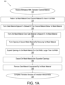
- FIG. 1A is a flow diagram illustrating methods 101 for fabricating a transistor structure having channel-symmetric gate material that is self-aligned to channel material, in accordance with some embodiments.
- Methods 101 begin at input 110 with receipt of a workpiece including transistor channel material.
- the channel material is made non-planar (e.g., into a "fin") according to a first lithographic patterning process.
- a first mask material over the channel material is patterned concurrently with the channel material to have a lateral width in a first dimension.
- gate material is formed adjacent to a sidewall of the channel material and recessed below the first mask material.
- a second mask material is formed over the gate material and adjacent to the first mask material.
- an opening is formed in the second mask material by removing the first mask material. This opening is therefore self-aligned to the underlying channel material.
- the opening is laterally expanded to a second width in the first direction, for example by recessing sidewalls of the second mask material with an etch process.
- a third mask material is deposited into the enlarged opening so that the third mask material has the second width and remains self-aligned to the underlying channel material.
- gate material unprotected by the third mask material may then be removed, for example with any suitable etch process(es) that removes the second mask material and underlying gate material.
- Methods 101 end at output 170 where the transistor structure and/or transistor interconnects (i.e., metallization lines and vias) may be completed according to any integrate circuit fabrication techniques known in the art.
- the enlarged third mask material may function as a protective cap self-aligned to the channel material so that an amount by which a gate material extends laterally beyond the channel material is ensured to be symmetrical about a centerline of the channel material. Accordingly, gate material may be more precisely controlled to have a minimal amount of overlap beyond the channel material without risk of inadvertently exposing one side of the channel material, for example because of misalignment between multiple lithographic patterning processes. With methods 101 providing minimal gate end overlap, end-to-end spacing of adjacent gate material may be maximized for a given transistor pitch, thereby achieving a reduction in parasitic capacitance.
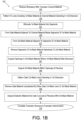
- FIG. 1B is a flow diagram illustrating methods 102 for forming a transistor structure having a channel-symmetric gate material that is self-aligned to transistor channel material, in accordance with some further embodiments.
- Methods 102 illustrate some specific implementations of methods 101 although other implementations of methods 101 are also possible. While methods 102 further illustrate many advantages of methods 101, not all aspects of methods 102 need be practiced in all implementations of methods 101.
- FIG. 2-12A are isometric views of transistor structures evolving as the methods 102 are practiced, in accordance with some embodiments. The depicted transistor structures further highlight structural features associated with an exemplary practice of methods 102. However, the practice of methods 102 need not result in all the structures exactly as illustrated in FIG. 2-12A .
- methods 102 again begin at input 110 with receipt of a workpiece including transistor channel material.
- the workpiece received at input 110 comprise a 300-450 mm diameter wafer.
- the workpiece may include a substantially monocrystalline material and any number of channel material layers over the monocrystalline material.
- the workpiece further includes a mask material over the channel material layer(s).
- a workpiece portion 201 comprises a mask material 215 over a transistor channel material stack 210 that further includes a plurality of bi-layers. Each bilayer comprising a sacrificial material 211 and a channel material 212. The number of bi-layers may vary with implementation.
- Channel material 212 may have any composition suitable for a channel of a field effect transistor (FET).
- channel material 212 is substantially silicon.
- channel material 212 comprises germanium (e.g., Si 1-x Ge X , Ge 1-x Sn X , or substantially pure Ge).
- channel material 212 includes a transition metal and a chalcogen.
- the transition metal may be any transition metal such as any element of groups 4 through 11, the group 3 elements scandium and yttrium, and the inner transition metals (e.g., f-block lanthanide and actinide series). Notable transition metals are molybdenum and tungsten.
- the chalcogen may be sulfur, selenium, and tellurium.
- channel material 212 comprises one or more metals and oxygen (i.e., metal oxide semiconductor), such as, but not limited to, Indium, gallium zinc oxide (IGZO).
- Channel material 212 is advantageously crystalline. Although the crystalline semiconductor includes polycrystalline thin film material, channel material 212 may be substantially monocrystalline. In some embodiments where channel material 212 is substantially pure silicon, the crystallinity of channel material 212 is cubic with a top surface having crystallographic orientation of (100), (111), or (110), for example. Other crystallographic orientations are also possible. Channel material 212 may also be polycrystalline or amorphous, for example in certain metal chalcogen and/or metal oxide embodiments.
- Sacrificial material 211 has a different composition than channel material 212.
- sacrificial material 211 has more germanium than channel material 212.
- sacrificial material 211 is Si 1-x Ge X , and X may be advantageously between 0.3-0.35.
- sacrificial material 211 has less germanium than channel material 212.
- the channel material 212 is Si 1-x Ge X
- sacrificial material 211 may be predominantly silicon.
- sacrificial material 211 may be a second metal chalcogenide or a metal oxide, for example.
- Mask material 215 may have any composition known to be suitable as a hardmask for patterning channel material stack 210.
- mask material 215 is a dielectric material, such as, but not limited to silicon oxide (SiO), silicon nitride (SiN), silicon oxynitride, (SiON).
- SiO silicon oxide
- SiN silicon nitride
- SiON silicon oxynitride
- FIG. 2 mask material 215 may comprise one or more material layers having a total thickness T0. Thickness T0 may vary with implementation, but in some examples is within the range of 20-60 nm.
- methods 102 continue at block 116 where fin lines are patterned into the channel material layers(s) and into any overlying mask material layer(s).
- the fin lines may extend any length along a first dimension and have a width in a second, orthogonal dimension. Any lithographic masking process and material etch process(es) may be practiced at block 116.
- lines 320 have been patterned into workpiece portion 201. Each line 320 comprises channel material stack 210 and mask material 215. Each line 320 may also comprise a sub-fin portion of underlying substrate material 205. Lines 320 are substantially parallel and extend laterally a longitudinal length in the x-dimension.
- An arrow demarks a centerline (C L ) of one line 320 that is coincident with an x-axis.
- a lithographic mask 322 defined lines 320 to have a first lateral width W1 coincident with the y-axis (i.e., orthogonal to the direction of the longitudinal centerline). Laterally adjacent fin lines 320 are separated by a space S1. Line width W1 and space S1 define an y-dimensional pitch of lines 320.
- methods 102 continue at block 121 where the line mask material is bifurcated into segments with each segment located over a transistor channel region.
- This bifurcation may be with a second lithographic patterning process defining lines that are substantially orthogonal to the fin lines.
- workpiece portion 201 now includes an isolation material 408 between fin lines 320.
- Any suitable gate mandrel material 425 is deposited over the fin lines 320 and patterned into gate mandrel lines 435 according to a photolithographically patterned mask 430. As shown, gate mandrel lines 435 are substantially parallel and extend laterally over a longitudinal length coincident with the y-axis.
- Each gate mandrel line 435 has a transverse length L1 that is over an underlying segment of mask material 215 and, below that, a length of channel material stack 210. Between adjacent gate mandrel lines 435 is a space S2. With each gate mandrel line 435 protecting underlying channel material, source and drain material (not depicted) may be formed within spaces S2 to couple with ends of each transistor channel region. Any technique(s) may be practiced to form source and drain regions, for example comprising a high concentration of impurities that impart either p-type or n-type conductivity.
- spacer materials 541 and 542 may be deposited by any process and then planarized with a top surface of mask material 215 and/or gate mandrel material 425.
- a gate spacer may have any composition, in exemplary embodiments spacer materials 541 and 542 are both dielectrics.
- spacer material 541 and/or 542 has a different chemical composition than that of mask material 215.
- Spacer material 541 and/or 542 may also have a different composition than the gate mandrel lines so that the gate mandrel lines may be removed selectively to spacer material 541 and/or 542.
- removal of the gate mandrel lines exposes mask material segments 501 of mask material 215. Below each mask material segment 501 is channel material 212. Each mask material segment 501 has the length L1 and the width W1.
- Methods 102 continue at block 126 where gate material is formed adjacent to the channel material.
- Any suitable gate material(s) may be formed over one or more surfaces of the channel material.
- gate material is formed at least adjacent to a sidewall of channel material.
- Gate material may be formed over any gate insulator suitable for the channel material composition.
- Gate material may also have any composition suitable for the channel material composition, for example to achieve a desired transistor threshold voltage, etc.
- gate material 650 is occupying a region between adjacent spacer material 541. As shown, gate material 650 backfills channel regions where sacrificial material has been removed from between layers of channel material 212. Any gate insulator material 652, such as a high-k (e.g., >9) dielectric including oxygen and silicon or one or more metals, may be between channel material 212 and gate material 650. Gate material 650 may be deposited to be essentially where the gate mandrel material was previously removed. Gate material 650 may have any composition, for example comprising platinum, nickel, molybdenum, tungsten, titanium, nitrides such as titanium nitride, or tungsten silicon nitride, or the like.
- gate material 650 includes a work function metal and a fill metal. Gate material 650 may be deposited and planarized with a surface of mask material 215 and/or spacer materials 541, 542. Following planarization, a gate material top surface 651 may be recessed with any suitable gate etch process to expose sidewalls of mask material 215.
- the gate recess etch is selective to gate material 650, ensuring mask material 215 and spacer material(s) 541, 542 are adequately retained. The recess etch of gate material 650 may expose any thickness T0' of mask material 215.
- methods 102 ( FIG. 1B ) continue with blocks 131-146 perfecting a mask polarity switch that facilitates laterally expanding the width of the mask material segments 501.
- the mask expansion retains symmetry of the mask material about the centerline of the channel region.
- a second mask material is formed laterally adjacent to the first mask material.
- This second mask material is deposited upon the underlying gate material and is then planarized with the first mask material and/or surrounding gate spacer.
- the mask material deposited at block 131 advantageously has a chemical composition distinct from the first mask material facilitating a subsequent removal of the first mask material selective of the second mask material.
- mask material 755 occupies the region from where gate material 650 was recessed.
- Mask material 755 may be deposited according to any technique and subsequently planarized with a top surface of mask material 215 and/or spacer materials 541, 542.
- mask material 755 has a second composition (e.g., comprising more carbon, more oxygen, less silicon, or less nitrogen than mask material 215).
- mask material 755 may be amorphous carbon (a-carbon).
- methods 102 continue at block 136 where the first mask material is removed. Because the second mask material has a different composition than the first mask material, the first mask material can be removed selectively to the second mask material (e.g., with any chemical etch process suitable for the composition of the first mask material). The etch performed at block 136 may also remove one or more of residual gate insulator material, residual spacer material, residual isolation material, or any other residual thin film material that may have collected at the interface between adjacent sidewalls of the first and second mask materials. Block 136 therefore completes a polarity change of the channel region mask, leaving an opening over only the channel region of a transistor with a self-aligned mask material adjacent to the opening.
- workpiece portion 201 now comprises openings 860 where mask material 215 has been etched away selectively to mask material 755.
- openings 860 have the same lateral dimensions (e.g., width W1 and length L1) that were previously defined for a mask material segment.
- Openings 860 are also similarly co-linear along a centerline (C L ) demarked by an arrow, which in the illustrated example is coincident with the x-axis.
- Openings 860 are symmetrical about the depicted centerline (C L ) of channel material 212.
- methods 102 continue at block 141 where the openings formed by removing the first mask material are laterally expanded from their initial width to some larger width by eroding the second mask material.
- This lateral expansion may comprise an etch along at least a portion of a sidewall of the opening proximal to the second mask material.
- the etch performed at block 141 may remove one or more of residual gate insulator material, residual spacer material, residual isolation material, or any other residual thin film material that may have collected as a lining on a sidewall of the first mask material prior to deposition of the second mask material.
- mask material 755 is exposed and etched either isotropically or with an angled (sloped) directional ion etch that can be controlled to recess a sidewall of mask material 755 by equal amounts on opposite sides of a centerline length L1 through opening 860 to reach a desired width W2, which is larger in the y-dimension than width W1 ( FIG. 8 ). With the increased width W2 remains centered about a centerline of opening 860 aligned with the x-dimension. Opening 860 remains self-aligned to the underlying channel material 212. As further shown in FIG. 9 , the etchback of mask material 755 is selective to spacer materials 541, 542 such that opening 860 remains of length L1.
- methods 102 continue at block 146 where another (i.e., third) mask material is deposited into the enlarged opening.
- the third mask material may again be planarized with a top surface of the surrounding materials.
- the mask material deposited at block 146 is advantageously has a different composition than the mask material deposited at block 131.
- the mask material deposited at block 146 is advantageously of a composition that will be resistant to a subsequent etch of the underlying gate material.
- the mask material deposited at block 146 may be of substantially the same composition as the mask material previously removed to form the opening within which the mask material was deposited.
- the mask material deposited at block 146 may be of a different composition than the initial mask material employed during a fin line etch.
- mask material 1060 has been deposited into the openings adjacent to mask material 755. As shown, each cap of mask material 1060 is aligned along the original fin centerline demarked by an arrow coincident with the x-axis. Each cap of mask material 1060 has a length of approximately L1 and has the width W2, which is symmetrical and/or centered about the fin centerline (C L ). Gate material 650 and channel material 212 are under mask material 1060.
- the cap With gate material protected by a cap of mask material having a self-aligned expanded width, the cap may be employed as an etch mask during a patterning process that defines a width of the gate material at block 151 ( FIG. 1B ).
- This "gate-cut" patterning process may, for example, pattern lines substantially parallel to the fin lines patterned at block 116.
- the patterning process at block 151 may entail any lithographic technique(s) and can be expected to have some non-zero misregistration relative to the patterning process performed at block 116.
- FIG. 11 illustrates workpiece portion 201 after patterning mask lines 1165.
- mask lines 1165 have a centerline (C L '), which may be approximately aligned with fin line centerline (C L ), but have some non-zero misregistration (C L -C L ').
- each mask line 1165 overlapping mask material 1060 has a width W3 that is sufficient smaller than width W2 to ensure edges of mask material 1060 extend beyond edges of mask line 1165 so that a misregistration of mask lines 1165 does not impact the patterning of gate material 650 proximal to channel material 212.
- methods 102 continue at block 155 where gate material not protected by either the mask material formed at block 146 or the mask material formed at block 151 is removed.
- the gate-cut pattern generated at block 156 is a summation of the polygons of mask material formed at block 146 and polygons defined lithographically at block 151.
- the mask pattern defined at block 151 may therefore overlap the mask material deposited at block 146, or not. Any etch process capable of removing gate material of a particular composition may be practiced at block 156.
- gate cut trenches 1170 have been etched into workpiece portion 201. As shown, trenches 1170 are located within spaces between adjacent mask lines 1165 and are further limited by the presence of mask material 1060. Trenches 1170 extend through gate material 650, exposing isolation material 408, and may extend into and/or through isolation material 408 (e.g., into substrate material 205). In this example, trenches 1170 also extend through spacer materials 541, 542. The depicted shouldering or necking of mask material 1060 is indicative of incomplete consumption of the thickness of mask material 1060 during the gate cut/trench etch process, which ensures all gate material under mask material 1060 is protected from the etch process. Hence, mask material thickness T1 may be selected to ensure mask material 1060 survives the gate cut etch process(es). The thickness T1 may then be used to determine minimum thicknesses of the preceding mask materials from which mask material 1060 is derived.
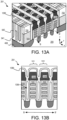
- FIG. 12B is a cross-sectional view along the B-B' line illustrated in FIG. 12A .
- two adjacent transistor structures 1201 and 1202 are laterally separated by one trench 1170.
- Gate material 650 is centered about the centerline (C L ) of channel material 212 for each transistor structure 1201, 1202. Accordingly, gate material 650 has sidewalls 1275 and 1275' on opposite sides of the channel centerline that are spaced the same distance D1 from the channel centerline.
- a lateral gate overlap width W4 beyond an adjacent sidewall of channel material is therefore equal on both sides of the channel centerline within the y-z plane illustrated in FIG. 12A .
- a centerline (CL) of trench 1170 is precisely spaced by distance D2 symmetrically between two adjacent transistor structures 1201, 1202. Accordingly, gate material end-to end spacing is equal to approximately twice distance D2, which is fin pitch in the y-dimension, minus twice distance D1.
- gate material sidewalls 1275 and 1275' may be laterally recessed, in accordance with some further embodiments.
- an etch process may be practiced to reduce the gate overlap width to W5.
- Gate material sidewalls 1275 and 1275' are then spaced the same distance D3 from the channel centerline and mask material 1060 overhangs gate material sidewalls 1275 and 1275' by a lateral distance D4 indicative of the gate material recess etch.
- any isotropic or directional ion etch process may be practiced to trim the lateral width (e.g., y-dimension) of gate material 650 to be something smaller than width W2 of mask material 1060. Accordingly, gate material end-to end spacing becomes equal to approximately twice distance D2 minus twice distance D3, which has been reduced from distance D1 by the distance D4.
- FIG. 12D illustrates a cross-sectional view again along the B-B' plane, but passing through source (drain) material 1285.
- spacer material 542 is over source (drain) material 1285.
- Trench 1170 pass through both spacer material 542 and source (drain) material 1285.
- Source (drain) material 1285 is therefore not self-aligned to a centerline (C L ) of channel material 212.
- one source (drain) material sidewall 1286 is a distance D5 from the channel material centerline while an opposing sidewall 1286' on the opposite side of the channel material centerline (within y-z plane) is a different distance D6 from the channel material centerline.
- overlap of source (drain) material is of differing widths W5 and W6. This difference may be a result of misalignment in the gate-cut mask, for example, and therefore the source (drain) cross-section in FIG. 12D serves as a useful reference to the gate cross-sections of FIG. 12A-12C .
- gate material is more symmetrical about a centerline of the channel material than source (drain) material.
- methods 102 continue at block 166 where the trenches formed at block 156 may be at least partially backfilled, and advantageously planarized with the mask material retained over the gate material. Any dielectric material may be deposited at block 166, including SiO, SiN, SiON, or low-k dielectric material, etc. Methods 102 then end at output 170 where the transistor structures and/or transistor interconnects are completed, for example according to any known techniques.
- dielectric material 1390 has been deposited over workpiece portion 201 and then planarized with surrounding mask material 1060 and spacer materials 541, 542.
- the necked or shouldered profile of each cap of mask material 1060 within the y-z plane may be advantageously levered for air-gap isolation between gate material of adjacent transistor structures.
- gate material 650 of transistor structure 1201 is separated from gate material 650 of transistor structure 1202 by an air gap, space, or void 1395 where there is no dielectric material 1390.
- Such a structure may offer lower effective transistor capacitance than for structures where dielectric material 1390 completely fills the trench between two adjacent transistor structures.
- dielectric material 1390 may occlude the voids 1395 at a pinch point between adjacent caps of mask material 1060. Occlusion may be achieved with a substantially conformal deposition process, for example.
- FIG. 14 illustrates a mobile computing platform 1405 and a server machine 1406 employing a packaged IC die including a channel-symmetric gate, for example as described elsewhere herein.
- Server machine 1406 may be any commercial server, for example including any number of high-performance computing platforms disposed within a rack and networked together for electronic data processing, which in the exemplary embodiment includes a packaged IC die comprising a fin-symmetrical gate, for example as described elsewhere herein.
- the mobile computing platform 1405 may be any portable device configured for each of electronic data display, electronic data processing, wireless electronic data transmission, or the like.
- the mobile computing platform 1405 may be any of a tablet, a smart phone, laptop computer, etc., and may include a display screen (e.g., a capacitive, inductive, resistive, or optical touchscreen), an integrated system 1410, and a battery 1415.
- a power management integrated circuit (PMIC) or RF (wireless) integrated circuit (RFIC) including a wideband RF (wireless) transmitter and/or receiver may be further coupled to IC 1400.
- PMIC power management integrated circuit
- RFIC wireless
- a PMIC may perform battery power regulation, DC-to-DC conversion, etc., and so has an input coupled to battery 1415 and an output providing a current supply to other functional modules.
- An RFIC may have an output coupled to an antenna (not shown) to implement any of a number of wireless standards or protocols, including but not limited to Wi-Fi (IEEE 802.11 family), WiMAX (IEEE 802.16 family), IEEE 802.20, long term evolution (LTE), Ev-DO, HSPA+, HSDPA+, HSUPA+, EDGE, GSM, GPRS, CDMA, TDMA, DECT, Bluetooth, derivatives thereof, as well as any other wireless protocols that are designated as 3G, 4G, 5G and beyond.
- Wi-Fi IEEE 802.11 family
- WiMAX IEEE 802.16 family
- IEEE 802.20 long term evolution (LTE), Ev-DO, HSPA+, HSDPA+, HSUPA+, EDGE, GSM, GPRS, CDMA, TDMA, DECT, Bluetooth, derivatives thereof, as well as any other wireless protocols that are designated as 3G, 4G, 5G and beyond.
- LTE long term evolution
- Ev-DO HSPA+
- FIG. 15 is a block diagram of a cryogenically cooled computing device 1500 in accordance with some embodiments.
- one or more components of computing device 1500 may include any of the channel-symmetric gate structures discussed elsewhere herein.
- a number of components are illustrated in FIG. 15 as included in computing device 1500, but any one or more of these components may be omitted or duplicated, as suitable for the application.
- some or all of the components included in computing device 1500 may be attached to one or more printed circuit boards (e.g., a motherboard).
- various ones of these components may be fabricated onto a single system-on-a-chip (SoC) die.
- SoC system-on-a-chip
- computing device 1500 may not include one or more of the components illustrated in FIG.
- computing device 1500 may include interface circuitry for coupling to the one or more components.
- computing device 1500 may not include a display device 1503, but may include display device interface circuitry (e.g., a connector and driver circuitry) to which display device 1503 may be coupled.
- display device interface circuitry e.g., a connector and driver circuitry
- Processing device 1501 may include a memory 1502, which may itself include one or more memory devices such as volatile memory (e.g., dynamic random-access memory (DRAM)), nonvolatile memory (e.g., read-only memory (ROM)), flash memory, solid state memory, and/or a hard drive.
- volatile memory e.g., dynamic random-access memory (DRAM)
- nonvolatile memory e.g., read-only memory (ROM)
- flash memory e.g., compact flash memory (SD)
- solid state memory e.g., compact flash memory (SD)
- a hard drive e.g., compact flash memory (SD)
- eDRAM embedded dynamic random-access memory
- STT-M RAM spin transfer torque magnetic random-access memory
- Communication chip 1507 may implement any of a number of wireless standards or protocols, including but not limited to Institute for Electrical and Electronic Engineers (IEEE) standards including Wi-Fi (IEEE 802.11 family), IEEE 802.16 standards (e.g., IEEE 802.16-2005 Amendment), Long-Term Evolution (LTE) project along with any amendments, updates, and/or revisions (e.g., advanced LTE project, ultramobile broadband (UMB) project (also referred to as "3GPP2”), etc.).
- IEEE 802.16 compatible Broadband Wireless Access (BWA) networks are generally referred to as WiMAX networks, an acronym that stands for Worldwide Interoperability for Microwave Access, which is a certification mark for products that pass conformity and interoperability tests for the IEEE 802.16 standards.
- communication chip 1507 may manage wired communications, such as electrical, optical, or any other suitable communication protocols (e.g., the Ethernet). As noted above, communication chip 1507 may include multiple communication chips. For instance, a first communication chip 1507 may be dedicated to shorter-range wireless communications such as Wi-Fi or Bluetooth, and a second communication chip 1507 may be dedicated to longer-range wireless communications such as GPS, EDGE, GPRS, CDMA, WiMAX, LTE, EV-DO, or others. In some embodiments, a first communication chip 1507 may be dedicated to wireless communications, and a second communication chip 1507 may be dedicated to wired communications.
- wired communications such as electrical, optical, or any other suitable communication protocols (e.g., the Ethernet).
- communication chip 1507 may include multiple communication chips. For instance, a first communication chip 1507 may be dedicated to shorter-range wireless communications such as Wi-Fi or Bluetooth, and a second communication chip 1507 may be dedicated to longer-range wireless communications such as GPS, EDGE, GPRS, CDMA, WiMAX
- Computing device 1500 may include an audio output device 1504 (or corresponding interface circuitry, as discussed above). Audio output device 1504 may include any device that generates an audible indicator, such as speakers, headsets, or earbuds, for example.
- Computing device 1500 may include a global positioning system (GPS) device 1509 (or corresponding interface circuitry, as discussed above). GPS device 1509 may be in communication with a satellite-based system and may receive a location of computing device 1500, as known in the art.
- GPS global positioning system
- Computing device 1500 may include another input device 1511 (or corresponding interface circuitry, as discussed above). Examples may include an accelerometer, a gyroscope, a compass, an image capture device, a keyboard, a cursor control device such as a mouse, a stylus, a touchpad, a bar code reader, a Quick Response (QR) code reader, any sensor, or a radio frequency identification (RFID) reader.
- an accelerometer a gyroscope, a compass
- an image capture device such as a keyboard
- a cursor control device such as a mouse, a stylus, a touchpad, a bar code reader, a Quick Response (QR) code reader, any sensor, or a radio frequency identification (RFID) reader.
- QR Quick Response
- RFID radio frequency identification
- a transistor structure comprises a channel material having a first lateral width in a first dimension and a mask material over the channel material.
- the mask material has a second lateral width in the first dimension, the second lateral width larger than the first lateral width.
- a gate material is adjacent to the channel material and under the mask material.
- the gate material has a third lateral width in the first dimension, the third lateral width smaller than the second lateral width.
- a first sidewall of the gate material is laterally offset from a first sidewall of the mask material by substantially a same distance as a second sidewall of the gate material is laterally offset from a second sidewall of the mask material.
- a centerline of the channel material is coincident with a centerline of the gate material.
- a sidewall of the gate material is recessed from a sidewall of the mask material by a distance that is symmetrical about a centerline of the first lateral width.
- the mask material has a first lateral length in a second dimension, orthogonal to the first dimension, and the gate material has a second lateral length in the second dimension.
- the second lateral length is smaller than the first lateral length.
- a difference between the first and second lateral lengths is unequal to a difference between the second and third lateral widths.
- the transistor structure comprises a source and a drain coupled at opposite ends of the channel material within a second dimension substantially orthogonal to the first dimension.
- the source and the drain each comprise an impurity-doped material epitaxial to the channel material.
- the impurity-doped material has a fourth width in the first dimension, and the fourth width is larger than the first lateral width.
- the fourth width is asymmetrical about a centerline of the first lateral width.
- the fourth width is larger than the third lateral width.
- the channel material comprises a first channel material layer in a stack with a second channel material layer, and the gate material is between the first channel material layer and the second channel material layer.
- an integrated circuit (IC) device comprises a first transistor structure comprising a first channel material having a first lateral width in a first dimension, and a first gate material laterally adjacent to the first channel material.
- the first gate material has a second lateral width in the first dimension.
- the second lateral width is substantially centered with the first lateral width of the first channel material.
- the IC device comprises a second transistor structure laterally adjacent to the first transistor structure.
- the second transistor structure comprises a second channel material having the first lateral width in the first dimension, and a second gate material laterally adjacent to the second channel material.
- the second gate material has the second lateral width in the first dimension.
- the second lateral width is substantially centered with the first lateral width of the second channel material.
- the IC device further comprises a first mask material over the first gate material.
- the first mask material comprising a dielectric.
- the IC device further comprises second mask material over the second gate material, the second mask material comprising the dielectric.
- the IC device further comprises a dielectric material layer over the first mask material, over the second mask material and within a space therebetween. The dielectric material layer occludes a space between adjacent sidewalls of the first and second gate materials.
- the space between the adjacent sidewalls of the first and second gate materials has a larger width than that of the space between the first mask material and the second mask material.
- any of the tenth through twelfth examples at least a portion of the space between the adjacent sidewalls of the first and second gate materials is unfilled by the dielectric material layer.
- the first transistor structure further comprises a first source and first drain coupled at opposite ends of the first channel material within a second dimension substantially orthogonal to the first dimension.
- the first source and the first drain comprise a first impurity-doped material epitaxial to the first channel material.
- the first impurity-doped material has a fourth lateral width in the first dimension, the fourth lateral width larger than the first lateral width.
- Th second transistor structure further comprises a second source and a second drain coupled at opposite ends of the second channel material within the second dimension.
- the second source and the second drain each comprise a second impurity-doped material epitaxial to the second channel material.
- the second impurity-doped material has the fourth lateral width in the first dimension.
- a centerline of a space between the first source and the second source or between the first drain and the second drain is off-center from a centerline the first lateral width of the first channel material and the second channel material.
- a centerline of a space between the first and second gate materials is substantially centered between a centerline the first lateral width of the first channel material and a centerline of the first lateral width of the second channel material.
- a method comprises patterning a first mask material over a transistor channel material, the first mask material of a first width in a first dimension.
- the method comprises forming a gate material adjacent to a sidewall of the transistor channel material below the first mask material.
- the method comprises forming a second mask material over the gate material and adjacent to the first mask material.
- the method comprises forming an opening in the second mask material by removing the first mask material.
- the method comprises expanding the opening to have a second width in the first dimension, larger than the first width and depositing a third mask material into the opening, the third mask material of the second width in the first dimension.
- the method comprises removing a portion of the gate material unprotected by the third mask material.
- patterning the first mask material defines first lines extending in a second direction, orthogonal to the first dimension, and removing the portion of the gate material comprises etching a trench through a portion of the second mask material and through the portion of the gate material under the portion of the second mask material.
- the method further comprises defining etch mask lines over the second and third mask materials, the etch mask lines substantially parallel to the first lines and etching the trench within a space between adjacent ones of the etch mask lines.
- removing the portion of the gate material comprises defining a gate structure having a third width in the first dimension, the third width smaller than the second width.
- the method further comprises depositing a dielectric material over the third mask material, wherein the depositing occludes a second opening formed by removing the gate material.
- the above embodiments are not limited in this regard, and, in various implementations, the above embodiments may include the undertaking of only a subset of such features, undertaking a different order of such features, undertaking a different combination of such features, and/or undertaking additional features than those features explicitly listed.
- the scope of the invention should, therefore, be determined with reference to the appended claims, along with the full scope of equivalents to which such claims are entitled.
Landscapes
- Metal-Oxide And Bipolar Metal-Oxide Semiconductor Integrated Circuits (AREA)
- Semiconductor Memories (AREA)
- Insulated Gate Type Field-Effect Transistor (AREA)
Applications Claiming Priority (1)
| Application Number | Priority Date | Filing Date | Title |
|---|---|---|---|
| US18/129,700 US20240332290A1 (en) | 2023-03-31 | 2023-03-31 | Transistor with channel-symmetric gate |
Publications (2)
| Publication Number | Publication Date |
|---|---|
| EP4439675A2 true EP4439675A2 (de) | 2024-10-02 |
| EP4439675A3 EP4439675A3 (de) | 2024-11-13 |
Family
ID=89121964
Family Applications (1)
| Application Number | Title | Priority Date | Filing Date |
|---|---|---|---|
| EP23214822.1A Pending EP4439675A3 (de) | 2023-03-31 | 2023-12-07 | Transistor mit kanalsymmetrischem gate |
Country Status (2)
| Country | Link |
|---|---|
| US (1) | US20240332290A1 (de) |
| EP (1) | EP4439675A3 (de) |
Family Cites Families (2)
| Publication number | Priority date | Publication date | Assignee | Title |
|---|---|---|---|---|
| DE102020131611B4 (de) * | 2020-05-28 | 2025-03-27 | Taiwan Semiconductor Manufacturing Co., Ltd. | Halbleitervorrichtung mit luftspalten und verfahren zu deren herstellung |
| US11450662B2 (en) * | 2020-08-10 | 2022-09-20 | Taiwan Semiconductor Manufacturing Co., Ltd. | Gate isolation structure |
-
2023
- 2023-03-31 US US18/129,700 patent/US20240332290A1/en active Pending
- 2023-12-07 EP EP23214822.1A patent/EP4439675A3/de active Pending
Also Published As
| Publication number | Publication date |
|---|---|
| EP4439675A3 (de) | 2024-11-13 |
| US20240332290A1 (en) | 2024-10-03 |
Similar Documents
| Publication | Publication Date | Title |
|---|---|---|
| US12165928B2 (en) | Integrated circuits with recessed gate electrodes | |
| KR102603279B1 (ko) | 양쪽 사이드들 상의 금속화가 있는 반도체 디바이스들에 대한 후면 콘택트 저항 감소 | |
| KR101681633B1 (ko) | 핀 기반 트랜지스터를 위한 고 이동도를 갖도록 변형된 채널을 포함하는 반도체 장치, 이동 컴퓨팅 장치, 통신장치, 이동 컴퓨팅 시스템 | |
| EP3326206B1 (de) | Herstellungsverfahren eines transistors mit luftabstandhalter | |
| TWI870463B (zh) | 具有用於子鰭部電氣接觸之相鄰結構的環繞式閘極積體電路結構 | |
| CN117616553A (zh) | 形成空腔间隔物和源极-漏极外延生长以缩小环栅晶体管 | |
| EP4439675A2 (de) | Transistor mit kanalsymmetrischem gate | |
| US20250006810A1 (en) | Transistor with channel-symmetric gate | |
| US20250113564A1 (en) | Epi height reduction for improved transistor performance | |
| US20260096142A1 (en) | Transistor source & drain contact structures comprising a laterally scaled cap | |
| US20250220944A1 (en) | Method of controlling metal gate height and selective spacer formation | |
| CN116259629A (zh) | 具有最大化沟道尺寸的集成电路结构 | |
| EP4590088A2 (de) | Hv-transistoren und widerstände für gestapelte transistorarchitekturen | |
| US20260006873A1 (en) | Fabrication of ribbon cfets with optimized nmos and pmos channel materials | |
| EP4718993A1 (de) | Hybride (100)-oberflächen und 110-oberflächen band-fets in integriertem prozessfluss | |
| US20250006737A1 (en) | Stacked cmos transistor structures with complementary channel materials | |
| EP4579725A2 (de) | Rückseitige selbstjustierte gate-vias | |
| US20260006846A1 (en) | Sacrificial ribbon for uniform workfunction and capacitance benefits | |
| US20260006833A1 (en) | Transistor metallization endcap scaling for performance optimization | |
| US20250218937A1 (en) | Directed self assembly-enabled back-side contact arrays aligned to gate electrodes | |
| US20250113516A1 (en) | Controlled recess of dummy gate to target active transistor portion | |
| CN121751751A (zh) | 用于应变优化的互补栅极切割插塞 |
Legal Events
| Date | Code | Title | Description |
|---|---|---|---|
| PUAI | Public reference made under article 153(3) epc to a published international application that has entered the european phase |
Free format text: ORIGINAL CODE: 0009012 |
|
| STAA | Information on the status of an ep patent application or granted ep patent |
Free format text: STATUS: THE APPLICATION HAS BEEN PUBLISHED |
|
| AK | Designated contracting states |
Kind code of ref document: A2 Designated state(s): AL AT BE BG CH CY CZ DE DK EE ES FI FR GB GR HR HU IE IS IT LI LT LU LV MC ME MK MT NL NO PL PT RO RS SE SI SK SM TR |
|
| PUAL | Search report despatched |
Free format text: ORIGINAL CODE: 0009013 |
|
| AK | Designated contracting states |
Kind code of ref document: A3 Designated state(s): AL AT BE BG CH CY CZ DE DK EE ES FI FR GB GR HR HU IE IS IT LI LT LU LV MC ME MK MT NL NO PL PT RO RS SE SI SK SM TR |
|
| RIC1 | Information provided on ipc code assigned before grant |
Ipc: H01L 29/06 20060101ALN20241010BHEP Ipc: H01L 29/775 20060101ALN20241010BHEP Ipc: H01L 29/66 20060101ALI20241010BHEP Ipc: H01L 27/088 20060101ALI20241010BHEP Ipc: H01L 21/8234 20060101ALI20241010BHEP Ipc: H01L 29/423 20060101AFI20241010BHEP |
|
| STAA | Information on the status of an ep patent application or granted ep patent |
Free format text: STATUS: REQUEST FOR EXAMINATION WAS MADE |
|
| 17P | Request for examination filed |
Effective date: 20250328 |