EP4435507A1 - Display panel and display apparatus - Google Patents
Display panel and display apparatus Download PDFInfo
- Publication number
- EP4435507A1 EP4435507A1 EP21827536.0A EP21827536A EP4435507A1 EP 4435507 A1 EP4435507 A1 EP 4435507A1 EP 21827536 A EP21827536 A EP 21827536A EP 4435507 A1 EP4435507 A1 EP 4435507A1
- Authority
- EP
- European Patent Office
- Prior art keywords
- area
- layer
- light
- display panel
- display
- Prior art date
- Legal status (The legal status is an assumption and is not a legal conclusion. Google has not performed a legal analysis and makes no representation as to the accuracy of the status listed.)
- Pending
Links
Images


Classifications
-
- G—PHYSICS
- G02—OPTICS
- G02F—OPTICAL DEVICES OR ARRANGEMENTS FOR THE CONTROL OF LIGHT BY MODIFICATION OF THE OPTICAL PROPERTIES OF THE MEDIA OF THE ELEMENTS INVOLVED THEREIN; NON-LINEAR OPTICS; FREQUENCY-CHANGING OF LIGHT; OPTICAL LOGIC ELEMENTS; OPTICAL ANALOGUE/DIGITAL CONVERTERS
- G02F1/00—Devices or arrangements for the control of the intensity, colour, phase, polarisation or direction of light arriving from an independent light source, e.g. switching, gating or modulating; Non-linear optics
- G02F1/01—Devices or arrangements for the control of the intensity, colour, phase, polarisation or direction of light arriving from an independent light source, e.g. switching, gating or modulating; Non-linear optics for the control of the intensity, phase, polarisation or colour
- G02F1/13—Devices or arrangements for the control of the intensity, colour, phase, polarisation or direction of light arriving from an independent light source, e.g. switching, gating or modulating; Non-linear optics for the control of the intensity, phase, polarisation or colour based on liquid crystals, e.g. single liquid crystal display cells
- G02F1/133—Constructional arrangements; Operation of liquid crystal cells; Circuit arrangements
- G02F1/1333—Constructional arrangements; Manufacturing methods
- G02F1/1337—Surface-induced orientation of the liquid crystal molecules, e.g. by alignment layers
-
- G—PHYSICS
- G02—OPTICS
- G02B—OPTICAL ELEMENTS, SYSTEMS OR APPARATUS
- G02B5/00—Optical elements other than lenses
- G02B5/20—Filters
- G02B5/28—Interference filters
- G02B5/281—Interference filters designed for the infrared light
-
- G—PHYSICS
- G02—OPTICS
- G02F—OPTICAL DEVICES OR ARRANGEMENTS FOR THE CONTROL OF LIGHT BY MODIFICATION OF THE OPTICAL PROPERTIES OF THE MEDIA OF THE ELEMENTS INVOLVED THEREIN; NON-LINEAR OPTICS; FREQUENCY-CHANGING OF LIGHT; OPTICAL LOGIC ELEMENTS; OPTICAL ANALOGUE/DIGITAL CONVERTERS
- G02F1/00—Devices or arrangements for the control of the intensity, colour, phase, polarisation or direction of light arriving from an independent light source, e.g. switching, gating or modulating; Non-linear optics
- G02F1/01—Devices or arrangements for the control of the intensity, colour, phase, polarisation or direction of light arriving from an independent light source, e.g. switching, gating or modulating; Non-linear optics for the control of the intensity, phase, polarisation or colour
- G02F1/13—Devices or arrangements for the control of the intensity, colour, phase, polarisation or direction of light arriving from an independent light source, e.g. switching, gating or modulating; Non-linear optics for the control of the intensity, phase, polarisation or colour based on liquid crystals, e.g. single liquid crystal display cells
- G02F1/133—Constructional arrangements; Operation of liquid crystal cells; Circuit arrangements
- G02F1/1333—Constructional arrangements; Manufacturing methods
-
- G—PHYSICS
- G02—OPTICS
- G02F—OPTICAL DEVICES OR ARRANGEMENTS FOR THE CONTROL OF LIGHT BY MODIFICATION OF THE OPTICAL PROPERTIES OF THE MEDIA OF THE ELEMENTS INVOLVED THEREIN; NON-LINEAR OPTICS; FREQUENCY-CHANGING OF LIGHT; OPTICAL LOGIC ELEMENTS; OPTICAL ANALOGUE/DIGITAL CONVERTERS
- G02F1/00—Devices or arrangements for the control of the intensity, colour, phase, polarisation or direction of light arriving from an independent light source, e.g. switching, gating or modulating; Non-linear optics
- G02F1/01—Devices or arrangements for the control of the intensity, colour, phase, polarisation or direction of light arriving from an independent light source, e.g. switching, gating or modulating; Non-linear optics for the control of the intensity, phase, polarisation or colour
- G02F1/13—Devices or arrangements for the control of the intensity, colour, phase, polarisation or direction of light arriving from an independent light source, e.g. switching, gating or modulating; Non-linear optics for the control of the intensity, phase, polarisation or colour based on liquid crystals, e.g. single liquid crystal display cells
- G02F1/133—Constructional arrangements; Operation of liquid crystal cells; Circuit arrangements
- G02F1/1333—Constructional arrangements; Manufacturing methods
- G02F1/133345—Insulating layers
-
- G—PHYSICS
- G02—OPTICS
- G02F—OPTICAL DEVICES OR ARRANGEMENTS FOR THE CONTROL OF LIGHT BY MODIFICATION OF THE OPTICAL PROPERTIES OF THE MEDIA OF THE ELEMENTS INVOLVED THEREIN; NON-LINEAR OPTICS; FREQUENCY-CHANGING OF LIGHT; OPTICAL LOGIC ELEMENTS; OPTICAL ANALOGUE/DIGITAL CONVERTERS
- G02F1/00—Devices or arrangements for the control of the intensity, colour, phase, polarisation or direction of light arriving from an independent light source, e.g. switching, gating or modulating; Non-linear optics
- G02F1/01—Devices or arrangements for the control of the intensity, colour, phase, polarisation or direction of light arriving from an independent light source, e.g. switching, gating or modulating; Non-linear optics for the control of the intensity, phase, polarisation or colour
- G02F1/13—Devices or arrangements for the control of the intensity, colour, phase, polarisation or direction of light arriving from an independent light source, e.g. switching, gating or modulating; Non-linear optics for the control of the intensity, phase, polarisation or colour based on liquid crystals, e.g. single liquid crystal display cells
- G02F1/133—Constructional arrangements; Operation of liquid crystal cells; Circuit arrangements
- G02F1/1333—Constructional arrangements; Manufacturing methods
- G02F1/133357—Planarisation layers
-
- G—PHYSICS
- G02—OPTICS
- G02F—OPTICAL DEVICES OR ARRANGEMENTS FOR THE CONTROL OF LIGHT BY MODIFICATION OF THE OPTICAL PROPERTIES OF THE MEDIA OF THE ELEMENTS INVOLVED THEREIN; NON-LINEAR OPTICS; FREQUENCY-CHANGING OF LIGHT; OPTICAL LOGIC ELEMENTS; OPTICAL ANALOGUE/DIGITAL CONVERTERS
- G02F1/00—Devices or arrangements for the control of the intensity, colour, phase, polarisation or direction of light arriving from an independent light source, e.g. switching, gating or modulating; Non-linear optics
- G02F1/01—Devices or arrangements for the control of the intensity, colour, phase, polarisation or direction of light arriving from an independent light source, e.g. switching, gating or modulating; Non-linear optics for the control of the intensity, phase, polarisation or colour
- G02F1/13—Devices or arrangements for the control of the intensity, colour, phase, polarisation or direction of light arriving from an independent light source, e.g. switching, gating or modulating; Non-linear optics for the control of the intensity, phase, polarisation or colour based on liquid crystals, e.g. single liquid crystal display cells
- G02F1/133—Constructional arrangements; Operation of liquid crystal cells; Circuit arrangements
- G02F1/1333—Constructional arrangements; Manufacturing methods
- G02F1/1337—Surface-induced orientation of the liquid crystal molecules, e.g. by alignment layers
- G02F1/133776—Surface-induced orientation of the liquid crystal molecules, e.g. by alignment layers having structures locally influencing the alignment, e.g. unevenness
-
- G—PHYSICS
- G02—OPTICS
- G02F—OPTICAL DEVICES OR ARRANGEMENTS FOR THE CONTROL OF LIGHT BY MODIFICATION OF THE OPTICAL PROPERTIES OF THE MEDIA OF THE ELEMENTS INVOLVED THEREIN; NON-LINEAR OPTICS; FREQUENCY-CHANGING OF LIGHT; OPTICAL LOGIC ELEMENTS; OPTICAL ANALOGUE/DIGITAL CONVERTERS
- G02F1/00—Devices or arrangements for the control of the intensity, colour, phase, polarisation or direction of light arriving from an independent light source, e.g. switching, gating or modulating; Non-linear optics
- G02F1/01—Devices or arrangements for the control of the intensity, colour, phase, polarisation or direction of light arriving from an independent light source, e.g. switching, gating or modulating; Non-linear optics for the control of the intensity, phase, polarisation or colour
- G02F1/13—Devices or arrangements for the control of the intensity, colour, phase, polarisation or direction of light arriving from an independent light source, e.g. switching, gating or modulating; Non-linear optics for the control of the intensity, phase, polarisation or colour based on liquid crystals, e.g. single liquid crystal display cells
- G02F1/133—Constructional arrangements; Operation of liquid crystal cells; Circuit arrangements
- G02F1/1333—Constructional arrangements; Manufacturing methods
- G02F1/1339—Gaskets; Spacers; Sealing of cells
-
- G—PHYSICS
- G02—OPTICS
- G02F—OPTICAL DEVICES OR ARRANGEMENTS FOR THE CONTROL OF LIGHT BY MODIFICATION OF THE OPTICAL PROPERTIES OF THE MEDIA OF THE ELEMENTS INVOLVED THEREIN; NON-LINEAR OPTICS; FREQUENCY-CHANGING OF LIGHT; OPTICAL LOGIC ELEMENTS; OPTICAL ANALOGUE/DIGITAL CONVERTERS
- G02F1/00—Devices or arrangements for the control of the intensity, colour, phase, polarisation or direction of light arriving from an independent light source, e.g. switching, gating or modulating; Non-linear optics
- G02F1/01—Devices or arrangements for the control of the intensity, colour, phase, polarisation or direction of light arriving from an independent light source, e.g. switching, gating or modulating; Non-linear optics for the control of the intensity, phase, polarisation or colour
- G02F1/13—Devices or arrangements for the control of the intensity, colour, phase, polarisation or direction of light arriving from an independent light source, e.g. switching, gating or modulating; Non-linear optics for the control of the intensity, phase, polarisation or colour based on liquid crystals, e.g. single liquid crystal display cells
- G02F1/133—Constructional arrangements; Operation of liquid crystal cells; Circuit arrangements
- G02F1/1333—Constructional arrangements; Manufacturing methods
- G02F1/1339—Gaskets; Spacers; Sealing of cells
- G02F1/13394—Gaskets; Spacers; Sealing of cells spacers regularly patterned on the cell subtrate, e.g. walls, pillars
-
- G—PHYSICS
- G02—OPTICS
- G02F—OPTICAL DEVICES OR ARRANGEMENTS FOR THE CONTROL OF LIGHT BY MODIFICATION OF THE OPTICAL PROPERTIES OF THE MEDIA OF THE ELEMENTS INVOLVED THEREIN; NON-LINEAR OPTICS; FREQUENCY-CHANGING OF LIGHT; OPTICAL LOGIC ELEMENTS; OPTICAL ANALOGUE/DIGITAL CONVERTERS
- G02F1/00—Devices or arrangements for the control of the intensity, colour, phase, polarisation or direction of light arriving from an independent light source, e.g. switching, gating or modulating; Non-linear optics
- G02F1/01—Devices or arrangements for the control of the intensity, colour, phase, polarisation or direction of light arriving from an independent light source, e.g. switching, gating or modulating; Non-linear optics for the control of the intensity, phase, polarisation or colour
- G02F1/13—Devices or arrangements for the control of the intensity, colour, phase, polarisation or direction of light arriving from an independent light source, e.g. switching, gating or modulating; Non-linear optics for the control of the intensity, phase, polarisation or colour based on liquid crystals, e.g. single liquid crystal display cells
- G02F1/133—Constructional arrangements; Operation of liquid crystal cells; Circuit arrangements
- G02F1/136—Liquid crystal cells structurally associated with a semi-conducting layer or substrate, e.g. cells forming part of an integrated circuit
- G02F1/1362—Active matrix addressed cells
-
- G—PHYSICS
- G02—OPTICS
- G02F—OPTICAL DEVICES OR ARRANGEMENTS FOR THE CONTROL OF LIGHT BY MODIFICATION OF THE OPTICAL PROPERTIES OF THE MEDIA OF THE ELEMENTS INVOLVED THEREIN; NON-LINEAR OPTICS; FREQUENCY-CHANGING OF LIGHT; OPTICAL LOGIC ELEMENTS; OPTICAL ANALOGUE/DIGITAL CONVERTERS
- G02F1/00—Devices or arrangements for the control of the intensity, colour, phase, polarisation or direction of light arriving from an independent light source, e.g. switching, gating or modulating; Non-linear optics
- G02F1/01—Devices or arrangements for the control of the intensity, colour, phase, polarisation or direction of light arriving from an independent light source, e.g. switching, gating or modulating; Non-linear optics for the control of the intensity, phase, polarisation or colour
- G02F1/13—Devices or arrangements for the control of the intensity, colour, phase, polarisation or direction of light arriving from an independent light source, e.g. switching, gating or modulating; Non-linear optics for the control of the intensity, phase, polarisation or colour based on liquid crystals, e.g. single liquid crystal display cells
- G02F1/133—Constructional arrangements; Operation of liquid crystal cells; Circuit arrangements
- G02F1/136—Liquid crystal cells structurally associated with a semi-conducting layer or substrate, e.g. cells forming part of an integrated circuit
- G02F1/1362—Active matrix addressed cells
- G02F1/136209—Light shielding layers, e.g. black matrix, incorporated in the active matrix substrate, e.g. structurally associated with the switching element
-
- G—PHYSICS
- G02—OPTICS
- G02F—OPTICAL DEVICES OR ARRANGEMENTS FOR THE CONTROL OF LIGHT BY MODIFICATION OF THE OPTICAL PROPERTIES OF THE MEDIA OF THE ELEMENTS INVOLVED THEREIN; NON-LINEAR OPTICS; FREQUENCY-CHANGING OF LIGHT; OPTICAL LOGIC ELEMENTS; OPTICAL ANALOGUE/DIGITAL CONVERTERS
- G02F1/00—Devices or arrangements for the control of the intensity, colour, phase, polarisation or direction of light arriving from an independent light source, e.g. switching, gating or modulating; Non-linear optics
- G02F1/01—Devices or arrangements for the control of the intensity, colour, phase, polarisation or direction of light arriving from an independent light source, e.g. switching, gating or modulating; Non-linear optics for the control of the intensity, phase, polarisation or colour
- G02F1/13—Devices or arrangements for the control of the intensity, colour, phase, polarisation or direction of light arriving from an independent light source, e.g. switching, gating or modulating; Non-linear optics for the control of the intensity, phase, polarisation or colour based on liquid crystals, e.g. single liquid crystal display cells
- G02F1/133—Constructional arrangements; Operation of liquid crystal cells; Circuit arrangements
- G02F1/136—Liquid crystal cells structurally associated with a semi-conducting layer or substrate, e.g. cells forming part of an integrated circuit
- G02F1/1362—Active matrix addressed cells
- G02F1/136286—Wiring, e.g. gate line, drain line
-
- G—PHYSICS
- G03—PHOTOGRAPHY; CINEMATOGRAPHY; ANALOGOUS TECHNIQUES USING WAVES OTHER THAN OPTICAL WAVES; ELECTROGRAPHY; HOLOGRAPHY
- G03B—APPARATUS OR ARRANGEMENTS FOR TAKING PHOTOGRAPHS OR FOR PROJECTING OR VIEWING THEM; APPARATUS OR ARRANGEMENTS EMPLOYING ANALOGOUS TECHNIQUES USING WAVES OTHER THAN OPTICAL WAVES; ACCESSORIES THEREFOR
- G03B21/00—Projectors or projection-type viewers; Accessories therefor
-
- G—PHYSICS
- G03—PHOTOGRAPHY; CINEMATOGRAPHY; ANALOGOUS TECHNIQUES USING WAVES OTHER THAN OPTICAL WAVES; ELECTROGRAPHY; HOLOGRAPHY
- G03B—APPARATUS OR ARRANGEMENTS FOR TAKING PHOTOGRAPHS OR FOR PROJECTING OR VIEWING THEM; APPARATUS OR ARRANGEMENTS EMPLOYING ANALOGOUS TECHNIQUES USING WAVES OTHER THAN OPTICAL WAVES; ACCESSORIES THEREFOR
- G03B30/00—Camera modules comprising integrated lens units and imaging units, specially adapted for being embedded in other devices, e.g. mobile phones or vehicles
-
- H—ELECTRICITY
- H04—ELECTRIC COMMUNICATION TECHNIQUE
- H04M—TELEPHONIC COMMUNICATION
- H04M1/00—Substation equipment, e.g. for use by subscribers
- H04M1/02—Constructional features of telephone sets
- H04M1/0202—Portable telephone sets, e.g. cordless phones, mobile phones or bar type handsets
- H04M1/026—Details of the structure or mounting of specific components
- H04M1/0266—Details of the structure or mounting of specific components for a display module assembly
-
- G—PHYSICS
- G02—OPTICS
- G02B—OPTICAL ELEMENTS, SYSTEMS OR APPARATUS
- G02B5/00—Optical elements other than lenses
- G02B5/20—Filters
- G02B5/208—Filters for use with infrared or ultraviolet radiation, e.g. for separating visible light from infrared and/or ultraviolet radiation
-
- G—PHYSICS
- G02—OPTICS
- G02F—OPTICAL DEVICES OR ARRANGEMENTS FOR THE CONTROL OF LIGHT BY MODIFICATION OF THE OPTICAL PROPERTIES OF THE MEDIA OF THE ELEMENTS INVOLVED THEREIN; NON-LINEAR OPTICS; FREQUENCY-CHANGING OF LIGHT; OPTICAL LOGIC ELEMENTS; OPTICAL ANALOGUE/DIGITAL CONVERTERS
- G02F1/00—Devices or arrangements for the control of the intensity, colour, phase, polarisation or direction of light arriving from an independent light source, e.g. switching, gating or modulating; Non-linear optics
- G02F1/01—Devices or arrangements for the control of the intensity, colour, phase, polarisation or direction of light arriving from an independent light source, e.g. switching, gating or modulating; Non-linear optics for the control of the intensity, phase, polarisation or colour
- G02F1/13—Devices or arrangements for the control of the intensity, colour, phase, polarisation or direction of light arriving from an independent light source, e.g. switching, gating or modulating; Non-linear optics for the control of the intensity, phase, polarisation or colour based on liquid crystals, e.g. single liquid crystal display cells
- G02F1/133—Constructional arrangements; Operation of liquid crystal cells; Circuit arrangements
- G02F1/1333—Constructional arrangements; Manufacturing methods
- G02F1/1335—Structural association of cells with optical devices, e.g. polarisers or reflectors
-
- G—PHYSICS
- G02—OPTICS
- G02F—OPTICAL DEVICES OR ARRANGEMENTS FOR THE CONTROL OF LIGHT BY MODIFICATION OF THE OPTICAL PROPERTIES OF THE MEDIA OF THE ELEMENTS INVOLVED THEREIN; NON-LINEAR OPTICS; FREQUENCY-CHANGING OF LIGHT; OPTICAL LOGIC ELEMENTS; OPTICAL ANALOGUE/DIGITAL CONVERTERS
- G02F1/00—Devices or arrangements for the control of the intensity, colour, phase, polarisation or direction of light arriving from an independent light source, e.g. switching, gating or modulating; Non-linear optics
- G02F1/01—Devices or arrangements for the control of the intensity, colour, phase, polarisation or direction of light arriving from an independent light source, e.g. switching, gating or modulating; Non-linear optics for the control of the intensity, phase, polarisation or colour
- G02F1/13—Devices or arrangements for the control of the intensity, colour, phase, polarisation or direction of light arriving from an independent light source, e.g. switching, gating or modulating; Non-linear optics for the control of the intensity, phase, polarisation or colour based on liquid crystals, e.g. single liquid crystal display cells
- G02F1/133—Constructional arrangements; Operation of liquid crystal cells; Circuit arrangements
- G02F1/1333—Constructional arrangements; Manufacturing methods
- G02F1/1335—Structural association of cells with optical devices, e.g. polarisers or reflectors
- G02F1/133509—Filters, e.g. light shielding masks
- G02F1/133512—Light shielding layers, e.g. black matrix
-
- G—PHYSICS
- G02—OPTICS
- G02F—OPTICAL DEVICES OR ARRANGEMENTS FOR THE CONTROL OF LIGHT BY MODIFICATION OF THE OPTICAL PROPERTIES OF THE MEDIA OF THE ELEMENTS INVOLVED THEREIN; NON-LINEAR OPTICS; FREQUENCY-CHANGING OF LIGHT; OPTICAL LOGIC ELEMENTS; OPTICAL ANALOGUE/DIGITAL CONVERTERS
- G02F1/00—Devices or arrangements for the control of the intensity, colour, phase, polarisation or direction of light arriving from an independent light source, e.g. switching, gating or modulating; Non-linear optics
- G02F1/01—Devices or arrangements for the control of the intensity, colour, phase, polarisation or direction of light arriving from an independent light source, e.g. switching, gating or modulating; Non-linear optics for the control of the intensity, phase, polarisation or colour
- G02F1/13—Devices or arrangements for the control of the intensity, colour, phase, polarisation or direction of light arriving from an independent light source, e.g. switching, gating or modulating; Non-linear optics for the control of the intensity, phase, polarisation or colour based on liquid crystals, e.g. single liquid crystal display cells
- G02F1/133—Constructional arrangements; Operation of liquid crystal cells; Circuit arrangements
- G02F1/1333—Constructional arrangements; Manufacturing methods
- G02F1/1335—Structural association of cells with optical devices, e.g. polarisers or reflectors
- G02F1/133509—Filters, e.g. light shielding masks
- G02F1/133514—Colour filters
-
- G—PHYSICS
- G02—OPTICS
- G02F—OPTICAL DEVICES OR ARRANGEMENTS FOR THE CONTROL OF LIGHT BY MODIFICATION OF THE OPTICAL PROPERTIES OF THE MEDIA OF THE ELEMENTS INVOLVED THEREIN; NON-LINEAR OPTICS; FREQUENCY-CHANGING OF LIGHT; OPTICAL LOGIC ELEMENTS; OPTICAL ANALOGUE/DIGITAL CONVERTERS
- G02F2201/00—Constructional arrangements not provided for in groups G02F1/00 - G02F7/00
- G02F2201/40—Arrangements for improving the aperture ratio
-
- G—PHYSICS
- G02—OPTICS
- G02F—OPTICAL DEVICES OR ARRANGEMENTS FOR THE CONTROL OF LIGHT BY MODIFICATION OF THE OPTICAL PROPERTIES OF THE MEDIA OF THE ELEMENTS INVOLVED THEREIN; NON-LINEAR OPTICS; FREQUENCY-CHANGING OF LIGHT; OPTICAL LOGIC ELEMENTS; OPTICAL ANALOGUE/DIGITAL CONVERTERS
- G02F2201/00—Constructional arrangements not provided for in groups G02F1/00 - G02F7/00
- G02F2201/58—Arrangements comprising a monitoring photodetector
-
- G—PHYSICS
- G02—OPTICS
- G02F—OPTICAL DEVICES OR ARRANGEMENTS FOR THE CONTROL OF LIGHT BY MODIFICATION OF THE OPTICAL PROPERTIES OF THE MEDIA OF THE ELEMENTS INVOLVED THEREIN; NON-LINEAR OPTICS; FREQUENCY-CHANGING OF LIGHT; OPTICAL LOGIC ELEMENTS; OPTICAL ANALOGUE/DIGITAL CONVERTERS
- G02F2203/00—Function characteristic
- G02F2203/11—Function characteristic involving infrared radiation
-
- H—ELECTRICITY
- H04—ELECTRIC COMMUNICATION TECHNIQUE
- H04M—TELEPHONIC COMMUNICATION
- H04M1/00—Substation equipment, e.g. for use by subscribers
- H04M1/02—Constructional features of telephone sets
- H04M1/0202—Portable telephone sets, e.g. cordless phones, mobile phones or bar type handsets
- H04M1/026—Details of the structure or mounting of specific components
- H04M1/0264—Details of the structure or mounting of specific components for a camera module assembly
Definitions
- the present application relates to a display field, and more particularly to a display panel and a display device.
- the Liquid Crystal Display (LCD) possesses advantages of high image quality, power saving, thin body and wide application range, stable performance and safety, etc. Thus, it has been widely applied in various consumer electrical products, such as vehicles, mobile phone, television, personal digital assistant, digital camera, notebook, laptop, and becomes the major display device.
- the Driver Monitor System can monitor the driver's fatigue and improve driving safety.
- DMS Driver Monitor System
- the optical element is a camera for an illustration.
- the existing LCDs equipped with DMS function mostly adopt the solution of hiding the camera on the back of the LCD panel.
- the present application provides a display panel and a display device thereof, which can increase the light transmittance of the display panel, and reduce the difficulty for optical elements to collect external ambient light, and increase the amount of light collected by the optical element.
- the embodiment of the present application provides a display panel, wherein the display panel comprises: a first substrate and a second substrate, which are oppositely arranged, and a liquid crystal layer arranged between the first substrate and second substrate, and the first substrate and the second substrate are both provided with an alignment layer on a side close to the liquid crystal layer, wherein the display panel comprises a display area and a light-transmitting area, and at least one of the alignment layers is provided with a hole in the light-transmitting area.
- any one of the alignment layers is provided with a hole in the light-transmitting area.
- the hole is filled with an optical film material, and an infrared light transmittance of the optical film material is greater than an infrared light transmittance of the alignment layer.
- a visible light reflectivity of the optical film material is less than a visible light reflectivity of the alignment layer.
- the alignment layers comprise a first alignment layer provided on the first substrate and a second alignment layer provided on the second substrate, and the first alignment layer is provided with a first hole in the light-transmitting area and the second alignment layer is provided with a second hole in the light-transmitting area, and an area of the first hole and an area of the second hole are the same or different.
- the display area and the light-transmitting area are spaced apart, and the display panel further comprises a transition area, and the transition area is located in a gap area between the display area and the light-transmitting area, and a display panel film structure of the transition area is different from a display panel film structure of the display area and a display panel film structure of the light-transmitting area.
- the first substrate comprises: a first base substrate and a black matrix layer provided on the first base substrate, and the black matrix layer is located in the display area, and the black matrix layer comprises a black matrix ring located at a boundary of the display area and the transition area.
- the first substrate further comprises a color filter layer and a first planarization layer sequentially stacked on the black matrix layer, and the color filter layer is located in the display area, the transition area and the light transmission area, and the first planarization layer is located in the display area, the transition area and the light transmission area, and a thickness of the first planarization layer in the light-transmitting area is greater than a thickness of the first planarization layer in the display area.
- the first substrate further comprises the first alignment layer disposed on the first planarization layer, and the first alignment layer is located in the display area and the transition area, and the first alignment layer is provided with the first hole in the light-transmitting area, and an edge of the first hole is located at the boundary of the light-transmitting area and the transition area.
- the first substrate further comprises a first optical film material filled in the first hole, and an infrared light transmittance of the first optical film material is greater than an infrared light transmittance of the alignment layer.
- the first substrate further comprises a support column layer disposed between the first alignment layer and the first planarization layer, and the support column layer comprises a plurality of support columns arranged at intervals, and the plurality of support columns are located in the display area.
- the second substrate comprises: a second base substrate and a thin film transistor layer disposed on the second base substrate, and the thin film transistor layer comprises a thin film transistor and a metal trace, and the thin film transistor is located in the display area and the transition area; the metal trace is located in the display area and the transition area; wherein the metal trace located in the transition area is a ring trace.
- the thin film transistor layer further comprises an interlayer dielectric layer disposed on the second base substrate, and the interlayer dielectric layer is located in the display area and the transition area.
- the second substrate further comprises a second planarization layer disposed on the interlayer dielectric layer, and the second planarization layer is located in the display area, the transition area and the light-transmitting area, and a thickness of the second planarization layer in the light-transmitting area is greater than a thickness of the second planarization layer in the display area.
- the second substrate further comprises a composite film layer disposed on the second planarization layer, and the composite film layer comprises a first transparent conductive layer, a passivation layer and a second transparent conductive layer sequentially stacked on the second planarization layer, and the composite film layer is located in the display area.
- the second substrate further comprises a third planarization layer disposed on the composite film layer, and the third planarization layer is located in the display area, the transition area and the light-transmitting area, and a thickness of the third planarization layer in the light-transmitting area is greater than a thickness of the third planarization layer in the display area.
- the second substrate further comprises the second alignment layer disposed on the third planarization layer, and the second alignment layer is located in the display area, the transition area, and the light-transmitting area, and the second alignment layer is provided with the second hole in the light-transmitting area, and an edge of the second hole is located in the light-transmitting area.
- the second substrate further comprises a second optical film material filled in the second hole, and an infrared light transmittance of the second optical film material is greater than an infrared light transmittance of the alignment layer.
- the embodiment of the present application further provides a display device, wherein the display device comprises: an optical element, a backlight module and the display panel of any one of the above, and the backlight module is arranged on a side of the display panel, and the backlight module is provided with a light-transmitting hole at a position corresponding to the light-transmitting area; the optical element is arranged on a side of the backlight module away from the display panel, and the optical element is arranged corresponding to the light-transmitting hole.
- the optical element is an infrared camera.
- the display panel and the display device provided by the present application provide a hole in at least one alignment layer of the display panel. Therefore, when external light enters the optical element through the display panel, the filtering effect of the alignment layer on the light is greatly reduced, and light loss is reduced, to improve the light transmittance of the area of the display panel corresponding to the optical element. It is to reduce the difficulty for optical elements to collect external ambient light, and increase the amount of light collected by the optical element for improving the imaging result of the optical element.
- orientation words used such as “upper” and “lower” usually refer to the upper and lower of the device in actual use or working state, which specifically are the directions of the drawing in the figures; and “inner” and “outer” refer to the outline of the device.
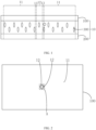
- FIG. 1 shows a structural diagram of a display panel provided by an embodiment of the present application.
- the embodiment of the present application provides a display panel 10.
- the display panel 10 comprises: a first substrate 100 and a second substrate 200.
- the first substrate 100 and the second substrate 200 are oppositely arranged.
- the display panel 10 further comprises a liquid crystal layer 300 arranged between the first substrate 100 and second substrate 200. Liquid crystal molecules are distributed in the liquid crystal layer 300, and the liquid crystal molecules can be twisted under the action of a driving electric field.
- the first substrate 100 and the second substrate 200 are both provided with an alignment layer on a side close to the liquid crystal layer 300.
- the alignment layer can provide uniformly arranged interface conditions for the liquid crystal molecules, so that the liquid crystal molecules are arranged in a predetermined order.
- FIG. 2 shows a top-view diagram of a display panel provided by an embodiment of the present application.
- the display panel 10 comprises: a display area 11 and a light-transmitting area 12.
- the display area 11 of the display panel 10 is provided with pixel units and is employed to perform display functions;
- the light-transmitting area 12 of the display panel 10 possesses the function of transmitting light, that is, the light transmittance of the light-transmitting area 12 is higher than the light transmittance of the display area 11.
- the light when an optical element is disposed on a side of the display panel 10 corresponding to a position of the light-transmitting area 12, the light can smoothly pass through the light-transmitting area 12 of the display panel 10 and can be incident on the optical element, so that the optical element normally performs a photosensitive function.
- the alignment layer on the first substrate 100 is a first alignment layer
- the alignment layer on the second substrate 200 is a second alignment layer.
- the first alignment layer and/or the second alignment layer are provided with holes (not shown in the figure) in the light-transmitting area 12. Since at least one of the alignment layers is provided with a hole in the light-transmitting area 12, the filtering effect of the alignment layer on the light penetrating the light-transmitting area 12 of the display panel 10 can be effectively reduced, and light loss is reduced, to improve the light transmittance of the display panel 10 in the light-transmitting area 12.
- the first alignment layer and the second alignment layer are both provided with holes in the light-transmitting area 12, and the hole in the first alignment layer is corresponding to the hole in the second alignment layer.
- the light transmittance of the display panel 10 in the light-transmitting area 12 can be further improved.
- the light is 940 ( ⁇ 10)nm infrared light (Infrared, IR) for instance, and the light transmittance is infrared light transmittance for instance, and the optical element possesses an infrared light sensing function for instance. Since the human body can emit infrared light, when the optical element located on the side of the display panel 10 and corresponding to the light-transmitting area 12 collects the infrared light and forms an image, it can well protect user privacy while accomplishing the monitoring requirements of DMS.
- IR infrared light
- the hole is filled with an optical film material, and a light transmittance of the optical film material is greater than a light transmittance of the alignment layer.
- a visible light reflectivity of the optical film material is less than a visible light reflectivity of the alignment layer. Since the visible light reflectivity of the optical film material is less than the visible light reflectivity of the alignment layer, the uniform display effect of the display panel 10 can be improved, and the display quality can be improved.
- the optical film material is, for instance, an antireflective film, and the antireflective film is filled in the hole of the alignment layer.
- the antireflective film can reduce the reflectivity of visible light in the display panel 10 and increase the transmittance of infrared light in the display panel 10.
- the display area 11 and the light-transmitting area 12 are spaced apart, and the display panel 10 further comprises a transition area 13, and the transition area 13 is located in a gap area between the display area 11 and the light-transmitting area 12, and a display panel film structure of the transition area 13 is different from a display panel film structure of the display area 11 and a display panel film structure of the light-transmitting area 12, and the alignment layer is at least disposed in the transition area 13 of the display panel 10.
- the gap area between the display area 11 and the light-transmitting area 12 is also provided with an alignment layer, the liquid crystal molecules located near the boundary area of the display area 11 and the transition area 13 can have the same alignment form as the liquid crystal molecules located in the display area 11 to ensure the display effect of the display area 11.
- the transition area 13 surrounds the light-transmitting area 12, and the display area 11 surrounds the transition area 13.
- the display panel 10 further comprises, for instance, a non-display area, and the non-display area is adjacent to the display area 11, and the non-display area is arranged around the display area 11.
- FIG. 3 shows a structural diagram of a first substrate in the display panel provided in the first embodiment of the present application
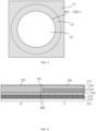
- FIG. 4 shows a diagram of a position of a black matrix ring provided in the first embodiment of the present application in the area A in FIG. 2
- FIG. 5 shows a diagram of a position of a first hole and a second hole provided in the first embodiment of the present application in the area A in FIG. 2
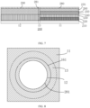
- FIG. 6 shows a structural diagram of a second substrate in the display panel provided in the first embodiment of the present application.
- the specific film structure of the first substrate 100 and the second substrate 200 in the display panel 10 will be described in detail below with reference to FIGS. 3 to 6 .
- the alignment layers comprise a first alignment layer 160 provided on the first substrate 100 and a second alignment layer 280 provided on the second substrate 200, and the first alignment layer 160 is provided with a first hole 161 in the light-transmitting area 12 and the second alignment layer 280 is provided with a second hole 281 in the light-transmitting area 12, and an area of the first hole 161 and an area of the second hole 281 are the same.
- the first substrate 100 comprises: a first base substrate 110.
- the first base substrate 110 is a carrier of other film structures on the first substrate 100, which can be a rigid substrate or a flexible substrate, and its material can be glass, plastic, or other inorganic or organic materials with excellent light transmittance.
- the first base substrate 110 is a rigid glass substrate.
- the first substrate 100 further comprises a black matrix layer 120 provided on the first base substrate 110, and the black matrix layer 120 is located in the display area 11. That is, the black matrix layer 120 is not provided in the light-transmitting area 12. Since the light-transmitting area 12 omits the black matrix layer 120 with low light transmittance, the light transmittance of the display panel 10 can be further improved.
- the black matrix layer 120 located in the display area 11 is formed with a grid-shaped black matrix structure 121.
- the infrared light transmittance of the black matrix structure 121 is 0%.
- the black matrix layer 121 comprises a black matrix ring 1211 located at a boundary of the display area 11 and the transition area 13. That is, the black matrix ring 1211 is the boundary line of the display area 11 and the transition area 13.
- the first substrate 100 further comprises a color filter layer 130 and a first planarization layer 140 sequentially stacked on the black matrix layer 120, and the color filter layer 130 is located in the display area 11, the transition area 13 and the light transmission area 12, and the first planarization layer 140 is located in the display area 11, the transition area 13 and the light transmission area 12, and a thickness of the first planarization layer 140 in the light-transmitting area 12 is greater than a thickness of the first planarization layer 140 in the display area 11.
- the color filter layer 130 located in the display area 11, the transition area 13 and the light-transmitting area 12 is formed by the same process, and the color filter layer 130 of the display area 11 comprises color resist units of multiple colors, and the color resist units are used to realize a color display function;
- the first planarization layer 140 located in the display area 11, the transition area 13 and the light-transmitting area 12 is formed by the same process, and the surface of the first planarization layer 140 away from the first base substrate 110 is a planar surface for achieving a planarizing function.
- the infrared light transmittance of the color filter layer 130 is 98%, and the infrared light transmittance of the first planarization layer 140 is 100%. Since the infrared light transmittance of the color filter layer 130 and the first planarization layer 140 are both relatively high, both the color filter layer 130 and the first planarization layer 140 remain in the display area 11 and the light-transmitting area 12.
- the first substrate 100 further comprises a first alignment layer 160 disposed on the first planarization layer 140, and the first alignment layer 160 is located in the display area 11 and the transition area 13, and the first alignment layer 160 is provided with the first hole 161 in the light-transmitting area 12, and an edge of the first hole 161 is located at the boundary of the light-transmitting area 12 and the transition area 13. That is, the edge of the first hole 161 formed in the first alignment layer 160 is the boundary line of the transition area 13 and the light-transmitting area 12.
- the infrared light transmittance of the first alignment layer 160 is 92%. Since the first alignment layer 160 is omitted in the light-transmitting area 12, the infrared light transmittance of the light-transmitting area 12 can be greatly improved.
- the first substrate 100 further comprises a first optical film material 170 filled in the first hole 161, and an infrared light transmittance of the first optical film material 170 is greater than an infrared light transmittance of the alignment layer 160. Since the first substrate 100 is formed with the first optical film material 170 with higher light transmittance in the area corresponding to the light-transmitting area 12, the infrared light transmittance of the display panel 10 in the light-transmitting area 12 can be effectively improved.
- a visible light reflectivity of the first optical film material 170 is less than a visible light reflectivity of the first alignment layer 160.
- the first optical film material 170 is, for instance, an antireflective film, and the antireflective film is filled in the first hole 161 of the alignment layer 160.
- the antireflective film can reduce the reflectivity of visible light in the display panel 10 and increase the transmittance of infrared light in the display panel 10.
- the first substrate 100 further comprises a support column layer 150 disposed between the first alignment layer 160 and the first planarization layer 140, and the support column layer 150 comprises a plurality of support columns arranged at intervals.
- the support columns can form a stable separation distance between the first substrate 100 and the second substrate 200 to ensure the normal display of the display panel 10.
- the plurality of support columns is located in the display area 11. That is, the support columns are not arranged in the light-transmitting area 12. Since the support column will diffract the infrared light, which will affect the imaging result of the optical element located on the side of the display panel, the support column is not provided in the light-transmitting area 12 in the present application. Therefore, the infrared light transmittance of the display panel 10 in the light-transmitting area 12 can be further improved, while the diffraction phenomenon can be avoided, and the imaging result of the optical element can be improved.
- the second substrate 200 comprises: a second base substrate 210 and a thin film transistor layer disposed on the second base substrate 210, and the thin film transistor layer comprises a thin film transistor and a metal trace, and the thin film transistor is located in the display area 11 and the transition area 13; the metal trace is located in the display area 11 and the transition area 13. That is, the light-transmitting area 12 is not provided with the thin film transistor and the metal trace.
- the thin film transistor and the metal trace generally comprise opaque metal material. Since the light-transmitting area 12 is not provided with the thin film transistor and the metal trace, the infrared light transmittance of the display panel 10 in the light-transmitting area 12 can be further improved.
- the thin film transistor is, for instance, low temperature polysilicon thin film transistor.
- the thin film transistor comprises various film layers.
- the various film layers comprise, for instance, a light-shielding layer, a buffer layer, a first metal layer, a gate insulating layer, an active layer, an interlayer dielectric layer 220 and a second metal layer that are sequentially stacked on the second base substrate 210.
- the light-shielding layer comprises a light-shielding pattern corresponding to a channel region of the active layer, and the light-shielding layer is located in the display area 11 and the transition area 13;
- the buffer layer is a laminated structure formed by a silicon nitride film layer and a silicon oxide film layer, and the buffer layer is located in the display area 11, the transition area 13 and the light-transmitting area 12;
- the first metal layer comprises a gate and metal trace, and the first metal layer is located in the display area 11 and the transition area 13;
- the gate insulating layer is a silicon oxide film layer, and the gate insulating layer is located in the display area 11, the transition area 13 and the light-transmitting area 12;
- the active layer comprises a channel region, a heavily doped region and a lightly doped region, and the active layer is located in the display area 11 and the transition area 13;
- the interlayer dielectric layer 220 is a laminated structure formed by a silicon nitride film layer
- the second substrate 200 further comprises a second planarization layer 230 disposed on the interlayer dielectric layer 220, and the second planarization layer 230 is located in the display area 11, the transition area 13 and the light-transmitting area 12.
- the second planarization layer 230 located in the display area 11, the transition area 13 and the light-transmitting area 12 is formed by the same process, and the surface of the second planarization layer 230 away from the second base substrate 210 is a planar surface for achieving a planarizing function.
- the second substrate 200 further comprises a composite film layer disposed on the second planarization layer 230, and the composite film layer comprises a first transparent conductive layer 240, a passivation layer 250 and a second transparent conductive layer 260 sequentially stacked on the second planarization layer 230, and the composite film layer is located in the display area 11. That is, the light-transmitting area 12 is not provided with the composite film layer, so that the infrared light transmittance of the display panel 10 in the light-transmitting area 12 can be further improved.
- the material for forming the first transparent conductive layer 240 and the second transparent conductive layer 260 is indium tin oxide (ITO), and the material for forming the passivation layer 250 is silicon nitride.
- the infrared light transmittance of the composite film layer is 72%. Since the composite film layer is not provided in the light-transmitting area 12, the infrared light transmittance of the display panel 10 in the light-transmitting area 12 can be significantly improved.
- the second substrate 200 further comprises a third planarization layer 270 disposed on the composite film layer, and the third planarization layer 270 is located in the display area 11, the transition area 13 and the light-transmitting area 12, and a thickness of the third planarization layer 270 in the light-transmitting area 12 is greater than a thickness of the third planarization layer 270 in the display area 11.
- the third planarization layer 270 located in the display area 11, the transition area 13 and the light-transmitting area 12 is formed by the same process, and the surface of the third planarization layer 270 away from the second base substrate 210 is a planar surface for achieving a planarizing function.
- the second substrate 200 further comprises the second alignment layer 280 disposed on the third planarization layer 270, and the second alignment layer 280 is located in the display area 11 and the transition area 13, and the second alignment layer 280 is provided with the second hole 281 in the boundary area of the light-transmitting area 12 and the transition area 13. That is, the edge of the second hole 281 formed in the second alignment layer 280 is the boundary line of the transition area 13 and the light-transmitting area 12.
- the second alignment layer 280 is provided with the second hole 281 in the light-transmitting area 12, and an edge of the second hole 281 is located at the boundary of the light-transmitting area 12 and the transition area 13.
- the edge of the second hole 281 formed in the second alignment layer 280 is the boundary line of the transition area 13 and the light-transmitting area 12, and an area of the second hole 281 is equal to an area of the first hole 161.
- the infrared light transmittance of the second alignment layer 280 is 92%. Since the second alignment layer 280 is omitted in the light-transmitting area 12, the infrared light transmittance of the light-transmitting area 12 can be greatly improved.
- the second substrate 200 further comprises a second optical film material 290 filled in the second hole 281, and an infrared light transmittance of the second optical film material 290 is greater than an infrared light transmittance of the alignment layer 280. Since the second substrate 200 is formed with the second optical film material 290 with higher light transmittance in the area corresponding to the light-transmitting area 12, the infrared light transmittance of the display panel 10 in the light-transmitting area 12 can be effectively improved.
- a visible light reflectivity of the second optical film material 290 is less than a visible light reflectivity of the second alignment layer 280.
- the second optical film material 290 is, for instance, an antireflective film, and the antireflective film is filled in the second hole 281 of the second alignment layer 280.
- the antireflective film can reduce the reflectivity of visible light in the display panel 10 and increase the transmittance of infrared light in the display panel 10.
- FIG. 7 shows a structural diagram of a second substrate in the display panel provided in the second embodiment of the present application.
- the second embodiment of the present application provides a display panel 10.
- the structure of the display panel 10 is similar to that of the display panel 10 in the first embodiment of the present application, and the same parts will not be repeated in this embodiment.
- the interlayer dielectric layer 220 is located in the display area 11 and the transition area 13, that is, the interlayer dielectric layer 220 is not located in the light-transmitting area 12. Therefore, the film structure of the light-transmitting area 12 is simplified, and the number of film layers is reduced, and the infrared light transmittance of the display panel 10 in the light-transmitting area 12 can be further improved.
- the second substrate 200 further comprises a second planarization layer 230 disposed on the interlayer dielectric layer 220, and the second planarization layer 230 is located in the display area 11, the transition area 13 and the light-transmitting area 12, and a thickness of the second planarization layer 230 in the light-transmitting area 12 is greater than a thickness of the second planarization layer 230 in the display area 11.
- the second planarization layer 230 located in the display area 11, the transition area 13 and the light-transmitting area 12 is formed by the same process, and the surface of the second planarization layer 230 away from the second base substrate 210 is a planar surface for achieving a planarizing function.
- FIG. 8 shows a diagram of a position of a first hole and a second hole provided in the third embodiment of the present application in the area A in FIG. 2 ;
- FIG. 9 shows a structural diagram of a second substrate in the display panel provided in the third embodiment of the present application.
- the third embodiment of the present application provides a display panel 10.
- the display panel 10 is similar in structure to the display panel 10 in the first embodiment of the present application.
- the structure of the first substrate 100 in the third embodiment is the same as that of the first substrate 100 in the first embodiment, and the same parts will not be repeated in this embodiment.
- the difference is that in the display panel 10 provided by the third embodiment of the present application, an area of the first hole 161 and an area of the second hole 281 are different.
- the first alignment layer 160 on the first substrate 100 is located in the display area 11 and the transition area 13, and the first alignment layer 160 is provided with the first hole 161 in the light-transmitting area 12, and an edge of the first hole 161 is located at the boundary of the light-transmitting area 12 and the transition area 13. That is, the edge of the first hole 161 formed in the first alignment layer 160 is the boundary line of the transition area 13 and the light-transmitting area 12; the second alignment layer 280 on the second substrate 200 is located in the display area 11, the transition area 13 and the light-transmitting area 12.
- the second alignment layer 280 is provided with the second hole 281 in the light-transmitting area 12, and an edge of the second hole 281 is located in the light-transmitting area 12. That is, an area of the second hole 281 is smaller than an area of the first hole 161, so that interference and diffraction of light can be reduced, and the imaging result of the optical element disposed on the side of the display panel 10 can be improved.
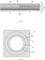
- FIG. 10 shows a diagram of a position of a first hole and a second hole provided in the fourth embodiment of the present application in the area A in FIG. 2 ;
- FIG. 11 shows a structural diagram of a first substrate in the display panel provided in the fourth embodiment of the present application.
- the fourth embodiment of the present application provides a display panel 10.
- the structure of the display panel 10 is similar to that of the display panel 10 in the fourth embodiment of the present application, such as the second substrate 200, and the same parts will not be repeated in this embodiment.
- the difference is that in the display panel 10 provided by the fourth embodiment of the present application, an area of the first hole 161 and an area of the second hole 281 are different.
- the second alignment layer 280 on the second substrate 200 is located in the display area 11 and the transition area 13.
- the second alignment layer 280 is formed with the second hole 281 in the light-transmitting area 12, and an edge of the second hole 281 is located at the boundary of the light-transmitting area 12 and the transition area 13. That is, the edge of the second hole 281 formed in the second alignment layer 280 is the boundary line of the transition area 13 and the light-transmitting area 12; the first alignment layer 160 on the first substrate 100 is located in the display area 11, the transition area 13 and the light-transmitting area 12.
- the first alignment layer 160 is provided with the first hole 161 in the light-transmitting area 12, and an edge of the first hole 161 is located in the light-transmitting area 12. That is, an area of the first hole 161 is smaller than an area of the second hole 281, so that interference and diffraction of light can be reduced, and the imaging result of the optical element disposed on the side of the display panel 10 can be improved.
- FIG. 12 shows an assembly exploded view diagram of the display device provided in the fifth embodiment of the present application.
- the fifth embodiment of the present application provides a display device.
- the display device comprises the display panel 10 in the first to fourth embodiments as aforementioned, a polarizer 20, an optical element 40 and a backlight module 30.
- the display panel 10 comprises: a first substrate 100, a second substrate 200 and a liquid crystal layer 300 disposed between the first substrate 100 and the second substrate 200, and the display panel 10 comprises a light-transmitting area 12 capable of transmitting light;
- the backlight module 30 is arranged on one side of the display panel 10 and is employed to provide the display panel 10 with a light source required for display, and the backlight module 30 is provided with a light-transmitting hole 31 at a position corresponding to the light-transmitting area 12;
- the polarizer 20 comprises a first polarizer 21 and a second polarizer 22 that the polarization axes thereof are perpendicular to each other.
- the first polarizer 21 is disposed on the side of the first substrate 100 away from the liquid crystal layer 300.
- the second polarizer 22 is disposed on the side of the second substrate 200 away from the liquid crystal layer 300.
- the optical element 40 is arranged on the side of the backlight module 30 away from the display panel 10, and is respectively arranged corresponding to the light-transmitting area 12 of the display panel 10 and arranged corresponding to the light-transmitting hole 31 of the backlight module 30.
- the optical element 40 is employed to receive the light that sequentially penetrates the light-transmitting area 12 of the display panel 10 and the light-transmitting hole 31 of the backlight module 30 to realize light sensing and imaging.
- the optical element 40 is, for instance, employed to perform DMS monitoring function.
- the light is infrared light, and the infrared light possesses the function of directly penetrating the first polarizer 21, the liquid crystal layer 300 and the second polarizer 22, and the optical element 40 is correspondingly an infrared camera.
- the infrared camera can well protect user privacy.
- the embodiment of the present application does not limit the type of light and the photosensitive type of the optical element 40.
- the light may also be other than infrared light. Accordingly, the optical element 40 may also possess the function of sensing the other light.
- the present application provides a display panel and a display device.
- the display panel comprises: a first substrate and a second substrate, which are oppositely arranged, and a liquid crystal layer arranged between the first substrate and second substrate, and the first substrate and the second substrate are both provided with an alignment layer on a side close to the liquid crystal layer, wherein the display panel comprises a display area and a light-transmitting area, and at least one of the alignment layers is provided with a hole in the light-transmitting area.
- a hole is provided in at least one alignment layer of the display panel.
- the filtering effect of the alignment layer on the light is greatly reduced, and light loss is reduced, to improve the light transmittance of the area of the display panel corresponding to the optical element. It is to reduce the difficulty for optical elements to collect external ambient light, and increase the amount of light collected by the optical element for improving the imaging result.
Landscapes
- Physics & Mathematics (AREA)
- Nonlinear Science (AREA)
- General Physics & Mathematics (AREA)
- Optics & Photonics (AREA)
- Crystallography & Structural Chemistry (AREA)
- Chemical & Material Sciences (AREA)
- Mathematical Physics (AREA)
- Engineering & Computer Science (AREA)
- Microelectronics & Electronic Packaging (AREA)
- Spectroscopy & Molecular Physics (AREA)
- Health & Medical Sciences (AREA)
- Toxicology (AREA)
- Signal Processing (AREA)
- Devices For Indicating Variable Information By Combining Individual Elements (AREA)
- Liquid Crystal (AREA)
Abstract
Description
- The present application relates to a display field, and more particularly to a display panel and a display device.
- The Liquid Crystal Display (LCD) possesses advantages of high image quality, power saving, thin body and wide application range, stable performance and safety, etc.. Thus, it has been widely applied in various consumer electrical products, such as vehicles, mobile phone, television, personal digital assistant, digital camera, notebook, laptop, and becomes the major display device.
- In the automotive display, the Driver Monitor System (DMS) can monitor the driver's fatigue and improve driving safety. At the same time, with the gradual maturity of autonomous driving, Internet of Vehicles and related technologies, DMS has gradually evolved and iterated more functions, and has gradually been accepted by users. In order to meet the monitoring requirements of DMS, it is necessary to install an optical element on the liquid crystal display. The optical element is a camera for an illustration. For avoiding misunderstandings caused by directly exposing the camera to the user's field of view, the existing LCDs equipped with DMS function mostly adopt the solution of hiding the camera on the back of the LCD panel. However, this solution does not only solve the problem of camera exposure but also enables the camera to perform daylighting function, the external ambient light needs to pass through the LCD panel at least before it can enter the camera smoothly. This greatly increases the difficulty for the camera to collect external ambient light, which directly leads to the problem of insufficient lighting by the camera and poor DMS imaging result, which needs to be solved urgently.
- The present application provides a display panel and a display device thereof, which can increase the light transmittance of the display panel, and reduce the difficulty for optical elements to collect external ambient light, and increase the amount of light collected by the optical element.
- First, the embodiment of the present application provides a display panel, wherein the display panel comprises: a first substrate and a second substrate, which are oppositely arranged, and a liquid crystal layer arranged between the first substrate and second substrate, and the first substrate and the second substrate are both provided with an alignment layer on a side close to the liquid crystal layer, wherein the display panel comprises a display area and a light-transmitting area, and at least one of the alignment layers is provided with a hole in the light-transmitting area.
- Optionally, any one of the alignment layers is provided with a hole in the light-transmitting area.
- Optionally, the hole is filled with an optical film material, and an infrared light transmittance of the optical film material is greater than an infrared light transmittance of the alignment layer.
- Optionally, a visible light reflectivity of the optical film material is less than a visible light reflectivity of the alignment layer.
- Optionally, the alignment layers comprise a first alignment layer provided on the first substrate and a second alignment layer provided on the second substrate, and the first alignment layer is provided with a first hole in the light-transmitting area and the second alignment layer is provided with a second hole in the light-transmitting area, and an area of the first hole and an area of the second hole are the same or different.
- Optionally, the display area and the light-transmitting area are spaced apart, and the display panel further comprises a transition area, and the transition area is located in a gap area between the display area and the light-transmitting area, and a display panel film structure of the transition area is different from a display panel film structure of the display area and a display panel film structure of the light-transmitting area.
- Optionally, the first substrate comprises: a first base substrate and a black matrix layer provided on the first base substrate, and the black matrix layer is located in the display area, and the black matrix layer comprises a black matrix ring located at a boundary of the display area and the transition area.
- Optionally, the first substrate further comprises a color filter layer and a first planarization layer sequentially stacked on the black matrix layer, and the color filter layer is located in the display area, the transition area and the light transmission area, and the first planarization layer is located in the display area, the transition area and the light transmission area, and a thickness of the first planarization layer in the light-transmitting area is greater than a thickness of the first planarization layer in the display area.
- Optionally, the first substrate further comprises the first alignment layer disposed on the first planarization layer, and the first alignment layer is located in the display area and the transition area, and the first alignment layer is provided with the first hole in the light-transmitting area, and an edge of the first hole is located at the boundary of the light-transmitting area and the transition area.
- Optionally, the first substrate further comprises a first optical film material filled in the first hole, and an infrared light transmittance of the first optical film material is greater than an infrared light transmittance of the alignment layer.
- Optionally, the first substrate further comprises a support column layer disposed between the first alignment layer and the first planarization layer, and the support column layer comprises a plurality of support columns arranged at intervals, and the plurality of support columns are located in the display area.
- Optionally, the second substrate comprises: a second base substrate and a thin film transistor layer disposed on the second base substrate, and the thin film transistor layer comprises a thin film transistor and a metal trace, and the thin film transistor is located in the display area and the transition area; the metal trace is located in the display area and the transition area; wherein the metal trace located in the transition area is a ring trace.
- Optionally, the thin film transistor layer further comprises an interlayer dielectric layer disposed on the second base substrate, and the interlayer dielectric layer is located in the display area and the transition area.
- Optionally, the second substrate further comprises a second planarization layer disposed on the interlayer dielectric layer, and the second planarization layer is located in the display area, the transition area and the light-transmitting area, and a thickness of the second planarization layer in the light-transmitting area is greater than a thickness of the second planarization layer in the display area.
- Optionally, the second substrate further comprises a composite film layer disposed on the second planarization layer, and the composite film layer comprises a first transparent conductive layer, a passivation layer and a second transparent conductive layer sequentially stacked on the second planarization layer, and the composite film layer is located in the display area.
- Optionally, the second substrate further comprises a third planarization layer disposed on the composite film layer, and the third planarization layer is located in the display area, the transition area and the light-transmitting area, and a thickness of the third planarization layer in the light-transmitting area is greater than a thickness of the third planarization layer in the display area.
- Optionally, the second substrate further comprises the second alignment layer disposed on the third planarization layer, and the second alignment layer is located in the display area, the transition area, and the light-transmitting area, and the second alignment layer is provided with the second hole in the light-transmitting area, and an edge of the second hole is located in the light-transmitting area.
- Optionally, the second substrate further comprises a second optical film material filled in the second hole, and an infrared light transmittance of the second optical film material is greater than an infrared light transmittance of the alignment layer.
- Second, the embodiment of the present application further provides a display device, wherein the display device comprises: an optical element, a backlight module and the display panel of any one of the above, and the backlight module is arranged on a side of the display panel, and the backlight module is provided with a light-transmitting hole at a position corresponding to the light-transmitting area; the optical element is arranged on a side of the backlight module away from the display panel, and the optical element is arranged corresponding to the light-transmitting hole.
- Optionally, the optical element is an infrared camera.
- Compared with the prior art, the display panel and the display device provided by the present application provide a hole in at least one alignment layer of the display panel. Therefore, when external light enters the optical element through the display panel, the filtering effect of the alignment layer on the light is greatly reduced, and light loss is reduced, to improve the light transmittance of the area of the display panel corresponding to the optical element. It is to reduce the difficulty for optical elements to collect external ambient light, and increase the amount of light collected by the optical element for improving the imaging result of the optical element.
- In order to more clearly illustrate the embodiments of the present application, the following figures will be described in the embodiments are briefly introduced. It is obvious that the drawings are only some embodiments of the present application, those of ordinary skill in this field can obtain other figures according to these figures without paying the premise.
-
FIG. 1 shows a structural diagram of a display panel provided by an embodiment of the present application. -
FIG. 2 shows a top-view diagram of a display panel provided by an embodiment of the present application. -
FIG. 3 shows a structural diagram of a first substrate in the display panel provided in the first embodiment of the present application. -
FIG. 4 shows a diagram of a position of a black matrix ring provided in the first embodiment of the present application in the area A inFIG. 2 . -
FIG. 5 shows a diagram of a position of a first hole and a second hole provided in the first embodiment of the present application in the area A inFIG. 2 . -
FIG. 6 shows a structural diagram of a second substrate in the display panel provided in the first embodiment of the present application. -
FIG. 7 shows a structural diagram of a second substrate in the display panel provided in the second embodiment of the present application. -
FIG. 8 shows a diagram of a position of a first hole and a second hole provided in the third embodiment of the present application in the area A inFIG. 2 . -
FIG. 9 shows a structural diagram of a second substrate in the display panel provided in the third embodiment of the present application. -
FIG. 10 shows a diagram of a position of a first hole and a second hole provided in the fourth embodiment of the present application in the area A inFIG. 2 . -
FIG. 11 shows a structural diagram of a first substrate in the display panel provided in the fourth embodiment of the present application. -
FIG. 12 shows an assembly exploded view diagram of the display device provided in the fifth embodiment of the present application. - Embodiments of the present application are described in detail with the technical matters, structural features, achieved objects, and effects with reference to the accompanying drawings as follows. It is clear that the described embodiments are part of embodiments of the present application, but not all embodiments. Based on the embodiments of the present application, all other embodiments to those of skilled in the premise of no creative efforts obtained, should be considered within the scope of protection of the present application. Besides, it should be understood that the specific embodiments described herein are merely for illustrating and explaining the present application and are not intended to limit the present application. In this application, if no explanation is made to the contrary, the orientation words used such as "upper" and "lower" usually refer to the upper and lower of the device in actual use or working state, which specifically are the directions of the drawing in the figures; and "inner" and "outer" refer to the outline of the device.
- The following disclosure provides many different embodiments or illustrations for implementing different structures of the present application. In order to simplify the disclosure of the present application, the components and arrangements of the specific illustrations are described below. Certainly, they are merely illustrations and are not intended to limit the present application. In addition, the present application may be repeated with reference to the numerals and/or reference numerals in the various embodiments, which are for the purpose of simplicity and clarity, and do not indicate the relationship between the various embodiments and/or arrangements discussed. Moreover, the present application provides illustrations of various specific processes and materials, but one of ordinary skill in the art will recognize the use of other processes and/or the use of other materials. Detailed descriptions are given below. It should be noted that the order of description in the following embodiments is not meant to limit the preferred order of the embodiments.
-
FIG. 1 shows a structural diagram of a display panel provided by an embodiment of the present application. As shown inFIG. 1 , the embodiment of the present application provides adisplay panel 10. Thedisplay panel 10 comprises: afirst substrate 100 and asecond substrate 200. Thefirst substrate 100 and thesecond substrate 200 are oppositely arranged. Thedisplay panel 10 further comprises aliquid crystal layer 300 arranged between thefirst substrate 100 andsecond substrate 200. Liquid crystal molecules are distributed in theliquid crystal layer 300, and the liquid crystal molecules can be twisted under the action of a driving electric field. Thefirst substrate 100 and thesecond substrate 200 are both provided with an alignment layer on a side close to theliquid crystal layer 300. The alignment layer can provide uniformly arranged interface conditions for the liquid crystal molecules, so that the liquid crystal molecules are arranged in a predetermined order. -
FIG. 2 shows a top-view diagram of a display panel provided by an embodiment of the present application. As shown in conjunction withFIGS. 1 and 2 , thedisplay panel 10 comprises: adisplay area 11 and a light-transmittingarea 12. Thedisplay area 11 of thedisplay panel 10 is provided with pixel units and is employed to perform display functions; the light-transmittingarea 12 of thedisplay panel 10 possesses the function of transmitting light, that is, the light transmittance of the light-transmittingarea 12 is higher than the light transmittance of thedisplay area 11. Therefore, when an optical element is disposed on a side of thedisplay panel 10 corresponding to a position of the light-transmittingarea 12, the light can smoothly pass through the light-transmittingarea 12 of thedisplay panel 10 and can be incident on the optical element, so that the optical element normally performs a photosensitive function. - In this embodiment, the alignment layer on the
first substrate 100 is a first alignment layer, and the alignment layer on thesecond substrate 200 is a second alignment layer. The first alignment layer and/or the second alignment layer are provided with holes (not shown in the figure) in the light-transmittingarea 12. Since at least one of the alignment layers is provided with a hole in the light-transmittingarea 12, the filtering effect of the alignment layer on the light penetrating the light-transmittingarea 12 of thedisplay panel 10 can be effectively reduced, and light loss is reduced, to improve the light transmittance of thedisplay panel 10 in the light-transmittingarea 12. Preferably, the first alignment layer and the second alignment layer are both provided with holes in the light-transmittingarea 12, and the hole in the first alignment layer is corresponding to the hole in the second alignment layer. In this embodiment, by providing holes on both two alignment layers of thedisplay panel 10, the light transmittance of thedisplay panel 10 in the light-transmittingarea 12 can be further improved. - In this embodiment, the light is 940 (±10)nm infrared light (Infrared, IR) for instance, and the light transmittance is infrared light transmittance for instance, and the optical element possesses an infrared light sensing function for instance. Since the human body can emit infrared light, when the optical element located on the side of the
display panel 10 and corresponding to the light-transmittingarea 12 collects the infrared light and forms an image, it can well protect user privacy while accomplishing the monitoring requirements of DMS. - In this embodiment, the hole is filled with an optical film material, and a light transmittance of the optical film material is greater than a light transmittance of the alignment layer. By filling the hole with an optical film material with higher light transmittance, it is possible to increase the light transmittance of the
display panel 10 in the light-transmittingarea 12 while filling the hole in the alignment layer to achieve planarization. - In this embodiment, a visible light reflectivity of the optical film material is less than a visible light reflectivity of the alignment layer. Since the visible light reflectivity of the optical film material is less than the visible light reflectivity of the alignment layer, the uniform display effect of the
display panel 10 can be improved, and the display quality can be improved. - In this embodiment, the optical film material is, for instance, an antireflective film, and the antireflective film is filled in the hole of the alignment layer. The antireflective film can reduce the reflectivity of visible light in the
display panel 10 and increase the transmittance of infrared light in thedisplay panel 10. - Continuing to refer to
FIG. 2 , in this embodiment, thedisplay area 11 and the light-transmittingarea 12 are spaced apart, and thedisplay panel 10 further comprises atransition area 13, and thetransition area 13 is located in a gap area between thedisplay area 11 and the light-transmittingarea 12, and a display panel film structure of thetransition area 13 is different from a display panel film structure of thedisplay area 11 and a display panel film structure of the light-transmittingarea 12, and the alignment layer is at least disposed in thetransition area 13 of thedisplay panel 10. Correspondingly, since the gap area between thedisplay area 11 and the light-transmittingarea 12 is also provided with an alignment layer, the liquid crystal molecules located near the boundary area of thedisplay area 11 and thetransition area 13 can have the same alignment form as the liquid crystal molecules located in thedisplay area 11 to ensure the display effect of thedisplay area 11. - In this embodiment, the
transition area 13 surrounds the light-transmittingarea 12, and thedisplay area 11 surrounds thetransition area 13. - In this embodiment, the
display panel 10 further comprises, for instance, a non-display area, and the non-display area is adjacent to thedisplay area 11, and the non-display area is arranged around thedisplay area 11. -
FIG. 3 shows a structural diagram of a first substrate in the display panel provided in the first embodiment of the present application;FIG. 4 shows a diagram of a position of a black matrix ring provided in the first embodiment of the present application in the area A inFIG. 2 ;FIG. 5 shows a diagram of a position of a first hole and a second hole provided in the first embodiment of the present application in the area A inFIG. 2 ;FIG. 6 shows a structural diagram of a second substrate in the display panel provided in the first embodiment of the present application. The specific film structure of thefirst substrate 100 and thesecond substrate 200 in thedisplay panel 10 will be described in detail below with reference toFIGS. 3 to 6 . - In this embodiment, the alignment layers comprise a
first alignment layer 160 provided on thefirst substrate 100 and asecond alignment layer 280 provided on thesecond substrate 200, and thefirst alignment layer 160 is provided with afirst hole 161 in the light-transmittingarea 12 and thesecond alignment layer 280 is provided with asecond hole 281 in the light-transmittingarea 12, and an area of thefirst hole 161 and an area of thesecond hole 281 are the same. - In this embodiment, the
first substrate 100 comprises: afirst base substrate 110. Thefirst base substrate 110 is a carrier of other film structures on thefirst substrate 100, which can be a rigid substrate or a flexible substrate, and its material can be glass, plastic, or other inorganic or organic materials with excellent light transmittance. Preferably, thefirst base substrate 110 is a rigid glass substrate. - In this embodiment, the
first substrate 100 further comprises ablack matrix layer 120 provided on thefirst base substrate 110, and theblack matrix layer 120 is located in thedisplay area 11. That is, theblack matrix layer 120 is not provided in the light-transmittingarea 12. Since the light-transmittingarea 12 omits theblack matrix layer 120 with low light transmittance, the light transmittance of thedisplay panel 10 can be further improved. Specifically, theblack matrix layer 120 located in thedisplay area 11 is formed with a grid-shapedblack matrix structure 121. The infrared light transmittance of theblack matrix structure 121 is 0%. Since thefirst substrate 100 is not provided with theblack matrix structure 121 in the light-transmittingarea 12, the light transmittance of the infrared light of the light-transmittingarea 12 can be greatly improved. Furthermore, theblack matrix layer 121 comprises ablack matrix ring 1211 located at a boundary of thedisplay area 11 and thetransition area 13. That is, theblack matrix ring 1211 is the boundary line of thedisplay area 11 and thetransition area 13. - In this embodiment, the
first substrate 100 further comprises acolor filter layer 130 and afirst planarization layer 140 sequentially stacked on theblack matrix layer 120, and thecolor filter layer 130 is located in thedisplay area 11, thetransition area 13 and thelight transmission area 12, and thefirst planarization layer 140 is located in thedisplay area 11, thetransition area 13 and thelight transmission area 12, and a thickness of thefirst planarization layer 140 in the light-transmittingarea 12 is greater than a thickness of thefirst planarization layer 140 in thedisplay area 11. Specifically, thecolor filter layer 130 located in thedisplay area 11, thetransition area 13 and the light-transmittingarea 12 is formed by the same process, and thecolor filter layer 130 of thedisplay area 11 comprises color resist units of multiple colors, and the color resist units are used to realize a color display function; thefirst planarization layer 140 located in thedisplay area 11, thetransition area 13 and the light-transmittingarea 12 is formed by the same process, and the surface of thefirst planarization layer 140 away from thefirst base substrate 110 is a planar surface for achieving a planarizing function. The infrared light transmittance of thecolor filter layer 130 is 98%, and the infrared light transmittance of thefirst planarization layer 140 is 100%. Since the infrared light transmittance of thecolor filter layer 130 and thefirst planarization layer 140 are both relatively high, both thecolor filter layer 130 and thefirst planarization layer 140 remain in thedisplay area 11 and the light-transmittingarea 12. - In this embodiment, the
first substrate 100 further comprises afirst alignment layer 160 disposed on thefirst planarization layer 140, and thefirst alignment layer 160 is located in thedisplay area 11 and thetransition area 13, and thefirst alignment layer 160 is provided with thefirst hole 161 in the light-transmittingarea 12, and an edge of thefirst hole 161 is located at the boundary of the light-transmittingarea 12 and thetransition area 13. That is, the edge of thefirst hole 161 formed in thefirst alignment layer 160 is the boundary line of thetransition area 13 and the light-transmittingarea 12. The infrared light transmittance of thefirst alignment layer 160 is 92%. Since thefirst alignment layer 160 is omitted in the light-transmittingarea 12, the infrared light transmittance of the light-transmittingarea 12 can be greatly improved. - In this embodiment, the
first substrate 100 further comprises a firstoptical film material 170 filled in thefirst hole 161, and an infrared light transmittance of the firstoptical film material 170 is greater than an infrared light transmittance of thealignment layer 160. Since thefirst substrate 100 is formed with the firstoptical film material 170 with higher light transmittance in the area corresponding to the light-transmittingarea 12, the infrared light transmittance of thedisplay panel 10 in the light-transmittingarea 12 can be effectively improved. - In this embodiment, a visible light reflectivity of the first
optical film material 170 is less than a visible light reflectivity of thefirst alignment layer 160. By reducing the visible light reflectivity of the firstoptical film material 170, the uniform display effect of thedisplay panel 10 can be improved, and the display quality of thedisplay panel 10 can be improved. - In this embodiment, the first
optical film material 170 is, for instance, an antireflective film, and the antireflective film is filled in thefirst hole 161 of the alignment layer 160.The antireflective film can reduce the reflectivity of visible light in thedisplay panel 10 and increase the transmittance of infrared light in thedisplay panel 10. - In this embodiment, the
first substrate 100 further comprises asupport column layer 150 disposed between thefirst alignment layer 160 and thefirst planarization layer 140, and thesupport column layer 150 comprises a plurality of support columns arranged at intervals. The support columns can form a stable separation distance between thefirst substrate 100 and thesecond substrate 200 to ensure the normal display of thedisplay panel 10. Specifically, the plurality of support columns is located in thedisplay area 11. That is, the support columns are not arranged in the light-transmittingarea 12. Since the support column will diffract the infrared light, which will affect the imaging result of the optical element located on the side of the display panel, the support column is not provided in the light-transmittingarea 12 in the present application. Therefore, the infrared light transmittance of thedisplay panel 10 in the light-transmittingarea 12 can be further improved, while the diffraction phenomenon can be avoided, and the imaging result of the optical element can be improved. - In this embodiment, the
second substrate 200 comprises: asecond base substrate 210 and a thin film transistor layer disposed on thesecond base substrate 210, and the thin film transistor layer comprises a thin film transistor and a metal trace, and the thin film transistor is located in thedisplay area 11 and thetransition area 13; the metal trace is located in thedisplay area 11 and thetransition area 13. That is, the light-transmittingarea 12 is not provided with the thin film transistor and the metal trace. The thin film transistor and the metal trace generally comprise opaque metal material. Since the light-transmittingarea 12 is not provided with the thin film transistor and the metal trace, the infrared light transmittance of thedisplay panel 10 in the light-transmittingarea 12 can be further improved. - In this embodiment, the thin film transistor is, for instance, low temperature polysilicon thin film transistor. The thin film transistor comprises various film layers. The various film layers comprise, for instance, a light-shielding layer, a buffer layer, a first metal layer, a gate insulating layer, an active layer, an
interlayer dielectric layer 220 and a second metal layer that are sequentially stacked on thesecond base substrate 210. The light-shielding layer comprises a light-shielding pattern corresponding to a channel region of the active layer, and the light-shielding layer is located in the display area 11 and the transition area 13; the buffer layer is a laminated structure formed by a silicon nitride film layer and a silicon oxide film layer, and the buffer layer is located in the display area 11, the transition area 13 and the light-transmitting area 12; the first metal layer comprises a gate and metal trace, and the first metal layer is located in the display area 11 and the transition area 13; the gate insulating layer is a silicon oxide film layer, and the gate insulating layer is located in the display area 11, the transition area 13 and the light-transmitting area 12; the active layer comprises a channel region, a heavily doped region and a lightly doped region, and the active layer is located in the display area 11 and the transition area 13; the interlayer dielectric layer 220 is a laminated structure formed by a silicon nitride film layer and a silicon oxide film layer, and the interlayer dielectric layer 220 is located in the display area 11, the transition area 13 and the light-transmitting area 12; the second metal layer comprises a source, a drain and a metal trace, and the second metal layer is located in the display area 11 and the transition area 13. Certainly, the embodiment of the present application does not limit the type of the thin film transistor, and the type of the thin film transistor may also be an amorphous silicon thin film transistor or an oxide thin film transistor. - In this embodiment, the
second substrate 200 further comprises asecond planarization layer 230 disposed on theinterlayer dielectric layer 220, and thesecond planarization layer 230 is located in thedisplay area 11, thetransition area 13 and the light-transmittingarea 12. Specifically, thesecond planarization layer 230 located in thedisplay area 11, thetransition area 13 and the light-transmittingarea 12 is formed by the same process, and the surface of thesecond planarization layer 230 away from thesecond base substrate 210 is a planar surface for achieving a planarizing function. - In this embodiment, the
second substrate 200 further comprises a composite film layer disposed on thesecond planarization layer 230, and the composite film layer comprises a first transparentconductive layer 240, apassivation layer 250 and a second transparentconductive layer 260 sequentially stacked on thesecond planarization layer 230, and the composite film layer is located in thedisplay area 11. That is, the light-transmittingarea 12 is not provided with the composite film layer, so that the infrared light transmittance of thedisplay panel 10 in the light-transmittingarea 12 can be further improved. Specifically, the material for forming the first transparentconductive layer 240 and the second transparentconductive layer 260 is indium tin oxide (ITO), and the material for forming thepassivation layer 250 is silicon nitride. The infrared light transmittance of the composite film layer is 72%. Since the composite film layer is not provided in the light-transmittingarea 12, the infrared light transmittance of thedisplay panel 10 in the light-transmittingarea 12 can be significantly improved. - In this embodiment, the
second substrate 200 further comprises athird planarization layer 270 disposed on the composite film layer, and thethird planarization layer 270 is located in thedisplay area 11, thetransition area 13 and the light-transmittingarea 12, and a thickness of thethird planarization layer 270 in the light-transmittingarea 12 is greater than a thickness of thethird planarization layer 270 in thedisplay area 11. Specifically, thethird planarization layer 270 located in thedisplay area 11, thetransition area 13 and the light-transmittingarea 12 is formed by the same process, and the surface of thethird planarization layer 270 away from thesecond base substrate 210 is a planar surface for achieving a planarizing function. - In this embodiment, the
second substrate 200 further comprises thesecond alignment layer 280 disposed on thethird planarization layer 270, and thesecond alignment layer 280 is located in thedisplay area 11 and thetransition area 13, and thesecond alignment layer 280 is provided with thesecond hole 281 in the boundary area of the light-transmittingarea 12 and thetransition area 13. That is, the edge of thesecond hole 281 formed in thesecond alignment layer 280 is the boundary line of thetransition area 13 and the light-transmittingarea 12. Thesecond alignment layer 280 is provided with thesecond hole 281 in the light-transmittingarea 12, and an edge of thesecond hole 281 is located at the boundary of the light-transmittingarea 12 and thetransition area 13. That is, the edge of thesecond hole 281 formed in thesecond alignment layer 280 is the boundary line of thetransition area 13 and the light-transmittingarea 12, and an area of thesecond hole 281 is equal to an area of thefirst hole 161. The infrared light transmittance of thesecond alignment layer 280 is 92%. Since thesecond alignment layer 280 is omitted in the light-transmittingarea 12, the infrared light transmittance of the light-transmittingarea 12 can be greatly improved. - In this embodiment, the
second substrate 200 further comprises a secondoptical film material 290 filled in thesecond hole 281, and an infrared light transmittance of the secondoptical film material 290 is greater than an infrared light transmittance of thealignment layer 280. Since thesecond substrate 200 is formed with the secondoptical film material 290 with higher light transmittance in the area corresponding to the light-transmittingarea 12, the infrared light transmittance of thedisplay panel 10 in the light-transmittingarea 12 can be effectively improved. - In this embodiment, a visible light reflectivity of the second
optical film material 290 is less than a visible light reflectivity of thesecond alignment layer 280. By reducing the visible light reflectivity of the secondoptical film material 290, the uniform display effect of thedisplay panel 10 can be improved, and the display quality of thedisplay panel 10 can be improved. - In this embodiment, the second
optical film material 290 is, for instance, an antireflective film, and the antireflective film is filled in thesecond hole 281 of thesecond alignment layer 280. The antireflective film can reduce the reflectivity of visible light in thedisplay panel 10 and increase the transmittance of infrared light in thedisplay panel 10. -
FIG. 7 shows a structural diagram of a second substrate in the display panel provided in the second embodiment of the present application. As shown inFIG. 7 , the second embodiment of the present application provides adisplay panel 10. The structure of thedisplay panel 10 is similar to that of thedisplay panel 10 in the first embodiment of the present application, and the same parts will not be repeated in this embodiment. - The difference is that in the
display panel 10 provided by the second embodiment of the present application, theinterlayer dielectric layer 220 is located in thedisplay area 11 and thetransition area 13, that is, theinterlayer dielectric layer 220 is not located in the light-transmittingarea 12. Therefore, the film structure of the light-transmittingarea 12 is simplified, and the number of film layers is reduced, and the infrared light transmittance of thedisplay panel 10 in the light-transmittingarea 12 can be further improved. - Moreover, the
second substrate 200 further comprises asecond planarization layer 230 disposed on theinterlayer dielectric layer 220, and thesecond planarization layer 230 is located in thedisplay area 11, thetransition area 13 and the light-transmittingarea 12, and a thickness of thesecond planarization layer 230 in the light-transmittingarea 12 is greater than a thickness of thesecond planarization layer 230 in thedisplay area 11. Specifically, thesecond planarization layer 230 located in thedisplay area 11, thetransition area 13 and the light-transmittingarea 12 is formed by the same process, and the surface of thesecond planarization layer 230 away from thesecond base substrate 210 is a planar surface for achieving a planarizing function. -
FIG. 8 shows a diagram of a position of a first hole and a second hole provided in the third embodiment of the present application in the area A inFIG. 2 ;FIG. 9 shows a structural diagram of a second substrate in the display panel provided in the third embodiment of the present application. As shown inFIG. 3 ,FIG. 8 andFIG. 9 , the third embodiment of the present application provides adisplay panel 10. Thedisplay panel 10 is similar in structure to thedisplay panel 10 in the first embodiment of the present application. For instance, the structure of thefirst substrate 100 in the third embodiment is the same as that of thefirst substrate 100 in the first embodiment, and the same parts will not be repeated in this embodiment. - The difference is that in the
display panel 10 provided by the third embodiment of the present application, an area of thefirst hole 161 and an area of thesecond hole 281 are different. Specifically, thefirst alignment layer 160 on thefirst substrate 100 is located in thedisplay area 11 and thetransition area 13, and thefirst alignment layer 160 is provided with thefirst hole 161 in the light-transmittingarea 12, and an edge of thefirst hole 161 is located at the boundary of the light-transmittingarea 12 and thetransition area 13. That is, the edge of thefirst hole 161 formed in thefirst alignment layer 160 is the boundary line of thetransition area 13 and the light-transmittingarea 12; thesecond alignment layer 280 on thesecond substrate 200 is located in thedisplay area 11, thetransition area 13 and the light-transmittingarea 12. Thesecond alignment layer 280 is provided with thesecond hole 281 in the light-transmittingarea 12, and an edge of thesecond hole 281 is located in the light-transmittingarea 12. That is, an area of thesecond hole 281 is smaller than an area of thefirst hole 161, so that interference and diffraction of light can be reduced, and the imaging result of the optical element disposed on the side of thedisplay panel 10 can be improved. -
FIG. 10 shows a diagram of a position of a first hole and a second hole provided in the fourth embodiment of the present application in the area A inFIG. 2 ;FIG. 11 shows a structural diagram of a first substrate in the display panel provided in the fourth embodiment of the present application. As shown inFIG. 6 ,FIG. 10 andFIG. 11 , the fourth embodiment of the present application provides adisplay panel 10. The structure of thedisplay panel 10 is similar to that of thedisplay panel 10 in the fourth embodiment of the present application, such as thesecond substrate 200, and the same parts will not be repeated in this embodiment. - The difference is that in the
display panel 10 provided by the fourth embodiment of the present application, an area of thefirst hole 161 and an area of thesecond hole 281 are different. Specifically, thesecond alignment layer 280 on thesecond substrate 200 is located in thedisplay area 11 and thetransition area 13. Thesecond alignment layer 280 is formed with thesecond hole 281 in the light-transmittingarea 12, and an edge of thesecond hole 281 is located at the boundary of the light-transmittingarea 12 and thetransition area 13. That is, the edge of thesecond hole 281 formed in thesecond alignment layer 280 is the boundary line of thetransition area 13 and the light-transmittingarea 12; thefirst alignment layer 160 on thefirst substrate 100 is located in thedisplay area 11, thetransition area 13 and the light-transmittingarea 12. Thefirst alignment layer 160 is provided with thefirst hole 161 in the light-transmittingarea 12, and an edge of thefirst hole 161 is located in the light-transmittingarea 12. That is, an area of thefirst hole 161 is smaller than an area of thesecond hole 281, so that interference and diffraction of light can be reduced, and the imaging result of the optical element disposed on the side of thedisplay panel 10 can be improved. -
FIG. 12 shows an assembly exploded view diagram of the display device provided in the fifth embodiment of the present application. As shown inFIG. 12 , the fifth embodiment of the present application provides a display device. The display device comprises thedisplay panel 10 in the first to fourth embodiments as aforementioned, apolarizer 20, anoptical element 40 and abacklight module 30. Thedisplay panel 10 comprises: afirst substrate 100, asecond substrate 200 and aliquid crystal layer 300 disposed between thefirst substrate 100 and thesecond substrate 200, and thedisplay panel 10 comprises a light-transmittingarea 12 capable of transmitting light; thebacklight module 30 is arranged on one side of thedisplay panel 10 and is employed to provide thedisplay panel 10 with a light source required for display, and thebacklight module 30 is provided with a light-transmittinghole 31 at a position corresponding to the light-transmittingarea 12; Thepolarizer 20 comprises afirst polarizer 21 and asecond polarizer 22 that the polarization axes thereof are perpendicular to each other. Thefirst polarizer 21 is disposed on the side of thefirst substrate 100 away from theliquid crystal layer 300. Thesecond polarizer 22 is disposed on the side of thesecond substrate 200 away from theliquid crystal layer 300. - In this embodiment, the
optical element 40 is arranged on the side of thebacklight module 30 away from thedisplay panel 10, and is respectively arranged corresponding to the light-transmittingarea 12 of thedisplay panel 10 and arranged corresponding to the light-transmittinghole 31 of thebacklight module 30. Theoptical element 40 is employed to receive the light that sequentially penetrates the light-transmittingarea 12 of thedisplay panel 10 and the light-transmittinghole 31 of thebacklight module 30 to realize light sensing and imaging. Theoptical element 40 is, for instance, employed to perform DMS monitoring function. The light is infrared light, and the infrared light possesses the function of directly penetrating thefirst polarizer 21, theliquid crystal layer 300 and thesecond polarizer 22, and theoptical element 40 is correspondingly an infrared camera. The infrared camera can well protect user privacy. However, it should be noted that the embodiment of the present application does not limit the type of light and the photosensitive type of theoptical element 40. The light may also be other than infrared light. Accordingly, theoptical element 40 may also possess the function of sensing the other light. - In conclusion, the present application provides a display panel and a display device. The display panel comprises: a first substrate and a second substrate, which are oppositely arranged, and a liquid crystal layer arranged between the first substrate and second substrate, and the first substrate and the second substrate are both provided with an alignment layer on a side close to the liquid crystal layer, wherein the display panel comprises a display area and a light-transmitting area, and at least one of the alignment layers is provided with a hole in the light-transmitting area. In the present application, a hole is provided in at least one alignment layer of the display panel. Therefore, when external light enters the optical element through the display panel, the filtering effect of the alignment layer on the light is greatly reduced, and light loss is reduced, to improve the light transmittance of the area of the display panel corresponding to the optical element. It is to reduce the difficulty for optical elements to collect external ambient light, and increase the amount of light collected by the optical element for improving the imaging result.
- The display panel and the display device provided by the embodiments of the present application are described in detail as aforementioned, and the principles and implementations of the present application have been described with reference to specific illustrations. The description of the foregoing embodiments is merely for helping to understand the technical solutions of the present application and the core ideas thereof; meanwhile, those skilled in the art will be able to change the specific embodiments and the scope of the application according to the idea of the present application. In conclusion, the content of the specification should not be construed as limiting the present application.
Claims (20)
- A display panel, wherein the display panel comprises: a first substrate and a second substrate, which are oppositely arranged, and a liquid crystal layer arranged between the first substrate and second substrate, and the first substrate and the second substrate are both provided with an alignment layer on a side close to the liquid crystal layer, wherein the display panel comprises a display area and a light-transmitting area, and at least one of the alignment layers is provided with a hole in the light-transmitting area.
- The display panel according to claim 1, wherein any one of the alignment layers is provided with a hole in the light-transmitting area.
- The display panel according to claim 1, wherein the hole is filled with an optical film material, and an infrared light transmittance of the optical film material is greater than an infrared light transmittance of the alignment layer.
- The display panel according to claim 3, wherein a visible light reflectivity of the optical film material is less than a visible light reflectivity of the alignment layer.
- The display panel according to claim 1, wherein the alignment layers comprise a first alignment layer provided on the first substrate and a second alignment layer provided on the second substrate, and the first alignment layer is provided with a first hole in the light-transmitting area and the second alignment layer is provided with a second hole in the light-transmitting area, and an area of the first hole and an area of the second hole are the same or different.
- The display panel according to claim 5, wherein the display area and the light-transmitting area are spaced apart, and the display panel further comprises a transition area, and the transition area is located in a gap area between the display area and the light-transmitting area, and a display panel film structure of the transition area is different from a display panel film structure of the display area and a display panel film structure of the light-transmitting area.
- The display panel according to claim 6, wherein the first substrate comprises: a first base substrate and a black matrix layer provided on the first base substrate, and the black matrix layer is located in the display area, and the black matrix layer comprises a black matrix ring located at a boundary of the display area and the transition area.
- The display panel according to claim 7, wherein the first substrate further comprises a color filter layer and a first planarization layer sequentially stacked on the black matrix layer, and the color filter layer is located in the display area, the transition area and the light transmission area, and the first planarization layer is located in the display area, the transition area and the light transmission area, and a thickness of the first planarization layer in the light-transmitting area is greater than a thickness of the first planarization layer in the display area.
- The display panel according to claim 8, wherein the first substrate further comprises the first alignment layer disposed on the first planarization layer, and the first alignment layer is located in the display area and the transition area, and the first alignment layer is provided with the first hole in the light-transmitting area, and an edge of the first hole is located at the boundary of the light-transmitting area and the transition area.
- The display panel according to claim 9, wherein the first substrate further comprises a first optical film material filled in the first hole, and an infrared light transmittance of the first optical film material is greater than an infrared light transmittance of the alignment layer.
- The display panel according to claim 9, wherein the first substrate further comprises a support column layer disposed between the first alignment layer and the first planarization layer, and the support column layer comprises a plurality of support columns arranged at intervals, and the plurality of support columns are located in the display area.
- The display panel according to claim 6, wherein the second substrate comprises: a second base substrate and a thin film transistor layer disposed on the second base substrate, and the thin film transistor layer comprises a thin film transistor and a metal trace, and the thin film transistor is located in the display area and the transition area; the metal trace is located in the display area and the transition area; wherein the metal trace located in the transition area is a ring trace.
- The display panel according to claim 12, wherein the thin film transistor layer further comprises an interlayer dielectric layer disposed on the second base substrate, and the interlayer dielectric layer is located in the display area and the transition area.
- The display panel according to claim 13, wherein the second substrate further comprises a second planarization layer disposed on the interlayer dielectric layer, and the second planarization layer is located in the display area, the transition area and the light-transmitting area, and a thickness of the second planarization layer in the light-transmitting area is greater than a thickness of the second planarization layer in the display area.
- The display panel according to claim 14, wherein the second substrate further comprises a composite film layer disposed on the second planarization layer, and the composite film layer comprises a first transparent conductive layer, a passivation layer and a second transparent conductive layer sequentially stacked on the second planarization layer, and the composite film layer is located in the display area.
- The display panel according to claim 15, wherein the second substrate further comprises a third planarization layer disposed on the composite film layer, and the third planarization layer is located in the display area, the transition area and the light-transmitting area, and a thickness of the third planarization layer in the light-transmitting area is greater than a thickness of the third planarization layer in the display area.
- The display panel according to claim 16, wherein the second substrate further comprises the second alignment layer disposed on the third planarization layer, and the second alignment layer is located in the display area, the transition area, and the light-transmitting area, and the second alignment layer is provided with the second hole in the light-transmitting area, and an edge of the second hole is located in the light-transmitting area.
- The display panel according to claim 17, wherein the second substrate further comprises a second optical film material filled in the second hole, and an infrared light transmittance of the second optical film material is greater than an infrared light transmittance of the alignment layer.
- A display device, wherein the display device comprises: an optical element, a backlight module and the display panel according to claim 1, and the backlight module is arranged on a side of the display panel, and the backlight module is provided with a light-transmitting hole at a position corresponding to the light-transmitting area; the optical element is arranged on a side of the backlight module away from the display panel, and the optical element is arranged corresponding to the light-transmitting hole.
- The display device according to claim 19, wherein the optical element is an infrared camera.
Applications Claiming Priority (2)
| Application Number | Priority Date | Filing Date | Title |
|---|---|---|---|
| CN202111348662.4A CN114047650B (en) | 2021-11-15 | 2021-11-15 | Display panel and display device |
| PCT/CN2021/134122 WO2023082364A1 (en) | 2021-11-15 | 2021-11-29 | Display panel and display apparatus |
Publications (2)
| Publication Number | Publication Date |
|---|---|
| EP4435507A1 true EP4435507A1 (en) | 2024-09-25 |
| EP4435507A4 EP4435507A4 (en) | 2025-09-24 |
Family
ID=80209160
Family Applications (1)
| Application Number | Title | Priority Date | Filing Date |
|---|---|---|---|
| EP21827536.0A Pending EP4435507A4 (en) | 2021-11-15 | 2021-11-29 | Display panel and display apparatus |
Country Status (6)
| Country | Link |
|---|---|
| US (1) | US12197083B2 (en) |
| EP (1) | EP4435507A4 (en) |
| JP (1) | JP7494219B2 (en) |
| KR (1) | KR102796132B1 (en) |
| CN (2) | CN117784475B (en) |
| WO (1) | WO2023082364A1 (en) |
Families Citing this family (1)
| Publication number | Priority date | Publication date | Assignee | Title |
|---|---|---|---|---|
| CN117784475B (en) * | 2021-11-15 | 2025-11-21 | 武汉华星光电技术有限公司 | Display panel and display device |
Family Cites Families (21)
| Publication number | Priority date | Publication date | Assignee | Title |
|---|---|---|---|---|
| JPH09127525A (en) | 1995-11-06 | 1997-05-16 | Sharp Corp | Liquid crystal display device and method of manufacturing the same |
| JP4536489B2 (en) * | 2004-11-15 | 2010-09-01 | 株式会社 日立ディスプレイズ | Optical element and display device using the same |
| WO2014141893A1 (en) | 2013-03-15 | 2014-09-18 | シャープ株式会社 | Electronic device |
| KR102342609B1 (en) * | 2017-04-25 | 2021-12-22 | 후아웨이 테크놀러지 컴퍼니 리미티드 | Lcd display screen, electronic device, manufacturing method for lcd display screen |
| CN107946341B (en) | 2017-11-10 | 2020-05-22 | 上海天马微电子有限公司 | Display device and method for manufacturing display device |
| JP2019184827A (en) * | 2018-04-10 | 2019-10-24 | シャープ株式会社 | Liquid crystal display and method for manufacturing the same |
| EP3828624B1 (en) * | 2018-09-12 | 2025-11-26 | Huawei Technologies Co., Ltd. | Liquid crystal display panel |
| CN109164648B (en) * | 2018-09-30 | 2021-11-19 | 厦门天马微电子有限公司 | Display panel and display device |
| CN109283722A (en) * | 2018-09-30 | 2019-01-29 | 厦门天马微电子有限公司 | A kind of display panel and preparation method thereof, display device |
| CN111142281A (en) | 2018-11-05 | 2020-05-12 | 华为终端有限公司 | A display panel and preparation method thereof, mobile terminal and preparation method thereof |
| CN211180468U (en) | 2018-12-07 | 2020-08-04 | 鸿富锦精密工业(深圳)有限公司 | Display panel and display device |
| CN111508349B (en) * | 2019-01-31 | 2022-03-08 | 武汉华星光电半导体显示技术有限公司 | Display panel, manufacturing method of display panel and electronic equipment |
| CN109856850B (en) * | 2019-03-29 | 2020-10-13 | 武汉华星光电技术有限公司 | Display device |
| KR102830618B1 (en) * | 2019-12-31 | 2025-07-08 | 삼성디스플레이 주식회사 | Display apparatus |
| CN111273476A (en) * | 2020-03-27 | 2020-06-12 | 武汉华星光电技术有限公司 | Display panel, manufacturing method thereof and display device |
| CN111965872B (en) * | 2020-08-05 | 2022-02-22 | 武汉华星光电技术有限公司 | Display panel and display device |
| CN111983838A (en) | 2020-08-20 | 2020-11-24 | 武汉华星光电技术有限公司 | Display panel and manufacturing method thereof |
| CN112180633A (en) | 2020-10-22 | 2021-01-05 | 武汉华星光电技术有限公司 | Display module and display device |
| CN112259595B (en) * | 2020-10-30 | 2022-10-11 | 武汉天马微电子有限公司 | Array substrate and display panel |
| CN112509468A (en) | 2020-11-27 | 2021-03-16 | 武汉华星光电半导体显示技术有限公司 | Display module, preparation method thereof and display device |
| CN117784475B (en) * | 2021-11-15 | 2025-11-21 | 武汉华星光电技术有限公司 | Display panel and display device |
-
2021
- 2021-11-15 CN CN202410026532.6A patent/CN117784475B/en active Active
- 2021-11-15 CN CN202111348662.4A patent/CN114047650B/en active Active
- 2021-11-29 KR KR1020227013205A patent/KR102796132B1/en active Active
- 2021-11-29 WO PCT/CN2021/134122 patent/WO2023082364A1/en not_active Ceased
- 2021-11-29 EP EP21827536.0A patent/EP4435507A4/en active Pending
- 2021-11-29 US US17/619,551 patent/US12197083B2/en active Active
- 2021-11-29 JP JP2021573227A patent/JP7494219B2/en active Active
Also Published As
| Publication number | Publication date |
|---|---|
| JP7494219B2 (en) | 2024-06-03 |
| CN114047650B (en) | 2023-12-22 |
| CN114047650A (en) | 2022-02-15 |
| WO2023082364A1 (en) | 2023-05-19 |
| EP4435507A4 (en) | 2025-09-24 |
| KR20230071768A (en) | 2023-05-23 |
| US12197083B2 (en) | 2025-01-14 |
| JP2024503153A (en) | 2024-01-25 |
| US20240045271A1 (en) | 2024-02-08 |
| CN117784475B (en) | 2025-11-21 |
| CN117784475A (en) | 2024-03-29 |
| KR102796132B1 (en) | 2025-04-16 |
Similar Documents
| Publication | Publication Date | Title |
|---|---|---|
| CN113359344B (en) | Array substrate, liquid crystal display panel and liquid crystal display device | |
| JP3485997B2 (en) | Liquid crystal display | |
| US8553194B2 (en) | Liquid crystal display device, liquid crystal display device manufacturing method, and electronic device | |
| US6954241B2 (en) | Color filter substrate, method for manufacturing the same, liquid crystal display panel, and electronic equipment | |
| KR20130108574A (en) | Array substrate, manufacturing method thereof, and display device | |
| TW200300861A (en) | Liquid crystal display device, substrate for liquid crystal display device, and electronic apparatus | |
| KR20110133836A (en) | Color filter display panel and flat panel display device including the same | |
| TWI469360B (en) | Display panel and display device | |
| US20140002777A1 (en) | Reflective liquid crystal displays and methods of fabricating the same | |
| JP4924224B2 (en) | Photodetector built-in display device and electronic device | |
| KR102643383B1 (en) | Liquid crystal display panel and vehicle liquid crystal display device | |
| US12197083B2 (en) | Display panel and display device | |
| JP2009139853A (en) | Liquid crystal display device | |
| CN113391485A (en) | Array substrate, manufacturing method and display panel | |
| US7646440B2 (en) | Pixel structure of LCD and fabrication method thereof | |
| KR20040011382A (en) | Liquid crystal display device | |
| JP2008020772A (en) | Liquid crystal display panel | |
| US20120104441A1 (en) | Method of manufacturing color filter substrate, semi-transmissive liquid crystal display using the same, and manufacturing method thereof | |
| US20190056622A1 (en) | Transflective liquid crystal display and manufacturing method thereof | |
| US20190064616A1 (en) | Transflective liquid crystal display | |
| US20100127272A1 (en) | Thin film transistor array panel and manufacturing method thereof | |
| CN113985663A (en) | Display panel, display device and vehicle-mounted monitoring device | |
| JP2004233959A (en) | Liquid crystal display | |
| JP4337807B2 (en) | Liquid crystal device and electronic device | |
| EA050393B1 (en) | DISPLAY PANEL AND DISPLAY DEVICE |
Legal Events
| Date | Code | Title | Description |
|---|---|---|---|
| STAA | Information on the status of an ep patent application or granted ep patent |
Free format text: STATUS: UNKNOWN |
|
| STAA | Information on the status of an ep patent application or granted ep patent |
Free format text: STATUS: THE INTERNATIONAL PUBLICATION HAS BEEN MADE |
|
| PUAI | Public reference made under article 153(3) epc to a published international application that has entered the european phase |
Free format text: ORIGINAL CODE: 0009012 |
|
| STAA | Information on the status of an ep patent application or granted ep patent |
Free format text: STATUS: REQUEST FOR EXAMINATION WAS MADE |
|
| 17P | Request for examination filed |
Effective date: 20211229 |
|
| AK | Designated contracting states |
Kind code of ref document: A1 Designated state(s): AL AT BE BG CH CY CZ DE DK EE ES FI FR GB GR HR HU IE IS IT LI LT LU LV MC MK MT NL NO PL PT RO RS SE SI SK SM TR |
|
| DAV | Request for validation of the european patent (deleted) | ||
| DAX | Request for extension of the european patent (deleted) | ||
| A4 | Supplementary search report drawn up and despatched |
Effective date: 20250827 |
|
| RIC1 | Information provided on ipc code assigned before grant |
Ipc: G02F 1/1337 20060101AFI20250821BHEP |