EP4432011A1 - Verfahren zur bildung eines resistunterschichtfilms und strukturierungsverfahren - Google Patents
Verfahren zur bildung eines resistunterschichtfilms und strukturierungsverfahren Download PDFInfo
- Publication number
- EP4432011A1 EP4432011A1 EP24162134.1A EP24162134A EP4432011A1 EP 4432011 A1 EP4432011 A1 EP 4432011A1 EP 24162134 A EP24162134 A EP 24162134A EP 4432011 A1 EP4432011 A1 EP 4432011A1
- Authority
- EP
- European Patent Office
- Prior art keywords
- film
- forming
- resist
- resist underlayer
- pattern
- Prior art date
- Legal status (The legal status is an assumption and is not a legal conclusion. Google has not performed a legal analysis and makes no representation as to the accuracy of the status listed.)
- Pending
Links
Images
Classifications
-
- G—PHYSICS
- G03—PHOTOGRAPHY; CINEMATOGRAPHY; ANALOGOUS TECHNIQUES USING WAVES OTHER THAN OPTICAL WAVES; ELECTROGRAPHY; HOLOGRAPHY
- G03F—PHOTOMECHANICAL PRODUCTION OF TEXTURED OR PATTERNED SURFACES, e.g. FOR PRINTING, FOR PROCESSING OF SEMICONDUCTOR DEVICES; MATERIALS THEREFOR; ORIGINALS THEREFOR; APPARATUS SPECIALLY ADAPTED THEREFOR
- G03F7/00—Photomechanical, e.g. photolithographic, production of textured or patterned surfaces, e.g. printing surfaces; Materials therefor, e.g. comprising photoresists; Apparatus specially adapted therefor
- G03F7/004—Photosensitive materials
- G03F7/09—Photosensitive materials characterised by structural details, e.g. supports, auxiliary layers
- G03F7/11—Photosensitive materials characterised by structural details, e.g. supports, auxiliary layers having cover layers or intermediate layers, e.g. subbing layers
-
- C—CHEMISTRY; METALLURGY
- C09—DYES; PAINTS; POLISHES; NATURAL RESINS; ADHESIVES; COMPOSITIONS NOT OTHERWISE PROVIDED FOR; APPLICATIONS OF MATERIALS NOT OTHERWISE PROVIDED FOR
- C09D—COATING COMPOSITIONS, e.g. PAINTS, VARNISHES OR LACQUERS; FILLING PASTES; CHEMICAL PAINT OR INK REMOVERS; INKS; CORRECTING FLUIDS; WOODSTAINS; PASTES OR SOLIDS FOR COLOURING OR PRINTING; USE OF MATERIALS THEREFOR
- C09D161/00—Coating compositions based on condensation polymers of aldehydes or ketones; Coating compositions based on derivatives of such polymers
- C09D161/04—Condensation polymers of aldehydes or ketones with phenols only
- C09D161/06—Condensation polymers of aldehydes or ketones with phenols only of aldehydes with phenols
-
- G—PHYSICS
- G03—PHOTOGRAPHY; CINEMATOGRAPHY; ANALOGOUS TECHNIQUES USING WAVES OTHER THAN OPTICAL WAVES; ELECTROGRAPHY; HOLOGRAPHY
- G03F—PHOTOMECHANICAL PRODUCTION OF TEXTURED OR PATTERNED SURFACES, e.g. FOR PRINTING, FOR PROCESSING OF SEMICONDUCTOR DEVICES; MATERIALS THEREFOR; ORIGINALS THEREFOR; APPARATUS SPECIALLY ADAPTED THEREFOR
- G03F7/00—Photomechanical, e.g. photolithographic, production of textured or patterned surfaces, e.g. printing surfaces; Materials therefor, e.g. comprising photoresists; Apparatus specially adapted therefor
- G03F7/004—Photosensitive materials
- G03F7/0042—Photosensitive materials with inorganic or organometallic light-sensitive compounds not otherwise provided for, e.g. inorganic resists
-
- G—PHYSICS
- G03—PHOTOGRAPHY; CINEMATOGRAPHY; ANALOGOUS TECHNIQUES USING WAVES OTHER THAN OPTICAL WAVES; ELECTROGRAPHY; HOLOGRAPHY
- G03F—PHOTOMECHANICAL PRODUCTION OF TEXTURED OR PATTERNED SURFACES, e.g. FOR PRINTING, FOR PROCESSING OF SEMICONDUCTOR DEVICES; MATERIALS THEREFOR; ORIGINALS THEREFOR; APPARATUS SPECIALLY ADAPTED THEREFOR
- G03F7/00—Photomechanical, e.g. photolithographic, production of textured or patterned surfaces, e.g. printing surfaces; Materials therefor, e.g. comprising photoresists; Apparatus specially adapted therefor
- G03F7/004—Photosensitive materials
- G03F7/075—Silicon-containing compounds
- G03F7/0752—Silicon-containing compounds in non photosensitive layers or as additives, e.g. for dry lithography
-
- G—PHYSICS
- G03—PHOTOGRAPHY; CINEMATOGRAPHY; ANALOGOUS TECHNIQUES USING WAVES OTHER THAN OPTICAL WAVES; ELECTROGRAPHY; HOLOGRAPHY
- G03F—PHOTOMECHANICAL PRODUCTION OF TEXTURED OR PATTERNED SURFACES, e.g. FOR PRINTING, FOR PROCESSING OF SEMICONDUCTOR DEVICES; MATERIALS THEREFOR; ORIGINALS THEREFOR; APPARATUS SPECIALLY ADAPTED THEREFOR
- G03F7/00—Photomechanical, e.g. photolithographic, production of textured or patterned surfaces, e.g. printing surfaces; Materials therefor, e.g. comprising photoresists; Apparatus specially adapted therefor
- G03F7/004—Photosensitive materials
- G03F7/075—Silicon-containing compounds
- G03F7/0755—Non-macromolecular compounds containing Si-O, Si-C or Si-N bonds
-
- G—PHYSICS
- G03—PHOTOGRAPHY; CINEMATOGRAPHY; ANALOGOUS TECHNIQUES USING WAVES OTHER THAN OPTICAL WAVES; ELECTROGRAPHY; HOLOGRAPHY
- G03F—PHOTOMECHANICAL PRODUCTION OF TEXTURED OR PATTERNED SURFACES, e.g. FOR PRINTING, FOR PROCESSING OF SEMICONDUCTOR DEVICES; MATERIALS THEREFOR; ORIGINALS THEREFOR; APPARATUS SPECIALLY ADAPTED THEREFOR
- G03F7/00—Photomechanical, e.g. photolithographic, production of textured or patterned surfaces, e.g. printing surfaces; Materials therefor, e.g. comprising photoresists; Apparatus specially adapted therefor
- G03F7/16—Coating processes; Apparatus therefor
- G03F7/168—Finishing the coated layer, e.g. drying, baking, soaking
-
- G—PHYSICS
- G03—PHOTOGRAPHY; CINEMATOGRAPHY; ANALOGOUS TECHNIQUES USING WAVES OTHER THAN OPTICAL WAVES; ELECTROGRAPHY; HOLOGRAPHY
- G03F—PHOTOMECHANICAL PRODUCTION OF TEXTURED OR PATTERNED SURFACES, e.g. FOR PRINTING, FOR PROCESSING OF SEMICONDUCTOR DEVICES; MATERIALS THEREFOR; ORIGINALS THEREFOR; APPARATUS SPECIALLY ADAPTED THEREFOR
- G03F7/00—Photomechanical, e.g. photolithographic, production of textured or patterned surfaces, e.g. printing surfaces; Materials therefor, e.g. comprising photoresists; Apparatus specially adapted therefor
- G03F7/20—Exposure; Apparatus therefor
-
- G—PHYSICS
- G03—PHOTOGRAPHY; CINEMATOGRAPHY; ANALOGOUS TECHNIQUES USING WAVES OTHER THAN OPTICAL WAVES; ELECTROGRAPHY; HOLOGRAPHY
- G03F—PHOTOMECHANICAL PRODUCTION OF TEXTURED OR PATTERNED SURFACES, e.g. FOR PRINTING, FOR PROCESSING OF SEMICONDUCTOR DEVICES; MATERIALS THEREFOR; ORIGINALS THEREFOR; APPARATUS SPECIALLY ADAPTED THEREFOR
- G03F7/00—Photomechanical, e.g. photolithographic, production of textured or patterned surfaces, e.g. printing surfaces; Materials therefor, e.g. comprising photoresists; Apparatus specially adapted therefor
- G03F7/26—Processing photosensitive materials; Apparatus therefor
-
- H—ELECTRICITY
- H10—SEMICONDUCTOR DEVICES; ELECTRIC SOLID-STATE DEVICES NOT OTHERWISE PROVIDED FOR
- H10P—GENERIC PROCESSES OR APPARATUS FOR THE MANUFACTURE OR TREATMENT OF DEVICES COVERED BY CLASS H10
- H10P50/00—Etching of wafers, substrates or parts of devices
- H10P50/20—Dry etching; Plasma etching; Reactive-ion etching
- H10P50/28—Dry etching; Plasma etching; Reactive-ion etching of insulating materials
- H10P50/282—Dry etching; Plasma etching; Reactive-ion etching of insulating materials of inorganic materials
- H10P50/283—Dry etching; Plasma etching; Reactive-ion etching of insulating materials of inorganic materials by chemical means
-
- H—ELECTRICITY
- H10—SEMICONDUCTOR DEVICES; ELECTRIC SOLID-STATE DEVICES NOT OTHERWISE PROVIDED FOR
- H10P—GENERIC PROCESSES OR APPARATUS FOR THE MANUFACTURE OR TREATMENT OF DEVICES COVERED BY CLASS H10
- H10P50/00—Etching of wafers, substrates or parts of devices
- H10P50/69—Etching of wafers, substrates or parts of devices using masks for semiconductor materials
- H10P50/691—Etching of wafers, substrates or parts of devices using masks for semiconductor materials for Group V materials or Group III-V materials
- H10P50/692—Etching of wafers, substrates or parts of devices using masks for semiconductor materials for Group V materials or Group III-V materials characterised by their composition, e.g. multilayer masks or materials
-
- H—ELECTRICITY
- H10—SEMICONDUCTOR DEVICES; ELECTRIC SOLID-STATE DEVICES NOT OTHERWISE PROVIDED FOR
- H10P—GENERIC PROCESSES OR APPARATUS FOR THE MANUFACTURE OR TREATMENT OF DEVICES COVERED BY CLASS H10
- H10P50/00—Etching of wafers, substrates or parts of devices
- H10P50/73—Etching of wafers, substrates or parts of devices using masks for insulating materials
-
- H—ELECTRICITY
- H10—SEMICONDUCTOR DEVICES; ELECTRIC SOLID-STATE DEVICES NOT OTHERWISE PROVIDED FOR
- H10P—GENERIC PROCESSES OR APPARATUS FOR THE MANUFACTURE OR TREATMENT OF DEVICES COVERED BY CLASS H10
- H10P76/00—Manufacture or treatment of masks on semiconductor bodies, e.g. by lithography or photolithography
-
- G—PHYSICS
- G03—PHOTOGRAPHY; CINEMATOGRAPHY; ANALOGOUS TECHNIQUES USING WAVES OTHER THAN OPTICAL WAVES; ELECTROGRAPHY; HOLOGRAPHY
- G03F—PHOTOMECHANICAL PRODUCTION OF TEXTURED OR PATTERNED SURFACES, e.g. FOR PRINTING, FOR PROCESSING OF SEMICONDUCTOR DEVICES; MATERIALS THEREFOR; ORIGINALS THEREFOR; APPARATUS SPECIALLY ADAPTED THEREFOR
- G03F7/00—Photomechanical, e.g. photolithographic, production of textured or patterned surfaces, e.g. printing surfaces; Materials therefor, e.g. comprising photoresists; Apparatus specially adapted therefor
- G03F7/004—Photosensitive materials
- G03F7/09—Photosensitive materials characterised by structural details, e.g. supports, auxiliary layers
- G03F7/094—Multilayer resist systems, e.g. planarising layers
Definitions
- the present invention relates to: a method for forming a resist underlayer film; and a patterning process.
- the composition mainly used is a positive photoresist composition for monolayer.
- the monolayer positive photoresist composition not only allows a resist resin to have a skeleton having etching resistance against dry etching with chlorine- or fluorine-based gas plasma, but also provides a switching mechanism that makes an exposed part soluble, thereby dissolving the exposed part to form a pattern and processing a substrate to be processed by dry etching while using the remaining resist pattern as an etching mask.
- the photoresist film has been thinned along with the miniaturization of the pattern.
- a substrate to be processed has been generally processed by dry etching while using a pattern-formed photoresist film as an etching mask.
- dry etching method capable of providing an absolute etching selectivity between the photoresist film and the substrate to be processed.
- the photoresist film is thus also damaged and collapses during processing of the substrate, and the resist pattern cannot be accurately transferred to the substrate to be processed. Accordingly, higher dry etching resistance has been required in a resist composition along with the miniaturization of the pattern.
- a resin used for the photoresist composition needs to have low light absorption at exposure wavelength in order to improve the resolution.
- the resin has shifted to a novolak resin, polyhydroxystyrene, and a resin having an aliphatic polycyclic skeleton as the exposure light shifted from i-line to KrF and ArF, which have shorter wavelength.
- this shift has actually accelerated an etching rate under dry etching conditions for processing the substrate, and recent photoresist compositions having high resolution rather tend to have low etching resistance.
- the substrate to be processed has to be dry-etched with a thinner photoresist film having lower etching resistance. Therefore, a demand for finding a composition used in this processing and the process therefor has become urgent.
- a multilayer resist method is one of the solutions for the above problems. This method is as follows: a resist underlayer film having a different etching selectivity from a photoresist film (i.e., a resist upper layer film) is placed between the resist upper layer film and a substrate to be processed; a pattern is formed in the resist upper layer film; the pattern is transferred to the resist underlayer film by dry etching while using the resist upper layer film pattern as a dry etching mask; and the pattern is further transferred to the substrate to be processed by dry etching while using the resist underlayer film as a dry etching mask.
- a resist underlayer film having a different etching selectivity from a photoresist film i.e., a resist upper layer film
- a pattern is formed in the resist upper layer film
- the pattern is transferred to the resist underlayer film by dry etching while using the resist upper layer film pattern as a dry etching mask
- the pattern is further transferred to the substrate to be processed by dry etching while using the
- One of the multilayer resist methods is a three-layer resist method, which can be performed with a typical resist composition used in the monolayer resist method.
- this three-layer resist method includes the following steps: an organic film containing a novolak resin or the like is formed as a resist underlayer film on a substrate to be processed; a silicon-containing resist middle layer film is formed thereon as a resist middle layer film; and a usual organic photoresist film is formed thereon as a resist upper layer film.
- the resist upper layer film pattern can be transferred to the silicon-containing resist middle layer film by dry etching with fluorine-based gas plasma. This method allows the pattern to be transferred to the silicon-containing resist middle layer film (resist middle layer film) even by using a resist composition with which it is difficult to form a pattern having a sufficient film thickness for directly processing the substrate to be processed or a resist composition that has insufficient dry etching resistance for processing the substrate.
- resist underlayer film As to the resist underlayer film, many materials are already known as disclosed in Patent Document 1, for example.
- Patent Document 4 reports that a material containing a Ti compound exhibits excellent dry etching resistance to CHF 3 /CF 4 -based gas and CO 2 /N 2 -based gas.
- filling property is a problem when using a metal compound for a resist underlayer film.
- a metal compound generally undergoes great thermal shrinkage during baking and induces remarkable degradation of filling after baking at a high temperature. Therefore, there is a concern that such a compound is insufficient as a resist underlayer film material for which high planarizing and filling properties and heat resistance are required.
- Patent Documents 5 and 6 report that a metal compound modified with a particular ligand has excellent filling property.
- the baking temperature in the performed filling property evaluation is a low temperature of 150°C, and there is a concern that the compound is insufficient as a resist underlayer film, which requires heat resistance (for example, resistance to a heat treatment that is performed after the formation of a resist underlayer film in some cases).
- An object of the present invention is to provide: a method for forming a resist underlayer film that contains metal and that exhibits both high filling property and high dry etching resistance; and a patterning process using the method.
- the present invention provides a method for forming a resist underlayer film, comprising:
- Such a method for forming a resist underlayer film can greatly improve the dry etching resistance of a metal-containing material having excellent filling property, and makes it possible to form a resist underlayer film that contains a metal and that can achieve both high filling property and high dry etching resistance, which are difficult to achieve by conventional techniques.
- the oxygen concentration is preferably set to 0.1 volume % or less.
- the temperature is preferably set to 500°C or higher and 600°C or lower.
- the metal contained in the metal compound is preferably titanium, zirconium, hafnium, or a combination thereof.
- the dry etching resistance at the time of substrate processing can be improved further.
- a compound containing a ligand derived from a silicon compound represented by the following general formula (2) is preferably further used as the metal compound, wherein R 3A , R 3B , and R 3C each represent any organic group selected from an organic group having 2 to 30 carbon atoms and having any crosslinking group of a structure represented by the following general formulae (d-1) to (d-3), a substituted or unsubstituted alkyl group having 1 to 20 carbon atoms, and an aryl group having 6 to 20 carbon atoms, wherein R 3 represents a hydrogen atom or a monovalent organic group having 1 to 10 carbon atoms, "q" represents 0 or 1, and "*" represents an attachment point.
- R 3A , R 3B , and R 3C each represent any organic group selected from an organic group having 2 to 30 carbon atoms and having any crosslinking group of a structure represented by the following general formulae (d-1) to (d-3), a substituted or unsubstituted alkyl group having
- the present invention also provides a patterning process for forming a pattern in a substrate to be processed, comprising the steps of:
- the patterning process makes it possible to form fine patterns on the body to be processed with high precision.
- the present invention also provides a patterning process for forming a pattern in a substrate to be processed, comprising the steps of:
- the patterning process makes it possible to form fine patterns on the body to be processed with a high degree of accuracy.
- the present invention also provides a patterning process for forming a pattern in a substrate to be processed, comprising the steps of:
- the patterning process makes it possible to form fine patterns on the body to be processed with a high degree of accuracy.
- the present invention also provides a method for forming a resist underlayer film, comprising:
- Such a method for forming a resist underlayer film can greatly improve the dry etching resistance of a metal-containing material having excellent filling property, and makes it possible to form a resist underlayer film that contains a metal and that can achieve both high filling property and high dry etching resistance, which are difficult to achieve by conventional techniques.
- compositions containing a metal compound having a metal-oxygen covalent bond or containing a metal compound having a metal-carbon covalent bond are preferably used as the composition for forming a resist underlayer film.
- Such a method for forming a resist underlayer film makes it possible to form a resist underlayer film that can achieve both high filling property and high dry etching resistance, which are difficult to achieve by conventional techniques.
- the inventive methods for forming a resist underlayer film and patterning processes are particularly suitably employed in multilayer resist processes that include the filling and planarization of a stepped or uneven substrate to be processed, and are extremely useful in fine patterning for manufacturing a semiconductor device.
- filling is possible without causing defects such as voids and peeling even on a substrate to be processed having a portion that is difficult to fill and planarize, such as a dense portion of a fine pattern structure having a high aspect ratio exemplified by increasingly miniaturized DRAM.
- a resist underlayer film having excellent planarizing property can be formed.
- etching resistance can be exhibited compared to conventional methods for forming a resist underlayer film, and in particular, by the heating in an atmosphere having an oxygen concentration of less than 1 volume % at a temperature of 450°C or higher and 800°C or lower, the advantageous effects can be exhibited. Therefore, a fine pattern can be formed on a body to be processed with even higher precision.
- Patent Document 5 which, therefore, causes concerns of being inadequate for resist underlayer film materials, which are required to have high planarizing and filling properties and heat resistance, reports a metal-containing material excellent in filling property.
- the material contains many organic components, it is thought that dry etching resistance at the time of substrate processing, which is a strength of metal materials, is insufficient.
- the filling property and dry etching resistance of a metal material are in a trade-off relationship, and a breakthrough has been necessary.
- the present inventors have hypothesized that by promoting the dissociation and rebonding of carbon bonds contained in a metal-containing film whose steps have been filled, it may be possible to improve dry etching resistance without the filling property being degraded, and studied earnestly.
- the present inventors have found out that, according to a method for forming a resist underlayer film including heating a metal-containing resist underlayer film in an atmosphere having an oxygen concentration of less than 1 volume % at a temperature of 450°C or higher and 800°C or lower, it is possible to improve greatly the dry etching resistance at the time of substrate processing without the filling property of the resist underlayer film being degraded.
- the present invention has been completed.
- the present invention is a method for forming a resist underlayer film, comprising:
- the present invention is a method for forming a resist underlayer film, comprising:
- the present invention is a method for forming a resist underlayer film, including:
- compositions containing a metal compound having a metal-oxygen covalent bond or containing a metal compound having a metal-carbon covalent bond are preferably used as the composition for forming a resist underlayer film.
- the present invention is a method for forming a resist underlayer film, including:
- R a represents a hydrogen atom or a monovalent organic group having 1 to 10 carbon atoms
- "q" represents 0 or 1
- "*" represents an attachment point.
- R b s represent a hydrogen atom or a methyl group and are identical to or different from each other in a single formula
- R c represents a hydrogen atom, a substituted or unsubstituted saturated or unsaturated monovalent organic group having 1 to 20 carbon atoms, a substituted or unsubstituted aryl group having 6 to 30 carbon atoms, or a substituted or unsubstituted arylalkyl group having 7 to 31 carbon atoms
- "*" represents an attachment point.
- Y 1 represents a divalent organic group having 1 to 20 carbon atoms
- R represents a hydrogen atom, a substituted or unsubstituted saturated divalent organic group having 1 to 20 carbon atoms, a substituted or unsubstituted unsaturated divalent organic group having 2 to 20 carbon atoms, a substituted or unsubstituted aryl group having 6 to 30 carbon atoms, or a substituted or unsubstituted arylalkyl group having 7 to 31 carbon atoms
- R 1 represents an organic group whose protecting group is to be removed by an action of an acid, heat, or both to generate one or more hydroxy groups or carboxy groups, R 1 being represented by one of the following general formulae (1), and "*" represents an attachment point.
- R 2 represents an organic group whose protecting group is to be removed by an action of an acid, heat, or both, and "*" represents an attachment point to Y 1 .
- the oxygen concentration in the atmosphere is less than 1 volume %, preferably 0.1 volume % or less, more preferably 0.01 volume % or less, and further preferably 0.005 volume % or less.
- the temperature at which to bake the resist underlayer film is 450°C or higher and 800°C or lower, preferably 450°C or higher and 650°C or lower, further preferably 500°C or higher and 600°C or lower.
- the baking time is preferably in the range of 10 seconds to 7,200 seconds, further preferably 30 seconds to 600 seconds.
- the baking temperature and time By adjusting the baking temperature and time appropriately within the above-described ranges, it is possible to achieve the planarizing and filling properties and curing properties, such as dry etching resistance and heat resistance, suitable for the intended usage.
- the baking within the temperature range of 450°C or higher to 800°C or lower, organic components in the resist underlayer film are decomposed and modification to a metal oxide film is facilitated, and therefore, a resist underlayer film excellent in dry etching resistance can be formed. If the baking temperature is lower than 450°C, the organic components in the film cannot be reduced. If the baking temperature exceeds 800°C, crystallization of the metal-containing film cannot be suppressed.
- the heating can also be performed in a plurality of steps (step baking).
- composition for forming a resist underlayer film used in the inventive method for forming a resist underlayer film contains a metal belonging to the third period to the seventh period and the group III to the group XV of the periodic table.
- Examples of metals belonging to the third period to the seventh period and the group III to the group XV of the periodic table include:
- the metals of the group IV to the group VI and the group XIII to the group XV are more preferable, and titanium, zirconium, and hafnium are further preferable.
- Such a composition for forming a resist underlayer film can provide a resist underlayer film that exhibits outstanding dry etching resistance.
- the dry etching resistance can be enhanced without degrading the filling property of the resist underlayer film.
- composition for forming a resist underlayer film it is preferable to use a composition containing a metal compound having a metal-oxygen covalent bond or containing a metal compound having a metal-carbon covalent bond.
- composition for forming a resist underlayer film to be used in the inventive method for forming a resist underlayer film contains (A) a metal compound and (B) an organic solvent.
- Such a composition for forming a resist underlayer film contains a metal compound that has both high thermal flowability and high thermosetting property, and therefore, exhibits high filling and planarizing properties, and can provide a resist underlayer film that exhibits outstanding dry etching resistance by being subjected to a high-temperature baking treatment. Since a resist underlayer film excellent in heat resistance can be formed, dry etching resistance can be improved without filling property being degraded due to the high-temperature baking treatment.
- the metal compound contained in the composition for forming a resist underlayer film used in the inventive method for forming a resist underlayer film has a metal-oxygen covalent bond and contains at least one crosslinking group represented by the following general formulae (a-1) to (a-4), (b-1) to (b-4), and (c-1) to (c-3) .
- R a represents a hydrogen atom or a monovalent organic group having 1 to 10 carbon atoms
- "q" represents 0 or 1
- "*" represents an attachment point.
- R b s represent a hydrogen atom or a methyl group and are identical to or different from each other in a single formula
- R c represents a hydrogen atom, a substituted or unsubstituted saturated or unsaturated monovalent organic group having 1 to 20 carbon atoms, a substituted or unsubstituted aryl group having 6 to 30 carbon atoms, or a substituted or unsubstituted arylalkyl group having 7 to 31 carbon atoms
- "*" represents an attachment point.
- Y 1 represents a divalent organic group having 1 to 20 carbon atoms
- R represents a hydrogen atom, a substituted or unsubstituted saturated divalent organic group having 1 to 20 carbon atoms, a substituted or unsubstituted unsaturated divalent organic group having 2 to 20 carbon atoms, a substituted or unsubstituted aryl group having 6 to 30 carbon atoms, or a substituted or unsubstituted arylalkyl group having 7 to 31 carbon atoms
- R 1 represents an organic group whose protecting group is to be removed by an action of an acid, heat, or both to generate one or more hydroxy groups or carboxy groups, R 1 being represented by one of the following general formulae (1), and "*" represents an attachment point.
- R 2 represents an organic group whose protecting group is to be removed by an action of an acid, heat, or both, and "*" represents an attachment point to Y 1 .
- metal compound having a metal-oxygen covalent bond By the metal compound having a metal-oxygen covalent bond, high etching resistance can be achieved.
- a resist underlayer film having excellent filling property can be formed. Moreover, since a resist underlayer film excellent in heat resistance can be formed, dry etching resistance can be improved by carrying out baking within the temperature range of 450°C or higher to 800°C or lower without degrading the filling property.
- Ligands coordinated to the metal compound are not particularly limited as long as one or more ligands having a crosslinking group represented by the general formulae (a-1) to (a-4), (b-1) to (b-4), and (c-1) to (c-3) are coordinated, but from the viewpoint of stability, a carboxylate, acetyl acetate, polyhydric alcohol, etc. are preferable.
- ligands containing a crosslinking group represented by the general formulae (a-1) to (a-4) include the following compounds, but are not limited thereto.
- R 1A represents any organic group selected from a substituted or unsubstituted alkyl group having 1 to 20 carbon atoms and a substituted or unsubstituted aryl group having 6 to 20 carbon atoms.
- X 1 and X 2 each represent a hydrocarbon group having 1 to 20 carbon atoms or an alkoxy group having 1 to 20 carbon atoms.
- X 1 and X 2 each represent a hydrocarbon group having 1 to 20 carbon atoms or an alkoxy group having 1 to 20 carbon atoms.
- R 1A represents any organic group selected from a substituted or unsubstituted alkyl group having 1 to 20 carbon atoms and a substituted or unsubstituted aryl group having 6 to 20 carbon atoms; and X 1 and X 2 each represent a hydrocarbon group having 1 to 20 carbon atoms or an alkoxy group having 1 to 20 carbon atoms.
- R 1A represents any organic group selected from a substituted or unsubstituted alkyl group having 1 to 20 carbon atoms and a substituted or unsubstituted aryl group having 6 to 20 carbon atoms; and R a represents a hydrogen atom or a monovalent organic group having 1 to 10 carbon atoms.
- X 1 and X 2 each represent a hydrocarbon group having 1 to 20 carbon atoms or an alkoxy group having 1 to 20 carbon atoms.
- X 1 and X 2 each represent a hydrocarbon group having 1 to 20 carbon atoms or an alkoxy group having 1 to 20 carbon atoms.
- X 1 and X 2 each represent a hydrocarbon group having 1 to 20 carbon atoms or an alkoxy group having 1 to 20 carbon atoms.
- Y represents a divalent organic group having 1 to 10 carbon atoms.
- ligands containing a crosslinking group represented by the general formulae (b-1) to (b-4) include the following compounds, but are not limited thereto.
- R c represents a hydrogen atom, a substituted or unsubstituted saturated or unsaturated monovalent organic group having 1 to 20 carbon atoms, a substituted or unsubstituted aryl group having 6 to 30 carbon atoms, or a substituted or unsubstituted arylalkyl group having 7 to 31 carbon atoms.
- R c represents a hydrogen atom, a substituted or unsubstituted saturated or unsaturated monovalent organic group having 1 to 20 carbon atoms, a substituted or unsubstituted aryl group having 6 to 30 carbon atoms, or a substituted or unsubstituted arylalkyl group having 7 to 31 carbon atoms;
- X 1 and X 2 each represent a hydrocarbon group having 1 to 20 carbon atoms or an alkoxy group having 1 to 20 carbon atoms; and
- Y represents a divalent organic group having 1 to 10 carbon atoms.
- one or more hydroxy groups or carboxy groups that are generated by the removal of a protecting group due to the action of an acid, heat, or both function as crosslinking groups.
- the metal contained in the above-described metal compound is preferably titanium, zirconium, hafnium, or a combination thereof.
- the composition for forming a resist underlayer film contains a metal compound containing such a metal, the dry etching resistance at the time of substrate processing can be improved further.
- R 3A , R 3B , and R 3C each represent any organic group selected from an organic group having 2 to 30 carbon atoms and having any crosslinking group of a structure represented by the following general formulae (d-1) to (d-3), a substituted or unsubstituted alkyl group having 1 to 20 carbon atoms, and an aryl group having 6 to 20 carbon atoms.
- R 3 represents a hydrogen atom or a monovalent organic group having 1 to 10 carbon atoms, "q” represents 0 or 1, and "*" represents an attachment point.
- R 3A , R 3B , and R 3C each represent any organic group selected from an organic group having 2 to 30 carbon atoms and having any crosslinking group of a structure represented by one of the general formulae (d-1) to (d-3), a substituted or unsubstituted alkyl group having 1 to 20 carbon atoms, and an aryl group having 6 to 20 carbon atoms, preferably an organic group having 2 to 30 carbon atoms and having any crosslinking group of a structure represented by one of the general formulae (d-1) to (d-3) or an unsubstituted alkyl group having 1 to 10 carbon atoms.
- unsubstituted alkyl groups having 1 to 10 carbon atoms a methyl group or an ethyl group is more preferable.
- each R 3 independently represents a hydrogen atom or a monovalent organic group having 1 to 10 carbon atoms; and each "q" independently represents 0 or 1.
- the stability of the metal compound in the composition for forming a resist underlayer film is improved, and thus, it is possible to improve the flowability of the composition for forming a resist underlayer film.
- the ligand derived from a silicon compound represented by the general formula (2) more preferably has a structure represented by one of the following general formulae (2A) .
- R 3D and R 3E each represent an organic group selected from a substituted or unsubstituted alkyl group having 1 to 20 carbon atoms and an aryl group having 6 to 20 carbon atoms; R 3 is as defined above; and "s" represents 1 to 10.
- R 3D and R 3E are more preferably a methyl group from the viewpoint of the availability of raw materials.
- thermosetting property of the composition for forming a resist underlayer film can be enhanced further.
- a crosslinking group is contained in the ligand derived from the silicon compound as well as in the ligand containing the crosslinking group represented by the general formulae (a-1) to (a-4), (b-1) to (b-4), and (c-1) to (c-3) in the metal compound.
- the metal atom may be modified with a plurality of ligands having different structures or a ligand derived from a silicon compound as long as one or more ligands containing a crosslinking group represented by the general formulae (a-1) to (a-4), (b-1) to (b-4), and (c-1) to (c-3) are included, and the ligands can be adjusted appropriately depending on the required properties.
- the metal compound may also have a ligand other than the ligand containing a crosslinking group represented by the general formulae (a-1) to (a-4), (b-1) to (b-4), and (c-1) to (c-3) and the ligand derived from a silicon compound.
- the compound may include a ligand derived from an alkyl group having 1 to 10 carbon atoms.
- the ligand containing a crosslinking group represented by the general formulae (a-1) to (a-4), (b-1) to (b-4), and (c-1) to (c-3) is preferably contained in an amount of 10 mol% to 100 mol%, more preferably 20 mol% to 80 mol% of the total amount of ligands coordinated to the metal atom.
- the ligand derived from a silicon compound is preferably contained in an amount of 0 mol% to 90 mol%, more preferably 20 mol% to 80 mol% of the total amount of ligands coordinated to the metal atom.
- the ligand other than the ligand containing a crosslinking group represented by the general formulae (a-1) to (a-4), (b-1) to (b-4), and (c-1) to (c-3) and the ligand derived from a silicon compound, for example, a ligand derived from an alkyl group having 1 to 10 carbon atoms, is preferably contained in an amount of 0 mol% to 50 mol%, more preferably 0 mol% to 20 mol% of the total amount of the ligands coordinated to the metal atom.
- the organic solvent (B) usable in the composition for forming a resist underlayer film used in the inventive method for forming a resist underlayer film is not particularly limited as long as the solvent can dissolve or disperse the metal compound (A) and, when contained, (C) a crosslinking agent, (E) a surfactant, (F) an acid generator, other additives, etc. described below.
- an organic solvent disclosed in paragraphs [0091] and [0092] in JP2007-199653A may be contained. More specifically, it is preferable to use propylene glycol monomethyl ether acetate, propylene glycol monomethyl ether, propylene glycol monoethyl ether, propylene glycol monopropyl ether, 2-heptanone, cyclopentanone, cyclohexanone, ⁇ -butyrolactone, or a mixture containing one or more of these solvents.
- the organic solvent is preferably contained in an amount of 200 to 10,000 parts by mass, more preferably 250 to 5,000 parts by mass relative to 100 parts by mass of the metal compound (A).
- composition for forming a resist underlayer film may contain at least one kind of the above-described metal compound (A) and an organic solvent (B), and if necessary, the composition may also contain (C) a crosslinking agent, (E) a surfactant, and (F) an acid generator.
- the organic solvent (B) may be a mixture of one or more kinds of organic solvent having a boiling point of lower than 180°C and one or more kinds of organic solvent having a boiling point of 180°C or higher ((B1) a high-boiling-point solvent).
- the high-boiling-point solvent (B1) is not particularly limited to hydrocarbons, alcohols, ketones, esters, ethers, or chlorine-based solvents as long as the solvent is capable of dissolving or dispersing the components of the composition for forming a resist underlayer film used in the inventive method for forming a resist underlayer film.
- Specific examples include 1-octanol, 2-ethylhexanol, 1-nonanol, 1-decanol, 1-undecanol, ethylene glycol, 1,2-propylene glycol, 1,3-butylene glycol, 2,4-pentanediol, 2-methyl-2,4-pentanediol, 2,5-hexanediol, 2,4-heptanediol, 2-ethyl-1,3-hexanediol, diethylene glycol, dipropylene glycol, triethylene glycol, tripropylene glycol, glycerin, n-nonyl acetate, monohexyl ether, ethylene glycol mono-2-ethylhexyl ether, ethylene glycol monophenyl ether, ethylene glycol monobenzyl ether, diethylene glycol monoethyl ether, diethylene glycol monoisopropyl ether, diethylene glycol mono-n
- the high-boiling-point solvent (B1) may be selected suitably from the solvents above, for example, depending on the temperature at which the composition for forming a resist underlayer film used in the inventive method for forming a resist underlayer film is heat-treated, etc.
- the boiling point of the high-boiling-point solvent is preferably 180°C to 300°C, further preferably 200°C to 300°C. It is considered that when the boiling point is as described, sufficient thermal flowability can be achieved at the time of film formation, since there is no risk of excessive evaporation rate at the baking (heating). Thus, it is possible to form a resist underlayer film excellent in filling and planarizing properties. Moreover, a solvent having such a boiling point does not remain in the film without evaporating even after the baking. Therefore, there is no risk of the solvent adversely affecting the physical properties, such as etching resistance, of the film.
- the contained amount is preferably 1 to 30 parts by mass per 100 parts by mass of the organic solvent having a boiling point lower than 180°C.
- the contained amount is as described, sufficient thermal flowability can be imparted at the time of baking, so that the solvent does not remain in the film and cause degradation in the physical properties, such as etching resistance, of the film. Therefore, such an amount is preferable.
- the composition for forming a resist underlayer film used in the inventive method for forming a resist underlayer film may also contain a crosslinking agent (C).
- the crosslinking agent (C) is not particularly limited, and various known crosslinking agents can be widely used.
- Examples include melamine-based crosslinking agents, acrylate-based crosslinking agents, glycoluril-based crosslinking agents, benzoguanamine-based crosslinking agents, urea-based crosslinking agents, ⁇ -hydroxyalkylamide-based crosslinking agents, isocyanurate-based crosslinking agents, aziridine-based crosslinking agents, oxazoline-based crosslinking agents, epoxy-based crosslinking agents, and phenol-based crosslinking agents (e.g. polynuclear phenol-based, such as methylol- or alkoxymethyl-based crosslinking agents).
- the crosslinking agent (C) is preferably contained in an amount of 5 to 50 parts by mass, more preferably 10 to 40 parts by mass relative to 100 parts by mass of the metal compound (A).
- melamine-based crosslinking agents include hexamethoxymethylated melamine, hexabutoxymethylated melamine, alkoxy- and/or hydroxy-substituted derivatives thereof, and partial self-condensates thereof.
- acrylate-based crosslinking agents include dipentaerythritol hexaacrylate.
- glycoluril-based crosslinking agents include tetramethoxymethylated glycoluril, tetrabutoxymethylated glycoluril, alkoxy- and/or hydroxy-substituted derivatives thereof, and partial self-condensates thereof.
- benzoguanamine-based crosslinking agents include tetramethoxymethylated benzoguanamine, tetrabutoxymethylated benzoguanamine, alkoxy- and/or hydroxy-substituted derivatives thereof, and partial self-condensates thereof.
- urea-based crosslinking agents include dimethoxymethylated dimethoxyethyleneurea, alkoxy- and/or hydroxy-substituted derivatives thereof, and partial self-condensates thereof.
- ⁇ -hydroxyalkylamide-based crosslinking agent examples include N,N,N',N'-tetra(2-hydroxyethyl)adipic acid amide.
- isocyanurate-based crosslinking agents include triglycidyl isocyanurate and triallyl isocyanurate.
- aziridine-based crosslinking agents include 4,4'-bis(ethyleneiminocarbonylamino)diphenylmethane and 2,2-bishydroxymethylbutanol-tris[3-(1-aziridinyl)propionate].
- oxazoline-based crosslinking agents include 2,2'-isopropylidene bis(4-benzyl-2-oxazoline), 2,2'-isopropylidene bis(4-phenyl-2-oxazoline), 2,2'-methylene bis-4,5-diphenyl-2-oxazoline, 2,2'-methylene bis-4-phenyl-2-oxazoline, 2,2'-methylene bis-4-tert-butyl-2-oxazoline, 2,2'-bis(2-oxazoline), 1,3-phenylene bis(2-oxazoline), 1,4-phenylene bis(2-oxazoline), and a 2-isopropenyloxazoline copolymer.
- epoxy-based crosslinking agents include diglycidyl ether, ethylene glycol diglycidyl ether, 1,4-butanediol diglycidyl ether, 1,4-cyclohexane dimethanol diglycidyl ether, poly(glycidyl methacrylate), trimethylolethane triglycidyl ether, trimethylolpropane triglycidyl ether, and pentaerythritol tetraglycidyl ether.
- polynuclear phenol-based crosslinking agents include compounds represented by the following general formula (XL-1).
- Q represents a single bond or a q'-valent hydrocarbon group having 1 to 20 carbon atoms.
- R' 3 represents a hydrogen atom or an alkyl group having 1 to 20 carbon atoms.
- q' represents an integer of 1 to 5.
- Q represents a single bond or a hydrocarbon group having a valency of "q'" and having 1 to 20 carbon atoms.
- "q'” represents an integer of 1 to 5, more preferably 2 or 3.
- Specific examples of Q include groups obtained by removing "q'" hydrogen atoms from methane, ethane, propane, butane, isobutane, pentane, cyclopentane, hexane, cyclohexane, methylpentane, methylcyclohexane, dimethylcyclohexane, trimethylcyclohexane, benzene, toluene, xylene, ethylbenzene, ethylisopropylbenzene, diisopropylbenzene, methylnaphthalene, ethylnaphthalene, and eicosane.
- R' 3 represents a hydrogen atom or an alkyl group having 1 to 20 carbon atoms.
- the alkyl group having 1 to 20 carbon atoms include a methyl group, an ethyl group, a propyl group, an isopropyl group, a butyl group, an isobutyl group, a pentyl group, an isopentyl group, a hexyl group, an octyl group, an ethylhexyl group, a decyl group, and an eicosanyl group.
- a hydrogen atom or a methyl group is preferable.
- Specific examples of the compounds represented by the general formula (XL-1) include the following compounds. Among these, a hexamethoxymethylated derivative of triphenolmethane, triphenolethane, 1,1,1-tris(4-hydroxyphenyl)ethane, and tris(4-hydroxyphenyl)-1-ethyl-4-isopropylbenzene are preferable from the viewpoint of improving the curability and film thickness uniformity of the resist underlayer film.
- R' 3 is as defined above.
- a surfactant (E) may be contained in the composition for forming a resist underlayer film used in the inventive method for forming a resist underlayer film in order to improve coating property in spin-coating.
- the surfactant (E) include those disclosed in paragraphs [0142] to [0147] of JP2009-269953A .
- the contained amount is preferably 0.01 to 10 parts by mass, more preferably 0.05 to 5 parts by mass per 100 parts by mass of the metal compound (A).
- An acid generator (F) may be contained in the composition for forming a resist underlayer film used in the inventive method for forming a resist underlayer film in order to promote the curing reaction of the metal compound (A) further.
- the acid generator (F) can be classified into those that generate an acid by thermal decomposition and those that generate an acid by optical irradiation; however, any acid generator can be added.
- Specific examples of the acid generator include the materials disclosed in paragraphs [0061] to [0085] of JP2007-199653A , but are not limited thereto.
- One kind of the acid generator (F) can be used, or two or more kinds can be used in combination.
- the contained amount is preferably 0.05 to 50 parts by mass, more preferably 0.1 to 10 parts by mass relative to 100 parts by mass of the metal compound (A).
- thermo-decomposable polymer having a mass reduction rate of 40% by mass or more on heating from 30°C to 250°C and a weight-average molecular weight of 300 to 200,000.
- This thermo-decomposable polymer preferably contains a repeating unit having an acetal structure represented by the following general formula (DP1) or (DP1a).
- R 6 represents a hydrogen atom or a saturated or unsaturated monovalent organic group having 1 to 30 carbon atoms, the monovalent organic group optionally being substituted.
- Y 2 represents a saturated or unsaturated divalent organic group having 2 to 30 carbon atoms.
- R 6a represents an alkyl group having 1 to 4 carbon atoms.
- Y a represents a saturated or unsaturated divalent hydrocarbon group having 4 to 10 carbon atoms and optionally having an ether bond.
- "n" represents an average repeating unit number of 3 to 500.
- a flowability accelerator (BP) may be contained in the composition for forming a resist underlayer film used in the inventive method for forming a resist underlayer film as an additive for providing filling and planarizing properties.
- the flowability accelerator (BP) preferably has an organic group represented by the following general formulae (3) and an aromatic ring.
- R B represents a divalent organic group having 1 to 10 carbon atoms.
- R A represents a hydrogen atom or a monovalent organic group having 1 to 10 carbon atoms.
- the flowability accelerator (BP) contains the organic group of the general formulae (3), thermal flowability and thermosetting property can be imparted to the composition for forming a resist underlayer film. Furthermore, when the flowability accelerator (BP) has an aromatic ring, degradation of the composition for forming a resist underlayer film in dry etching resistance can be alleviated.
- the flowability accelerator (BP) preferably has at least one constitutional unit represented by the following general formulae (BP-1), (BP-2), (BP-3), (BP-4), and (BP-5).
- W 1 and W 2 each independently represent a benzene ring or a naphthalene ring, part of hydrogen atoms in the benzene ring and the naphthalene ring optionally being substituted with a hydrocarbon group having 1 to 6 carbon atoms.
- R a represents either group represented by the following formulae (4).
- Y 3 represents any group represented by the following formulae (5).
- Each "n1" represents 0 or 1.
- Each "n2" represents 1 or 2.
- Each V independently represents a hydrogen atom or an attachment point.
- Z 1 represents any group represented by the following general formulae (6); and each R a represents either group represented by the following formulae (4).
- Each "n4" represents 0 or 1.
- Each "n5" represents 1 or 2.
- Each V independently represents a hydrogen atom or an attachment point.
- W 1 , W 2 , Y 3 , and "n1" are as defined above.
- a resin having a constitutional unit represented by the general formulae (BP-1), (BP-2), and (BP-3) has excellent heat resistance, since a condensed carbon ring having a high carbon density including a cardo structure is introduced to the resin. Because the resin has such a characteristic, it is possible to form a resist underlayer film that can fill a stepped substrate without generating voids even when baked at a high temperature. Moreover, the resin is also excellent in dry etching resistance, and therefore, when the resin is contained in the composition for forming a resist underlayer film used in the inventive method for forming a resist underlayer film, heat resistance and thermal flowability can be imparted without great degradation of the excellent dry etching resistance that the metal compound has.
- the resin having a constitutional unit represented by the general formulae (BP-1), (BP-2), and (BP-3) can be a compound represented by the following general formulae (bp-1), (bp-2), and/or (bp-3).
- W 1 , W 2 , R a , Y 3 , "n1", and "n2" are as defined above.
- Z 1 , R a , "n4", and "n5" are as defined above.
- resins having a constitutional unit shown by the general formulae (bp-1), (bp-2), and (bp-3) include the following compounds, but are not limited thereto.
- R a is as defined above.
- the compounds (bp-1), (bp-2), and (bp-3) preferably have a ratio Mw/Mn (that is, a dispersity) within the range of 1.00 ⁇ Mw/Mn ⁇ 1.25, further preferably 1.00 ⁇ Mw/Mn ⁇ 1.10, where Mw is a weight-average molecular weight and Mn is a number-average molecular weight measured by gel permeation chromatography in terms of polystyrene.
- a compound having a dispersity within such a range provides the composition for forming a resist underlayer film with even better thermal flowability.
- the resin having a constitutional unit represented by the general formulae (BP-1), (BP-2), and (BP-3) may be a polymer having a repeating unit represented by the following general formulae (bp-4), (bp-5), and/or (bp-6).
- W 1 , W 2 , R a , Y 3 , "n1", and “n2" are as defined above, and L represents a divalent organic group having 1 to 40 carbon atoms.
- Z 1 , R a , "n4", and "n5" are as defined above, and L represents a divalent organic group having 1 to 40 carbon atoms.
- the polymer is obtained with compounds represented by the general formulae (bp-1), (bp-2), and (bp-3), and because the compounds are used, the polymer has excellent dry etching resistance and heat resistance.
- the polymer since the polymer is not a monomer but a polymer having repeating units, the amount of outgas component is small, and the polymer has a molecular weight distribution; therefore, crystallinity is alleviated, and improved film forming property can also be expected.
- L which is a linking group contained in the repeating units of the general formulae (bp-4), (bp-5), and (bp-6), is a divalent organic group having 1 to 40 carbon atoms, and specific examples include the following.
- linking group L of the polymer is preferably as in the following general formula (10).
- R' 1 represents a hydrogen atom or an organic group having 6 to 20 carbon atoms and including an aromatic ring, and a broken line represents an attachment point.
- R' 1 is preferably a hydrogen atom.
- the polymer having the repeating structural units represented by the general formulae (bp-4), (bp-5), and (bp-6) preferably has a weight-average molecular weight (Mw) of 1,000 to 12,000, further preferably 2,000 to 10,000 as measured by gel permeation chromatography in terms of polystyrene.
- the molecular weight is within such a range, solubility in an organic solvent can be ensured, and it is possible to suppress sublimation products that are generated during baking. Furthermore, the thermal flowability of the composition for forming a resist underlayer film is improved, and therefore, it is possible to provide a composition for forming a resist underlayer film having better filling and planarizing properties when the polymer is contained in a composition for forming a resist underlayer film.
- R' a to R' f each independently represent a hydrogen atom, an alkyl group having 1 to 10 carbon atoms and optionally having a substituent fluorine atom, a phenyl group, or a phenylethyl group, R' a and R' b optionally being bonded to each other to form a cyclic compound.
- Each Q 1 represents a linear saturated hydrocarbon group having 1 to 30 carbon atoms or a structure represented by the following general formula (9).
- R i represents either group represented by the formulae (4).
- R j represents a linear or branched hydrocarbon group having 1 to 10 carbon atoms, a halogen atom, a nitro group, an amino group, a nitrile group, an alkoxycarbonyl group having 2 to 10 carbon atoms, or an alkanoyloxy group having 2 to 10 carbon atoms.
- n'3 and "n'4" each represent a number of substituents on an aromatic ring, the number each representing an integer of 0 to 7, provided that n'3+n'4 is 0 or more and 7 or less.
- "n'5" represents 0 to 2.
- the Z in the general formula (BP-4) is preferably a single bond or one of the structures represented by the following general formulae (4A).
- each Q 1 represents a linear saturated hydrocarbon group having 1 to 30 carbon atoms or a structure represented by the general formula (9).
- Q 1 represents a linear hydrocarbon group having 1 to 30 carbon atoms
- methylene groups constituting Q 1 may be substituted with an oxygen atom or a carbonyl group.
- Q 1 preferably has a structure represented by the general formula (9).
- each R i represents one of the groups represented by the formulae (4).
- Each R j represents a linear or branched hydrocarbon group having 1 to 10 carbon atoms, a halogen atom, a nitro group, an amino group, a nitrile group, an alkoxycarbonyl group having 2 to 10 carbon atoms, or an alkanoyloxy group having 2 to 10 carbon atoms.
- "n'3” and “n'4" each represent the number of substituents on an aromatic ring, and each represent an integer of 0 to 7, provided that n'3+n'4 is 0 or more and 7 or less.
- "n'5" represents 0 to 2.
- a compound containing a constitutional unit represented by the general formula (BP-4) has a structure in which aromatic rings are linked by a single bond or one of the general formulae (7), and therefore, has a high carbon density. Accordingly, a composition for forming a resist underlayer film containing such a compound has excellent heat resistance.
- the structure of the linking group Z can be selected appropriately from various linking groups in accordance with the desired performance, as shown in the general formulae (7). In particular, by introducing a structure represented by one of the general formulae (4A) as the Z, heat resistance and etching resistance can be provided without film forming property being degraded.
- the composition for forming a resist underlayer film can be formed into a thick film without generating defects such as cracks, even though the compound includes a rigid aromatic ring structure.
- the terminal moiety R x includes a terminal group Q 1 that provides thermal flowability.
- the terminal group Q 1 it is possible to introduce at any proportion a flexible hydrocarbon structure that contributes to the improvement of thermal flowability and a rigid aromatic ring structure that contributes to etching resistance and heat resistance, depending on the required performance.
- a composition for forming a resist underlayer film containing such a compound can realize high levels of filling and planarizing properties and heat resistance, and in accordance with required properties, a thick film can be formed.
- each R 1 represents a saturated monovalent organic group having 1 to 30 carbon atoms or an unsaturated monovalent organic group having 2 to 30 carbon atoms.
- X represents a divalent organic group having 1 to 30 carbon atoms.
- Each R a represents either group represented by the formulae (4).
- "p” represents an integer of 0 to 5 and "q 1 " represents an integer of 1 to 6, provided that p+q 1 is an integer of 1 or more and 6 or less.
- “q 2 " represents 0 or 1.
- Examples of the divalent organic group having 1 to 30 carbon atoms represented by X in the general formula (BP-5) include: alkanediyl groups, such as a methylene group, an ethanediyl group, a propanediyl group, a butanediyl group, a pentanediyl group, a hexanediyl group, an octanediyl group, and a decanediyl group; monocyclic cycloalkanediyl groups, such as a cyclopropanediyl group, a cyclobutanediyl group, a cyclopentanediyl group, a cyclohexanediyl group, a cycloheptanediyl group, a cyclooctanediyl group, a cyclodecanediyl group, a methylcyclohe
- alkanediyloxy groups represented by the X include groups containing a combination of the above alkanediyl group and an oxygen atom.
- examples of cycloalkanediyloxy groups represented by the X include groups containing a combination of the above cycloalkanediyl group and an oxygen atom.
- Examples of the organic group represented by X include groups represented by the following formulae and so forth.
- the X is preferably a methylene group from the viewpoint of the availability of raw materials.
- resin having a structural unit represented by the general formula (BP-5) include the following.
- R a is as defined above.
- R a is as defined above.
- a polymer containing the constitutional unit represented by the general formula (BP-5) has a structure in which aromatic rings are linked by an organic group X, and has a high carbon density. Accordingly, a composition for forming a resist underlayer film containing such a polymer exhibits high dry etching resistance, and also has excellent heat resistance. Furthermore, an organic group, which contributes to the improvement of thermal flowability, having a structure represented by the formulae (4) is bonded directly to an aromatic ring via an oxygen atom, the aromatic ring being a mother nucleus structure of the resin. Therefore, a composition for forming a resist underlayer film containing such a polymer can achieve high levels of filling and planarizing properties, and also of heat resistance and etching resistance. Furthermore, the aromatic structure of the mother nucleus is not excessively rigid, and forms a repeating structure through the organic group X, being a linking group, and therefore, a resist underlayer film can be formed without generating defects such as cracks.
- the flowability accelerator (BP) is preferably contained in an amount of 50% by mass or less, more preferably 30% by mass or less, and further preferably 20% by mass or less based on 100 parts by mass of the metal compound.
- the amount of the flowability accelerator to be added can be adjusted to any proportion, depending on the properties required in the process in which the composition for forming a resist underlayer film to be used in the inventive method for forming a resist underlayer film is used.
- the proportion of the flowability accelerator can be reduced.
- the proportion of the flowability accelerator can be increased.
- the present invention provides, as a patterning process according to a two-layer resist process using the above-described method for forming a resist underlayer film, a patterning process including:
- the resist upper layer film in the two-layer resist process described above exhibits etching resistance with respect to chlorine-based gas. Therefore, the dry etching of the resist underlayer film that is performed while using the resist upper layer film as a mask in the two-layer resist process is preferably performed using an etching gas mainly containing a chlorine-based gas.
- the present invention also provides, as a patterning process according to a three-layer resist process using the above-described method for forming a resist underlayer film, a patterning process for forming a pattern in a substrate to be processed, including the steps of:
- the present invention provides, as a patterning process according to a three-layer resist process using such a method for forming a resist underlayer film, the patterning process including:
- the silicon-containing resist middle layer film in the three-layer resist process exhibits etching resistance with respect to a chlorine-based gas. Therefore, the dry etching of the resist underlayer film that is performed while using the silicon-containing resist middle layer film as a mask in the three-layer resist process is preferably performed using an etching gas mainly containing a chlorine-based gas.
- a polysiloxane-based middle layer film is also preferably used. This allows the silicon-containing resist middle layer film to possess an effect as an antireflective film, thereby suppressing reflection.
- the k-value increases and thus the substrate reflection increases; however, the reflection can be suppressed by imparting absorption in such a manner that the silicon-containing resist middle layer film has an appropriate k-value. In this manner, the substrate reflection can be reduced to 0.5% or less.
- the silicon-containing resist middle layer film having an antireflective effect is a polysiloxane, which has a pendant anthracene for exposure at 248 nm or 157 nm, or a pendant phenyl group or a pendant light-absorbing group having a silicon-silicon bond for 193 nm exposure, and which is crosslinked by an acid or heat.
- the present invention provides a patterning process by way of a four-layer resist process using such a method for forming a resist underlayer film, the patterning process including the steps of:
- an inorganic hard mask middle layer film may be formed instead of the silicon-containing resist middle layer film.
- a semiconductor device circuit pattern can be formed on a substrate, at least, by:
- a silicon oxide film, a silicon nitride film, and a silicon oxynitride film can be formed by a CVD method, an ALD method, etc.
- the method for forming the silicon nitride film is disclosed, for example, in JP2002-334869A and WO2004/066377A1 .
- the film thickness of the inorganic hard mask middle layer film is preferably 5 to 200 nm, more preferably 10 to 100 nm.
- the SiON film which has a high function as an antireflective film, is the most favorably used as the inorganic hard mask middle layer film.
- the resist underlayer film Since the substrate temperature increases to 300 to 500°C when the SiON film is formed, the resist underlayer film needs to withstand a temperature of 300 to 500°C.
- the composition for forming a resist underlayer film used in the present invention has high heat resistance and can withstand a high temperature of 300 to 500°C.
- the resist underlayer film formed by spin-coating and the inorganic hard mask middle layer film formed by the CVD method or the ALD method can be combined.
- a photoresist film may be formed on the inorganic hard mask middle layer film as the resist upper layer film as described above.
- an organic antireflective film (BARC) or an adhesive film may be formed on the inorganic hard mask middle layer film by spin-coating, and a photoresist film may be formed thereon.
- BARC organic antireflective film
- the reflection can be suppressed by the two antireflective films, i.e., the SiON film and the BARC film, even in liquid immersion exposure at a high NA exceeding 1.0.
- Another merit of forming BARC resides in that it has an effect of reducing a footing profile of a photoresist pattern immediately above the SiON film.
- the present invention also provides a patterning process for forming a pattern in a substrate to be processed, including the steps of:
- the resist upper layer film may be either a positive type or a negative type, and it is possible to use a film similar to the typically used photoresist composition.
- the photoresist composition may also contain a metal atom such as Sn, In, Ga, Ge, Al, Ce, La, Cs, Zr, Hf, Ti, Bi, Sb, and Zn.
- a spin-coating method may be employed, or the film may be formed by a deposition treatment by a CVD method or an ALD method.
- prebaking is conducted after applying the photoresist composition.
- the prebaking is preferably performed at 60 to 180°C for 10 to 300 seconds.
- exposure is conducted according to a usual manner, followed by post-exposure baking (PEB) and development, thereby obtaining a resist upper layer film pattern.
- PEB post-exposure baking
- the thickness of the resist upper layer film is not particularly limited, the thickness is preferably 10 to 500 nm, particularly preferably 20 to 400 nm.
- the photoresist composition is a metal oxide-containing film having photosensitivity to EUV, and the metal is selected from Sn, Zr, Hf, Ti, Bi, Sb, etc.
- Sn which has excellent photosensitivity to EUV, is preferable.
- the metal oxide-containing film may be a photosensitive organometallic oxide film such as an organotin oxide (for example, haloalkyl Sn, alkoxyalkyl Sn, or amidoalkyl Sn).
- Suitable precursors include trimethyl tin chloride, dimethyletin dichloride, methyltin trichloride, tris(dimethylamino)methyl tin(IV), and (dimethylamino)trimethyl tin(IV).
- the metal oxide-containing film may be deposited by PECVD or PEALD, for example, by using a Lam Vector (registered trademark) tool, separating the Sn oxide precursor from O precursor/plasma in the ALD implementation.
- Deposition temperature is preferably 50°C to 600°C.
- Deposition pressure is preferably between 100 and 6,000 mTorr.
- Precursor liquid flow rates for metal oxide-containing film e.g., an organotin oxide precursor
- gas flow rates CO 2 , CO, Ar, and N 2
- Plasma powers can be 200 to 1,000 W per 300 mm wafer station, using a high-frequency plasma (e.g., 13.56 MHz, 27.1 MHz, or higher).
- Deposited thickness is preferably 100 to 2,000 ⁇ .
- Examples of light for exposure include high-energy beams at wavelengths of 300 nm or less, specifically excimer lasers at 248 nm, 193 nm, and 157 nm, soft X-rays at 3 to 20 nm, an electron beam, X-rays, and the like.
- the method for forming a pattern in the resist upper layer film it is preferable to use a patterning process using a photolithography with a wavelength of 5 nm or more and 300 nm or less, a direct drawing using an electron beam, nanoimprinting, or a combination thereof.
- the development method in the patterning process is preferably alkali development or development using an organic solvent.
- etching is performed while using the obtained resist upper layer film pattern as a mask.
- the etching of a silicon-containing resist middle layer film or an inorganic hard mask middle layer film in the three-layer resist process is performed while using the resist upper layer film pattern as a mask by using a fluorocarbon-based gas. In this manner, a silicon-containing resist middle layer film pattern or an inorganic hard mask middle layer film pattern is formed.
- the resist underlayer film is etched while using the obtained silicon-containing resist middle layer film pattern or inorganic hard mask middle layer film pattern as a mask.
- the etching of the resist underlayer film is preferably performed using an etching gas mainly containing a chlorine-based gas.
- the subsequent etching of a body to be processed may also be performed according to a usual manner.
- the etching is performed mainly based on a fluorocarbon-based gas.
- the silicon-containing resist middle layer film pattern in the three-layer resist process is stripped simultaneously with the substrate processing.
- the resist underlayer film obtained by the inventive method for forming a resist underlayer film is characterized by its excellent etching resistance at the time of etching of the body to be processed.
- Examples of the body to be processed include, but are not particularly limited to, substrates made of Si, ⁇ -Si, p-Si, SiO 2 , SiN, SiON, W, TiN, Al, etc., those in which the layers to be processed are formed on the substrate, and the like.
- Examples of the layers to be processed include various low-k films such as those made of Si, SiO 2 , SiON, SiN, p-Si, ⁇ -Si, W, W-Si, Al, Cu, Al-Si, and the like, and stopper films therefor, which can each be typically formed into a thickness of 50 to 10,000 nm, particularly 100 to 5,000 nm.
- the substrate and the layer to be processed are made of different materials.
- the composition for forming a resist underlayer film used in the inventive method for forming a resist underlayer film has excellent filling and planarizing properties, so that a flat resist underlayer film can be formed even when the substrate to be processed has a step (irregularities) or structure having a height of 30 nm or more.
- the height of the structure or step of the substrate to be processed is preferably 30 nm or more, more preferably 50 nm or more, and further preferably 100 nm or more.
- filling and planarizing by forming a film of the composition for forming a resist underlayer film used in the inventive method for forming a resist underlayer film makes it possible to achieve a uniform film thickness in the subsequently formed silicon-containing resist middle layer film and resist upper layer film. Therefore, it is easy to ensure the exposure depth margin (DOF) at the time of photolithography, which is very desirable.
- DOE exposure depth margin
- the present invention provides a patterning process by way of a four-layer resist process using such a method for forming a resist underlayer film, the patterning process including the steps of:
- the present invention provides, as a patterning process by way of a four-layer resist process using such a method for forming a resist underlayer film, a patterning process for forming a pattern in a substrate to be processed, including the steps of:
- an organic middle layer film material that can be used for the organic middle layer film, it is possible to use: materials already known as materials for three-layer resist methods or materials for an underlayer film containing a silicon resist composition for two-layer resist methods; materials known as resist underlayer film materials for two-layer resist methods and three-layer resist methods, the materials including various resins, such as a 4,4'-(9-fluorenylidene)bisphenol novolak resin (molecular weight: 11,000) disclosed in JP2005-128509A , and also other novolak resins; etc.
- various resins such as a 4,4'-(9-fluorenylidene)bisphenol novolak resin (molecular weight: 11,000) disclosed in JP2005-128509A , and also other novolak resins; etc.
- a polycyclic skeleton can be introduced, as in a 6,6'-(9-fluorenylidene)-di(2-naphthol) novolak resin, and furthermore, a polyimide-based resin can also be selected (e.g., JP2004-153125A ).
- the organic middle layer film can be formed on the substrate to be processed by using a composition solution and by a spin-coating method or the like in the same manner as the photoresist composition. After forming the organic middle layer film by a spin-coating method or the like, it is desirable to bake the substrate in order to evaporate the organic solvent.
- the baking temperature is preferably 80 to 400°C, and the baking time is preferably 10 to 300 seconds.
- organic middle layer film it is also possible to adopt an organic hard mask formed by a CVD method or an ALD method.
- the organic middle layer film in the multilayer resist process described above exhibits etching resistance with respect to chlorine-based gas. Therefore, the dry etching of the resist underlayer film that is performed while using the organic middle layer film as a mask in the multilayer resist process is preferably performed using an etching gas mainly containing a chlorine-based gas.
- the organic group starting material group G ((G1) to (G20)) is shown below.
- the silicon-containing organic group starting material group H ((H1) to (H5)) is shown below.
- metal starting material M As a metal starting material M, the following metal compounds were used.
- an IPA solution (24.2 g) of deionized water (1.6 g) was agitated with an IPA solution (12.1 g) of a titanium tetraisopropoxide (M1) (33.4 g) and dropped at room temperature for 2 hours.
- the organic group starting material group (G1) (16.6 g) was added to a solution obtained and agitated at room temperature for 30 minutes. After the solution was concentrated under reduced pressure at 30°C, it was heated to 60°C and heating was continued under reduced pressure to generate no distillate.
- a PGMEA/PGME (ratio by mass: 70/30) solution (69.0 g) was added thereto and heated under reduced pressure at 40°C until no IPA was distilled to obtain a PGMEA/PGME solution of a compound (A-1) for forming a resist underlayer film.
- the concentration of the components in the solution other than the solvent was 20 mass%.
- reaction solution After cooling to room temperature, the obtained reaction solution was filtered with a 0.45- ⁇ m PTFE filter. Thus, a solution of a compound (A-5) for forming a resist underlayer film in PGMEA/PGME was obtained. The concentration of the components in the solution other than the solvent was 23 mass%.
- the compounds (A-6) to (A-20) for forming a resist underlayer film shown in Table 2 were obtained under the same reaction conditions as in Synthesis Example 5, except that the metal starting material M, the organic group starting material group G, and the silicon-containing organic group starting material group H were used at the charging amounts shown in Table 2.
- Mw weight-average molecular weight
- Mw/Mn dispersity
- the compound (A-1) for forming a resist underlayer film was dissolved at a ratio shown in Table 3 in a mixed solvent of propylene glycol monomethyl ether acetate (PGMEA) and propylene glycol monomethyl ether (PGME) containing 0.5 mass% of a surfactant FC-4430 (manufactured by Sumitomo 3M Limited), and the solution was filtered through a 0.02- ⁇ m membrane filter to prepare a composition (UDL-1) for forming a resist underlayer film.
- PGMEA propylene glycol monomethyl ether acetate
- PGME propylene glycol monomethyl ether
- composition was prepared in the same manner as UDL-1, except that the type and the contained amount of each compound were as shown in Table 3. In Table 3, "-" indicates that the component was not used.
- the following formula (F-1) was used for the acid generator (TAG).
- the acid generator (F-1) used in the composition for forming a resist underlayer film is shown below.
- [Table 3] Composition for forming resist underlayer film Compound for forming resist underlayer film Additive Solvent (parts by mass) (parts by mass) (parts by mass) (parts by mass) UDL-1 A-1 (10) - PGMEA/PGME (60/30) UDL-2 A-2 (10) F-1 (2) PGMEA/PGME (60/30) UDL-3 A-3 (10) - PGMEA/PGME (60/30) UDL-4 A-4 (10) - PGMEA/PGME (60/30) UDL-5 A-5 (10) - PGMEA/PGME (60/30) UDL-6 A-6 (10) - PGMEA/PGME (60/30) UDL-7 A-7 (10) - PGMEA/PGME (60/30) UDL-8 A-8 (10) - PGMEA/PGME (60/30) UDL-9 A-9 (10)
- a resist underlayer film was formed by heating under an air atmosphere at 500°C for 60 seconds.
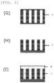
- the substrate used was a base substrate 7 (SiO 2 wafer substrate) having a dense line-and-space pattern shown in FIG. 2(G) (downward view) and (H) (cross-sectional view).
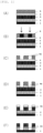
- the cross-sectional shape of each of the obtained wafer substrates was observed using an electron microscope (S-4700: manufactured by Hitachi, Ltd.), and the presence/absence of voids (gaps) inside the resist underlayer film filling the space between the lines was confirmed.
- Table 4 shows the results. In this evaluation, when a composition for forming a resist underlayer film having a poor filling property is used, voids are generated inside the resist underlayer film filling the space between the lines.
- Example Composition for forming resist underlayer film Heating temperature when forming resist underlayer film Oxygen concentration Filling property Volume % Voids
- Example 1-1 UDL-1 500°C 0.01 Absent
- Example 1-2 UDL-2 500°C 0.01 Absent
- Example 1-3 UDL-3 500°C 0.01 Absent
- Example 1-4 UDL-4 500°C 0.01 Absent
- Example 1-5 UDL-5 500°C 0.01 Absent
- Example 1-6 UDL-6 500°C 0.01 Absent
- Example 1-7 UDL-7 500°C 0.01 Absent
- Example 1-9 UDL-9 500°C 0.01 Absent
- Example 1-10 UDL-10 500°C 0.01 Absent
- Example 1-11 UDL-11 500°C 0.01 Absent
- Example 1-12 UDL-12 500°C 0.01 Absent
- Example 1-13 UDL-13 500°C 0.01 Absent
- Example 1-14 UDL-14 500°C 0.01 Absent
- Example 1-15 UDL-15 500°C 0.01 Abs
- Comparative Example 1-2 where the resist underlayer film was formed by heating under an air atmosphere at 500°C for 60 seconds, voids were observed at the bottom of the pattern. Even when the composition UDL-1 for forming a resist underlayer film, containing the compound (A-1) for forming a resist underlayer film, the compound having an organic crosslinking group, is used, volume shrinkage due to high-temperature baking in an air atmosphere is great. Therefore, this case can be said to be unfavorable from the viewpoint of filling property.
- compositions (UDL-1 to -20 and comparative UDL-1) for forming a resist underlayer film were respectively applied onto a silicon substrate and heated by using a hot plate at 350°C for 60 seconds to form a resist underlayer film having a film thickness of 80 nm (film thickness "a").
- a substrate coated with the composition and heated at 350°C for 60 seconds was further heated at 500°C for 60 seconds under a nitrogen atmosphere (oxygen concentration: 0.01 volume %) to form a resist underlayer film having a film thickness of 80 nm (film thickness "a”).
- etching was performed with CF 4 gas under the following conditions by using an etching apparatus CE-300I manufactured by ULVAC, Inc., and the film thickness "b" was measured. Then, the film thickness etched in 1 minute was calculated as an etching rate (nm/min) from the film thickness etched (film thickness "a” - film thickness "b") using each gas in a specified time. Table 5 shows the results.
- compositions (UDL-1 to -17 and comparative UDL-1) for forming a resist underlayer film were respectively applied onto an SiO 2 wafer substrate, baked in the atmosphere at 350°C for 60 seconds, and then baked at an oxygen concentration of 0.01 volume % at 500°C for 60 seconds to form a resist underlayer film having a thickness of 80 nm.
- a silicon-containing resist middle layer film material (SOG-1) was applied thereto, followed by baking at 220°C for 60 seconds to form a resist middle layer film having a thickness of 50 nm.
- a monolayer resist for ArF as a resist upper layer film material was applied thereto, followed by baking at 105°C for 60 seconds to form a photoresist film having a thickness of 100 nm.
- a liquid immersion top coat composition (TC-1) was applied to the photoresist film, followed by baking at 90°C for 60 seconds to form a top coat having a thickness of 50 nm.
- the silicon-containing resist middle layer film material was prepared by dissolving a polymer represented by an ArF silicon-containing middle layer film polymer (SiP1) and a thermal crosslinking catalyst (CAT1) in an organic solvent containing 0.1 mass% of FC-4430 (manufactured by Sumitomo 3M Limited) in the proportion shown in Table 6; and filtering the solution through a filter made of a fluororesin and having a pore size of 0.1 ⁇ m.
- Polymer Thermal crosslinking catalyst Organic solvent parts by mass
- SOG-1 SiP1 (100)
- CAT1 Propylene glycol monoethyl ether
- the resist upper layer film material (monolayer resist for ArF) was prepared by dissolving a polymer (RP1), an acid generator (PAG1), and a basic compound (Amine1), each in the proportion shown in Table 7, in a solvent containing 0.1% by mass of a surfactant (FC-4430: manufactured by Sumitomo 3M Limited), and filtering the solution through a 0.1-pm filter made of a fluororesin.
- RP1 polymer
- PAG1 acid generator
- Amine1 basic compound
- FC-4430 manufactured by Sumitomo 3M Limited
- the polymer (RP1), the acid generator (PAG1), and the basic compound (Amine1) used for the resist upper layer film material (monolayer resist for ArF) are shown below.
- the liquid immersion top coat composition (TC-1) was prepared by dissolving a top coat polymer (PP1) in an organic solvent at the proportion shown in Table 8, and filtering the solution through a 0.1-pm filter made of a fluororesin.
- Top coat polymer parts by mass
- Organic solvent parts by mass
- TC-1 PP1 100
- Diisoamyl ether (2,700)
- 2-methyl-1-butanol 270
- the top coat polymer (PP1) used for the liquid immersion top coat composition (TC-1) is shown below.
- the substrate was exposed to light with an ArF liquid immersion exposure apparatus (NSR-S610C manufactured by Nikon Corporation, NA: 1.30, ⁇ : 0.98/0.65, 35° s-polarized dipole illumination, 6% halftone phase shift mask), baked at 100°C for 60 seconds (PEB), and developed with a 2.38% by mass aqueous solution of tetramethylammonium hydroxide (TMAH) for 30 seconds, thereby obtaining a 55 nm 1:1 positive line-and-space pattern (a resist upper layer film pattern).
- NSR-S610C ArF liquid immersion exposure apparatus
- NA NA: 1.30
- ⁇ 0.98/0.65, 35° s-polarized dipole illumination, 6% halftone phase shift mask
- the resist middle layer film was etched by dry etching while using the resist upper layer film pattern as a mask to form a hard mask pattern.
- a resist underlayer film was then etched while using the obtained hard mask pattern as a mask to form a resist underlayer film pattern, and the SiO 2 film was etched while using the obtained resist underlayer film pattern as a mask.
- the etching conditions were as follows.
- Table 9 shows the results obtained by observation of the pattern cross section with an electron microscope (S-4700) manufactured by Hitachi, Ltd.
- Example Composition for forming resist underlayer film Patterning process Pattern profile Example 3-1 UDL-1 Vertical profile Example 3-2 UDL-2 Vertical profile Example 3-3 UDL-3 Vertical profile Example 3-4 UDL-4 Vertical profile Example 3-5 UDL-5 Vertical profile Example 3-6 UDL-6 Vertical profile Example 3-7 UDL-7 Vertical profile Example 3-8 UDL-8 Vertical profile Example 3-9 UDL-9 Vertical profile Example 3-10 UDL-10 Vertical profile Example 3-11 UDL-11 Vertical profile Example 3-12 UDL-12 Vertical profile Example 3-13 UDL-13 Vertical profile Example 3-14 UDL-14 Vertical profile Example 3-15 UDL-15 Vertical profile Example 3-16 UDL-16 Vertical profile Example 3-17 UDL-17 Vertical profile Comparative Example 3-1 Distorted pattern
- inventive methods for forming a resist underlayer film and patterning processes are particularly suitably employed in a multilayer resist process including the filling and planarization of a substrate to be processed having steps or unevenness, and are extremely useful in fine patterning for manufacturing semiconductor devices.
- the present description includes the following embodiments.
Landscapes
- Physics & Mathematics (AREA)
- General Physics & Mathematics (AREA)
- Engineering & Computer Science (AREA)
- Chemical & Material Sciences (AREA)
- Architecture (AREA)
- Structural Engineering (AREA)
- Organic Chemistry (AREA)
- Spectroscopy & Molecular Physics (AREA)
- Materials Engineering (AREA)
- Wood Science & Technology (AREA)
- Life Sciences & Earth Sciences (AREA)
- Photosensitive Polymer And Photoresist Processing (AREA)
- Exposure Of Semiconductors, Excluding Electron Or Ion Beam Exposure (AREA)
- Materials For Photolithography (AREA)
Applications Claiming Priority (2)
| Application Number | Priority Date | Filing Date | Title |
|---|---|---|---|
| JP2023038307 | 2023-03-13 | ||
| JP2023204015A JP2024129784A (ja) | 2023-03-13 | 2023-12-01 | レジスト下層膜形成方法、パターン形成方法 |
Publications (1)
| Publication Number | Publication Date |
|---|---|
| EP4432011A1 true EP4432011A1 (de) | 2024-09-18 |
Family
ID=90363228
Family Applications (1)
| Application Number | Title | Priority Date | Filing Date |
|---|---|---|---|
| EP24162134.1A Pending EP4432011A1 (de) | 2023-03-13 | 2024-03-07 | Verfahren zur bildung eines resistunterschichtfilms und strukturierungsverfahren |
Country Status (5)
| Country | Link |
|---|---|
| US (1) | US20240310732A1 (de) |
| EP (1) | EP4432011A1 (de) |
| KR (1) | KR102828276B1 (de) |
| IL (1) | IL311277A (de) |
| TW (1) | TWI885785B (de) |
Cited By (2)
| Publication number | Priority date | Publication date | Assignee | Title |
|---|---|---|---|---|
| EP4474524A3 (de) * | 2023-06-07 | 2025-03-12 | Shin-Etsu Chemical Co., Ltd. | Verbindung zur bildung eines metallhaltigen films, zusammensetzung zur bildung eines metallhaltigen films, verfahren zur herstellung einer verbindung und strukturierungsverfahren |
| EP4589383A3 (de) * | 2024-01-17 | 2025-10-08 | Shin-Etsu Chemical Co., Ltd. | Verbindung zur bildung eines metallhaltigen films, zusammensetzung zur bildung eines metallhaltigen films und strukturierungsverfahren |
Citations (18)
| Publication number | Priority date | Publication date | Assignee | Title |
|---|---|---|---|---|
| JP2002334869A (ja) | 2001-02-07 | 2002-11-22 | Tokyo Electron Ltd | シリコン窒化膜の形成方法、形成装置及びこの形成装置の洗浄前処理方法 |
| JP2004153125A (ja) | 2002-10-31 | 2004-05-27 | Fujitsu Ltd | 加工用マスクの形成方法及び半導体装置の製造方法 |
| JP2004205685A (ja) | 2002-12-24 | 2004-07-22 | Shin Etsu Chem Co Ltd | パターン形成方法及び下層膜形成材料 |
| WO2004066377A1 (ja) | 2003-01-24 | 2004-08-05 | Tokyo Electron Limited | 被処理基板上にシリコン窒化膜を形成するcvd方法 |
| JP2005128509A (ja) | 2003-10-03 | 2005-05-19 | Shin Etsu Chem Co Ltd | フォトレジスト下層膜形成材料及びパターン形成方法 |
| JP2007199653A (ja) | 2005-12-27 | 2007-08-09 | Shin Etsu Chem Co Ltd | フォトレジスト下層膜形成材料及びパターン形成方法 |
| JP2009269953A (ja) | 2008-05-01 | 2009-11-19 | Shin Etsu Chem Co Ltd | 新規光酸発生剤並びにこれを用いたレジスト材料及びパターン形成方法 |
| US20150099228A1 (en) * | 2013-10-04 | 2015-04-09 | Shin-Etsu Chemical Co., Ltd. | Resist composition and patterning process |
| US20160314984A1 (en) * | 2015-04-24 | 2016-10-27 | Jsr Corporation | Method for film formation, and pattern-forming method |
| JP6189758B2 (ja) | 2013-03-15 | 2017-08-30 | 信越化学工業株式会社 | チタン含有レジスト下層膜形成用組成物及びパターン形成方法 |
| JP6714493B2 (ja) | 2015-12-24 | 2020-06-24 | 信越化学工業株式会社 | 有機膜形成用化合物、有機膜形成用組成物、有機膜形成方法、及びパターン形成方法 |
| JP6786391B2 (ja) | 2013-08-30 | 2020-11-18 | メルク パテント ゲゼルシャフト ミット ベシュレンクテル ハフツングMerck Patent Gesellschaft mit beschraenkter Haftung | ハードマスクおよび充填材料として安定な金属化合物、その組成物、およびその使用方法 |
| WO2021209476A1 (en) * | 2020-04-17 | 2021-10-21 | Merck Patent Gmbh | A spin coating composition comprising a carbon material, a metal organic compound, and solvent, and a manufacturing method of a metal oxide film above a substrate |
| EP4339702A1 (de) * | 2022-09-14 | 2024-03-20 | Shin-Etsu Chemical Co., Ltd. | Verbindung zur bildung eines metallhaltigen films, zusammensetzung zur bildung eines metallhaltigen films, strukturierungsverfahren und halbleiterfotoresistmaterial |
| EP4369100A1 (de) * | 2022-11-08 | 2024-05-15 | Shin-Etsu Chemical Co., Ltd. | Verbindung zur bildung eines metallhaltigen films, zusammensetzung zur bildung eines metallhaltigen films und strukturierungsverfahren |
| EP4390548A1 (de) * | 2022-12-22 | 2024-06-26 | Shin-Etsu Chemical Co., Ltd. | Verbindung zur bildung eines metallhaltigen films, zusammensetzung zur bildung eines metallhaltigen films und strukturierungsverfahren |
| EP4398036A1 (de) * | 2023-01-06 | 2024-07-10 | Shin-Etsu Chemical Co., Ltd. | Verbindung zur bildung eines metallhaltigen films, zusammensetzung zur bildung eines metallhaltigen films und strukturierungsverfahren |
| EP4398037A1 (de) * | 2023-01-06 | 2024-07-10 | Shin-Etsu Chemical Co., Ltd. | Verbindung zur bildung eines metallhaltigen films, zusammensetzung zur bildung eines metallhaltigen films und strukturierungsverfahren |
Family Cites Families (2)
| Publication number | Priority date | Publication date | Assignee | Title |
|---|---|---|---|---|
| JP5365809B2 (ja) * | 2008-02-18 | 2013-12-11 | 日産化学工業株式会社 | 環状アミノ基を有するシリコン含有レジスト下層膜形成組成物 |
| JP7611785B2 (ja) * | 2021-07-06 | 2025-01-10 | 信越化学工業株式会社 | 密着膜形成材料、これを用いた密着膜の形成方法、及び密着膜形成材料を用いたパターン形成方法 |
-
2024
- 2024-03-05 IL IL311277A patent/IL311277A/en unknown
- 2024-03-07 EP EP24162134.1A patent/EP4432011A1/de active Pending
- 2024-03-08 TW TW113108550A patent/TWI885785B/zh active
- 2024-03-11 KR KR1020240034011A patent/KR102828276B1/ko active Active
- 2024-03-11 US US18/601,541 patent/US20240310732A1/en active Pending
Patent Citations (20)
| Publication number | Priority date | Publication date | Assignee | Title |
|---|---|---|---|---|
| JP2002334869A (ja) | 2001-02-07 | 2002-11-22 | Tokyo Electron Ltd | シリコン窒化膜の形成方法、形成装置及びこの形成装置の洗浄前処理方法 |
| JP2004153125A (ja) | 2002-10-31 | 2004-05-27 | Fujitsu Ltd | 加工用マスクの形成方法及び半導体装置の製造方法 |
| JP2004205685A (ja) | 2002-12-24 | 2004-07-22 | Shin Etsu Chem Co Ltd | パターン形成方法及び下層膜形成材料 |
| WO2004066377A1 (ja) | 2003-01-24 | 2004-08-05 | Tokyo Electron Limited | 被処理基板上にシリコン窒化膜を形成するcvd方法 |
| JP2005128509A (ja) | 2003-10-03 | 2005-05-19 | Shin Etsu Chem Co Ltd | フォトレジスト下層膜形成材料及びパターン形成方法 |
| JP2007199653A (ja) | 2005-12-27 | 2007-08-09 | Shin Etsu Chem Co Ltd | フォトレジスト下層膜形成材料及びパターン形成方法 |
| JP2009269953A (ja) | 2008-05-01 | 2009-11-19 | Shin Etsu Chem Co Ltd | 新規光酸発生剤並びにこれを用いたレジスト材料及びパターン形成方法 |
| JP6189758B2 (ja) | 2013-03-15 | 2017-08-30 | 信越化学工業株式会社 | チタン含有レジスト下層膜形成用組成物及びパターン形成方法 |
| JP6786391B2 (ja) | 2013-08-30 | 2020-11-18 | メルク パテント ゲゼルシャフト ミット ベシュレンクテル ハフツングMerck Patent Gesellschaft mit beschraenkter Haftung | ハードマスクおよび充填材料として安定な金属化合物、その組成物、およびその使用方法 |
| JP7050137B2 (ja) | 2013-08-30 | 2022-04-07 | メルク パテント ゲゼルシャフト ミット ベシュレンクテル ハフツング | ハードマスクおよび充填材料として安定な金属化合物、その組成物、およびその使用方法 |
| US20150099228A1 (en) * | 2013-10-04 | 2015-04-09 | Shin-Etsu Chemical Co., Ltd. | Resist composition and patterning process |
| JP6711104B2 (ja) | 2015-04-24 | 2020-06-17 | Jsr株式会社 | レジスト下層膜形成方法及びパターン形成方法 |
| US20160314984A1 (en) * | 2015-04-24 | 2016-10-27 | Jsr Corporation | Method for film formation, and pattern-forming method |
| JP6714493B2 (ja) | 2015-12-24 | 2020-06-24 | 信越化学工業株式会社 | 有機膜形成用化合物、有機膜形成用組成物、有機膜形成方法、及びパターン形成方法 |
| WO2021209476A1 (en) * | 2020-04-17 | 2021-10-21 | Merck Patent Gmbh | A spin coating composition comprising a carbon material, a metal organic compound, and solvent, and a manufacturing method of a metal oxide film above a substrate |
| EP4339702A1 (de) * | 2022-09-14 | 2024-03-20 | Shin-Etsu Chemical Co., Ltd. | Verbindung zur bildung eines metallhaltigen films, zusammensetzung zur bildung eines metallhaltigen films, strukturierungsverfahren und halbleiterfotoresistmaterial |
| EP4369100A1 (de) * | 2022-11-08 | 2024-05-15 | Shin-Etsu Chemical Co., Ltd. | Verbindung zur bildung eines metallhaltigen films, zusammensetzung zur bildung eines metallhaltigen films und strukturierungsverfahren |
| EP4390548A1 (de) * | 2022-12-22 | 2024-06-26 | Shin-Etsu Chemical Co., Ltd. | Verbindung zur bildung eines metallhaltigen films, zusammensetzung zur bildung eines metallhaltigen films und strukturierungsverfahren |
| EP4398036A1 (de) * | 2023-01-06 | 2024-07-10 | Shin-Etsu Chemical Co., Ltd. | Verbindung zur bildung eines metallhaltigen films, zusammensetzung zur bildung eines metallhaltigen films und strukturierungsverfahren |
| EP4398037A1 (de) * | 2023-01-06 | 2024-07-10 | Shin-Etsu Chemical Co., Ltd. | Verbindung zur bildung eines metallhaltigen films, zusammensetzung zur bildung eines metallhaltigen films und strukturierungsverfahren |
Cited By (2)
| Publication number | Priority date | Publication date | Assignee | Title |
|---|---|---|---|---|
| EP4474524A3 (de) * | 2023-06-07 | 2025-03-12 | Shin-Etsu Chemical Co., Ltd. | Verbindung zur bildung eines metallhaltigen films, zusammensetzung zur bildung eines metallhaltigen films, verfahren zur herstellung einer verbindung und strukturierungsverfahren |
| EP4589383A3 (de) * | 2024-01-17 | 2025-10-08 | Shin-Etsu Chemical Co., Ltd. | Verbindung zur bildung eines metallhaltigen films, zusammensetzung zur bildung eines metallhaltigen films und strukturierungsverfahren |
Also Published As
| Publication number | Publication date |
|---|---|
| US20240310732A1 (en) | 2024-09-19 |
| KR102828276B1 (ko) | 2025-07-01 |
| KR20240139010A (ko) | 2024-09-20 |
| IL311277A (en) | 2024-10-01 |
| TW202442656A (zh) | 2024-11-01 |
| TWI885785B (zh) | 2025-06-01 |
Similar Documents
| Publication | Publication Date | Title |
|---|---|---|
| EP4369100A1 (de) | Verbindung zur bildung eines metallhaltigen films, zusammensetzung zur bildung eines metallhaltigen films und strukturierungsverfahren | |
| EP4432011A1 (de) | Verfahren zur bildung eines resistunterschichtfilms und strukturierungsverfahren | |
| EP4398036A1 (de) | Verbindung zur bildung eines metallhaltigen films, zusammensetzung zur bildung eines metallhaltigen films und strukturierungsverfahren | |
| EP4390548A1 (de) | Verbindung zur bildung eines metallhaltigen films, zusammensetzung zur bildung eines metallhaltigen films und strukturierungsverfahren | |
| EP4435516A1 (de) | Verfahren zur bildung eines resistunterschichtfilms und strukturierungsverfahren | |
| EP4425260A1 (de) | Verbindung zur bildung eines metallhaltigen films, zusammensetzung zur bildung eines metallhaltigen films und strukturierungsverfahren | |
| EP4474524A2 (de) | Verbindung zur bildung eines metallhaltigen films, zusammensetzung zur bildung eines metallhaltigen films, verfahren zur herstellung einer verbindung und strukturierungsverfahren | |
| JP2024129784A (ja) | レジスト下層膜形成方法、パターン形成方法 | |
| TWI916841B (zh) | 含金屬之膜形成用化合物、含金屬之膜形成用組成物、含金屬之膜形成用化合物之製造方法、及圖案形成方法 | |
| EP4589383A2 (de) | Verbindung zur bildung eines metallhaltigen films, zusammensetzung zur bildung eines metallhaltigen films und strukturierungsverfahren | |
| EP4592753A2 (de) | Zusammensetzung zur bildung eines metallhaltigen films und strukturierungsverfahren | |
| JP2024132848A (ja) | レジスト下層膜形成方法、及びパターン形成方法 | |
| CN118642329A (zh) | 抗蚀剂下层膜形成方法、图案形成方法 |
Legal Events
| Date | Code | Title | Description |
|---|---|---|---|
| PUAI | Public reference made under article 153(3) epc to a published international application that has entered the european phase |
Free format text: ORIGINAL CODE: 0009012 |
|
| STAA | Information on the status of an ep patent application or granted ep patent |
Free format text: STATUS: THE APPLICATION HAS BEEN PUBLISHED |
|
| AK | Designated contracting states |
Kind code of ref document: A1 Designated state(s): AL AT BE BG CH CY CZ DE DK EE ES FI FR GB GR HR HU IE IS IT LI LT LU LV MC ME MK MT NL NO PL PT RO RS SE SI SK SM TR |
|
| STAA | Information on the status of an ep patent application or granted ep patent |
Free format text: STATUS: REQUEST FOR EXAMINATION WAS MADE |
|
| 17P | Request for examination filed |
Effective date: 20241125 |
|
| RBV | Designated contracting states (corrected) |
Designated state(s): AL AT BE BG CH CY CZ DE DK EE ES FI FR GB GR HR HU IE IS IT LI LT LU LV MC ME MK MT NL NO PL PT RO RS SE SI SK SM TR |