EP4428932A2 - Solarzelle und herstellungsverfahren dafür, photovoltaisches modul, und photovoltaiches system - Google Patents
Solarzelle und herstellungsverfahren dafür, photovoltaisches modul, und photovoltaiches system Download PDFInfo
- Publication number
- EP4428932A2 EP4428932A2 EP24191111.4A EP24191111A EP4428932A2 EP 4428932 A2 EP4428932 A2 EP 4428932A2 EP 24191111 A EP24191111 A EP 24191111A EP 4428932 A2 EP4428932 A2 EP 4428932A2
- Authority
- EP
- European Patent Office
- Prior art keywords
- emitter
- sub
- region
- layer
- disposed
- Prior art date
- Legal status (The legal status is an assumption and is not a legal conclusion. Google has not performed a legal analysis and makes no representation as to the accuracy of the status listed.)
- Pending
Links
- 238000002360 preparation method Methods 0.000 title description 15
- 239000000758 substrate Substances 0.000 claims abstract description 81
- 230000005641 tunneling Effects 0.000 claims description 52
- 238000000034 method Methods 0.000 claims description 27
- 238000002161 passivation Methods 0.000 claims description 25
- VYPSYNLAJGMNEJ-UHFFFAOYSA-N Silicium dioxide Chemical compound O=[Si]=O VYPSYNLAJGMNEJ-UHFFFAOYSA-N 0.000 claims description 21
- 229910052814 silicon oxide Inorganic materials 0.000 claims description 21
- IJGRMHOSHXDMSA-UHFFFAOYSA-N Atomic nitrogen Chemical compound N#N IJGRMHOSHXDMSA-UHFFFAOYSA-N 0.000 claims description 18
- OKTJSMMVPCPJKN-UHFFFAOYSA-N Carbon Chemical compound [C] OKTJSMMVPCPJKN-UHFFFAOYSA-N 0.000 claims description 9
- QVGXLLKOCUKJST-UHFFFAOYSA-N atomic oxygen Chemical compound [O] QVGXLLKOCUKJST-UHFFFAOYSA-N 0.000 claims description 9
- 229910052799 carbon Inorganic materials 0.000 claims description 9
- 229910052757 nitrogen Inorganic materials 0.000 claims description 9
- 229910052760 oxygen Inorganic materials 0.000 claims description 9
- 239000001301 oxygen Substances 0.000 claims description 9
- 239000000463 material Substances 0.000 description 54
- 238000010438 heat treatment Methods 0.000 description 16
- 239000003989 dielectric material Substances 0.000 description 15
- ZOXJGFHDIHLPTG-UHFFFAOYSA-N Boron Chemical compound [B] ZOXJGFHDIHLPTG-UHFFFAOYSA-N 0.000 description 14
- OAICVXFJPJFONN-UHFFFAOYSA-N Phosphorus Chemical compound [P] OAICVXFJPJFONN-UHFFFAOYSA-N 0.000 description 14
- 229910052796 boron Inorganic materials 0.000 description 14
- 229910052698 phosphorus Inorganic materials 0.000 description 14
- 239000011574 phosphorus Substances 0.000 description 14
- 239000002019 doping agent Substances 0.000 description 8
- 230000002708 enhancing effect Effects 0.000 description 8
- 230000001965 increasing effect Effects 0.000 description 7
- 230000003647 oxidation Effects 0.000 description 7
- 238000007254 oxidation reaction Methods 0.000 description 7
- 238000005538 encapsulation Methods 0.000 description 6
- 230000009286 beneficial effect Effects 0.000 description 5
- 230000000694 effects Effects 0.000 description 5
- 238000000623 plasma-assisted chemical vapour deposition Methods 0.000 description 5
- 229910052581 Si3N4 Inorganic materials 0.000 description 4
- 229910021417 amorphous silicon Inorganic materials 0.000 description 4
- 238000003491 array Methods 0.000 description 4
- 238000009792 diffusion process Methods 0.000 description 4
- 229910021424 microcrystalline silicon Inorganic materials 0.000 description 4
- 239000000203 mixture Substances 0.000 description 4
- HQVNEWCFYHHQES-UHFFFAOYSA-N silicon nitride Chemical compound N12[Si]34N5[Si]62N3[Si]51N64 HQVNEWCFYHHQES-UHFFFAOYSA-N 0.000 description 4
- 238000004518 low pressure chemical vapour deposition Methods 0.000 description 3
- 229910021420 polycrystalline silicon Inorganic materials 0.000 description 3
- 229920005591 polysilicon Polymers 0.000 description 3
- GWEVSGVZZGPLCZ-UHFFFAOYSA-N Titan oxide Chemical compound O=[Ti]=O GWEVSGVZZGPLCZ-UHFFFAOYSA-N 0.000 description 2
- 230000015572 biosynthetic process Effects 0.000 description 2
- 239000006227 byproduct Substances 0.000 description 2
- 238000004140 cleaning Methods 0.000 description 2
- 230000005611 electricity Effects 0.000 description 2
- 238000005516 engineering process Methods 0.000 description 2
- 238000010329 laser etching Methods 0.000 description 2
- ORUIBWPALBXDOA-UHFFFAOYSA-L magnesium fluoride Chemical compound [F-].[F-].[Mg+2] ORUIBWPALBXDOA-UHFFFAOYSA-L 0.000 description 2
- 229910001635 magnesium fluoride Inorganic materials 0.000 description 2
- 238000004519 manufacturing process Methods 0.000 description 2
- TWNQGVIAIRXVLR-UHFFFAOYSA-N oxo(oxoalumanyloxy)alumane Chemical compound O=[Al]O[Al]=O TWNQGVIAIRXVLR-UHFFFAOYSA-N 0.000 description 2
- 239000004065 semiconductor Substances 0.000 description 2
- 239000002210 silicon-based material Substances 0.000 description 2
- 239000000243 solution Substances 0.000 description 2
- OGIDPMRJRNCKJF-UHFFFAOYSA-N titanium oxide Inorganic materials [Ti]=O OGIDPMRJRNCKJF-UHFFFAOYSA-N 0.000 description 2
- 238000003466 welding Methods 0.000 description 2
- 238000001039 wet etching Methods 0.000 description 2
- XUIMIQQOPSSXEZ-UHFFFAOYSA-N Silicon Chemical compound [Si] XUIMIQQOPSSXEZ-UHFFFAOYSA-N 0.000 description 1
- 230000004931 aggregating effect Effects 0.000 description 1
- 239000012670 alkaline solution Substances 0.000 description 1
- 230000005540 biological transmission Effects 0.000 description 1
- 238000006243 chemical reaction Methods 0.000 description 1
- 239000000356 contaminant Substances 0.000 description 1
- 238000000151 deposition Methods 0.000 description 1
- 229920001971 elastomer Polymers 0.000 description 1
- 239000000806 elastomer Substances 0.000 description 1
- 239000005038 ethylene vinyl acetate Substances 0.000 description 1
- 239000011521 glass Substances 0.000 description 1
- 238000002955 isolation Methods 0.000 description 1
- 229910052751 metal Inorganic materials 0.000 description 1
- 239000002184 metal Substances 0.000 description 1
- 238000012986 modification Methods 0.000 description 1
- 230000004048 modification Effects 0.000 description 1
- 229920003023 plastic Polymers 0.000 description 1
- 239000004033 plastic Substances 0.000 description 1
- 229920001200 poly(ethylene-vinyl acetate) Polymers 0.000 description 1
- -1 polyethylene terephthalate Polymers 0.000 description 1
- 229920000139 polyethylene terephthalate Polymers 0.000 description 1
- 239000005020 polyethylene terephthalate Substances 0.000 description 1
- 238000010248 power generation Methods 0.000 description 1
- 230000005855 radiation Effects 0.000 description 1
- 230000006798 recombination Effects 0.000 description 1
- 238000005215 recombination Methods 0.000 description 1
- 229910052710 silicon Inorganic materials 0.000 description 1
- 239000010703 silicon Substances 0.000 description 1
- 238000005245 sintering Methods 0.000 description 1
- XLYOFNOQVPJJNP-UHFFFAOYSA-N water Substances O XLYOFNOQVPJJNP-UHFFFAOYSA-N 0.000 description 1
Images
Classifications
-
- H—ELECTRICITY
- H10—SEMICONDUCTOR DEVICES; ELECTRIC SOLID-STATE DEVICES NOT OTHERWISE PROVIDED FOR
- H10F—INORGANIC SEMICONDUCTOR DEVICES SENSITIVE TO INFRARED RADIATION, LIGHT, ELECTROMAGNETIC RADIATION OF SHORTER WAVELENGTH OR CORPUSCULAR RADIATION
- H10F77/00—Constructional details of devices covered by this subclass
- H10F77/10—Semiconductor bodies
- H10F77/14—Shape of semiconductor bodies; Shapes, relative sizes or dispositions of semiconductor regions within semiconductor bodies
- H10F77/147—Shapes of bodies
-
- H—ELECTRICITY
- H10—SEMICONDUCTOR DEVICES; ELECTRIC SOLID-STATE DEVICES NOT OTHERWISE PROVIDED FOR
- H10F—INORGANIC SEMICONDUCTOR DEVICES SENSITIVE TO INFRARED RADIATION, LIGHT, ELECTROMAGNETIC RADIATION OF SHORTER WAVELENGTH OR CORPUSCULAR RADIATION
- H10F10/00—Individual photovoltaic cells, e.g. solar cells
- H10F10/10—Individual photovoltaic cells, e.g. solar cells having potential barriers
- H10F10/14—Photovoltaic cells having only PN homojunction potential barriers
- H10F10/148—Double-emitter photovoltaic cells, e.g. bifacial photovoltaic cells
-
- H—ELECTRICITY
- H10—SEMICONDUCTOR DEVICES; ELECTRIC SOLID-STATE DEVICES NOT OTHERWISE PROVIDED FOR
- H10F—INORGANIC SEMICONDUCTOR DEVICES SENSITIVE TO INFRARED RADIATION, LIGHT, ELECTROMAGNETIC RADIATION OF SHORTER WAVELENGTH OR CORPUSCULAR RADIATION
- H10F10/00—Individual photovoltaic cells, e.g. solar cells
- H10F10/10—Individual photovoltaic cells, e.g. solar cells having potential barriers
- H10F10/14—Photovoltaic cells having only PN homojunction potential barriers
- H10F10/146—Back-junction photovoltaic cells, e.g. having interdigitated base-emitter regions on the back side
-
- H—ELECTRICITY
- H10—SEMICONDUCTOR DEVICES; ELECTRIC SOLID-STATE DEVICES NOT OTHERWISE PROVIDED FOR
- H10F—INORGANIC SEMICONDUCTOR DEVICES SENSITIVE TO INFRARED RADIATION, LIGHT, ELECTROMAGNETIC RADIATION OF SHORTER WAVELENGTH OR CORPUSCULAR RADIATION
- H10F10/00—Individual photovoltaic cells, e.g. solar cells
- H10F10/10—Individual photovoltaic cells, e.g. solar cells having potential barriers
- H10F10/16—Photovoltaic cells having only PN heterojunction potential barriers
- H10F10/164—Photovoltaic cells having only PN heterojunction potential barriers comprising heterojunctions with Group IV materials, e.g. ITO/Si or GaAs/SiGe photovoltaic cells
- H10F10/165—Photovoltaic cells having only PN heterojunction potential barriers comprising heterojunctions with Group IV materials, e.g. ITO/Si or GaAs/SiGe photovoltaic cells the heterojunctions being Group IV-IV heterojunctions, e.g. Si/Ge, SiGe/Si or Si/SiC photovoltaic cells
- H10F10/166—Photovoltaic cells having only PN heterojunction potential barriers comprising heterojunctions with Group IV materials, e.g. ITO/Si or GaAs/SiGe photovoltaic cells the heterojunctions being Group IV-IV heterojunctions, e.g. Si/Ge, SiGe/Si or Si/SiC photovoltaic cells the Group IV-IV heterojunctions being heterojunctions of crystalline and amorphous materials, e.g. silicon heterojunction [SHJ] photovoltaic cells
-
- H—ELECTRICITY
- H10—SEMICONDUCTOR DEVICES; ELECTRIC SOLID-STATE DEVICES NOT OTHERWISE PROVIDED FOR
- H10F—INORGANIC SEMICONDUCTOR DEVICES SENSITIVE TO INFRARED RADIATION, LIGHT, ELECTROMAGNETIC RADIATION OF SHORTER WAVELENGTH OR CORPUSCULAR RADIATION
- H10F71/00—Manufacture or treatment of devices covered by this subclass
- H10F71/121—The active layers comprising only Group IV materials
-
- H—ELECTRICITY
- H10—SEMICONDUCTOR DEVICES; ELECTRIC SOLID-STATE DEVICES NOT OTHERWISE PROVIDED FOR
- H10F—INORGANIC SEMICONDUCTOR DEVICES SENSITIVE TO INFRARED RADIATION, LIGHT, ELECTROMAGNETIC RADIATION OF SHORTER WAVELENGTH OR CORPUSCULAR RADIATION
- H10F77/00—Constructional details of devices covered by this subclass
- H10F77/10—Semiconductor bodies
- H10F77/14—Shape of semiconductor bodies; Shapes, relative sizes or dispositions of semiconductor regions within semiconductor bodies
-
- H—ELECTRICITY
- H10—SEMICONDUCTOR DEVICES; ELECTRIC SOLID-STATE DEVICES NOT OTHERWISE PROVIDED FOR
- H10F—INORGANIC SEMICONDUCTOR DEVICES SENSITIVE TO INFRARED RADIATION, LIGHT, ELECTROMAGNETIC RADIATION OF SHORTER WAVELENGTH OR CORPUSCULAR RADIATION
- H10F77/00—Constructional details of devices covered by this subclass
- H10F77/20—Electrodes
- H10F77/206—Electrodes for devices having potential barriers
- H10F77/211—Electrodes for devices having potential barriers for photovoltaic cells
- H10F77/219—Arrangements for electrodes of back-contact photovoltaic cells
- H10F77/227—Arrangements for electrodes of back-contact photovoltaic cells for emitter wrap-through [EWT] photovoltaic cells, e.g. interdigitated emitter-base back-contacts
-
- H—ELECTRICITY
- H10—SEMICONDUCTOR DEVICES; ELECTRIC SOLID-STATE DEVICES NOT OTHERWISE PROVIDED FOR
- H10F—INORGANIC SEMICONDUCTOR DEVICES SENSITIVE TO INFRARED RADIATION, LIGHT, ELECTROMAGNETIC RADIATION OF SHORTER WAVELENGTH OR CORPUSCULAR RADIATION
- H10F77/00—Constructional details of devices covered by this subclass
- H10F77/30—Coatings
- H10F77/306—Coatings for devices having potential barriers
- H10F77/311—Coatings for devices having potential barriers for photovoltaic cells
- H10F77/315—Coatings for devices having potential barriers for photovoltaic cells the coatings being antireflective or having enhancing optical properties
Definitions
- the present application relates to the field of solar cell technology, specifically to solar cells and preparation methods thereof, photovoltaic modules, and photovoltaic systems.
- Solar cells are devices that directly convert light energy into electrical energy through the photovoltaic effect. Solar cells are commonly prepared on semiconductor chips or substrates by using semiconductor processing technology to form a p-n junction adjacent to a surface of the substrate.
- IBC interdigitated back contact
- p-n junctions are located on the back side of the substrate, with p-doped and n-doped areas alternately arranged along the surface of the substrate.
- Solar radiation that irradiates the front side of the substrate enters the substrate and induces generation of electron-hole pairs within the substrate.
- These electron-hole pairs migrate to the p-doped and n-doped areas on the back side of the substrate, thereby generating a voltage difference between the doped areas.
- the doped areas are electrically connected to an external circuit through metal electrodes, thereby conducting electric currents from the solar cell to the external circuit.
- a first aspect of the present application provides a solar cell, including a semiconducting substrate, a first emitter, an insulating layer, and a second emitter.
- the semiconducting substrate includes a first surface and a second surface that are opposite to each other, the semiconducting substrate includes a first region and a second region that are arranged adjacent to each other in a first direction, the first region includes a first sub-region and a second sub-region that are arranged adjacent to each other in the first direction, the first sub-region is in contact with the second region, and the first direction is perpendicular to the thickness direction of the semiconducting substrate.
- the first emitter is disposed on the first surface and located on the first region.
- the insulating layer is disposed on the first emitter and located on the first sub-region.
- the second emitter is disposed on the first surface, the second emitter includes a first sub-emitter and a second sub-emitter that are connected with each other, the first sub-emitter is located on the second region, the second sub-emitter is disposed on the insulating layer, and electrical conduction exists between the first emitter and the first sub-emitter.
- the first surface includes a first sub-surface located in the first region and a second sub-surface located in the second region.
- the minimum distance between the first sub-surface and the second surface is greater than the minimum distance between the second sub-surface and the second surface.
- the first emitter is disposed on the first sub-surface, and the first sub-emitter is disposed on the second sub-surface.
- an orthogonal projection of the first emitter on a first plane overlaps with an orthogonal projection of the first sub-emitter on the first plane, forming an overlapping area.
- the first emitter includes a sidewall adjacent to the second region. Electrical conduction exists between the sidewall and the first sub-emitter.
- the first plane is parallel to the thickness direction of the semiconducting substrate and perpendicular to the first direction.
- the solar cell further includes a first tunneling layer, disposed between the first emitter and the semiconducting substrate; and a second tunneling layer, disposed between the second emitter and the semiconducting substrate.
- a portion of the second tunneling layer is disposed on the sidewall of the first emitter that is adjacent to the second region and is disposed between the first emitter and the first sub-emitter.
- the second tunneling layer includes a first sub-tunneling layer, disposed on the second sub-surface; and a second sub-tunneling layer, disposed on the sidewall of the first emitter that is adjacent to the second region.
- the second sub-tunneling layer is located between the first emitter and the first sub-emitter.
- the first sub-tunneling layer is spaced apart from the second sub-tunneling layer.
- the first sub-emitter covers at least a surface of the first sub-tunneling layer away from the semiconducting substrate, a sidewall of the first tunneling layer adjacent to the second region, and a sidewall of the second sub-tunneling layer adjacent to the second region.
- one end of the second sub-tunneling layer is connected to the first sub-tunneling layer, while another end of the second sub-tunneling layer extends in a direction away from the semiconducting substrate.
- the second sub-tunneling layer covers at least a sidewall of the first tunneling layer adjacent to the second region, a sidewall of the first emitter adjacent to the second region, and a sidewall of the insulating layer adjacent to the second region.
- the second tunneling layer further includes a third sub-tunneling layer.
- the third sub-tunneling layer is connected to the second sub-tunneling layer, and is located between the insulating layer and the second sub-emitter.
- the solar cell further includes a first electrode and a second electrode.
- the first electrode is disposed on a side of the first emitter that is away from the semiconducting substrate, and electrically connected to the first emitter.
- the first electrode is spaced apart from the insulating layer.
- the second electrode is disposed on a side of the second emitter that is away from the semiconducting substrate, and electrically connected to the second emitter.
- a sidewall of the insulating layer adjacent to the first electrode is distanced from the center of the first emitter by a first distance along the first direction, the first distance ranges from 3 ⁇ m to 10000 ⁇ m.
- a size of the insulating layer along the first direction is defined as a first dimension, represented by W, which satisfies 0 ⁇ W ⁇ L;
- L is a distance between a sidewall of the first electrode adjacent to the insulating layer and a sidewall of the first emitter adjacent to the second region.
- a thickness of the first emitter is in a range from 5nm to 2500nm.
- a thickness of the second emitter is in a range from 5nm to 2500nm.
- the first emitter is doped with oxygen, nitrogen, carbon, or any combination thereof.
- the second emitter is doped with oxygen, nitrogen, carbon, or any combination thereof.
- the insulating layer is a silicon oxide dielectric layer.
- the solar cell further includes a first passivation layer, a first anti-reflection layer, a second passivation layer, and a second anti-reflection layer.
- the first passivation layer is disposed on a side of the first emitter and the second emitter that is away from the semiconducting substrate.
- the first anti-reflection layer is disposed on a side of the first passivation layer that is away from the semiconducting substrate.
- the second passivation layer is disposed on the second surface.
- the second anti-reflection layer is disposed on the side of the second passivation layer that is away from the semiconducting substrate.
- a second aspect of the present application provides a method for preparing a solar cell, including:
- the semiconducting substrate including a first surface and a second surface opposite to each other, the semiconducting substrate including a first region and a second region arranged adjacent to each other in a first direction, the first region including a first sub-region and a second sub-region arranged adjacent to each other in the first direction, the first sub-region being in contact with the second region, the first direction being perpendicular to the thickness direction of the semiconducting substrate;
- first emitter and a second emitter on the first surface, and forming an insulating layer on the first emitter and on the first sub-region; wherein the first emitter is formed on the first region, the second emitter includes a first sub-emitter and a second sub-emitter connected with each other, the first sub-emitter is formed on the second region, the second sub-emitter is formed on the insulating layer, electrical conduction is formed between the first emitter and the first sub-emitter.
- a third aspect of the present application provides a photovoltaic module, including the solar cell of any above embodiment.
- a fourth aspect of the present application provides a photovoltaic system, including the photovoltaic module in the third aspect.
- the insulating layer is disposed on the first emitter, the first sub-emitter of the second emitter is located on the second region, the second sub-emitter of the second emitter is disposed on the insulating layer, and electrical conduction is formed between the first emitter and the first sub-emitter so as to form a current leakage path.
- the current can flow through the current leakage path in this solar cell, thereby preventing the hotspot effect from occurring in the photovoltaic module, thus increasing the lifetime of the solar cell.
- the insulating layer is sandwiched between the first emitter and the second sub-emitter, the current leakage area between the first emitter and the second emitter can be reduced, thereby reducing the leakage current, which is conducive to enhancing the working efficiency of the solar cell.
- the insulating layer can also protect the first emitter, reducing damage to the first emitter during the preparation process, thus improving the structural integrity of the first emitter, which is thus beneficial for improving the performance of the solar cell.
- the spatial relation terms such as “below”, “under”, “beneath”, “above”, “on”, “over”, etc., may be used herein to describe the relationships of an element or a feature with other elements or features shown in the drawings. It should be understood that the terms of spatial relations are intended to include other different orientations in use or operation in addition to the orientation of the elements or features shown in the drawings. For example, if the drawings are placed upside down, the element or feature which was “above” or “over” other elements or features will be “below” or “under” other elements or features. Thus, the exemplary terms “below” and “beneath” may cover the meanings of “above” or “below”.
- the element or feature can also be positioned in other different ways (e.g., rotating 90 degrees or at other orientations), and the spatial relation terms used herein can be correspondingly interpreted.
- an element when mentioning that an element is "located on" a region of the semiconducting substrate, it means that this element is located corresponding to this region in the thickness direction of the semiconducting substrate, and that is, the projection of this element is located in the projection of this region on the plane perpendicular to the thickness direction of the semiconducting substrate.
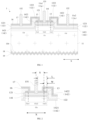
- an embodiment of a solar cell 1 includes a semiconducting substrate 11, a first emitter 121, an insulating layer 13, and a second emitter 122.
- the semiconducting substrate 11 includes a first surface 11a and a second surface 11b that are opposite to each other.
- the first surface 11a can be the back surface away from the sun
- the second surface 11b can be the front surface facing the sun.
- the semiconducting substrate 11 includes a first region 11c and a second region 11d that are arranged adjacent to each other in a first direction X.
- the first direction X is a direction perpendicular to the thickness direction of the semiconducting substrate 11.
- the first region 11c includes a first sub-region 11c1 and a second sub-region 11c2 that are arranged adjacent to each other in the first direction X.
- the first sub-region 11c1 is in contact with the second region 11d.
- the first emitter 121 is disposed on the first surface 11a and located on the first region 11c.
- the insulating layer 13 is disposed on the first emitter 121 and located on the first sub-region 11c1.
- the second emitter 122 is disposed on the first surface 11a.
- the second emitter 122 includes a first sub-emitter 1221 and a second sub-emitter 1222, and the first and second sub-emitters 1221, 1222 are, e.g., physically and/or electrically, connected with each other.
- the first and second sub-emitters 1221, 1222 of the same second emitter 122 are together formed as an integrated structure.
- the first sub-emitter 1221 is located on the second region 11d.
- the second sub-emitter 1222 is disposed on the insulating layer 13, and thus is located on the first sub-region 11c1. Electrical conduction is formed between the first emitter 121 and the first sub-emitter 1221. It can be understood that a current leakage path can be formed between the first emitter 121 and the first sub-emitter 1221, so as to form the electrical conduction.
- the electrical conduction between the first emitter 121 and the first sub-emitter 1221 can be achieved through following methods: As one method, the first emitter 121 and the first sub-emitter 1221 are in direct contact with each other, so as to form the electrical conduction therebetween. As another method, an intermediate medium is disposed between the first emitter 121 and the first sub-emitter 1221, and the intermediate medium is capable of conducting the current from the first emitter 121 to the first sub-emitter 1221, or conducting the current from the first sub-emitter 1221 to the first emitter 121.
- the solar cell 1 further includes a first electrode 151 and a second electrode 152.
- the first electrode 151 is electrically connected to the first emitter 121
- the second electrode 152 is electrically connected to the second emitter 122. Since the electrical conduction is formed between the first emitter 121 and the first sub-emitter 1221, electrical conduction is formed between the first emitter 121 and the second emitter 122.
- a current leakage path can be formed in the solar cell 1 as follows: the electric current is conducted in sequence from the first electrode 151, through the first emitter 121, to the second emitter 122, and then to the second electrode 152; alternatively, the electric current is conducted in sequence from the second electrode 152, through the second emitter 122, to the first emitter 121, and then to the first electrode 151.
- the current can flow through the current leakage path in this solar cell, thereby preventing the hotspot effect from occurring in the photovoltaic module, thus increasing the lifetime of the solar cell 1.
- the insulating layer 13 can also protect the first emitter 121, reducing damage to the first emitter 121 in the preparation process, thus improving the structural integrity of the first emitter 121, which is thus beneficial for improving the performance of the solar cell 1.
- the first emitter 121 is in a first conductivity type
- the second emitter 122 is in a second conductivity type.
- first and second conductivity types one is the p-type, and the other is the n-type.
- the semiconducting substrate 11 can include a plurality of first regions 11c and a plurality of second regions 11d.
- the plurality of first regions 11c and the plurality of second regions 11d are arranged alternately along the first direction X. That is, there is one first region 11c between two adjacent second regions 11d, and there is one second region 11d between two adjacent first regions 11c.
- the adjacent first regions 11c and second regions 11d are in contact with each other.
- each first region 11c is provided with one first emitter 121
- each second region 11d is provided with one second emitter 122.
- One first electrode 151 is disposed on each first emitter 121
- one second electrode 152 is disposed on each second emitter 122.
- two second emitters 122 are respectively disposed at the two sides of one first emitter 121 along the first direction X
- the first surface 11a includes a first sub-surface 11a1 located on the first region 11c and a second sub-surface 11a2 located on the second region 11d.
- the minimum distance between the first sub-surface 11a1 and the second surface 11b is greater than the minimum distance between the second sub-surface 11a2 and the second surface 11b.
- the average height of the first sub-surface 11a1 is higher than the average height of the second sub-surface 11a2.
- the average thickness of the semiconducting substrate 11 in the first region 11c is greater than that in the second region 11d.
- the first emitter 121 is disposed on the first sub-surface 11a1, and the first sub-emitter 1221 is disposed on the second sub-surface 11a2.
- an orthogonal projection of the first emitter 121 on a first plane overlaps with an orthogonal projection of the first sub-emitter 1221 on the first plane, thus forming an overlapping area.
- the first plane is parallel to the thickness direction of the semiconducting substrate 11 and perpendicular to the first direction X.
- the first emitter 121 includes a sidewall adjacent to the second region 11d, and electrical conduction is formed between the sidewall and the first sub-emitter 1221. In FIG. 1 , the first plane is a vertical plane.
- the solar cell 1 further includes a first tunneling layer 141 and a second tunneling layer 142.
- the first tunneling layer 141 is disposed between the first emitter 121 and the semiconducting substrate 11, and the second tunneling layer 142 is disposed between the second emitter 122 and the semiconducting substrate 11.
- a portion of the second tunneling layer 142 is disposed on the sidewall of the first emitter 121 that is adjacent to the second region 11d, and the portion of the second tunneling layer 142 is disposed between the first emitter 121 and the first sub-emitter 1221.
- the interface state density between the semiconducting substrate 11 and either the first emitter 121 or the second emitter 122 can be reduced, thereby reducing the carrier recombination and enhancing the efficiency of the solar cell 1. Furthermore, a portion of the second tunneling layer 142 is located between the first emitter 121 and the first sub-emitter 1221, constituting a section of the leakage current path.
- the second tunneling layer 142 includes a first sub-tunneling layer 1421 and a second sub-tunneling layer 1422.
- the first sub-tunneling layer 1421 is disposed on the second sub-surface 11a2.
- the second sub-tunneling layer 1422 is disposed on the sidewall of the first emitter 121 that is adjacent to the second region 11d, and the second sub-tunneling layer 1422 is located between the first emitter 121 and the first sub-emitter 1221.
- the second sub-tunneling layer 1422 is disposed on the sidewall of the first emitter 121 that is adjacent to the second region 11d.
- the second sub-tunneling layer 1422 constitutes a section of the leakage current path; that is, the leakage current passes through the second sub-tunneling layer 1422 during its conduction between the first electrode 151 and the second electrode 152.
- the first sub-tunneling layer 1421 is spaced apart from the second sub-tunneling layer 1422; that is, the first sub-tunneling layer 1421 is not in contact with the second sub-tunneling layer 1422. Furthermore, the first sub-emitter 1221 covers at least the surface of the first sub-tunneling layer 1421 away from the semiconducting substrate 11, the sidewall of the first tunneling layer 141 adjacent to the second region 11d, and the sidewall of the second sub-tunneling layer 1422 adjacent to the second region 11d.
- the first emitter 121 and the first tunneling layer 141 are formed first, followed by the second tunneling layer 142 and the second emitter 122.
- the second tunneling layer 142 is formed by using a thermal oxidation method, the second tunneling layer 142 cannot be grown from the sidewall of the first tunneling layer 141, thus leaving the sidewall of the first tunneling layer 141 exposed.
- the sidewall of the first tunneling layer 141 can be covered by the second emitter 122.
- one end of the second sub-tunneling layer 1422 is connected to the first sub-tunneling layer 1421, while the other end of the second sub-tunneling layer 1422 extends in the direction away from the semiconducting substrate 11.
- the second sub-tunneling layer 1422 covers at least the sidewall of the first tunneling layer 141 adjacent to the second region 11d, the sidewall of the first emitter 121 adjacent to the second region 11d, and the sidewall of the insulating layer 13 adjacent to the second region 11d.
- the second tunneling layer 142 can further include a third sub-tunneling layer 1423, which is connected to, and e.g., in contact with, the second sub-tunneling layer 1422.
- the third sub-tunneling layer 1423 is located between the insulating layer 13 and the second sub-emitter 1222.
- the first sub-tunneling layer 1421 and the second sub-tunneling layer 1422 are integrally formed.
- the first sub-tunneling layer 1421, the second sub-tunneling layer 1422, and third sub-tunneling layer 1423 are integrally formed.
- the second tunneling layer 142 can be formed as a continuous structure by using a film deposition method, covering the second sub-surface 11a2, the sidewall of the first tunneling layer 141 adjacent to the second region 11d, the sidewall of the first emitter 121 adjacent to the second region 11d, the sidewall of the insulating layer 13 adjacent to the second region 11d, and the surface of the insulating layer 13 away from the semiconducting substrate 11.
- the first electrode 151 is disposed on the side of the first emitter 121 that is away from the semiconducting substrate 11, and the first electrode 151 is electrically connected to the first emitter 121.
- the first electrode 151 is spaced apart from the insulating layer 13.
- the second electrode 152 is disposed on the side of the second emitter 122 that is away from the semiconducting substrate 11, and the second electrode 152 is electrically connected to the second emitter 122.
- the first electrode 151 being spaced apart from the insulating layer 13 means that there is a distance between the surface of the insulating layer 13 adjacent to the first electrode 151 and the surface of the first electrode 151 adjacent to the insulating layer 13.
- an opening is laser-etched above the first emitter 121, and the opening is large enough to allow the first electrode 151 to be formed therein, so as to achieve a good ohmic contact between the first electrode 151 and the first emitter 121.
- the sidewall of the insulating layer 13 adjacent to the first electrode 151 is spaced apart from the center of the first emitter 121 by a first distance S along the first direction X.
- the first distance S ranges from 3 ⁇ m to 10000 ⁇ m.
- the first distance S can be 3 ⁇ m, 30 ⁇ m, 40 ⁇ m, 55 ⁇ m, 65 ⁇ m, 80 ⁇ m, 90 ⁇ m, 100 ⁇ m, 1000 ⁇ m, 10000 ⁇ m, or any value between these numbers.
- the center of the first electrode 151 may coincide with the center of the first emitter 121, or the center of the first electrode 151 approximately coincides with the center of the first emitter 121, in other words, the center of the first electrode 151 may slightly deviate from the center of the first emitter 121.
- the size of the laser-etched opening is sufficient to form the first electrode 151 having a good ohmic contact with the first emitter 121.
- the size of the insulating layer 13 along the first direction X is defined as a first dimension W, which satisfies: 0 ⁇ W ⁇ L ; where L is the distance between the sidewall of the first electrode 151 adjacent to the insulating layer 13 and the sidewall of the first emitter 121 adjacent to the second region 11d.
- the first dimension W can be understood as the width of the insulating layer 13.
- the laser-etched opening is large enough for forming the first electrode 151 having a good ohmic contact with the first emitter 121.
- the thickness of the first emitter 121 is in a range from 5nm to 2500nm.
- the thickness of the first emitter 121 can be 5nm, 10nm, 50nm, 80nm, 100nm, 125nm, 150nm, 180nm, 220nm, 245nm, 250nm, 500nm, 1000nm, 1500nm, 2000nm, 2500nm, or any value between these numbers.
- the thickness of the first emitter 121 within the above range, on the on hand, a robust electrical connection between the first electrode 151 and the first emitter 121 can be achieved; on the other hand, the resistance of the first emitter 121 can be increased, reducing current leakage, thus enhancing the performance of the solar cell 1.
- the thickness of the second emitter 122 is in a range from 5nm to 2500nm.
- the thickness of the second emitter 122 can be 5nm, 10nm, 50nm, 80nm, 100nm, 125nm, 150nm, 180nm, 220nm, 245nm, 250nm, 500nm, 1000nm, 1500nm, 2000nm, 2500nm, or any value between these numbers.
- the thickness of the second emitter 122 within the above range, on the on hand, a robust electrical connection between the second electrode 152 and the second emitter 122 can be achieved; on the other hand, the resistance of the second emitter 122 can be increased, reducing leakage current, thus enhancing the performance of the solar cell 1.
- the first emitter 121 is doped with oxygen, nitrogen, carbon, or any combination thereof. It can be understood that in these embodiments, the first emitter 121 is further doped with oxygen, nitrogen, carbon, or any combination thereof in addition to doping with n-type dopants (or p-type dopants). This is beneficial for increasing the resistance of the first emitter 121, reducing leakage current, thus improving the performance of the solar cell 1.
- the second emitter 122 is doped with oxygen, nitrogen, carbon, or any combination thereof. It can be understood that in these embodiments, the second emitter 122 is further doped with oxygen, nitrogen, carbon, or any combination thereof in addition to doping with n-type dopants (or p-type dopants). This is beneficial for increasing the resistance of the second emitter 122, reducing leakage current, thus enhancing the performance of the solar cell 1.
- first emitter 121 and/or the second emitter 122 can be doped without oxygen, nitrogen, and/or carbon.
- the insulating layer 13 is a silicon oxide dielectric layer. It can be understood that the silicon oxide dielectric layer on the first emitter 121 can be a byproduct formed during the forming process of the first emitter 121. Thus, the preparation cost of the solar cell 1 can be reduced using this byproduct as the insulating layer 13.
- the solar cell 1 further includes a first passivation layer 16, a first anti-reflection layer 17, a second passivation layer 18, and/or a second anti-reflection layer 19.
- the first passivation layer 16 is disposed on the side of the first emitter 121 and the second emitter 122 that is away from the semiconducting substrate 11.
- the first anti-reflection layer 17 is disposed on the side of the first passivation layer 16 that is away from the semiconducting substrate 11.
- the second passivation layer 18 is disposed on the second surface 11b.
- the second anti-reflection layer 19 is disposed on the side of the second passivation layer 18 that is away from the semiconducting substrate 11.
- both the first emitter 121 and the second emitter 122 are made of polysilicon.
- the first emitter 121 is a polysilicon film doped with a p-type dopant
- the second emitter 122 is a polysilicon film doped with an n-type dopant.
- the doping concentration of the first emitter 121 ranges from 5 ⁇ 10 18 cm -3 to 5 ⁇ 10 20 cm -3 .
- the doping concentration of the first emitter 121 can be 5x10 18 cm- 3 , 8 ⁇ 10 18 cm -3 , 1 ⁇ 10 19 cm -3 , 5 ⁇ 10 20 cm -3 , or any value between these numbers.
- the doping concentration of the second emitter 122 ranges from 1 ⁇ 10 19 cm -3 to 5 ⁇ 10 20 cm -3 .
- the doping concentration of the second emitter 122 can be 5 ⁇ 10 18 cm -3 , 8 ⁇ 10 18 cm -3 , 1 ⁇ 10 19 cm -3 , 5 ⁇ 10 20 cm -3 , or any value between these numbers.
- the thickness of the first tunneling layer 141 ranges from 0.5nm to 3nm.
- the thickness of the first tunneling layer 141 can be 0.5nm, 1nm, 1.5nm, 2.1nm, 2.6nm, 3nm, or any value between these numbers.
- the thickness of the second tunneling layer 142 ranges from 0.5nm to 3nm.
- the thickness of the second tunneling layer 142 can be 0.5nm, 1nm, 1.5nm, 2.1nm, 2.6nm, 3nm, or any value between these numbers.
- the thickness of the semiconducting substrate 11 ranges from 30 ⁇ m to 300 ⁇ m.
- the thickness of the semiconducting substrate 11 can be 30 ⁇ m, 80 ⁇ m, 120 ⁇ m, 160 ⁇ m, 220 ⁇ m, 260 ⁇ m, 300 ⁇ m, or any value between these numbers.
- the resistivity of the semiconducting substrate 11 ranges from 0.1 ⁇ •cm to 50 ⁇ •cm.
- the resistivity of the semiconducting substrate 11 can be 0.1 ⁇ •cm, 50 ⁇ •cm, 12 ⁇ •cm, 25 ⁇ •cm, 35 ⁇ •cm, 45 ⁇ •cm, 50 ⁇ •cm, or any value between these numbers.
- the first passivation layer 16 can be made of aluminum oxide, silicon nitride, etc.
- the second passivation layer 18 can be made of aluminum oxide, silicon nitride, etc.
- the first anti-reflection layer 17 can be made of silicon nitride, titanium oxide, magnesium fluoride, etc.
- the second anti-reflection layer 19 can be made of silicon nitride, titanium oxide, magnesium fluoride, etc.
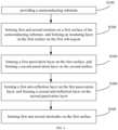
- an embodiment of a method for preparing a solar cell is provided, which can be used to prepare the solar cell described in the first aspect.
- the preparation method includes S100 and S200:
- a semiconducting substrate In S100, a semiconducting substrate is provided.
- the semiconducting substrate includes a first surface and a second surface opposite to each other.
- the semiconducting substrate includes a first region and a second region arranged adjacent to each other in a first direction.
- the first region includes a first sub-region and a second sub-region arranged adjacent to each other in the first direction.
- the first sub-region is in contact with the second region.
- the first direction is perpendicular to the thickness direction of the semiconducting substrate.
- the material of the semiconducting substrate can be silicon. It can be understood that, in S100, a cleaning solution can be used to remove contaminants from the semiconducting substrate. In an example, the cleaning solution is an alkaline solution.
- first and second emitters are formed on the first surface, and an insulating layer is formed on the first emitter and on the first sub-region.
- the first emitter is formed on the first region.
- the second emitter includes a first sub-emitter and a second sub-emitter, and the first and second sub-emitters are connected with each other.
- the first sub-emitter is formed on the second region.
- the second sub-emitter is formed on the insulating layer. Electrical conduction is formed between the first emitter and the first sub-emitter, so as to form a current leakage path.
- the insulating layer is formed on the first emitter, the first sub-emitter of the second emitter is located on the second region, the second sub-emitter of the second emitter is formed on the insulating layer, and a current leakage path is formed between the first emitter and the first sub-emitter.
- the insulating layer is sandwiched between the first emitter and the second sub-emitter, the current leakage area between the first emitter and the second emitter can be reduced, thereby reducing the leakage current, which is conducive to enhancing the working efficiency of the solar cell. Moreover, during the preparation process of the solar cell, the insulating layer can also protect the first emitter, reducing damage to the first emitter in the preparation process, thus improving the structural integrity of the first emitter, which is thus beneficial for improving the performance of the solar cell.
- S200 specifically includes S210 to S250.
- a first tunneling material layer, a first emitter material layer, and a first silicon oxide dielectric material layer are formed as a stack on the first surface, and the semiconducting substrate with the stacked layers is subjected to a first heat treatment.
- the first tunneling material layer can be formed by using a plasma oxidation method or a thermal oxidation method.
- the first emitter material layer can be formed by one of the following two methods.
- the first method the first emitter material layer is formed by using plasma enhanced chemical vapor deposition (PECVD), and the first emitter material layer can be formed to contain a doping element (such as boron or phosphorus); then, the first silicon oxide dielectric material layer is deposited on the first emitter material layer by using PECVD.
- PECVD plasma enhanced chemical vapor deposition
- the first emitter material layer is formed by using low pressure chemical vapor deposition (LPCVD), and the first emitter material layer may contain or not contain any doping element (such as boron or phosphorus).
- LPCVD low pressure chemical vapor deposition
- the first heat treatment can be carried out at a temperature ranging from 700°C to 1100°C. If the first emitter material layer is formed using the first method as described above, the first heat treatment activates the doping element (such as boron or phosphorus) contained in the first emitter material layer, with the first silicon oxide dielectric material layer serving as a protection. If the first emitter material layer is formed using the second method as described above, there can be two scenarios.
- the doping element such as boron or phosphorus
- the first heat treatment not only activates the doping element (such as boron or phosphorus), but also forms a first silicon oxide dielectric material layer on the first emitter material layer due to the high-temperature oxidation by the first heat treatment.
- the doping element can be externally introduced into the first emitter material layer during the first heat treatment, for example, through boron diffusion or phosphorus diffusion, and thus the first silicon oxide dielectric material layer also can be formed during the first heat treatment.
- the material of the first tunneling material layer is silicon oxide
- the material of the initially deposited first emitter material layer is a mixture of microcrystalline silicon and amorphous silicon.
- the mixture of microcrystalline silicon and amorphous silicon further crystallizes to form a crystallized silicon material layer containing a dopant.
- the first silicon oxide dielectric material layer, the first emitter material layer, and the first tunneling material layer on the second region are removed.
- the above regions of layers can be removed by using laser etching or wet etching.
- a second tunneling material layer, a second emitter material layer, and a second silicon oxide dielectric material layer are formed as a stack on the first surface, and the semiconducting substrate with the stacked layers is subjected to a second heat treatment.
- the second tunneling material layer can be formed by using a plasma oxidation method or a thermal oxidation method.
- the second emitter material layer can be formed by one of the following two methods.
- the first method the second emitter material layer is formed by using PECVD.
- the second emitter material layer can be formed to contain a doping element, which is different from the doping element contained in the first emitter material layer in doping type. For example, when the doping element of the first emitter material layer is boron, the doping element of the second emitter material layer is phosphorus, and vice versa.
- the second silicon oxide dielectric material layer is deposited on the second emitter material layer by using PECVD.
- the second emitter material layer is formed by using LPCVD, and the second emitter material layer may contain or not contain any doping element.
- the doping element contained in the second emitter material layer is different from the doping element contained in the first emitter material layer in doping type. For example, when the doping element of the first emitter material layer is boron, the doping element of the second emitter material layer is phosphorus, and vice versa.
- the second heat treatment can be carried out at a temperature ranging from 700°C to 1100°C. If the second emitter material layer is formed using the first method as described above, the second heat treatment activates the doping element (such as boron or phosphorus) contained in the second emitter material layer, with the second silicon oxide dielectric material layer serving as a protection. If the second emitter material layer is formed using the second method as described above, there can be two scenarios.
- the doping element such as boron or phosphorus
- the second heat treatment not only activates the doping element (such as boron or phosphorus), but also forms a second silicon oxide dielectric material layer on the second emitter material layer due to the high-temperature oxidation by the second heat treatment.
- a doping element such as boron or phosphorus
- the doping element can be externally introduced into the second emitter material layer during the second heat treatment, for example, through boron diffusion or phosphorus diffusion, noting that the doping element introduced into the second emitter material layer is different from the doping element introduced into the first emitter material layer in doping type, and thus the second silicon oxide dielectric material layer also can be formed during the second heat treatment.
- the doping element such as boron or phosphorus
- the material of the second tunneling material layer is silicon oxide
- the material of the initially deposited second emitter material layer is a mixture of microcrystalline silicon and amorphous silicon.
- the mixture of microcrystalline silicon and amorphous silicon further crystallizes to form a crystallized silicon material layer containing a dopant.
- the second silicon oxide dielectric material layer, the second emitter material layer, the second tunneling material layer, and the first silicon oxide dielectric material layer in the second sub-region are removed.
- the above regions of layers can be removed by using laser etching or wet etching.
- the second silicon oxide dielectric material layer on the other regions (including the second region and the first sub-region) on the first surface of the semiconducting substrate is removed.
- the first tunneling layer, the first emitter, the insulating layer, the second tunneling layer, and the second emitter are formed.
- the insulating layer is the first silicon oxide dielectric material layer remaining on the first emitter on the first sub-region.
- the preparation method further includes S300 to S500.
- a first passivation layer is formed on the first surface, and a second passivation layer is formed on the second surface.
- a first anti-reflection layer is formed on the first passivation layer, and a second anti-reflection layer is formed on the second passivation layer.
- first and second electrodes are formed on the first surface.
- conductive pastes can be printed in the areas corresponding to the first and second emitters and then sintered.
- the first and second electrodes burn through the first passivation layer and the first anti-reflection layer to make contact with the first emitter and the second emitter, respectively.
- At least some of the steps can include multiple sub-steps or multiple stages, these sub-steps or stages are not necessarily performed at the same time, but may be performed at different times. These sub-steps or stages are not necessarily to be sequentially performed, but can be performed alternately or in turn with at least some of the sub-steps or stages of other steps.
- an embodiment of a photovoltaic module includes the solar cell described in any of the embodiments of the first aspect.
- the photovoltaic module includes a plurality of solar cells, which can be connected in series through welding strips, thereby aggregating the electrical energy generated by individual solar cells for subsequent transmission.
- the first electrodes of each solar cell are electrically connected to the second electrodes of an adjacent solar cell by welding strips
- the second electrodes of each solar cell are electrically connected to the first electrodes of another adjacent solar cell by conductive strips, so that the solar cells are connected in series.
- the solar cells can be arranged at intervals, or can be stacked together in an imbricated form.
- the photovoltaic module further includes an encapsulation layer and a cover plate (not shown).
- the encapsulation layer is configured to cover the surface of the solar cells connected in series.
- the cover plate is configured to cover the surface of the encapsulation layer away from the solar cells.
- the solar cells are electrically connected to form a whole piece or multiple pieces, such as forming a plurality of cell groups.
- the plurality of cell groups are electrically connected in series and/or in parallel. Specifically, in some embodiments, the plurality of cell groups can be electrically connected through conductive strips.
- the encapsulation layer covers the surface of the solar cells.
- the encapsulation layer can be an organic encapsulation film, such as an ethylene-vinyl acetate copolymer film, a polyethylene-octene elastomer film, or a polyethylene terephthalate film.
- the cover plate can have a light-transmitting function, such as a glass cover plate, a plastic cover plate, or the like.
- an embodiment of a photovoltaic system includes the photovoltaic module in the third aspect.
- the photovoltaic system can be applied to photovoltaic power stations, such as ground power stations, roof power stations, water surface power stations, etc.
- the photovoltaic system can be applied to equipment or devices that use solar energy to generate electricity, such as user solar power supplies, solar street lights, solar cars, solar buildings, etc.
- the application scenarios of the photovoltaic system are not limited to the above, that is, the photovoltaic system can be applied in all fields that need to use solar energy to generate electricity.
- the photovoltaic system can include photovoltaic arrays, a combiner box, and an inverter.
- the photovoltaic array can be an array of multiple photovoltaic modules.
- the multiple photovoltaic modules can form multiple photovoltaic arrays.
- the photovoltaic arrays are connected to the combiner box, which can combine the currents generated by the photovoltaic arrays.
- the combined current flows through the inverter and is converted into the alternating current suitable for the power grid, and then connected to the power grid to realize solar power supply.
Landscapes
- Photovoltaic Devices (AREA)
- Life Sciences & Earth Sciences (AREA)
- Engineering & Computer Science (AREA)
- Sustainable Energy (AREA)
- Sustainable Development (AREA)
Applications Claiming Priority (1)
| Application Number | Priority Date | Filing Date | Title |
|---|---|---|---|
| CN202410118651.4A CN117650188B (zh) | 2024-01-29 | 2024-01-29 | 太阳电池及其制备方法、光伏组件、光伏系统 |
Publications (2)
| Publication Number | Publication Date |
|---|---|
| EP4428932A2 true EP4428932A2 (de) | 2024-09-11 |
| EP4428932A3 EP4428932A3 (de) | 2025-02-12 |
Family
ID=90048061
Family Applications (1)
| Application Number | Title | Priority Date | Filing Date |
|---|---|---|---|
| EP24191111.4A Pending EP4428932A3 (de) | 2024-01-29 | 2024-07-26 | Solarzelle und herstellungsverfahren dafür, fotovoltaisches modul und fotovoltaisches system |
Country Status (6)
| Country | Link |
|---|---|
| US (1) | US20240413259A1 (de) |
| EP (1) | EP4428932A3 (de) |
| JP (1) | JP2024138504A (de) |
| CN (2) | CN118507573A (de) |
| AU (2) | AU2024204845B2 (de) |
| MX (1) | MX2024014818A (de) |
Families Citing this family (4)
| Publication number | Priority date | Publication date | Assignee | Title |
|---|---|---|---|---|
| CN118248748A (zh) * | 2024-03-11 | 2024-06-25 | 天合光能股份有限公司 | 背接触太阳能电池、制备方法及电池组件 |
| CN118099245B (zh) * | 2024-04-22 | 2025-10-31 | 浙江晶科能源有限公司 | 背接触太阳能电池及其制备方法、光伏组件 |
| AU2025234300A1 (en) * | 2024-07-10 | 2026-01-29 | Longi Green Energy Technology Co., Ltd. | Back contact solar cell and method for manufacturing same and photovoltaic module |
| CN120857719B (zh) * | 2025-09-23 | 2026-01-02 | 天合光能股份有限公司 | 太阳能电池及太阳能电池的制备方法 |
Family Cites Families (12)
| Publication number | Priority date | Publication date | Assignee | Title |
|---|---|---|---|---|
| CN102725858B (zh) * | 2010-01-26 | 2015-12-09 | 三洋电机株式会社 | 太阳能电池及其制造方法 |
| NL2010496C2 (en) * | 2013-03-21 | 2014-09-24 | Stichting Energie | Solar cell and method for manufacturing such a solar cell. |
| US9196758B2 (en) * | 2013-12-20 | 2015-11-24 | Sunpower Corporation | Solar cell emitter region fabrication with differentiated p-type and n-type region architectures |
| US9837576B2 (en) * | 2014-09-19 | 2017-12-05 | Sunpower Corporation | Solar cell emitter region fabrication with differentiated P-type and N-type architectures and incorporating dotted diffusion |
| CN216488083U (zh) * | 2021-09-30 | 2022-05-10 | 泰州隆基乐叶光伏科技有限公司 | 一种背接触电池 |
| CN115939240B (zh) * | 2022-12-01 | 2024-08-06 | 隆基绿能科技股份有限公司 | 一种背接触电池及其制造方法、光伏组件 |
| CN116404050A (zh) * | 2023-04-24 | 2023-07-07 | 晶科能源(海宁)有限公司 | 背接触光伏组件及其制造方法 |
| CN116230783B (zh) * | 2023-05-09 | 2023-10-03 | 天合光能股份有限公司 | 太阳能电池、太阳能电池片和光伏组件 |
| CN116525708B (zh) * | 2023-07-05 | 2023-09-12 | 福建金石能源有限公司 | 正面宽带隙掺杂的联合钝化背接触太阳电池及其制备方法 |
| CN116825901B (zh) * | 2023-08-25 | 2023-11-21 | 天合光能股份有限公司 | 太阳能电池及其制备方法、光伏组件以及光伏系统 |
| CN117117023B (zh) * | 2023-10-08 | 2025-11-14 | 天合光能股份有限公司 | 异质结背接触电池及其适用的电池组件 |
| CN117423762B (zh) * | 2023-12-15 | 2024-09-03 | 天合光能股份有限公司 | 太阳电池及其制备方法、光伏组件、光伏系统 |
-
2024
- 2024-01-29 CN CN202410596717.0A patent/CN118507573A/zh active Pending
- 2024-01-29 CN CN202410118651.4A patent/CN117650188B/zh active Active
- 2024-07-15 AU AU2024204845A patent/AU2024204845B2/en active Active
- 2024-07-16 JP JP2024113149A patent/JP2024138504A/ja active Pending
- 2024-07-26 EP EP24191111.4A patent/EP4428932A3/de active Pending
- 2024-08-20 US US18/809,868 patent/US20240413259A1/en active Pending
- 2024-11-28 MX MX2024014818A patent/MX2024014818A/es unknown
-
2025
- 2025-04-24 AU AU2025202898A patent/AU2025202898A1/en active Pending
Also Published As
| Publication number | Publication date |
|---|---|
| MX2024014818A (es) | 2025-08-01 |
| EP4428932A3 (de) | 2025-02-12 |
| AU2024204845B2 (en) | 2025-03-27 |
| JP2024138504A (ja) | 2024-10-08 |
| CN117650188B (zh) | 2024-06-04 |
| AU2024204845A1 (en) | 2024-08-01 |
| AU2025202898A1 (en) | 2025-05-15 |
| CN118507573A (zh) | 2024-08-16 |
| CN117650188A (zh) | 2024-03-05 |
| US20240413259A1 (en) | 2024-12-12 |
Similar Documents
| Publication | Publication Date | Title |
|---|---|---|
| US12490547B2 (en) | Solar cell and photovoltaic module | |
| EP4428932A2 (de) | Solarzelle und herstellungsverfahren dafür, photovoltaisches modul, und photovoltaiches system | |
| EP4411832A2 (de) | Solarzelle und herstellungsverfahren dafür, fotovoltaisches modul und fotovoltaisches system | |
| US12464850B2 (en) | Solar cell, method for manufacturing the same, photovoltaic module and photovoltaic system | |
| JP2023163098A (ja) | 太陽電池およびその製造方法、光起電力モジュール | |
| JP2025121336A (ja) | 太陽電池及びその製造方法、積層電池、並びに光起電力モジュール | |
| EP4629783A1 (de) | Solarzelle, tandemsolarzelle und photovoltaikmodul | |
| US20250169221A1 (en) | Solar cell, photovoltaic module, and photovoltaic system | |
| US20130160840A1 (en) | Solar cell | |
| CN120835619B (zh) | 背接触电池、光伏组件及制备方法 | |
| JP7248856B1 (ja) | 太陽電池および太陽電池の製造方法、光起電力モジュール | |
| US20260040725A1 (en) | Solar cell and photovoltaic module | |
| JP2025169190A (ja) | 太陽電池及び太陽光発電モジュール | |
| CN119364865A (zh) | 太阳能电池及其制备方法、光伏组件 | |
| JP7814575B2 (ja) | 太陽電池及び光起電力モジュール | |
| JP2025121412A (ja) | 太陽電池及び光起電力モジュール | |
| CN118398673A (zh) | 太阳能电池、叠层电池及光伏组件 | |
| JP2017037899A (ja) | 太陽電池セル |
Legal Events
| Date | Code | Title | Description |
|---|---|---|---|
| PUAI | Public reference made under article 153(3) epc to a published international application that has entered the european phase |
Free format text: ORIGINAL CODE: 0009012 |
|
| STAA | Information on the status of an ep patent application or granted ep patent |
Free format text: STATUS: REQUEST FOR EXAMINATION WAS MADE |
|
| 17P | Request for examination filed |
Effective date: 20240726 |
|
| AK | Designated contracting states |
Kind code of ref document: A2 Designated state(s): AL AT BE BG CH CY CZ DE DK EE ES FI FR GB GR HR HU IE IS IT LI LT LU LV MC ME MK MT NL NO PL PT RO RS SE SI SK SM TR |
|
| PUAL | Search report despatched |
Free format text: ORIGINAL CODE: 0009013 |
|
| REG | Reference to a national code |
Ref country code: DE Ref legal event code: R079 Free format text: PREVIOUS MAIN CLASS: H01L0031074500 Ipc: H10F0010165000 |
|
| AK | Designated contracting states |
Kind code of ref document: A3 Designated state(s): AL AT BE BG CH CY CZ DE DK EE ES FI FR GB GR HR HU IE IS IT LI LT LU LV MC ME MK MT NL NO PL PT RO RS SE SI SK SM TR |
|
| RIC1 | Information provided on ipc code assigned before grant |
Ipc: H10F 10/165 20250101AFI20250114BHEP |