EP4428896A1 - Device and method for calibrating a charged-particle beam - Google Patents
Device and method for calibrating a charged-particle beam Download PDFInfo
- Publication number
- EP4428896A1 EP4428896A1 EP24162043.4A EP24162043A EP4428896A1 EP 4428896 A1 EP4428896 A1 EP 4428896A1 EP 24162043 A EP24162043 A EP 24162043A EP 4428896 A1 EP4428896 A1 EP 4428896A1
- Authority
- EP
- European Patent Office
- Prior art keywords
- target
- registering
- particle
- charged
- calibration device
- Prior art date
- Legal status (The legal status is an assumption and is not a legal conclusion. Google has not performed a legal analysis and makes no representation as to the accuracy of the status listed.)
- Pending
Links
- 239000002245 particle Substances 0.000 title claims abstract description 89
- 238000000034 method Methods 0.000 title claims description 55
- 238000012545 processing Methods 0.000 claims abstract description 33
- 230000003287 optical effect Effects 0.000 claims description 18
- 239000000758 substrate Substances 0.000 claims description 17
- 230000008569 process Effects 0.000 claims description 15
- 239000012528 membrane Substances 0.000 claims description 14
- 239000011295 pitch Substances 0.000 claims description 9
- 238000003384 imaging method Methods 0.000 claims description 7
- 230000001351 cycling effect Effects 0.000 claims description 2
- 238000005192 partition Methods 0.000 claims description 2
- 238000012937 correction Methods 0.000 abstract description 10
- 230000002441 reversible effect Effects 0.000 abstract description 6
- 238000010894 electron beam technology Methods 0.000 description 22
- 230000006870 function Effects 0.000 description 18
- 230000032683 aging Effects 0.000 description 11
- 238000001459 lithography Methods 0.000 description 11
- XUIMIQQOPSSXEZ-UHFFFAOYSA-N Silicon Chemical compound [Si] XUIMIQQOPSSXEZ-UHFFFAOYSA-N 0.000 description 10
- 238000005259 measurement Methods 0.000 description 10
- 229910052710 silicon Inorganic materials 0.000 description 10
- 239000010703 silicon Substances 0.000 description 10
- 239000000463 material Substances 0.000 description 8
- 235000012431 wafers Nutrition 0.000 description 8
- 239000010410 layer Substances 0.000 description 7
- 230000005405 multipole Effects 0.000 description 6
- 230000035945 sensitivity Effects 0.000 description 6
- 238000011161 development Methods 0.000 description 5
- 230000018109 developmental process Effects 0.000 description 5
- 230000008901 benefit Effects 0.000 description 4
- 150000002500 ions Chemical class 0.000 description 4
- 239000011159 matrix material Substances 0.000 description 4
- 238000013459 approach Methods 0.000 description 3
- 239000011248 coating agent Substances 0.000 description 3
- 238000000576 coating method Methods 0.000 description 3
- 230000000694 effects Effects 0.000 description 3
- 238000000605 extraction Methods 0.000 description 3
- -1 hydrogen ions Chemical class 0.000 description 3
- 238000005286 illumination Methods 0.000 description 3
- 230000009467 reduction Effects 0.000 description 3
- 239000013598 vector Substances 0.000 description 3
- XKRFYHLGVUSROY-UHFFFAOYSA-N Argon Chemical compound [Ar] XKRFYHLGVUSROY-UHFFFAOYSA-N 0.000 description 2
- RTAQQCXQSZGOHL-UHFFFAOYSA-N Titanium Chemical compound [Ti] RTAQQCXQSZGOHL-UHFFFAOYSA-N 0.000 description 2
- 230000003679 aging effect Effects 0.000 description 2
- 239000003990 capacitor Substances 0.000 description 2
- 230000005684 electric field Effects 0.000 description 2
- 238000005421 electrostatic potential Methods 0.000 description 2
- 239000001257 hydrogen Substances 0.000 description 2
- 229910052739 hydrogen Inorganic materials 0.000 description 2
- 230000006872 improvement Effects 0.000 description 2
- 238000011065 in-situ storage Methods 0.000 description 2
- 230000033001 locomotion Effects 0.000 description 2
- 238000004519 manufacturing process Methods 0.000 description 2
- 239000010936 titanium Substances 0.000 description 2
- 229910052719 titanium Inorganic materials 0.000 description 2
- 230000007704 transition Effects 0.000 description 2
- UFHFLCQGNIYNRP-UHFFFAOYSA-N Hydrogen Chemical compound [H][H] UFHFLCQGNIYNRP-UHFFFAOYSA-N 0.000 description 1
- 230000004075 alteration Effects 0.000 description 1
- 229910052786 argon Inorganic materials 0.000 description 1
- 230000005540 biological transmission Effects 0.000 description 1
- 239000013590 bulk material Substances 0.000 description 1
- 238000004364 calculation method Methods 0.000 description 1
- 150000001722 carbon compounds Chemical class 0.000 description 1
- 230000008859 change Effects 0.000 description 1
- 230000007547 defect Effects 0.000 description 1
- 230000008021 deposition Effects 0.000 description 1
- 239000012799 electrically-conductive coating Substances 0.000 description 1
- 238000001900 extreme ultraviolet lithography Methods 0.000 description 1
- 230000002349 favourable effect Effects 0.000 description 1
- 239000007789 gas Substances 0.000 description 1
- 239000001307 helium Substances 0.000 description 1
- 229910052734 helium Inorganic materials 0.000 description 1
- 238000007654 immersion Methods 0.000 description 1
- 238000000671 immersion lithography Methods 0.000 description 1
- 230000010365 information processing Effects 0.000 description 1
- 238000007689 inspection Methods 0.000 description 1
- 230000003993 interaction Effects 0.000 description 1
- 230000001678 irradiating effect Effects 0.000 description 1
- 230000001788 irregular Effects 0.000 description 1
- 238000002955 isolation Methods 0.000 description 1
- 229910052751 metal Inorganic materials 0.000 description 1
- 239000002184 metal Substances 0.000 description 1
- 230000001151 other effect Effects 0.000 description 1
- 230000003647 oxidation Effects 0.000 description 1
- 238000007254 oxidation reaction Methods 0.000 description 1
- 238000001020 plasma etching Methods 0.000 description 1
- 238000012805 post-processing Methods 0.000 description 1
- 239000011241 protective layer Substances 0.000 description 1
- 239000004065 semiconductor Substances 0.000 description 1
- 238000007493 shaping process Methods 0.000 description 1
- 230000007480 spreading Effects 0.000 description 1
- 238000003892 spreading Methods 0.000 description 1
- 238000013519 translation Methods 0.000 description 1
- 238000011144 upstream manufacturing Methods 0.000 description 1
- 229910052724 xenon Inorganic materials 0.000 description 1
- FHNFHKCVQCLJFQ-UHFFFAOYSA-N xenon atom Chemical compound [Xe] FHNFHKCVQCLJFQ-UHFFFAOYSA-N 0.000 description 1
Images


Classifications
-
- H—ELECTRICITY
- H01—ELECTRIC ELEMENTS
- H01J—ELECTRIC DISCHARGE TUBES OR DISCHARGE LAMPS
- H01J37/00—Discharge tubes with provision for introducing objects or material to be exposed to the discharge, e.g. for the purpose of examination or processing thereof
- H01J37/02—Details
- H01J37/04—Arrangements of electrodes and associated parts for generating or controlling the discharge, e.g. electron-optical arrangement or ion-optical arrangement
- H01J37/147—Arrangements for directing or deflecting the discharge along a desired path
- H01J37/1472—Deflecting along given lines
- H01J37/1474—Scanning means
-
- H—ELECTRICITY
- H01—ELECTRIC ELEMENTS
- H01J—ELECTRIC DISCHARGE TUBES OR DISCHARGE LAMPS
- H01J37/00—Discharge tubes with provision for introducing objects or material to be exposed to the discharge, e.g. for the purpose of examination or processing thereof
- H01J37/30—Electron-beam or ion-beam tubes for localised treatment of objects
- H01J37/304—Controlling tubes by information coming from the objects or from the beam, e.g. correction signals
- H01J37/3045—Object or beam position registration
-
- H—ELECTRICITY
- H01—ELECTRIC ELEMENTS
- H01J—ELECTRIC DISCHARGE TUBES OR DISCHARGE LAMPS
- H01J37/00—Discharge tubes with provision for introducing objects or material to be exposed to the discharge, e.g. for the purpose of examination or processing thereof
- H01J37/02—Details
- H01J37/04—Arrangements of electrodes and associated parts for generating or controlling the discharge, e.g. electron-optical arrangement or ion-optical arrangement
- H01J37/147—Arrangements for directing or deflecting the discharge along a desired path
-
- H—ELECTRICITY
- H01—ELECTRIC ELEMENTS
- H01J—ELECTRIC DISCHARGE TUBES OR DISCHARGE LAMPS
- H01J37/00—Discharge tubes with provision for introducing objects or material to be exposed to the discharge, e.g. for the purpose of examination or processing thereof
- H01J37/02—Details
- H01J37/04—Arrangements of electrodes and associated parts for generating or controlling the discharge, e.g. electron-optical arrangement or ion-optical arrangement
- H01J37/045—Beam blanking or chopping, i.e. arrangements for momentarily interrupting exposure to the discharge
-
- H—ELECTRICITY
- H01—ELECTRIC ELEMENTS
- H01J—ELECTRIC DISCHARGE TUBES OR DISCHARGE LAMPS
- H01J37/00—Discharge tubes with provision for introducing objects or material to be exposed to the discharge, e.g. for the purpose of examination or processing thereof
- H01J37/02—Details
- H01J37/244—Detectors; Associated components or circuits therefor
-
- H—ELECTRICITY
- H01—ELECTRIC ELEMENTS
- H01J—ELECTRIC DISCHARGE TUBES OR DISCHARGE LAMPS
- H01J37/00—Discharge tubes with provision for introducing objects or material to be exposed to the discharge, e.g. for the purpose of examination or processing thereof
- H01J37/30—Electron-beam or ion-beam tubes for localised treatment of objects
- H01J37/317—Electron-beam or ion-beam tubes for localised treatment of objects for changing properties of the objects or for applying thin layers thereon, e.g. for ion implantation
- H01J37/3174—Particle-beam lithography, e.g. electron beam lithography
- H01J37/3177—Multi-beam, e.g. fly's eye, comb probe
-
- H—ELECTRICITY
- H01—ELECTRIC ELEMENTS
- H01J—ELECTRIC DISCHARGE TUBES OR DISCHARGE LAMPS
- H01J2237/00—Discharge tubes exposing object to beam, e.g. for analysis treatment, etching, imaging
- H01J2237/02—Details
- H01J2237/024—Moving components not otherwise provided for
-
- H—ELECTRICITY
- H01—ELECTRIC ELEMENTS
- H01J—ELECTRIC DISCHARGE TUBES OR DISCHARGE LAMPS
- H01J2237/00—Discharge tubes exposing object to beam, e.g. for analysis treatment, etching, imaging
- H01J2237/245—Detection characterised by the variable being measured
- H01J2237/24507—Intensity, dose or other characteristics of particle beams or electromagnetic radiation
-
- H—ELECTRICITY
- H01—ELECTRIC ELEMENTS
- H01J—ELECTRIC DISCHARGE TUBES OR DISCHARGE LAMPS
- H01J2237/00—Discharge tubes exposing object to beam, e.g. for analysis treatment, etching, imaging
- H01J2237/245—Detection characterised by the variable being measured
- H01J2237/24564—Measurements of electric or magnetic variables, e.g. voltage, current, frequency
-
- H—ELECTRICITY
- H01—ELECTRIC ELEMENTS
- H01J—ELECTRIC DISCHARGE TUBES OR DISCHARGE LAMPS
- H01J2237/00—Discharge tubes exposing object to beam, e.g. for analysis treatment, etching, imaging
- H01J2237/26—Electron or ion microscopes
- H01J2237/282—Determination of microscope properties
- H01J2237/2826—Calibration
-
- H—ELECTRICITY
- H01—ELECTRIC ELEMENTS
- H01J—ELECTRIC DISCHARGE TUBES OR DISCHARGE LAMPS
- H01J2237/00—Discharge tubes exposing object to beam, e.g. for analysis treatment, etching, imaging
- H01J2237/30—Electron or ion beam tubes for processing objects
- H01J2237/304—Controlling tubes
- H01J2237/30433—System calibration
- H01J2237/30438—Registration
- H01J2237/30444—Calibration grids
-
- H—ELECTRICITY
- H01—ELECTRIC ELEMENTS
- H01J—ELECTRIC DISCHARGE TUBES OR DISCHARGE LAMPS
- H01J2237/00—Discharge tubes exposing object to beam, e.g. for analysis treatment, etching, imaging
- H01J2237/30—Electron or ion beam tubes for processing objects
- H01J2237/304—Controlling tubes
- H01J2237/30433—System calibration
- H01J2237/3045—Deflection calibration
-
- H—ELECTRICITY
- H01—ELECTRIC ELEMENTS
- H01J—ELECTRIC DISCHARGE TUBES OR DISCHARGE LAMPS
- H01J2237/00—Discharge tubes exposing object to beam, e.g. for analysis treatment, etching, imaging
- H01J2237/30—Electron or ion beam tubes for processing objects
- H01J2237/317—Processing objects on a microscale
- H01J2237/3175—Lithography
- H01J2237/31774—Multi-beam
Definitions
- the invention relates to certain improvements in the control of process parameters in a multi-beam charged particle processing apparatus. More specifically, the invention relates to a method for calibrating a charged-particle beam, in particular an electron beam, in a charged-particle processing apparatus or charged-particle multi-beam processing apparatus, which is configured for the exposure of a target by means of a structured beam of electrically charged particles.
- a particle beam is generated in a charged-particle source, is directed to and illuminates a pattern definition device comprising an aperture array composed of a multitude of blanking apertures through which the particle beam penetrates, and is then imaged by a projection optics system onto a target, for writing a desired pattern on the target by exposing a multitude of pixels by means of the particle beam impinging on the target within a beam field of the target.
- the applicant has realized charged-particle multi-beam tools of the mentioned type and developed corresponding charged-particle optics, pattern definition (PD) device, and multi-beam writing method, in particular a 50keV electron multi-beam writer to realize leading-edge complex photomasks for 193nm immersion lithography, masks for EUV lithography and templates (1x masks) for imprint lithography.
- the system is called eMET (electron Mask Exposure Tool) or MBMW (multi-beam mask writer) for exposing 6" mask blank substrates.
- the multi-beam system has been called PML2 (Projection Mask-Less Lithography) for electron beam direct writer (EBDW) applications on Silicon wafer substrates.
- the multi-beam column and writing method can also be used for multi-beam inspection applications.
- lithographic apparatus 1 Exemplary schematics of the multi-beam writer are shown in Fig. 1 .
- the main components of the lithography apparatus 1 are - corresponding to the direction of the lithography beam lb, pb which in this example runs vertically downward in Fig.
- the whole apparatus 1 is contained in a vacuum housing 2 held at high vacuum to ensure an unimpeded propagation of the beam lb, pb along the optical axis cw of the apparatus.
- the charged-particle optical systems 3, 5 are realized using electrostatic and/or magnetic lenses.
- the illumination system 3 comprises, for instance, an electron gun 7, an extraction system 8 as well as a condenser lens system 9. It should, however, be noted that in place of electrons, in general, other electrically charged particles can be used as well. Apart from electrons these can be, for instance, hydrogen ions or heavier ions, charged atom clusters, or charged molecules.
- the extraction system 8 accelerates the particles to a defined energy of typically several keV, e.g. 5 keV.
- a condenser lens system 9 By means of a condenser lens system 9, the particles emitted from the source 7 are formed into a wide, substantially telecentric particle beam 50 serving as lithography beam lb.
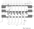
- the lithography beam lb then irradiates a PD system 4 which comprises a number of plates with a plurality of openings or apertures 24 ( Fig. 2 ).
- the PD system 4 is held at a specific position in the path of the lithography beam lb, which thus irradiates the plurality of apertures and is split up into a number of beamlets.
- some of the apertures 24 of the PD system 4 are "switched on” or “open” so as to be transparent to the incident beam in the sense that they allow the portion of the beam (beamlets 51) that is transmitted through it to reach the target; the other apertures are “switched off” or “closed”, i.e. the corresponding beamlets 52 cannot reach the target, and thus effectively these apertures and/or openings are non-transparent (opaque) to the beam.
- the lithography beam lb is structured into a patterned beam pb, emerging from the PD system 4.
- the pattern of switched on apertures - the only portions of the PD system 4 which are transparent to the lithography beam lb - is chosen according to a pattern which is to be exposed on the target 16. It has to be noted that the "switching on/off" of the beamlets usually is realized by some sort of deflection means provided in one of the plates of the PD system 4: “Switched off"-beamlets are deflected off their path (by very small angles) so they cannot reach the target but are merely absorbed somewhere in the lithography apparatus, e.g. by an absorbing plate 11.
- the pattern as represented by the patterned beam pb is then projected by means of an electro-magneto-optical projection system 5 onto the substrate 16 where it forms an image of the "switched-on" apertures and/or openings.
- the projection system 5 implements a demagnification of, for instance, 200:1 with two crossovers c1 and c2.
- the substrate 16 used as target is, for instance, a 6" mask blank or a silicon wafer covered with a particle sensitive resist layer 17.
- the target is held by a chuck 15 and positioned by a substrate stage 14 of the target station 6.
- the terms "substrate” and “target” are used interchangeably, referring to any substrate placed at the target position in the processing apparatus.
- the information regarding the pattern to be exposed is supplied to the PD system 4 by a data path realized by means of an electronic pattern information processing system 18 (see also the description of the data path below).
- the projection system 5 is composed of a number of consecutive electro-magneto-optical projector stages 10a, 10b, 10c, consisting of electrostatic and/or magnetic lenses and other deflection means, and is controlled by a projections controller 56, which is, for instance, a dedicated controlling computer or part of an optics controller (not shown) of the entire apparatus 1. These lenses and means are shown in symbolic form only, since their application is well known in the prior art.
- the projection system 5 employs a demagnifying imaging through crossovers c1, c2.
- the demagnification factor for both stages is chosen to achieve an overall demagnification of several hundreds, e.g. 200: 1.
- a demagnification of this order is in particular suitable with a lithography setup, in order to alleviate problems of miniaturization in the PD device.
- deflection means 12a, 12b and 12c are provided in the condenser 3 and projection system 5.
- the deflection means can be realized as, for instance, a multipole electrode system which is positioned near the source extraction system (12a), near the first crossover, as shown in Fig. 1 with the deflection means 12b, and/or after the final lens 10c of the respective projector, as in the case with the stage deflection means 12c in Fig. 1 .
- a multipole electrode arrangement is used as deflection means both for shifting the image in relation to the stage motion and for correction of the imaging system in conjunction with the charged-particle optics alignment system.
- deflection means 12a, 12b, 12c are not to be confused with the deflection array means of the PD system 4 which, in conjunction with the stopping plate 11, are used to switch selected beamlets of the patterned beam pd to "on" or "off” state, since the former only deal with the particle beam as a whole.
- the PD system 4 preferably comprises three plates stacked in a consecutive configuration: An "Aperture Array Plate” (AAP) 20, a “Deflection Array Plate” (DAP) 30 and a “Field-boundary Array Plate” (FAP) 40.
- AAP ture Array Plate
- DAP Deflect Array Plate
- FAP Field-boundary Array Plate
- a 'plate' refers to an overall shape of the respective device, but does not necessarily indicate that a plate is realized as a single plate component even though the latter is usually the preferred way of implementation; still, in certain embodiments, a 'plate', such as the aperture array plate, may be composed of a number of sub-plates, for instance, two movable sub-plates which enable beamlet sizes switchable in-situ, cf. US 8,546,767 by the applicant.
- the plates are preferably arranged parallel to each other, at mutual distances along the Z direction.
- the flat upper surface of AAP 20 forms a defined potential interface to the condenser optics/illumination system 11.
- the AAP may, e.g. be made from a square or rectangular piece of a silicon wafer (approx. 1mm thickness) 21 with a thinned center part 22.
- the plate may be covered by an electrically conductive protective layer 23 which will be particularly advantageous when using hydrogen or helium ions (cf. US 6,858,118 ).
- the layer 23 may also be of silicon provided by the surface section of 21 and 22, respectively, so that there is no interface between layer 23 and bulk parts 21,22, respectively.
- the AAP 20 is provided with a plurality of apertures 24 realized as openings traversing the thinned part 22.
- the apertures 24 are realized having a straight profile fabricated into the layer 23 and a "retrograde" profile in the bulk layer of the AAP 20 such that the downward outlets 25 of the openings are wider than in the main part of the apertures 24.
- Both the straight and retrograde profiles can be fabricated with state-of-the-art structuring techniques such as reactive ion etching.
- the retrograde profile strongly reduces mirror charging effects of the beam passing through the opening.
- the DAP 30 is a plate provided with a plurality of openings 33, whose positions correspond to those of the apertures 24 in the AAP 20, and which are provided with electrodes 35, 38 configured for deflecting the individual sub-beams passing through the openings 33 selectively from their respective paths.
- the DAP 30 can, for instance, be fabricated by post-processing a CMOS wafer with an ASIC circuitry.
- the DAP 30 is, for instance, made from a piece of a CMOS wafer having a square or rectangular shape and comprises a thicker part 31 forming a frame holding a center part 32 which has been thinned (but may be suitably thicker as compared to the thickness of 22).
- CMOS electronics 34 is used to control the electrodes 35, 38, which are provided by means of MEMS techniques. Adjacent to each opening 33, a "ground" electrode 35 and a deflection electrode 38 are provided.
- the ground electrodes 35 are electrically interconnected, connected to a common ground potential, and comprise a retrograde part 36 to prevent charging and an isolation section 37 in order to prevent unwanted shortcuts to the CMOS circuitry.
- the ground electrodes 35 may also be connected to those parts of the CMOS circuitry 34 which are at the same potential as the silicon bulk portions 31 and 32.
- the deflection electrodes 38 are configured to be selectively applied an electrostatic potential; when such electrostatic potential is applied to an electrode 38, this will generate an electric field causing a deflection upon the corresponding sub-beam, deflecting it off its nominal path.
- the electrodes 38 as well may have a retrograde section 39 in order to avoid charging.
- Each of the electrodes 38 is connected at its lower part to a respective contact site within the CMOS circuitry 34.
- the height of the ground electrodes 35 is higher than the height of the deflection electrodes 38 in order to suppress cross-talk effects between the beams.
- a PD system 12 with a DAP 30 having electrodes oriented downstream as shown in Fig. 2 is only one of several possibilities. Further DAP configurations, e.g. with embedded ground and deflection electrodes, can easily be devised by the skilled person (see other patents in the name of the applicant, such as US 8,198,601 ).
- the third plate 40 serving as FAP has a flat surface facing to the first lens part of the downstream demagnifying charged-particle projection optics and thus provides a defined potential interface to the first lens 16a of the projection optics.
- the thicker part 41 of FAP 40 is a square or rectangular frame made from a part of a silicon wafer, with a thinned center section 42.
- the FAP 40 is provided with a plurality of openings 43 which correspond to the openings 24, 33 of the AAP 20 and DAP 30 but are wider as compared to the latter.
- the PD system 4, and in particular the first plate thereof, the AAP 20, is illuminated by a broad charged particle beam 50 (herein, "broad" beam means that the beam is sufficiently wide to cover the entire area of the aperture array formed in the AAP), which is thus divided into many thousands of micrometer-sized beams 51 when transmitted through the apertures 24.
- the beamlets 51 and 52 will traverse the DAP and FAP unhindered.
- a deflection electrode 38 is powered through the CMOS electronics, an electric field will be generated between the deflection electrode and the corresponding ground electrode, leading to a small but sufficient deflection of the respective beam 52 passing through ( Fig. 2 ).
- the deflected beam can traverse the DAP and FAP unhindered as the openings 33 and 43, respectively, are made sufficiently wide. However, the deflected beam 52 is filtered out at the stopping plate 15 of the sub-column ( Fig. 1 ). Thus, only those beams which are unaffected by the DAP will reach the target.
- the reduction factor of the demagnifying charged-particle optics 5 is chosen suitably in view of the dimensions of the beams and their mutual distance in the PD device 4 and the desired dimensions of the structures at the target. This will allow for micrometer-sized beams at the PD system whereas nanometer-sized beams are projected onto the target.
- the ensemble of (unaffected) beams 51 as formed by AAP is projected to the target with a predefined reduction factor R of the projection charged-particle optics.
- the individual beams 51, 52 depicted in Fig. 2 are representative of a much larger number of sub-beams, typically many thousands, arranged in a two-dimensional X-Y array.
- resist covered 150mm Si wafers are examples of resist covered 150mm Si wafers.
- the first generation MBMW production tools are targeted to use 20nm and 10nm beams providing up to approx. 1 ⁇ A current for all 262,144 programmable beams "on".
- For following generations of MBMW production tools there is the plan to use even smaller beam size of e.g. 8nm and concurrently to provide e.g. 640 ⁇ 640 409,600 beamlets within the 81.92 ⁇ m ⁇ 81.92 ⁇ m beam field at the target.
- the above-stated aim is met by a method for calibrating a charged-particle beam in a charged-particle processing apparatus in relation to a positioning of the charged-particle beam with respect to a target plane of the processing apparatus, wherein the method comprises the steps of
- the central relative position obtained in the last mentioned step may be used for deflecting the beam back to the designated target position using a reverse lateral deflection which includes an inverse of the initial deflection combined with a deflection correction, which deflection correction represents a correction of the lateral beam position to compensate the central relative position.
- This may, in particular, serve to compensate for drifts of the lateral position of the beam.
- This method provides a efficacious approach for determining and/or implementing a calibration position of the beam, which also allows compensating of drifts within the charged-particle processing apparatus.
- particles arriving (at the registering structure) means that these particles hit the shape of the respective registering structure so as to contribute to the signal of measurement.
- the charged particles may be electrons, and then the beam calibration device is configured to detect electrons.
- the method according to the invention can also be used for determining a "distortion" of the beam at the target position, where “distortion” refers to a variation of focal properties across the area of the beam (different beamlet constituting the beam), and thus can contribute to better detect the presence and amounts of imaging defects of the image field generated by the beam on the target.
- the invention in particular the method according to the invention, may also include in particular one or more of the following developments.
- the evaluating step may include fitting an pre-selected function to the measured current signal, obtaining optimal fitting parameters from which to determine a center location of the signal curve (which represents the signal intensity as function of the position).
- the steps of deflecting the beam and performing a scan are realized by using a beam deflection device of the charged-particle processing apparatus (this beam deflection device is, typically, positioned upstream of the target plane) and wherein, in the step of performing a scan, the beam is deflected across the registering structure through a plurality of scanning positions in accordance with a predefined grid of positions.
- This grid may, preferably, have a grid pitch (mesh width) that is either smaller than the nominal size of a beamlet spot as produced by a single beamlet in the target plane (for instance, by a factor 1/2 n where n is an integer, or half-integer in the case of a double-centered grid raster as illustrated in Fig.
- the grid pitch may also be larger than the beamlet spot nominal size, for instance double size or a convenient multiple (such a factor 2 n where n is an integer, or half-integer in the case of a double-centered grid raster).
- the step of performing a scan is repeated, so as to have multiple instances of the scanning step, that, based on a predetermined (conceptual) partition of the grid of positions into a number of mutually distinct subsets, which represent sub-grids that preferably are substantially equivalent, in each instance of the step of performing a scan, one of these subsets is used; this means that the beam is deflected only through scanning positions corresponding to the respective subset (in one instance); and in case the scanning step is repeated, subsequent instances of the step of performing a scan use respectively different subsets, thus cycling through the number of subsets.
- the grid used for performing the scan may be composed of grid areas having different mesh widths, that is, at least two grid areas having different grid pitches; preferably, the grid areas having a larger grid pitch are defined in regions that are less significant for the quality of the determination of a central relative position.
- the calibration method of the invention may suitably be performed during or immediately before a writing process on a substrate provided at the designated target position. This can ensure an enhanced precision of the respective writing process and avoids intervening disturbing contributions to drift.
- the calibration method of the invention is of particular advantage for use a in a charged-particle optical apparatus realized as a multi-column system.
- a system will comprise a plurality of particle-optical columns configured for processing simultaneously on the same target, which is positioned in the target plane: advantageously a plurality of beam calibration devices may be provided, to be positioned longitudinally at or close to the plane of a target at a position lateral to the target and preferably separate from the target; for each of the beams, or each of a selected subset of the beams, that belong to a number of particle-optical columns (this number preferably corresponding to the number of beam calibration devices), the above-described method steps of deflecting the beam, performing a scan, and measuring an electric current caused by the beam will then be carried out using a respective one of the beam calibration devices.
- a number of beams can be simultaneously calibrated using a number of beam calibration devices.
- a further advantageous development of the method may use a number of mutually different beam portions of the beam (each of these portions may be represented by one beamlet or a group of beamlets, where the groups of beamlets representing the beam portions are arranged according to preferably the same arrangement) are used for a corresponding number of calibrations, which are performed subsequently (preferably, but not necessarily immediately subsequently); then, the results of the respective central relative positions thus determined (from said number of calibrations) are used to deduce a distortion or distortion map, describing how different portions of the beam at the designated target position are positioned relative to each other. This may be used for determining a "distortion" of the beam at the target position, as already mentioned.
- a plurality of registering structures are used, which are arranged at respective predetermined locations on the beam calibration device, wherein advantageously the registering structures are substantially aligned with locations of said mutually different beam portions as projected onto the registering structures.
- substantially aligned means that small deviations are allowed which do not impair the accuracy of the calibration measurements.
- a further aspect of the invention is directed at a beam calibration device for calibrating a charged-particle beam in a charged-particle processing apparatus (in particular an electron beam in a processing apparatus employing such an electron beam), which device is in particular used during the method of the invention, wherein this device is configured / intended to be used in such apparatus employing a charged-particle beam (in particular electron beam) of a predetermined type, and the beam calibration device is configured to detect the particles of said specific type and comprises: a registering surface provided with at least one registering structure, oriented substantially perpendicular to an axis direction along which the beam is to be irradiated onto the beam calibration target; and a detector configured to measure the amount of charged particles (which typically may be electrons) arriving at the at least one registering structure as an output signal upon being irradiated by the beam (also here, "particles arriving at a registering structure” means that these particles hit the shape of the respective registering structure so as to contribute to the signal of measurement); the beam calibration device is configured to transmit
- the devices of the invention may also include in particular one or more of the following developments.
- the registering surface may be realized as a membrane, in particular a free-standing membrane, which is provided with at least one registering structure, where such a registering structure is transparent for the charged particles impinging on the registering surface and otherwise impermeable for the charged particles; and the detector is positioned downstream of the registering structure(s) and is configured to measure the amount of charged particles passing through the registering surface.
- the registering surface may suitably be provided with a plurality of registering structures which may have different shapes or may have the same shape when viewed along the optical axis, i.e. the axis direction along which the beam is (to be) irradiated.
- the invention also includes a charged-particle processing apparatus including at least one beam calibration device according to the invention; preferably the beam calibration device is positioned longitudinally at or close to the plane of a target in the processing apparatus and preferably at a lateral offset from a position intended for a target to be processed by the processing apparatus; in particular, one or more beam calibration devices may be disposed at a position external to the target.
- “close to” means that the device may be at a small distance to the relevant plane, which has no significant effect on the imaging properties with respect to the calibration procedure, and in particular that no optical component of the apparatus is between the device and the target plane, as seen along the longitudinal direction.
- the charged-particle processing apparatus may further include a calibration controller, to which the beam calibration device is connectable, and such calibration controller is suitably configured to receive a position signal relating to a relative position of the beam impinging on the beam calibration device and to record the output signal as a function of the relative position and determine therefrom an optimal relative position of the beam.
- a calibration controller to which the beam calibration device is connectable, and such calibration controller is suitably configured to receive a position signal relating to a relative position of the beam impinging on the beam calibration device and to record the output signal as a function of the relative position and determine therefrom an optimal relative position of the beam.
- the charged-particle optical apparatus may also be realized as a multi-column system, which comprises a plurality of particle-optical columns, where each column comprises a respective beam calibration device according to the invention, respectively positioned longitudinally at or close to the plane of a target in the respective column, and preferably at a lateral offset from a target position in the respective column (laterally beside the target of the multi-column system), the multi-column system preferably comprising a calibration controller connected to the beam calibration devices, provided for calibrating charged-particle beams of the particle-optical columns, and advantageously using the respective output signal provided by the respective beam calibration devices and respective position signals relating to relative positions of the respective beams impinging on the respectively corresponding beam calibration devices.
- all beam calibration devices may be arranged in a fixed arrangement, or each of them may be mounted on a respective moveable stage, in order to allow for correction of misalignments between the beam calibration devices according to the arrangement of the single columns.
- the plurality of beam calibration devices may, preferably, be positioned not only longitudinally at or close to the plane of the target, but also at a position lateral to the target and, possibly and advantageously, separate from it.
- the plurality of particle-optical columns may preferably be configured for processing simultaneously on the same target, and in this case each of said plurality of beam calibration devices may suitably be associated with a respective one of said plurality of particle-optical columns or with a respective one of several mutually disjunct groups of particle-optical columns, and is used for performing the calibration for the respectively associated one of these columns (or, respectively, one of the columns of the respectively associated group).
- the beam calibration method is applied in a multibeam writer tool as illustrated in Fig. 1 in order to calibrate the transversal positioning of a shaped charged-particle (electron) beam on the image plane with respect to a reference point, which can, in particular, be used for proper positioning of the beam on a mask substrate loaded into the apparatus at the desired target position.
- the method preferably uses the following device components:
- the mentioned components are controlled by the controller 56 of the writing apparatus 1.
- the beam calibration process uses the signal s 1 generated by the BCT 19 and a signal s 2 which specifies the relative position of the beam as it impinges on the target plane, such as a signal branched-off from the deflection signal that controls the deflection device (symbolized by a wavy line in Fig. 1 ).
- the beam calibration will be performed in a program module of the controller 56 or in a specific calibration controller 59, which cooperates with the controller 56 and may, preferably, be located within the housing 2 of the writing apparatus 1.
- the BCT serves to register the coincidence of a beam with a pre-defined nominal position on the BCT top surface.
- the BCT will be realized as a component mounted to the mask chuck 15 holding a substrate 16 (or other target) and/or the target stage 14. This allows that the BCT is placed to a side of the location of a substrate 16. With respect to the longitudinal direction the BCT is arranged such that its top surface is positioned in the target plane of the electron optical system.
- the BCT top surface will suitably comprise a registering surface oriented towards the incoming beam as described below.
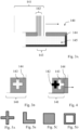
- the BCT 140 comprises a registering surface, for instance a structured top membrane 144, which has a number of registering structures (such as an aperture 143 formed in the membrane 144, or a plurality of such apertures arranged in a specific two-dimensional layout) as well as an electron current measuring device 145, placed below the registering surface (or membrane).
- a registering surface for instance a structured top membrane 144, which has a number of registering structures (such as an aperture 143 formed in the membrane 144, or a plurality of such apertures arranged in a specific two-dimensional layout) as well as an electron current measuring device 145, placed below the registering surface (or membrane).
- Each registering structure is preferably realized as a recess and/or hole formed in the surface of the BCT 19, for instance as an aperture in the top membrane of the BCT.
- the registering structure is an aperture 143 allowing passage of electrons, whereas the other regions of the membrane 144 will block (by absorbing and/or reflecting) any incoming electrons.
- a registering structure may be formed as a shaped recess, thus thinning the membrane in the recess to a thickness which allows the energetic electrons to penetrate, while the other regions of the membrane have a considerably higher thickness (and preferably an additional covering layer as discussed below) so the electrons cannot pass the membrane in the latter regions.
- the shape of a registering structure may be any suitable shape, such as a narrow rectangle (i.e., slit), an L-shape ( Fig. 5B ), a rectangle or square ( Fig. 5C ), a box shape ( Fig. 5D ), or a cross ( Fig. 5A, 3B )
- a preferred process of lateral position calibration comprises the following steps:
- the electron beam is repositioned as needed to correctly place the electron beam on the target 72 at a specific target position as required for a subsequent writing process on a substrate provided in the target position.
- the calibration process is controlled by a calibration controller 59 that controls the mask stage position as well as the deflection device (for instance by controlling the supply voltages of the latter).
- a calibration controller 59 that controls the mask stage position as well as the deflection device (for instance by controlling the supply voltages of the latter).
- the stage is moved approximately so that the electron beam is able to hit the BCT and the deflection device is used for the fine positioning of the beam position on the target and to perform the scanning steps as needed during the writing process.
- the method may also involve using a sensitivity matrix that indicates the required voltages supplied to the deflection device. This will be discussed in more detail further below.
- the calibration controller 59 may be realized as a program module of the controller 56, or as a specific controller device which cooperates with the controller 56 and may, preferably, be located within the housing 2 of the writing apparatus 1.
- the calibration controller 59 uses the signal s 1 generated by the BCT 19 and a signal s 2 which specifies the relative position of the beam as it impinges on the target plane (symbolized by a wavy line in Fig. 1 , as in general this signal s 2 may be a control signal of the deflection device 12c or a signal branched-off from the deflection device control signal).
- the scan is performed for a beam, as formed in the PD device, defined by a single beamlet.
- the beam traverses the electron optical system of the writer tool for performing a lateral position calibration according to the invention.
- the resulting measured current signal scan will produce a map which will generally look like the form of the structure itself (since the convolution of a point-like function with a specific shape simplifies to the very equal shape).
- the shape of a registering structure is a cross ( Fig. 3B )
- the measured current pattern as a function of the transversal coordinates x and y will reproduce this shape as shown in Fig. 7 , if the transversal size of the beam is negligible as compared to the feature size of the cross.
- a typical electron beamlet formed by the pattern definition device Due to the non-zero (finite) size of a typical electron beamlet formed by the pattern definition device, there will be transition zones at the borders of a BCT pattern in the current measurement, illustrated in Fig. 6 , which shows the intensity produced by a simple slit-shape structure when traversing perpendicular to the direction of extension of the slit shape (one-dimensional signal). Since a real electron beamlet formed by the pattern definition device has a non-zero blur, the resulting signal will additionally have blurred out corners (rather than linear flanks as shown in Fig. 6 ).
- Using a single beamlet for the calibration may incur the disadvantage of a low signal-to-noise ratio in the current measurement. This strongly depends on the method of current measurement, as discussed in more detail below.
- Using a beam comprising multiple beamlets can alleviate this problem.
- this offers the additional advantage that the beam may have suitable pattern structure.
- Fig. 3A shows a longitudinal sectional detail view of a BCT 140 at one aperture 144 thereof
- Fig. 3B shows a top view of the BCT aperture
- Fig. 4 illustrates a scan using a shaped beam 142 composed of multiple beamlets, where the beam (more exactly the image of the beam, shown as a dark-shaded cross in the drawing) scans across the registering structure 143 along the direction indicated by an arrow.
- the beam more exactly the image of the beam, shown as a dark-shaded cross in the drawing
- the measured current pattern in two dimensions will typically look like shown in Figs. 8A and 8B .
- Fig. 8A shows an example where the cross-shaped electron beam pattern has exactly the same size as the BCT pattern, whereas in Fig. 8B , the cross-shaped electron beam pattern is smaller.
- the current patterns of Figs. 8A and 8B include considerable transition zones, which are created due to the partial transmission of the group of beamlets at the edges of the aperture.
- the calibration result includes the average deflection of the beamlets.
- the pattern of the beamlets be similar to the shape of the apertures (or more generally, registering structures).
- the BCT also comprises a device for accurately measuring the electron current transmitted through the BCT registering structures; preferably this measuring device should have high precision and a large signal-to-noise ratio.
- the measuring device may be a Faraday cup located downstream of the membrane containing the registering structures.
- other suitable types of devices such as a channeltron or a semiconductor detector.
- the choice of material for the BCT may affect its performance.
- the highest priority for the BCT functionality is the opacity for electrons at regions different from the registering structures, which can be optimized by choosing an adequate thickness of the material.
- the bulk material may be silicon coated with a metal, such as titanium.
- Silicon has the advantage of being well processible (exploiting paramount experience in the processing industry), which strongly facilitates creating the registering structures.
- a coating, for example titanium coating is advantageous for protecting the silicon from oxidation.
- an electrically conductive coating helps to prevent the BCT surface from charging up during electron exposure.
- it is advantageous that the coating is vacuum-compatible.
- the choice of material also has an impact on the backscattering of electrons generated on the BCT surface, which may influence other parts of the writer tool.
- material for example carbon compounds
- aging may be deposited in or at the border of the registering structures, further called aging.
- the recesses or openings may grow closed.
- this aging may be inhomogeneous along the edges of the registering structures due to the exposure positioning of the beamlets.
- An example of aging is illustrated in Fig. 9 , which depicts a slit-shaped registering structure 60 from above, where material of irregular shape 61 has deposited at the inward longitudinal edges. This aging will disturb the current measurement and consequently the center position determined using the "aged" registering structure, up until that a measurement becomes unreliable.
- the aging can be reduced and homogenized so as to reduce or even rule out the problem, as discussed in the following sections.
- the choice of grid positions that are used during a calibration scan may strongly influence the performance of the calibration as well as the above-mentioned aging effect.
- a higher number of grid points provides finer data to be fitted, improving the fit quality, but on the other hand, the scan takes longer.
- the aging effect depends on the placement of the beamlets along the edges of the registering structure.
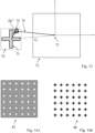
- One possible improvement is to define a dense grid as illustrated in Fig. 10 , so that the deposited electron beam dose over all scan points is homogeneous.
- each of the squares correspond to one beam spot as produced by the beam during the scan, and the entire area is thus completely covered by the beam spots of the grid as also shown in Fig. 10 ("dense grid").
- a sub-grid of the grid may be used, and when the calibration process is performed multiple times, different sub-grids of the same grid are used; this is also referred to as “spreading out” the grid over multiple calibrations. For instance, still referring to Fig. 10 , in one loop of the calibration process, only the beam spots numbered as "1" are used, in a next loop of the calibration, the beam spots numbered "2", in a third loop the beam spots numbered "3", and then "1” is used again and so on. Thus, the entire dense grid is used by a subsequent set of multiple calibrations (in this example, three calibrations). This allows to reduce the number of grid points used during an individual instance of the calibration process, thus reducing the time used by the scan and the complexity of calculation.
- interlocking grids are multiple grids which are positioned interlacing by mutual offsets which are only fractions of a grid spacing (which corresponds to the nominal size of a beamlet spot on the target), which enables creating sub-pixels by allowing the beamlet spots to overlap (for example by 25 or 50 percent of one pixel on the target), thus creating sub-pixels in the pattern raster generated by the beamlets.
- Interlocking grids are described in US 7,276,714 and US 9,053,906 of the applicant in more detail.
- a pixel 70 formed by a first beamlet is overlapping with another pixel 71, and the overlapping region forms a sub-pixel 77, to which the combined dose from the two pixels 70 and 71 is deposited.
- the interlocking grid may also be "spread out" over multiple calibrations. This has the advantage of further homogenizing the electron beam dose that is applied to the edges of the registering structure, because local inhomogeneities of beamlets will average out to considerable extent.
- Figs. 12A and 12B illustrate examples of "thinned-out" scan grids.
- Fig. 12a illustrates an example of a linear scan where the beam pattern illuminates a registering structure that is larger than the beam pattern.
- the grid points in this region 121 have negligible impact on the aging.
- the grid points falling in the region 121 have little significance for the fit quality.
- grid points in such a region can be thinned out. Such a thinning is depicted in Fig.
- Fig. 12A where the grid points in a one dimensional scan example are thinned out in a grid area 122, which is located within the expected range of a plateau.
- Fig. 12B illustrates a two-dimensional example for a square-shaped registering structure. In this example, only the ring-shaped region 123 that is expected to coincide with the locations where a change of signal will occur, is implemented using a grid of small grid pitch, whereas other regions 124, 125, which in the case illustrated in Fig. 12b are inside and outside the region 123, respectively, are "thinned out".
- the deflection device is used to perform precise deflections for a scan.
- the deflection device is, e.g., a electrostatic multi-pole electrode system, allowing realizing a deflection by applying electrical potentials to the individual electrodes.
- the deflection element is a plate capacitor. To deflect in two perpendicular directions, a double plate capacitor may be implemented.
- the deflection device is a multi-pole system having a suitable number of electrodes.
- a preliminary calibration procedure may be used to measure the deflection sensitivity of the deflection element, i.e.
- this sensitivity matrix can be measured in the mentioned preliminary calibration procedure.
- Using the sensitivity matrix enables a suitable approach for controlling predefined deflections, such as r 0 or ⁇ r in Fig. 13 .
- the fit procedure is one step in the calibration process according to the invention, and serves to determine a potential spatial transversal offset such as the offset vector ⁇ r (see Fig. 13 ) between the expected position of the beam center and the actual beam center positioned as measured one.
- the function used for the fit is selected suitably so as to describe the general form of the convoluted measured electron current pattern with sufficient accuracy.
- the fit procedure will include a translation, described by an offset in the two transversal coordinates x and y.
- the accuracy of the fitted offsets is determined by the quality of the fit function, the grid points (number and placement) as well as potential noise on the measured current signal.
- a determined non-zero offset indicates a deflection correction in the optical system (e.g.
- Another example is a fit function having curved flanks, which can be modelled by stitching together suitable functions such as a first sigmoid function for a raising flank and a second sigmoide function for a falling flank.
- suitable functions such as a first sigmoid function for a raising flank and a second sigmoide function for a falling flank.
- suitable fit functions for two-dimensional fits or higher can be provided readily by the skilled person by stitching suitable one-dimensional functions.
- a distortion measurement can be performed, i.e. how different segments of beamlets of the full image-field are positioned relative to each other or relative to ideal positions.
- multiple registering structures may be used.
- a complex BCT having an array of 6 by 6 registering structures 81, which preferably may have the same shape, but may also have different shapes, is used, in conjunction with a beam 80 as shown in Fig. 14B that has a suitable shape, and in particular may be preferably composed of a corresponding array of sub-beams.
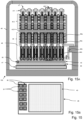
- Figs. 15 A and 15 B illustrate a multi-column writer tool 100.
- the writer tool employs a number of charged particle beams, which may be of electrons or ions (for instance ions of positive electric charge).
- the writer tool 100 comprises a vacuum housing 48 for the multi-column charged particle optics, a base 47 onto which the multi-column charged particle optics is mounted.
- On top of the base an X-Y stage 46, e.g.
- the multi-column writer tool 100 further includes, preferably for each column or each of a subset of the columns, a respective instance of a BCT 90 according to an embodiment of the invention.
- the respective BCTs 90 symbolically depicted as hatched squares in Fig. 15B ) may be placed on the stage 46 beside the target 45.
- the multi-column optics of this embodiment comprises a plurality of sub-columns 400 (the number of columns shown is reduced in the depiction for better clarity, and represent a much larger number of columns that are present in the multi-column apparatus in a realistic implementation).
- the sub-columns have identical setups and are installed side-by-side with mutually parallel axes c5.
- Each sub-column has an illuminating system 412 including a charged particle source 411, delivering a broad telecentric charged-particle beam to a pattern definition system 413 being adapted to let pass the beam only through a plurality of apertures defining the shape of sub-beams ("beamlets") permeating said apertures (beam shaping device), and a typically demagnifying and further energizing charged particle projection optics 44, composed of a number of consecutive charged particle lenses, which preferably include electrostatic and/or magnetic lenses, and possibly other particle-optical devices.
- the projection optics comprises e.g. a first charged particle lens 44a, e.g. an electrostatic immersion lens, whereas a second lens 44b, located downstream of the first lens, may be realized using an charged particle electromagnetic lens.
- Fig. 15B shows, in a detail top view, the lower portion of the multi-column writer tool 40 where multiple BCT devices 90 are located on the stage besides the target.
- Each BCT is positioned longitudinally at or close to the plane of a target.
- a common calibration controller (not shown; cf. controller 59 in Fig. 1 ) is provided which performs and controls the calibration procedures of the charged-particle beams of the particle-optical columns.
- the calibration procedure may be done simultaneously for all of the columns; or if there is not a BCT for each column, a suitable subset of the columns can be calibrated simultaneously and the other columns in subsequent steps.
- the target stage 46 cooperates with a multipole deflector component of e.g. the final lens 44b of the respective columns to generate a suitable total deflection of the beam between the target position and the position of the respective BCT 90.
- the grid of BCT devices 90 and the grid of columns in a multi-column system may not be perfectly aligned in the plane transversal to the beam. Therefore, in another exemplary multi-column embodiment of this invention, the multiple BCT devices are mounted on a moveable stage 91 each, so that the BCT placement can be corrected to match the grid arrangement of the columns.
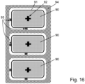
- Fig. 16 shows a detail view of the multi-column embodiment of this kind, showing three BCTs 90 (out of a larger number of BCT devices).
- Each of the BCTs 90 includes one registering structure 92 on a moveable stage 91 ensuring that each BCT can be adjusted in the plane transversal to the beam with the help of piezo elements 93 that are connected to a common frame 94 of the BCT devices.
Landscapes
- Chemical & Material Sciences (AREA)
- Analytical Chemistry (AREA)
- Electron Sources, Ion Sources (AREA)
- Electron Beam Exposure (AREA)
Applications Claiming Priority (1)
| Application Number | Priority Date | Filing Date | Title |
|---|---|---|---|
| EP23160722 | 2023-03-08 |
Publications (1)
| Publication Number | Publication Date |
|---|---|
| EP4428896A1 true EP4428896A1 (en) | 2024-09-11 |
Family
ID=85556577
Family Applications (1)
| Application Number | Title | Priority Date | Filing Date |
|---|---|---|---|
| EP24162043.4A Pending EP4428896A1 (en) | 2023-03-08 | 2024-03-07 | Device and method for calibrating a charged-particle beam |
Country Status (4)
| Country | Link |
|---|---|
| US (1) | US20240304407A1 (enExample) |
| EP (1) | EP4428896A1 (enExample) |
| JP (1) | JP2024127864A (enExample) |
| KR (1) | KR20240137486A (enExample) |
Citations (15)
| Publication number | Priority date | Publication date | Assignee | Title |
|---|---|---|---|---|
| JPH10106931A (ja) * | 1996-10-03 | 1998-04-24 | Hitachi Ltd | 電子ビーム露光方法およびそれを用いた半導体集積回路装置の製造方法 |
| US6222195B1 (en) * | 1996-01-24 | 2001-04-24 | Fujitsu Limited | Charged-particle-beam exposure device and charged-particle-beam exposure method |
| US6768125B2 (en) | 2002-01-17 | 2004-07-27 | Ims Nanofabrication, Gmbh | Maskless particle-beam system for exposing a pattern on a substrate |
| US6858118B2 (en) | 2003-03-21 | 2005-02-22 | Ims-Ionen Mikrofabrikations Systeme Gmbh | Apparatus for enhancing the lifetime of stencil masks |
| US7276714B2 (en) | 2004-04-30 | 2007-10-02 | Ims Nanofabrication Gmbh | Advanced pattern definition for particle-beam processing |
| EP2187427A2 (en) | 2008-11-17 | 2010-05-19 | IMS Nanofabrication AG | Method for maskless particle-beam exposure |
| EP2363875A1 (en) | 2010-03-18 | 2011-09-07 | IMS Nanofabrication AG | Method for multi-beam exposure on a target |
| US8198601B2 (en) | 2009-01-28 | 2012-06-12 | Ims Nanofabrication Ag | Method for producing a multi-beam deflector array device having electrodes |
| US20130143161A1 (en) * | 2011-12-01 | 2013-06-06 | Canon Kabushiki Kaisha | Charged particle beam apparatus |
| US8546767B2 (en) | 2010-02-22 | 2013-10-01 | Ims Nanofabrication Ag | Pattern definition device with multiple multibeam array |
| US9053906B2 (en) | 2013-07-25 | 2015-06-09 | Ims Nanofabrication Ag | Method for charged-particle multi-beam exposure |
| US20170358425A1 (en) * | 2016-06-09 | 2017-12-14 | Nuflare Technology, Inc. | Multi charged-particle beam writing apparatus and adjustment method for the same |
| US20190198290A1 (en) * | 2017-12-26 | 2019-06-27 | Nuflare Technology, Inc. | Multiple charged particle beam writing apparatus, and multiple charged particle beam writing method |
| US10651010B2 (en) | 2018-01-09 | 2020-05-12 | Ims Nanofabrication Gmbh | Non-linear dose- and blur-dependent edge placement correction |
| WO2022192088A1 (en) * | 2021-03-12 | 2022-09-15 | Nikon Corporation | Directed energy beam deflection field monitor and corrector |
-
2024
- 2024-03-05 US US18/596,468 patent/US20240304407A1/en active Pending
- 2024-03-07 KR KR1020240032452A patent/KR20240137486A/ko active Pending
- 2024-03-07 JP JP2024035082A patent/JP2024127864A/ja active Pending
- 2024-03-07 EP EP24162043.4A patent/EP4428896A1/en active Pending
Patent Citations (17)
| Publication number | Priority date | Publication date | Assignee | Title |
|---|---|---|---|---|
| US6222195B1 (en) * | 1996-01-24 | 2001-04-24 | Fujitsu Limited | Charged-particle-beam exposure device and charged-particle-beam exposure method |
| JPH10106931A (ja) * | 1996-10-03 | 1998-04-24 | Hitachi Ltd | 電子ビーム露光方法およびそれを用いた半導体集積回路装置の製造方法 |
| US6768125B2 (en) | 2002-01-17 | 2004-07-27 | Ims Nanofabrication, Gmbh | Maskless particle-beam system for exposing a pattern on a substrate |
| US6858118B2 (en) | 2003-03-21 | 2005-02-22 | Ims-Ionen Mikrofabrikations Systeme Gmbh | Apparatus for enhancing the lifetime of stencil masks |
| US7276714B2 (en) | 2004-04-30 | 2007-10-02 | Ims Nanofabrication Gmbh | Advanced pattern definition for particle-beam processing |
| US8222621B2 (en) | 2008-11-17 | 2012-07-17 | Ims Nanofabrication Ag | Method for maskless particle-beam exposure |
| EP2187427A2 (en) | 2008-11-17 | 2010-05-19 | IMS Nanofabrication AG | Method for maskless particle-beam exposure |
| US8198601B2 (en) | 2009-01-28 | 2012-06-12 | Ims Nanofabrication Ag | Method for producing a multi-beam deflector array device having electrodes |
| US8546767B2 (en) | 2010-02-22 | 2013-10-01 | Ims Nanofabrication Ag | Pattern definition device with multiple multibeam array |
| EP2363875A1 (en) | 2010-03-18 | 2011-09-07 | IMS Nanofabrication AG | Method for multi-beam exposure on a target |
| US8378320B2 (en) | 2010-03-18 | 2013-02-19 | Ims Nanofabrication Ag | Method for multi-beam exposure on a target |
| US20130143161A1 (en) * | 2011-12-01 | 2013-06-06 | Canon Kabushiki Kaisha | Charged particle beam apparatus |
| US9053906B2 (en) | 2013-07-25 | 2015-06-09 | Ims Nanofabrication Ag | Method for charged-particle multi-beam exposure |
| US20170358425A1 (en) * | 2016-06-09 | 2017-12-14 | Nuflare Technology, Inc. | Multi charged-particle beam writing apparatus and adjustment method for the same |
| US20190198290A1 (en) * | 2017-12-26 | 2019-06-27 | Nuflare Technology, Inc. | Multiple charged particle beam writing apparatus, and multiple charged particle beam writing method |
| US10651010B2 (en) | 2018-01-09 | 2020-05-12 | Ims Nanofabrication Gmbh | Non-linear dose- and blur-dependent edge placement correction |
| WO2022192088A1 (en) * | 2021-03-12 | 2022-09-15 | Nikon Corporation | Directed energy beam deflection field monitor and corrector |
Also Published As
| Publication number | Publication date |
|---|---|
| KR20240137486A (ko) | 2024-09-20 |
| US20240304407A1 (en) | 2024-09-12 |
| JP2024127864A (ja) | 2024-09-20 |
Similar Documents
| Publication | Publication Date | Title |
|---|---|---|
| US10410831B2 (en) | Multi-beam writing using inclined exposure stripes | |
| US6903353B2 (en) | Charged particle beam exposure apparatus, device manufacturing method, and charged particle beam applied apparatus | |
| JP4738723B2 (ja) | マルチ荷電粒子線描画装置、荷電粒子線の電流の測定方法及びデバイス製造方法 | |
| NL2003304C2 (en) | Compensation of dose inhomogeneity and image distortion. | |
| US7772574B2 (en) | Pattern lock system for particle-beam exposure apparatus | |
| TWI485745B (zh) | Multi - charged particle beam rendering method and multi - charged particle beam rendering device | |
| US8278635B2 (en) | Global point spreading function in multi-beam patterning | |
| US20020192598A1 (en) | Methods and apparatus for detecting and correcting reticle deformations in microlithography | |
| US6194732B1 (en) | Charged-particle-beam exposure methods with beam parallelism detection and correction | |
| KR20230155971A (ko) | 다중 빔 패턴 정의 장치 | |
| US6352799B1 (en) | Charged-particle-beam pattern-transfer methods and apparatus including beam-drift measurement and correction, and device manufacturing methods comprising same | |
| US6207962B1 (en) | Charged-particle-beam microlithography apparatus and methods exhibiting reduced thermal deformation of mark-defining member | |
| EP4439626A1 (en) | Method for determining focal properties in a target beam field of a multi-beam charged-particle processing apparatus | |
| EP4428896A1 (en) | Device and method for calibrating a charged-particle beam | |
| US6680481B2 (en) | Mark-detection methods and charged-particle-beam microlithography methods and apparatus comprising same | |
| US20150129779A1 (en) | Drawing apparatus, and method of manufacturing article | |
| KR102327865B1 (ko) | 경사진 노출 스트라이프를 사용한 멀티빔 기록 | |
| US20240304413A1 (en) | Optimizing Image Distortion in a Multi Beam Charged Particle Processing Apparatus | |
| US20020036272A1 (en) | Charged-particle-beam microlithography methods and apparatus providing reduced reticle heating | |
| JP7726090B2 (ja) | マルチ荷電粒子ビーム装置の光学系調整方法及びプログラム | |
| JP6376014B2 (ja) | 荷電粒子ビーム描画装置、荷電粒子ビームのビーム分解能測定方法、及び荷電粒子ビーム描画装置の調整方法 | |
| JP3714280B2 (ja) | 電子ビーム近接露光装置における電子ビームの傾き測定方法及び傾き較正方法並びに電子ビーム近接露光装置 | |
| JP2025180659A (ja) | マルチ荷電粒子ビームのビームアレイ補正係数算出方法及びマルチ荷電粒子ビーム描画方法 | |
| JP2025182510A (ja) | マーク位置測定方法、マルチ荷電粒子ビーム描画方法及びマルチ荷電粒子ビーム描画装置 |
Legal Events
| Date | Code | Title | Description |
|---|---|---|---|
| PUAI | Public reference made under article 153(3) epc to a published international application that has entered the european phase |
Free format text: ORIGINAL CODE: 0009012 |
|
| STAA | Information on the status of an ep patent application or granted ep patent |
Free format text: STATUS: THE APPLICATION HAS BEEN PUBLISHED |
|
| AK | Designated contracting states |
Kind code of ref document: A1 Designated state(s): AL AT BE BG CH CY CZ DE DK EE ES FI FR GB GR HR HU IE IS IT LI LT LU LV MC ME MK MT NL NO PL PT RO RS SE SI SK SM TR |
|
| STAA | Information on the status of an ep patent application or granted ep patent |
Free format text: STATUS: REQUEST FOR EXAMINATION WAS MADE |
|
| 17P | Request for examination filed |
Effective date: 20250307 |