EP4428883A2 - Keramischer mehrschichtkondensator - Google Patents
Keramischer mehrschichtkondensator Download PDFInfo
- Publication number
- EP4428883A2 EP4428883A2 EP24161319.9A EP24161319A EP4428883A2 EP 4428883 A2 EP4428883 A2 EP 4428883A2 EP 24161319 A EP24161319 A EP 24161319A EP 4428883 A2 EP4428883 A2 EP 4428883A2
- Authority
- EP
- European Patent Office
- Prior art keywords
- dummy electrode
- electrode
- main body
- length
- ceramic main
- Prior art date
- Legal status (The legal status is an assumption and is not a legal conclusion. Google has not performed a legal analysis and makes no representation as to the accuracy of the status listed.)
- Pending
Links
Images


Classifications
-
- H—ELECTRICITY
- H01—ELECTRIC ELEMENTS
- H01G—CAPACITORS; CAPACITORS, RECTIFIERS, DETECTORS, SWITCHING DEVICES, LIGHT-SENSITIVE OR TEMPERATURE-SENSITIVE DEVICES OF THE ELECTROLYTIC TYPE
- H01G4/00—Fixed capacitors; Processes of their manufacture
- H01G4/002—Details
- H01G4/228—Terminals
- H01G4/232—Terminals electrically connecting two or more layers of a stacked or rolled capacitor
-
- H—ELECTRICITY
- H01—ELECTRIC ELEMENTS
- H01G—CAPACITORS; CAPACITORS, RECTIFIERS, DETECTORS, SWITCHING DEVICES, LIGHT-SENSITIVE OR TEMPERATURE-SENSITIVE DEVICES OF THE ELECTROLYTIC TYPE
- H01G4/00—Fixed capacitors; Processes of their manufacture
- H01G4/002—Details
- H01G4/005—Electrodes
-
- H—ELECTRICITY
- H01—ELECTRIC ELEMENTS
- H01G—CAPACITORS; CAPACITORS, RECTIFIERS, DETECTORS, SWITCHING DEVICES, LIGHT-SENSITIVE OR TEMPERATURE-SENSITIVE DEVICES OF THE ELECTROLYTIC TYPE
- H01G4/00—Fixed capacitors; Processes of their manufacture
- H01G4/002—Details
- H01G4/005—Electrodes
- H01G4/012—Form of non-self-supporting electrodes
-
- H—ELECTRICITY
- H01—ELECTRIC ELEMENTS
- H01G—CAPACITORS; CAPACITORS, RECTIFIERS, DETECTORS, SWITCHING DEVICES, LIGHT-SENSITIVE OR TEMPERATURE-SENSITIVE DEVICES OF THE ELECTROLYTIC TYPE
- H01G4/00—Fixed capacitors; Processes of their manufacture
- H01G4/002—Details
- H01G4/018—Dielectrics
- H01G4/06—Solid dielectrics
- H01G4/08—Inorganic dielectrics
- H01G4/12—Ceramic dielectrics
-
- H—ELECTRICITY
- H01—ELECTRIC ELEMENTS
- H01G—CAPACITORS; CAPACITORS, RECTIFIERS, DETECTORS, SWITCHING DEVICES, LIGHT-SENSITIVE OR TEMPERATURE-SENSITIVE DEVICES OF THE ELECTROLYTIC TYPE
- H01G4/00—Fixed capacitors; Processes of their manufacture
- H01G4/30—Stacked capacitors
-
- H—ELECTRICITY
- H01—ELECTRIC ELEMENTS
- H01G—CAPACITORS; CAPACITORS, RECTIFIERS, DETECTORS, SWITCHING DEVICES, LIGHT-SENSITIVE OR TEMPERATURE-SENSITIVE DEVICES OF THE ELECTROLYTIC TYPE
- H01G2/00—Details of capacitors not covered by a single one of groups H01G4/00-H01G11/00
- H01G2/02—Mountings
- H01G2/06—Mountings specially adapted for mounting on a printed-circuit support
- H01G2/065—Mountings specially adapted for mounting on a printed-circuit support for surface mounting, e.g. chip capacitors
-
- H—ELECTRICITY
- H01—ELECTRIC ELEMENTS
- H01G—CAPACITORS; CAPACITORS, RECTIFIERS, DETECTORS, SWITCHING DEVICES, LIGHT-SENSITIVE OR TEMPERATURE-SENSITIVE DEVICES OF THE ELECTROLYTIC TYPE
- H01G4/00—Fixed capacitors; Processes of their manufacture
- H01G4/002—Details
- H01G4/228—Terminals
- H01G4/232—Terminals electrically connecting two or more layers of a stacked or rolled capacitor
- H01G4/2325—Terminals electrically connecting two or more layers of a stacked or rolled capacitor characterised by the material of the terminals
Definitions
- the present disclosure relates to a multilayer ceramic capacitor.
- Ceramic components which use ceramic materials, include capacitors, inductors, piezoelectric elements, varistors, thermistors, or the like.
- a multilayer ceramic capacitor (MLCC) small in size ensures a high capacity, and is easy to mount. Therefore, the multilayer ceramic capacitor may be used for various electronic devices.
- MLCC multilayer ceramic capacitor
- the multilayer ceramic capacitors may be used for chip-shaped condensers mounted on boards of various electronic products such as imaging devices such as liquid crystal display (LCD) devices, plasma display panel (PDP) devices, and organic light-emitting diodes (OLEDs), computers, personal portable terminals, and smartphones and configured to charge the electronic products with electricity or discharge the electronic products.
- imaging devices such as liquid crystal display (LCD) devices, plasma display panel (PDP) devices, and organic light-emitting diodes (OLEDs)
- LCD liquid crystal display
- PDP plasma display panel
- OLEDs organic light-emitting diodes
- An external electrode may partially cover two opposite end surfaces of a ceramic main body to thin the multilayer ceramic capacitor. However, it may be difficult to implement the thinned multilayer ceramic capacitor when an area in which the external electrode is formed is too large.
- flatness may deteriorate when a level difference is present between an active area and a margin area of the multilayer ceramic capacitor.
- the present disclosure has been made in an effort to provide a multilayer ceramic capacitor that may reduce the likelihood of the occurrence of a flex crack.
- the present disclosure has also been made in an effort to provide a multilayer ceramic capacitor capable of adjusting an area in which an external electrode is formed.
- the present disclosure has also been made in an effort to provide a multilayer ceramic capacitor with improved flatness.
- An embodiment of the present disclosure provides a multilayer ceramic capacitor including: a ceramic main body having a thickness smaller than a width thereof, including: first and second surfaces opposite to each other in a first direction; third and fourth surfaces opposite to each other in a second direction; fifth and sixth surfaces opposite to each other in a third direction; a plurality of dielectric layers; a plurality of first internal electrodes; a plurality of second internal electrodes stacked in the third direction; ; a first external electrode disposed on the first surface of the ceramic main body and connected to the plurality of first internal electrodes; a second external electrode disposed on the second surface of the ceramic main body and connected to the plurality of second internal electrodes; a first cover layer including a first dummy electrode pattern and configured to adjoin an internal electrode closest to the fifth surface among the plurality of first and second internal electrodes; and a second cover layer including a second dummy electrode pattern and configured to adjoin an internal electrode closest to the sixth surface among the plurality of first and second internal electrodes.
- the first dummy electrode pattern may include: a first dummy electrode configured to adjoin the first surface or be drawn out to the first surface; and a second dummy electrode configured to adjoin the second surface or be drawn out to the second surface.
- the ceramic main body may include: an active area that is an area in which the plurality of first internal electrodes and the plurality of second internal electrodes overlap one another in the third direction; a first margin area that is an area between the active area and the first surface of the ceramic main body; and a second margin area that is an area between the active area and the second surface of the ceramic main body, a length L1 of the first dummy electrode may be equal to or larger than a width L2 of the first margin area, and a length L1' of the second dummy electrode may be equal to or larger than a width L2' of the second margin area.
- the second dummy electrode pattern may include: a third dummy electrode configured to adjoin the first surface or be drawn out to the first surface; and a fourth dummy electrode configured to adjoin the second surface or be drawn out to the second surface, a length L3 of the third dummy electrode may be equal to or larger than a width L2 of the first margin area, and a length L3' of the fourth dummy electrode may be equal to or larger than a width L2' of the second margin area.
- the second cover layer may include a first exposed surface, which is a portion of the first surface exposed by the first external electrode, and a second exposed surface, which is a portion of the second surface exposed by the second external electrode
- the second dummy electrode pattern may include: a third dummy electrode spaced apart from the first exposed surface; and a fourth dummy electrode spaced apart from the second exposed surface.
- the second cover layer may include a first exposed surface, which is a portion of the first surface exposed by the first external electrode, and a second exposed surface, which is a portion of the second surface exposed by the second external electrode
- the second dummy electrode pattern may include: a third dummy electrode configured to adjoin the first exposed surface or extended to the first exposed surface; and a fourth dummy electrode configured to adjoin the second exposed surface or extended to the second exposed surface.
- the first dummy electrode pattern may include: a first dummy electrode spaced apart from the first surface; and a second dummy electrode spaced apart from the second surface.
- the second cover layer may include a first exposed surface, which is a portion of the first surface exposed by the first external electrode, and a second exposed surface, which is a portion of the second surface exposed by the second external electrode
- the second dummy electrode pattern may include: a third dummy electrode spaced apart from the first exposed surface; and a fourth dummy electrode spaced apart from the second exposed surface.
- a length L1 of the first dummy electrode may be equal to or larger than a width L2 of the first margin area
- a length L1' of the second dummy electrode may be equal to or larger than a width L2' of the second margin area
- a length L3 of the third dummy electrode may be equal to or larger than the width L2 of the first margin area
- a length L3' of the fourth dummy electrode may be equal to or larger than the width L2' of the second margin area
- the second cover layer may include a first exposed surface, which is a portion of the first surface exposed by the first external electrode, and a second exposed surface, which is a portion of the second surface exposed by the second external electrode
- the second dummy electrode pattern may include: a third dummy electrode configured to adjoin the first exposed surface or be drawn out to the first exposed surface; and a fourth dummy electrode configured to adjoin the second exposed surface or be drawn out to the second exposed surface.
- the second cover layer may include a first exposed surface, which is a portion of the first surface exposed by the first external electrode, and a second exposed surface, which is a portion of the second surface exposed by the second external electrode, a height H1 of the first exposed surface may be smaller than a thickness t of the second cover layer, and a height H2 of the second exposed surface may be smaller than the thickness t of the second cover layer.
- the first external electrode may include a first band portion disposed on the fifth surface of the ceramic main body
- the second external electrode may include a second band portion disposed on the fifth surface of the ceramic main body
- the multilayer ceramic capacitor may further include a first seed electrode layer disposed between the first band portion and the fifth surface, and a second seed electrode layer disposed between the second band portion and the fifth surface.
- a length L1 of the first dummy electrode may be smaller than a length L4 of the first band portion
- a length L1' of the second dummy electrode may be smaller than a length L4' of the second band portion.
- a length L3 of the third dummy electrode may be smaller than a length L4 of the first band portion, and a length L3' of the fourth dummy electrode may be smaller than a length L4' of the second band portion.
- the ceramic main body may include: an active area that is an area in which the plurality of first internal electrodes and the plurality of second internal electrodes overlap one another in the third direction; a first margin area that is an area between the active area and the first surface of the ceramic main body; and a second margin area that is an area between the active area and the second surface of the ceramic main body, a length L1 of the first dummy electrode may be equal to or larger than a width L2 of the first margin area, and a length L1' of the second dummy electrode may be equal to or larger than a width L2' of the second margin area.
- a length L3 of the third dummy electrode may be equal to or larger than the width L2 of the first margin area
- a length L3' of the fourth dummy electrode may be equal to or larger than the width L2' of the second margin area
- At least one of the first dummy electrode, the second dummy electrode, the third dummy electrode, and the fourth dummy electrode may be plural in number.
- the ceramic main body may include: an active area that is an area in which the plurality of first internal electrodes and the plurality of second internal electrodes overlap one another in the third direction; a first margin area that is an area between the active area and the first surface of the ceramic main body; and a second margin area that is an area between the active area and the second surface of the ceramic main body, and a sum S1 of thicknesses of the plurality of first internal electrodes and the plurality of second internal electrodes in the active area may be larger than 0 and equal to or smaller than twice a sum S2 of thicknesses of the first dummy electrode pattern and the second dummy electrode pattern.
- the thickness of the ceramic main body may be larger than 0 and equal to or smaller than 80% of the width.
- the plurality of first internal electrodes and the plurality of second internal electrodes may each have a rectangular shape including first and second long sides facing each other and first and second short sides facing each other when viewed in the third direction, the first short side of the first internal electrode may be connected to the first external electrode, and the first short side of the second internal electrode may be connected to the second external electrode.
- the plurality of first internal electrodes and the plurality of second internal electrodes may each have a rectangular shape including first and second long sides facing each other and first and second short sides facing each other when viewed in the third direction, the first long side of the first internal electrode may be connected to the first external electrode, and the first long side of the second internal electrode may be connected to the second external electrode.
- the multilayer ceramic capacitor according to the embodiment it is possible to suppress the occurrence of the flex crack by disposing the dummy electrode at the portion where stress is concentrated at the time of mounting the multilayer ceramic capacitor on the circuit board.
- the multilayer ceramic capacitor according to the embodiment it is possible to improve the flatness by suppressing the occurrence of the level difference between the active area and the margin area by disposing the dummy electrode in the margin area.
- the multilayer ceramic capacitor according to the embodiment it is possible to adjust an area, in which the external electrode is formed, by plating the external electrode using the end of the internal electrode of the ceramic main body as a seed.
- one component such as a layer, a film, an area, or a plate
- one component can be positioned “directly on” another component, and one component can also be positioned on another component with other components interposed therebetween.
- one component is described as being positioned “directly above” another component, there is no component therebetween.
- the component may be positioned “above” or “below” the reference part, and this configuration does not necessarily mean that the component is positioned “above” or “on” the reference part in a direction opposite to gravity.
- the phrase “in a plan view” means when an object is viewed from above, and the phrase “in a cross-sectional view” means when a cross section made by vertically cutting an object is viewed from a lateral side.
- constituent element when one constituent element is referred to as being “connected to” another constituent element, one constituent element can be “directly connected to” the other constituent element, and one constituent element can also be “indirectly connected to,” “physically connected to,” or “electrically connected to” the other element with other elements therebetween.
- constituent elements are defined as different names according to positions or functions thereof, but the constituent elements may be integrated.
- FIG. 1 is a perspective view schematically illustrating a multilayer ceramic capacitor according to the embodiment
- FIG. 2 is a cross-sectional view taken along line II-II' in FIG. 1
- FIG. 3A is a top plan view schematically illustrating a first internal electrode of the multilayer ceramic capacitor in FIG. 1
- FIG. 3B is a top plan view schematically illustrating a second internal electrode of the multilayer ceramic capacitor in FIG. 1 .
- An L-axis, a W-axis, and a T-axis illustrated in the drawings respectively indicate axes related to a length direction, a width direction, and a thickness direction of the multilayer ceramic capacitor 10.
- the thickness direction (T-axis direction) may be a direction perpendicular to wide surfaces (main surfaces) of constituent elements having sheet shapes.
- the thickness direction (T-axis direction) may be used as the same concept as a direction in which a dielectric layer is stacked.
- the length direction (L-axis direction) may be a direction parallel to the wide surfaces (main surfaces) of the constituent elements having sheet shapes, i.e., a direction intersecting (or orthogonal to) the thickness direction (T-axis direction).
- the length direction (L-axis direction) may be a direction in which the first external electrode 13 and the second external electrode 14 face each other.
- the width direction (W-axis direction) may be a direction parallel to the wide surfaces (main surfaces) of the constituent elements having sheet shapes, i.e., a direction simultaneously intersecting (or orthogonal to) the thickness direction (T-axis direction) and the length direction (L-axis direction).
- the ceramic main body 12 may be formed by stacking a plurality of dielectric layers 124 in the thickness direction (T-axis direction) and then sintering the plurality of dielectric layers 124.
- the plurality of dielectric layers 124 of the ceramic main body 12 which is disposed adjacent to each other, may be integrated with an indistinct boundary therebetween.
- the ceramic main body 12 may have an approximately hexahedral shape having a preset length, width, and thickness along directions with the thickness being smaller than the width.
- the present disclosure is not limited thereto.
- surfaces of the ceramic main body 12, which face each other in the thickness direction (T-axis direction) in which the dielectric layers 124 are stacked, are respectively defined as an upper surface 121 and a lower surface 122.
- surfaces of the ceramic main body 12, which connect the upper surface 121 and the lower surface 122 and face each other in the length direction (L-axis direction) of the ceramic main body 12, are respectively defined as first and second end surfaces 128 and 129.
- Surfaces of the ceramic main body 12, which face each other in the width direction (W-axis direction) perpendicularly intersecting the first and second end surfaces 128 and 129, are respectively defined as first and second lateral surfaces 126 and 127.
- a first direction which is a direction in which the first end surface 128 and the second end surface 129 face each other, may be the length direction (L-axis direction)
- second and third directions which are perpendicular to the first direction and perpendicular to each other, may be respectively the thickness direction (T-axis direction) and the width direction (W-axis direction) or the width direction (W-axis direction) and the thickness direction (T-axis direction).
- a length of the ceramic main body 12 may mean a maximum value among lengths of a plurality of line segments that connects two outermost boundary lines, which are opposite to each other in the length direction (L-axis direction) of the ceramic main body 12 shown in the image of the cross-section, and is parallel to the length direction (L-axis direction).
- the length of the ceramic main body 12 may mean a minimum value among the lengths of the plurality of line segments that connects the two outermost boundary lines, which are opposite to each other in the length direction (L-axis direction) of the ceramic main body 12 shown in the image of the cross-section, and is parallel to the length direction (L-axis direction).
- the length of the ceramic main body 12 may mean an arithmetic mean value of the lengths of at least two line segments among the plurality of line segments that connects the two outermost boundary lines, which are opposite to each other in the length direction (L-axis direction) of the ceramic main body 12 shown in the image of the cross-section, and is parallel to the length direction (L-axis direction).
- a thickness of the ceramic main body 12 may mean a maximum value among the lengths of the plurality of line segments that connects two outermost boundary lines, which are opposite to each other in the thickness direction (T-axis direction) of the ceramic main body 12 shown in the image of the cross-section, and is parallel to the thickness direction (T-axis direction).
- the thickness of the ceramic main body 12 may mean a minimum value among the lengths of the plurality of line segments that connects the two outermost boundary lines, which are opposite to each other in the thickness direction (T-axis direction) of the ceramic main body 12 shown in the image of the cross-section, and is parallel to the thickness direction (T-axis direction).
- the thickness of the ceramic main body 12 may mean an arithmetic mean value of the lengths of at least two line segments among the plurality of line segments that connects the two outermost boundary lines, which are opposite to each other in the thickness direction (T-axis direction) of the ceramic main body 12 shown in the image of the cross-section, and is parallel to the thickness direction (T-axis direction).
- a width of the ceramic main body 12 may mean a maximum value among lengths of a plurality of line segments that connects two outermost boundary lines, which are opposite to each other in the width direction (W-axis direction) of the ceramic main body 12 shown in the image of the cross-section, and is parallel to the width direction (W-axis direction).
- the width of the ceramic main body 12 may mean a minimum value among the lengths of the plurality of line segments that connects the two outermost boundary lines, which are opposite to each other in the width direction (W-axis direction) of the ceramic main body 12 shown in the image of the cross-section, and is parallel to the width direction (W-axis direction).
- the width of the ceramic main body 12 may mean an arithmetic mean value of the lengths of at least two line segments among the plurality of line segments that connects the two outermost boundary lines, which are opposite to each other in the width direction (W-axis direction) of the ceramic main body 12 shown in the image of the cross-section, and is parallel to the width direction (W-axis direction).
- the length, width, and thickness of the ceramic main body 12 may be measured in a micrometer measurement method.
- the micrometer measurement method may be performed by setting a zero point by using a micrometer with Gage R&R (repeatability and reproducibility), inserting the ceramic main body 12 according to the present embodiment between tips of the micrometer, and rotating a measurement lever of the micrometer.
- the length of the ceramic main body 12 may mean a value measured once or an arithmetic mean of values measured multiple times. The same may also apply to the measurement of the width and thickness of the ceramic main body 12.
- a first cover layer 123 having a predetermined thickness may be provided on an upper portion of the internal electrode disposed at an uppermost side in the ceramic main body 12, and a second cover layer 125 may be provided on a lower portion of the internal electrode disposed at a lowermost side in the ceramic main body 12.
- the first cover layer 123 and the second cover layer 125 may have the same composition as the dielectric layer 124 and be formed by stacking one or more dielectric layers respectively on the upper portion of the internal electrode disposed at the uppermost side of the ceramic main body 12 and the lower portion of the internal electrode disposed at the lowermost side of the ceramic main body 12.
- the first dummy electrode pattern 150 may be provided in the first cover layer 123, and the second dummy electrode pattern 160 may be provided in the second cover layer 125.
- the first dummy electrode pattern 150 and the second dummy electrode pattern 160 will be described below in more detail.
- the dielectric layer 124 may include a ceramic material of high dielectric constant.
- the dielectric layer 124 may include a BaTiO 3 (barium titanate)-based ceramic material.
- the BaTiO 3 -based ceramic materials may include (Ba 1-x Ca x ) TiO 3 (0 ⁇ x ⁇ 1), Ba (Ti 1-y Ca y ) O 3 (0 ⁇ y ⁇ 1), (Ba 1-x Ca x ) (Ti 1-y Zr y ) O 3 (0 ⁇ x ⁇ 1, 0 ⁇ y ⁇ 1), Ba (Ti 1-y Zr y ) O 3 (0 ⁇ y ⁇ 1), or the like in which calcium (Ca), zirconium (Zr), or the like are partially dissolved in BaTiOs.
- the present embodiment is not limited thereto.
- the dielectric layer 124 may further include one or more of a ceramic additive, an organic solvent, a plasticizer, a coupling agent, and a dispersant.
- the ceramic additive may be a transition metal oxide or carbide, a rare-earth element, magnesium (Mg), aluminum (Al), or the like.
- the first and second external electrodes 13 and 14 may be plated with conductive metal.
- the conductive metal may include nickel (Ni), copper (Cu), palladium (Pd), gold (Au), or an alloy thereof.
- the present embodiment is not limited thereto.
- the first external electrode 13 is disposed on the first end surface 128 of the ceramic main body 12, and the second external electrode 14 is disposed on the second end surface 129 of the ceramic main body 12.
- the first external electrode 13 includes a first junction portion 133 and a first band portion 135.
- the first junction portion 133 is a portion electrically connected to an exposed end of the first internal electrode 21 while covering a part of the first end surface 128 of the ceramic main body 12.
- the exposed end of the first internal electrode 21 is plated with conductive metal, and the conductive metal is grown not only in the length direction (L-axis direction) but also in the thickness direction (T-axis direction) of the ceramic main body 12, thereby forming the first junction portion 133.
- the conductive metal may be applied to cover only a portion of the second cover layer 125 of the side of the first end surface 128 without covering the entire first end surface 128 of the ceramic main body 12. If the conductive metal is applied to cover the entire first end surface 128, the first external electrode 13 may be grown to the lower surface 122 of the ceramic main body 12, and the multilayer ceramic capacitor 10 may be thickened to that extent, which makes it difficult to implement the thin multilayer ceramic capacitor.
- the first band portion 135 may be a portion extending from the first junction portion 133 to partially cover the upper surface 121, the first lateral surface 126, and the second lateral surface 127 of the ceramic main body 12.
- a first seed electrode layer 137 may be printed between the first band portion 135 and the upper surface 121 of the ceramic main body 12.
- the first seed electrode layer 137 may be plated with conductive metal to form the first band portion 135.
- the first seed electrode layer 137 may be formed by printing a paste containing a conductive metal (e.g., nickel (Ni)). Therefore, the first seed electrode layer 137 may be an area including sintering inhibitors in addition to the conductive metal.
- the first seed electrode layer 137 may be plated with conductive metal to define the first band portion 135. Unlike the first seed electrode layer 137, the first band portion 135 may be an area that rarely contain a component other than the conductive metal.
- the first junction portion 133 may cover a part of the first end surface 128 of the ceramic main body 12.
- the first junction portion 133 may extend downward from an upper end of the first end surface 128 without extending to a lower end of the first end surface 128. That is, there may be a gap between a lower end of the first junction portion 133 and a lower end of the first end surface 128. Therefore, a part of a lower side of the first end surface 128 may be exposed by the first junction portion 133.
- the first end surface 128 may include a first exposed surface 173 that is not covered by the first junction portion 133.
- the second external electrode 14 may include a second junction portion 143 and a second band portion 145.
- the second junction portion 143 may be a portion electrically connected to an exposed end of the second internal electrode 22 while covering a part of the second end surface 129 of the ceramic main body 12.
- the exposed end of the second internal electrode 22 may be plated with conductive metal, and the conductive metal is grown not only in the length direction (L-axis direction) but also in the thickness direction (T-axis direction) of the ceramic main body 12, thereby forming the second junction portion 143.
- the conductive metal may be applied to cover only a portion of the second cover layer 125 side of the second end surface 129 without covering the entire second end surface 129 of the ceramic main body 12. If the conductive metal is applied to cover the entire second end surface 129, the second external electrode 14 may be grown to the lower surface 122 of the ceramic main body 12, and the multilayer ceramic capacitor 10 is thickened to that extent, which makes it difficult to implement the thin multilayer ceramic capacitor.
- the second band portion 145 may be a portion extending from the second junction portion 143 to partially cover the upper surface 121, the first lateral surface 126, and the second lateral surface 127 of the ceramic main body 12.
- a second seed electrode layer 147 may be printed between the second band portion 145 and the upper surface of the ceramic main body 12.
- the second seed electrode layer 147 may be plated with conductive metal to form the second band portion 145.
- the second seed electrode layer 147 may be formed by printing a paste containing a conductive metal (e.g., nickel (Ni)). Therefore, the second seed electrode layer 147 may be an area including sintering inhibitors in addition to the conductive metal.
- the second seed electrode layer 147 may be plated with conductive metal to define the second band portion 145. Unlike the second seed electrode layer 147, the second band portion 145 may be an area that rarely contain a component other than the conductive metal.
- the second junction portion 143 may cover a part of the second end surface 129 of the ceramic main body 12.
- the second junction portion 143 may extend downward from an upper end of the second end surface 129 without extending to a lower end of the second end surface 129. That is, there may be a gap between a lower end of the second junction portion 143 and the lower end of the second end surface 129. Therefore, a part of a lower side of the second end surface 129 may be exposed by the second junction portion 143.
- the second end surface 129 may include a second exposed surface 183 that is not covered by the second junction portion 143.
- the first and second exposed surfaces 173 and 183 may be portions of the second cover layer 125. That is, the first and second exposed surfaces 173 and 183 may be portions of two opposite end surfaces of the second cover layer 125 in the length direction (L-axis direction).
- the second dummy electrode pattern 160 may be provided in the second cover layer 125 which includes the first and second exposed surfaces 173 and 183.
- the second dummy electrode pattern 160 may adjoin the first and second exposed surfaces 173 and 183 or be extended to the first and second exposed surfaces 173 and 183.
- the first dummy electrode pattern 150 and the second dummy electrode pattern 160 will be described below in more detail.
- the plurality of first and second internal electrodes 21 and 22 are alternately stacked with the dielectric layers 124 interposed therebetween.
- the first and second internal electrodes 21 and 22 may be formed and stacked on a ceramic sheet configured to constitute the dielectric layer 124, and then the first and second internal electrodes 21 and 22 may be provided in the ceramic main body 12 and alternately disposed in the thickness direction with the single dielectric layer 124 interposed therebetween by a sintering process.
- the first and second internal electrodes 21 and 22 are electrodes having different polarities.
- the first and second internal electrodes 21 and 22 may be disposed to be opposite to each other in a direction in which the dielectric layers 124 are stacked.
- the first and second internal electrodes 21 and 22 may be electrically insulated from each other by the dielectric layer 124 disposed between the first and second internal electrodes 21 and 22.
- the first and second internal electrodes 21 and 22 are disposed in a staggered manner in the length direction with the dielectric layer 124 interposed therebetween.
- One end of the first internal electrode 21 is exposed through the first end surface 128, and one end of the second internal electrode 22 is exposed through the second end surface 129.
- the end of the first internal electrode 21, which is exposed through the first end surface 128 of the ceramic main body 12 as described above, may be disposed on the first end surface 128 and electrically connected to the first junction portion 133 of the first external electrode 13.
- the end of the second internal electrode 22, which is exposed through the second end surface 129 of the ceramic main body 12, may be disposed on the second end surface 129 and electrically connected to the second junction portion 143 of the second external electrode 14.
- the first internal electrode 21 has a rectangular shape having a pair of long sides A11 and A12 facing each other in the width direction (W-axis direction), and a pair of short sides B11 and B12 facing each other in the length direction (L-axis direction)
- the second internal electrode 22 has a rectangular shape having a pair of long sides A21 and A22 facing each other in the width direction (W-axis direction), and a pair of short sides B21 and B22 facing each other in the length direction (L-axis direction).
- the short side B11 of the first internal electrode 21 contacts one edge of the dielectric layer 124 in the length direction (L-axis direction), and the short side B12 is spaced apart from the opposite edge of the dielectric layer 124 in the length direction (L-axis direction).
- the short side B21 of the second internal electrode 22 is spaced apart from one edge of the dielectric layer 124 in the length direction (L-axis direction), and the short side B22 contacts the opposite edge of the dielectric layer 124 in the length direction (L-axis direction). That is, the first internal electrode 21 and the second internal electrode 22 are disposed to partially overlap each other in the thickness direction (T-axis direction).
- the short side B11 of the first internal electrode 21 is connected to the first external electrode 13, and the short side B22 of the second internal electrode 22 is connected to the second external electrode 14.
- the first external electrode 13 and the second external electrode 14 are respectively disposed on two surfaces of the ceramic main body 12 that face each other in the length direction (L-axis direction).
- first and second internal electrodes 21 and 22 may each be include conductive metal and include nickel (Ni), a nickel (Ni) alloy, or the like, for example.
- Ni nickel
- Ni nickel
- the present embodiment is not limited thereto.
- the capacitance of the multilayer ceramic capacitor 10 is proportional to an overlap area in which the first and second internal electrodes 21 and 22 overlap each other in the direction in which the dielectric layers 124 are stacked.
- external electrodes may be respectively disposed on two surfaces of the ceramic main body that face each other in the width direction (W-axis direction).
- a first internal electrode 21' has a rectangular shape having a pair of long sides A31 and A32 facing each other in the width direction (W-axis direction), and a pair of short sides B31 and B32 facing each other in the length direction (L-axis direction)
- a second internal electrode 22' has a rectangular shape having a pair of long sides A41 and A42 facing each other in the width direction (W-axis direction), and a pair of short sides B41 and B42 facing each other in the length direction (L-axis direction).
- the long side A31 of the first internal electrode 21' may contact one edge of the dielectric layer 124 in the width direction (W-axis direction), and the long side A32 may be spaced apart from the opposite edge of the dielectric layer 124 in the width direction (W-axis direction).
- the long side A41 of the second internal electrode 22' may be spaced apart from one edge of the dielectric layer 124 in the width direction (W-axis direction), and the long side A42 contacts the opposite edge of the dielectric layer 124 in the width direction (W-axis direction). That is, the first internal electrode 21 and the second internal electrode 22 are disposed to partially overlap each other in the thickness direction (T-axis direction).
- the long side A31 of the first internal electrode 21' may be connected to a first external electrode 13'
- the long side A42 of the second internal electrode 22' may be connected to a second external electrode 14'. That is, the first external electrode 13' and the second external electrode 14' are respectively disposed on two surfaces of the ceramic main body 12 that face each other in the width direction (W-axis direction).
- FIG. 5 is a partially enlarged view of FIG. 2
- FIG. 6 is another partially enlarged view of FIG. 2 .
- the two opposite end surfaces of the first cover layer 123 in the length direction (L-axis direction) may be entirely covered by the first and second external electrodes 13 and 14, respectively.
- the two opposite end surfaces of the second cover layer 125 in the length direction (L-axis direction) may be partially covered by the first and second external electrodes 13 and 14 and may have the exposed surfaces 173 and 183.
- the first cover layer 123 may not include an exposed surface. That is, the two opposite end surfaces of the first cover layer 123 in the length direction (L-axis direction) may be covered by the first and second external electrodes 13 and 14.
- the second cover layer 125 may include the first exposed surface 173 and the second exposed surface 183.
- the first exposed surface 173 may be a portion of the first end surface 128 of the ceramic main body 12 that is not covered by the first external electrode 13.
- the second exposed surface 183 may be a portion of the second end surface 129 of the ceramic main body 12 that is not covered by the second external electrode 14.
- the first exposed surface 173 may be a part of the first end surface 128 and may be a surface exposed by the first external electrode 13.
- the second exposed surface 183 may be a part of the second end surface 129 and may be a surface exposed by the second external electrode 14.
- a height H1 of the first exposed surface 173 and a height H2 of the second exposed surface 183 may each be smaller than a thickness t of the second cover layer 125.
- the height H1 of the first exposed surface 173, the height H2 of the second exposed surface 183, and the thickness t of the second cover layer 125 are measured on the basis of an optical microscope or scanning electron microscope (SEM) image of the cross-section (taken in the length direction (L-axis direction) and the thickness direction (T-axis direction)) of the central portion of the multilayer ceramic capacitor 10 in the width direction (W-axis direction).
- SEM scanning electron microscope
- the height H1 of the first exposed surface 173 may be a shortest distance between the lower end of the first junction portion 133 and a straight line parallel to the length direction (L-axis direction) and passing through an outermost point of the lower surface 122 in the thickness direction (T-axis direction) of the ceramic main body 12 shown in the above-mentioned cross-sectional image.
- the height H2 of the second exposed surface 183 may mean a shortest distance between the lower end of the second junction portion 143 and a straight line parallel to the length direction (L-axis direction) and passing through an outermost point of the lower surface 122 in the thickness direction (T-axis direction) of the ceramic main body 12 shown in the above-mentioned cross-sectional image.
- the thickness t of the second cover layer 125 may mean a minimum value of a thickness of the second cover layer 125 shown in the above-mentioned cross-sectional image.
- the height H1 of the first exposed surface 173 may be a distance between an outer peripheral surface of the second cover layer 125 or an imaginary extension surface thereof and an edge adjacent to the second cover layer 125 among the edges of the first junction portion 133.
- the height H2 of the second exposed surface 183 may be a distance between an outer peripheral surface of the second cover layer 125 or an imaginary extension surface thereof and an edge adjacent to the second cover layer 125 among the edges of the second junction portion 143.
- the thickness t of the second cover layer 125 may be a distance between the internal electrode closest to an outer peripheral surface of the second cover layer 125 in the thickness direction of the ceramic main body 12, among the plurality of first and second internal electrodes 21 and 22, and an outer peripheral surface of the second cover layer 125 in the thickness direction of the ceramic main body 12.
- the first external electrode 13 is plated and grown with the first internal electrode 21 as a seed, which is drawn out to the first end surface 128 of the ceramic main body 12.
- the height H1 of the first exposed surface 173 may be smaller than the thickness t of the second cover layer 125.
- the lowermost internal electrode in the thickness direction extends to the first exposed surface 173 but may not be connected to the first junction portion 133 of the first external electrode 13.
- the second external electrode 14 is plated and grown with the second internal electrode as a seed, which is drawn out to the second end surface 129 of the ceramic main body 12.
- the height H2 of the second exposed surface 183 may be smaller than the thickness t of the second cover layer 125.
- the lowermost internal electrode in the thickness direction extends to the second exposed surface 183 but may not be connected to the second junction portion 143 of the second external electrode 14.
- the multilayer ceramic capacitor 10 includes an active area A, a first margin area M1, and a second margin area M2.
- the active area A is an area in which the plurality of first and second internal electrodes 21 and 22 overlaps one another in the thickness direction (T-axis direction) of the ceramic main body 12.
- the first margin area M1 is an area between the active area A and the first end surface 128 of the ceramic main body 12.
- the second margin area M2 is an area between the active area A and the second end surface 129 of the ceramic main body 12.
- the plurality of first and second internal electrodes 21 and 22 overlaps one another in the active area A, the plurality of first internal electrodes 21 is present in the first margin area M1, and the plurality of second internal electrodes 22 is present in the second margin area M2, such that the active area A and the margin areas M1 and M2 may be different in thickness.
- a level difference may be present between the margin areas M1 and M2.
- the multilayer ceramic capacitor cannot have an approximately rectangular parallelepiped shape, which can lead to mountability and reliability issues.
- the ceramic main body 12 is made of a ceramic material and the external electrodes 13 and 14 are made of metal (e.g., nickel (Ni)), the difference in the shrinkage rate of the ceramic and the metal during sintering may cause a stress-concentrating zone in the ceramic main body 12, resulting in bending. When the bending occurs, a crack may be formed when the multilayer ceramic capacitor is mounted on the circuit board.
- metal e.g., nickel (Ni)
- the ceramic main body 12 may have a structure having a thickness smaller than a width.
- the thickness of the ceramic main body 12 may be larger than 0 and equal to or less than 80% of the width. Because the ceramic main body with this structure is relatively thin, there may be a high risk of physical damage such as cracks caused by external impact when the multilayer ceramic capacitor is mounted on the board. Further, if flatness of the ceramic main body is not high, stresses can concentrate on specific locations when the multilayer ceramic capacitor is mounted on the board, which increases a likelihood of fracture. For this reason, electrical characteristics may degrade, and moisture may be highly likely to penetrate through the fractured site.
- the dummy electrode patterns are formed in the margin areas M1 and M2 of the ceramic main body 12, which may improve the flatness by suppressing the occurrence of the level difference, control a difference in shrinkage rate caused during a sintering process, and suppress the occurrence of bending.
- the first dummy electrode pattern 150 is provided in the first cover layer 123. Like the first and second internal electrodes 21 and 22, the first dummy electrode 150 may be formed by printing a conductive paste containing a conductive metal on the dielectric layer 124.
- the first dummy electrode pattern 150 may include at least one first dummy electrode 151 (151a or 151b) and at least one second dummy electrode 152 (152a or 152b).
- the first dummy electrode 151 may adjoin the first end surface 128 or be drawn out to the first end surface 128.
- the second dummy electrode 152 may adjoin the second end surface 129 or be drawn out to the second end surface 129.
- the first dummy electrode 151 may be disposed to extend inward from the first end surface 128 in the length direction of the ceramic main body 12
- the second dummy electrode 152 may be disposed to extend inward from the second end surface 129 in the length direction of the ceramic main body 12.
- a length L1 of the first dummy electrode 151 may be equal to or larger than a width L2 of the first margin area M1.
- L1 means a distance between two opposite ends of the first dummy electrode 151 in the length direction of the ceramic main body 12.
- L2 means a distance between two opposite ends of the first margin area M1 in the length direction of the ceramic main body 12.
- the length L1 of the first dummy electrode 151 is measured on the basis of an optical microscope or scanning electron microscope (SEM) image of the cross-section (taken in the length direction (L-axis direction) and the thickness direction (T-axis direction)) of the central portion of the multilayer ceramic capacitor 10 in the width direction (W-axis direction).
- the length L1 of the first dummy electrode 151 may mean a maximum or minimum value among lengths of a plurality of line segments that connects the two outermost boundary lines, which are opposite to each other in the length direction (L-axis direction) of the first dummy electrode 151 shown in the above-mentioned cross-sectional image, and is parallel to the length direction (L-axis direction).
- the length L1 of the first dummy electrode 151 may mean an arithmetic mean value of the lengths of the above-mentioned plurality of line segments.
- the width L2 of the first margin area M1 may mean an arithmetic mean value of values respectively measured at three points with equivalent intervals on the uppermost portion, three points with equivalent intervals on the intermediate portion, and three points with equivalent intervals on the lowermost portion in the first margin area M1 shown in the above-mentioned cross-sectional image.
- the length L1 of the first dummy electrode 151 is smaller than the width L2 of the first margin area M1, a level difference occurs between the first margin area M1 and the active area A, which may degrade the flatness.
- a length L1' of the second dummy electrode 152 may be equal to or larger than a width L2' of the second margin area M2.
- L1' means a distance between two opposite ends of the second dummy electrode 152 in the length direction of the ceramic main body 12.
- L2' means a distance between two opposite ends of the second margin area M2 in the length direction of the ceramic main body 12.
- the length L1' of the second dummy electrode 152 is measured on the basis of an optical microscope or scanning electron microscope (SEM) image of the cross-section (taken in the length direction (L-axis direction) and the thickness direction (T-axis direction)) of the central portion of the multilayer ceramic capacitor 10 in the width direction (W-axis direction).
- the length L1' of the second dummy electrode 152 may mean a maximum or minimum value among lengths of a plurality of line segments that connects the two outermost boundary lines, which are opposite to each other in the length direction (L-axis direction) of the second dummy electrode 152 shown in the above-mentioned cross-sectional image, and is parallel to the length direction (L-axis direction).
- the length L1' of the second dummy electrode 152 may mean an arithmetic mean value of the lengths of the above-mentioned plurality of line segments.
- the width L2' of the second margin area M2 may mean an arithmetic mean value of values respectively measured at three points with equivalent intervals on the uppermost portion, three points with equivalent intervals on the intermediate portion, and three points with equivalent intervals on the lowermost portion in the second margin area M2 shown in the above-mentioned cross-sectional image.
- the length L1' of the second dummy electrode 152 is smaller than the width L2' of the second margin area M2, a level difference occurs between the second margin area M2 and the active area A, which may degrade the flatness.
- the second dummy electrode pattern 160 is provided in the second cover layer 125.
- the second dummy electrode 160 may be formed by printing a conductive paste containing a conductive metal on the dielectric layer 124.
- the second dummy electrode pattern 160 may include at least one third dummy electrode 161 (161a or 161b) and at least one fourth dummy electrode 162 (162a or 162b).
- the third dummy electrode 161 may adjoin the first exposed surface 173 or be drawn out to the first exposed surface 173.
- the fourth dummy electrode 162 may adjoin the second exposed surface 183 or be drawn out to the second exposed surface 183.
- the third dummy electrode 161 may be disposed to extend inward from the first exposed surface 173 in the length direction (L-axis direction) of the ceramic main body 12
- the fourth dummy electrode 162 may be disposed to extend inward from the second exposed surface 183 in the length direction (L-axis direction) of the ceramic main body 12.
- a length L3 of the third dummy electrode 161 may be equal to or larger than the width L2 of the first margin area M1.
- L3 means a distance between two opposite ends of the third dummy electrode 161 in the length direction of the ceramic main body 12.
- L2 means a distance between two opposite ends of the first margin area M1 in the length direction of the ceramic main body 12.
- the length L3 of the third dummy electrode 153 is measured on the basis of an optical microscope or scanning electron microscope (SEM) image of the cross-section (taken in the length direction (L-axis direction) and the thickness direction (T-axis direction)) of the central portion of the multilayer ceramic capacitor 10 in the width direction (W-axis direction).
- the length L3 of the third dummy electrode 153 may mean a maximum or minimum value among lengths of a plurality of line segments that connects the two outermost boundary lines, which are opposite to each other in the length direction (L-axis direction) of the third dummy electrode 161 shown in the above-mentioned cross-sectional image, and is parallel to the length direction (L-axis direction).
- the length L3 of the third dummy electrode 153 may mean an arithmetic mean value of the lengths of the above-mentioned plurality of line segments.
- the width L2 of the first margin area M1 may mean an arithmetic mean value of values respectively measured at three points with equivalent intervals on the uppermost portion, three points with equivalent intervals on the intermediate portion, and three points with equivalent intervals on the lowermost portion in the first margin area M1 shown in the above-mentioned cross-sectional image.
- the length L3 of the third dummy electrode 161 is smaller than the width L2 of the first margin area M1, a level difference occurs between the first margin area M1 and the active area A, which may degrade the flatness.
- a length L3' of the fourth dummy electrode 162 may be equal to or larger than a width L2' of the second margin area M2.
- L3' means a distance between two opposite ends of the fourth dummy electrode 162 in the length direction of the ceramic main body 12.
- L2' means a distance between two opposite ends of the second margin area M2 in the length direction of the ceramic main body 12.
- the length L3' of the fourth dummy electrode 162 is measured on the basis of an optical microscope or scanning electron microscope (SEM) image of the cross-section (taken in the length direction (L-axis direction) and the thickness direction (T-axis direction)) of the central portion of the multilayer ceramic capacitor 10 in the width direction (W-axis direction).
- the length L3' of the fourth dummy electrode 162 may mean a maximum or minimum value among lengths of a plurality of line segments that connects the two outermost boundary lines, which are opposite to each other in the length direction (L-axis direction) of the fourth dummy electrode 162 shown in the above-mentioned cross-sectional image, and is parallel to the length direction (L-axis direction).
- the length L3' of the fourth dummy electrode 162 may mean an arithmetic mean value of the lengths of the above-mentioned plurality of line segments.
- the width L2' of the second margin area M2 may mean an arithmetic mean value of values respectively measured at three points with equivalent intervals on the uppermost portion, three points with equivalent intervals on the intermediate portion, and three points with equivalent intervals on the lowermost portion in the second margin area M2 shown in the above-mentioned cross-sectional image.
- the length L3' of the fourth dummy electrode 162 is smaller than the width L2' of the second margin area M2, a level difference occurs between the second margin area M2 and the active area A, which may degrade the flatness.
- a sum S1 of thicknesses of the plurality of first internal electrodes 21 and the plurality of second internal electrodes 22 in the active area A may be larger than 0 and equal to or smaller than twice a sum S2 of thicknesses of the first dummy electrode pattern 150 and the second dummy electrode pattern 160. That is, 0 ⁇ S1 ⁇ 2*S2.
- the thickness of the dummy electrode pattern may be determined to compensate for the differences in thickness of the internal electrodes.
- a total sum of the thicknesses of the dummy electrode patterns may be equal to a total sum of the thicknesses of the internal electrodes in the margin areas M1 and M2.
- the thickness of the dummy electrode pattern and the thickness of the internal electrode satisfy the above-mentioned ranges as described above, the occurrence of the level difference caused by the difference in the distribution of the internal electrodes between the active area A and the margin areas M1 and M2 may be minimized or suppressed.
- the first and second dummy electrode patterns 150 and 160 may include the plurality of dummy electrodes. That is, the first dummy electrode pattern 150 may include the plurality of first dummy electrodes 151a and 151b and the plurality of second dummy electrodes 152a and 152b.
- the plurality of first dummy electrodes 151a and 151b may be spaced apart from one another in the thickness direction (T-axis direction), and an interval therebetween may be uniform.
- the plurality of second dummy electrodes 152a and 152b may be spaced apart from one another in the thickness direction (T-axis direction), and an interval therebetween may be uniform.
- the second dummy electrode pattern 160 may include the plurality of third dummy electrodes 161a and 161b and the plurality of fourth dummy electrodes 162a and 162b.
- the plurality of third dummy electrodes 161a and 161b may be spaced apart from one another in the thickness direction (T-axis direction), and an interval therebetween may be uniform.
- the plurality of fourth dummy electrodes 162a and 162b may be spaced apart from one another in the thickness direction (T-axis direction), and an interval therebetween may be uniform.
- the first dummy electrode pattern 150 and the second dummy electrode pattern 160 may each include nickel (Ni), copper (Cu), tin (Sn), palladium (Pd), gold (Au), or an alloy thereof.
- Ni nickel
- Cu copper
- Sn tin
- Pd palladium
- Au gold
- the present disclosure is not limited thereto.
- FIG. 7 is a schematic cross-sectional view illustrating a state in which the multilayer ceramic capacitor illustrated in FIG. 1 is mounted on a board.
- the multilayer ceramic capacitor 10 is connected to first and second electrode pads 211 and 213 provided on an upper surface of a circuit board 200 by means of conductive joining members 215. That is, the multilayer ceramic capacitor 10 may be mounted on the circuit board 200 by means of the first and second electrode pads 211 and 213.
- the first and second electrode pads 211 and 213 may be disposed on the upper surface of the circuit board 200 and spaced apart from each other.
- the first band portion 135 of the first external electrode 13 of the multilayer ceramic capacitor 10 may be fixed to the circuit board 200 by means of the conductive joining member 215 in a state in which the first band portion 135 is disposed to be in contact with the first electrode pad 211.
- the second band portion 145 of the second external electrode 14 may be fixed to the circuit board 200 by means of the conductive joining member 215 in a state in which the second band portion 145 is disposed to be in contact with the second electrode pad 213.
- the multilayer ceramic capacitor 10 may be electrically connected to the first and second electrode pads 211 and 213 of the circuit board 200.
- the conductive joining member 215 may include solder.
- the first external electrode 13 of the multilayer ceramic capacitor 10 may be mounted on the circuit board 200 by being fixed to the first electrode pad 211 by the conductive junction member 215, and the second external electrode 14 is mounted on the circuit board 200 by being fixed to the second electrode pad 213 by the conductive junction member 215.
- the first dummy electrode pattern 150 having the above-mentioned length is disposed on the portion where stresses are concentrated during mounting, which may suppress the occurrence of flex cracks.
- the multilayer ceramic capacitor 10 has the first dummy electrode pattern 150 and the second dummy electrode pattern 160 respectively provided on the first cover layer 123 and the second cover layer 125, the first dummy electrode 151 and the second dummy electrode 152 of the first dummy electrode pattern 150 and the third dummy electrode 161 and the fourth dummy electrode 162 of the second dummy electrode pattern 160 have the above-mentioned thicknesses and lengths.
- the length L1 of the first dummy electrode 151 may be equal to or larger than the width L2 of the first margin area M1
- the length L1' of the second dummy electrode 152 may be equal to or larger than the width L2' of the second margin area M2.
- the length L3 of the third dummy electrode 161 may be equal to or larger than the width L2 of the first margin area M1, and the length L3' of the fourth dummy electrode 162 is equal to or larger than the width L2' of the second margin area M2.
- the multilayer ceramic capacitor 10 according to the present embodiment has the dummy electrode patterns as described above, resistance against stress is high, which makes it possible to prevent the occurrence of the flex cracks even if stress is concentrated on the ends of the band portions 135 and 145 at the time of mounting the multilayer ceramic capacitor 10 on the circuit board 200.
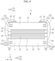
- FIG. 8 is a schematic cross-sectional view illustrating a multilayer ceramic capacitor according to another embodiment
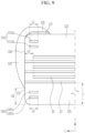
- FIG. 9 is a partially enlarged view of FIG. 8
- FIG. 10 is another partially enlarged view of FIG. 8 .
- the first dummy electrode pattern 1150 may include at least one first dummy electrode 1151 (1151a or 1151b) and at least one second dummy electrode 1152 (1152a or 1152b).
- the first dummy electrode 1151 extends outward from the inside in the length direction of the ceramic main body 12 without reaching the first end surface 128 of the ceramic main body 12
- the second dummy electrode 1152 extends outward from the inside in the length direction of the ceramic main body 12 without reaching the second end surface 129 of the ceramic main body 12. That is, an interval is present between the first dummy electrode 1151 and the first end surface 128 of the ceramic main body 12, and an interval is present between the second dummy electrode 1152 and the second end surface 129 of the ceramic main body 12.
- a length L1 of the first dummy electrode 1151 may be equal to or larger than a width L2 of the first margin area M1.
- L1 means a distance between two opposite ends of the first dummy electrode 1151 in the length direction of the ceramic main body 12.
- L2 means a distance between two opposite ends of the first margin area M1 in the length direction of the ceramic main body 12.
- the length L1 of the first dummy electrode 1151 is measured on the basis of an optical microscope or scanning electron microscope (SEM) image of the cross-section (taken in the length direction (L-axis direction) and the thickness direction (T-axis direction)) of the central portion of the multilayer ceramic capacitor 10 in the width direction (W-axis direction).
- the length L1 of the first dummy electrode 1151 may mean a maximum or minimum value among lengths of a plurality of line segments that connects the two outermost boundary lines, which are opposite to each other in the length direction (L-axis direction) of the first dummy electrode 1151 shown in the above-mentioned cross-sectional image, and is parallel to the length direction (L-axis direction).
- the length L1 of the first dummy electrode 1151 may mean an arithmetic mean value of the lengths of the above-mentioned plurality of line segments.
- the width L2 of the first margin area M1 may mean an arithmetic mean value of values respectively measured at three points with equivalent intervals on the uppermost portion, three points with equivalent intervals on the intermediate portion, and three points with equivalent intervals on the lowermost portion in the first margin area M1 shown in the above-mentioned cross-sectional image.
- a length L1' of the second dummy electrode 1152 may be equal to or larger than a width L2' of the second margin area M2.
- L1' means a distance between two opposite ends of the second dummy electrode 1152 in the length direction of the ceramic main body 12.
- L2' means a distance between two opposite ends of the second margin area M2 in the length direction of the ceramic main body 12.
- the length L1' of the second dummy electrode 1152 is measured on the basis of an optical microscope or scanning electron microscope (SEM) image of the cross-section (taken in the length direction (L-axis direction) and the thickness direction (T-axis direction)) of the central portion of the multilayer ceramic capacitor 10 in the width direction (W-axis direction).
- the length L1' of the second dummy electrode 1152 may mean a maximum or minimum value among lengths of a plurality of line segments that connects the two outermost boundary lines, which are opposite to each other in the length direction (L-axis direction) of the second dummy electrode 1152 shown in the above-mentioned cross-sectional image, and is parallel to the length direction (L-axis direction).
- the length L1' of the second dummy electrode 1152 may mean an arithmetic mean value of the lengths of the above-mentioned plurality of line segments.
- the width L2' of the second margin area M2 may mean an arithmetic mean value of values respectively measured at three points with equivalent intervals on the uppermost portion, three points with equivalent intervals on the intermediate portion, and three points with equivalent intervals on the lowermost portion in the second margin area M2 shown in the above-mentioned cross-sectional image.
- a length L3 of the third dummy electrode 1161 may be equal to or larger than the width L2 of the first margin area M1.
- L3 means a distance between two opposite ends of the third dummy electrode 1161 in the length direction of the ceramic main body 12.
- L2 means a distance between two opposite ends of the first margin area M1 in the length direction of the ceramic main body 12.
- a length L3' of the fourth dummy electrode 1162 may be equal to or larger than a width L2' of the second margin area M2.
- L3' means a distance between two opposite ends of the fourth dummy electrode 1162 in the length direction of the ceramic main body 12.
- L2' means a distance between two opposite ends of the second margin area M2 in the length direction of the ceramic main body 12.
- the length L3 of the third dummy electrode 1161 and the length L3' of the fourth dummy electrode 1162 may be measured in the same way as the length of the first dummy electrode 1151 and the length of the second dummy electrode 1152, a redundant description thereof will be omitted.
- the multilayer ceramic capacitor according to the embodiment illustrated in FIGS. 8 to 10 is identical to the multilayer ceramic capacitor according to the embodiment illustrated in FIGS. 1 to 7 , and a description of the overlapping or identical components will be omitted.
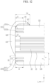
- the first dummy electrode pattern 2150 may include at least one first dummy electrode 2151 (2151a or 2151b) and at least one second dummy electrode 2152 (2152a or 2152b).
- the first dummy electrode 2151 extends outward from the inside in the length direction of the ceramic main body 12 and reaches the first end surface 128 of the ceramic main body 12
- the second dummy electrode 2152 extends outward from the inside in the length direction of the ceramic main body 12 and reaches the second end surface 129 of the ceramic main body 12.
- the first dummy electrode 2151 may adjoin the first end surface 128 of the ceramic main body 12 or be drawn out to the first end surface 128, and the second dummy electrode 2152 may adjoin the second end surface 129 of the ceramic main body 12 or be drawn out to the second end surface 129.
- the first dummy electrode 2151 is disposed to extend inward from the first end surface 128 in the length direction of the ceramic main body 12
- the second dummy electrode 2152 is disposed to extend inward from the second end surface 129 in length direction of the ceramic main body 12.
- the length L1 of the first dummy electrode 2151 may be larger than the width L2 of the first margin area M1.
- L1 means a distance between two opposite ends of the first dummy electrode 2151 in the length direction of the ceramic main body 12.
- L2 means a distance between two opposite ends of the first margin area M1 in the length direction of the ceramic main body 12.
- the length L1 of the first dummy electrode 2151 is measured on the basis of an optical microscope or scanning electron microscope (SEM) image of the cross-section (taken in the length direction (L-axis direction) and the thickness direction (T-axis direction)) of the central portion of the multilayer ceramic capacitor 10 in the width direction (W-axis direction).
- the length L1 of the first dummy electrode 2151 may mean a maximum or minimum value among lengths of a plurality of line segments that connects the two outermost boundary lines, which are opposite to each other in the length direction (L-axis direction) of the first dummy electrode 2151 shown in the above-mentioned cross-sectional image, and is parallel to the length direction (L-axis direction).
- the length L1 of the first dummy electrode 2151 may mean an arithmetic mean value of the lengths of the above-mentioned plurality of line segments.
- the length L4 of the first band portion 135 may mean a shortest distance between a straight line passing through the outermost side point of the first end surface 128 in the length direction (L-axis direction) shown in the above-mentioned cross-section image and the edge opposite to the first end surface 128 of the first band portion 135.
- the width L2 of the first margin area M1 may mean an arithmetic mean value of values respectively measured at three points with equivalent intervals on the uppermost portion, three points with equivalent intervals on the intermediate portion, and three points with equivalent intervals on the lowermost portion in the first margin area M1 shown in the above-mentioned cross-sectional image.
- the length L1' of the second dummy electrode 2152 may be smaller than a length L4' of the second band portion 145.
- L1' means a distance between two opposite ends of the second dummy electrode 2152 in the length direction of the ceramic main body 12
- L4' means a distance between the second end surface 129 of the ceramic main body 12 or an imaginary extension surface thereof and an edge opposite to the second end surface 129 of the ceramic main body 12 among the edges of the second band portion 145.
- the length L1' of the second dummy electrode 2152 may be larger than the width L2' of the second margin area M2.
- L1' means a distance between two opposite ends of the second dummy electrode 2152 in the length direction of the ceramic main body 12.
- L2' means a distance between two opposite ends of the second margin area M2 in the length direction of the ceramic main body 12.
- the length L1' of the second dummy electrode 2152 is measured on the basis of an optical microscope or scanning electron microscope (SEM) image of the cross-section (taken in the length direction (L-axis direction) and the thickness direction (T-axis direction)) of the central portion of the multilayer ceramic capacitor 10 in the width direction (W-axis direction).
- the length L1' of the second dummy electrode 2152 may mean a maximum or minimum value among lengths of a plurality of line segments that connects the two outermost boundary lines, which are opposite to each other in the length direction (L-axis direction) of the second dummy electrode 2152 shown in the above-mentioned cross-section image, and is parallel to the length direction (L-axis direction).
- the length L1' of the second dummy electrode 1152 may mean an arithmetic mean value of the lengths of the above-mentioned plurality of line segments.
- the length L4' of the second band portion 145 may mean a shortest distance between a straight line passing through the outermost side point of the second end surface 129 in the length direction (L-axis direction) shown in the above-mentioned cross-sectional image and the edge opposite to the second end surface 129 of the second band portion 145.
- the width L2' of the second margin area M2 may mean an arithmetic mean value of values respectively measured at three points with equivalent intervals on the uppermost portion, three points with equivalent intervals on the intermediate portion, and three points with equivalent intervals on the lowermost portion in the second margin area M2 shown in the above-mentioned cross-sectional image.
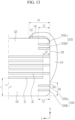
- the second dummy electrode pattern 2160 may include at least one third dummy electrode 2161 (2161a or 2161b) and at least one fourth dummy electrode 2162 (2162a or 2162b).
- the third dummy electrode 2161 extends outward from the inside in the length direction of the ceramic main body 12 and reaches the first exposed surface 173 of the ceramic main body 12. That is, the third dummy electrode 2161 may adjoin the first exposed surface 173 of the ceramic main body 12 or be drawn out to the first exposed surface 173. In other words, the third dummy electrode 2161 may be disposed to extend inward from the first exposed surface 173 in the length direction of the ceramic main body 12.
- the length L3 of the third dummy electrode 2161 may be smaller than the length L4 of the first band portion 135.
- L3 means a distance between two opposite ends of the third dummy electrode 2161 in the length direction of the ceramic main body 12
- L4 means a distance between the first end surface 128 of the ceramic main body 12 or an imaginary extension surface thereof and an edge opposite to the first end surface 128 of the ceramic main body 12 among the edges of the first band portion 135.
- the length L3 of the third dummy electrode 2161 may be larger than the width L2 of the first margin area M1.
- L3 means a distance between two opposite ends of the third dummy electrode 2161 in the length direction of the ceramic main body 12.
- L2 means a distance between two opposite ends of the first margin area M1 in the length direction of the ceramic main body 12.
- the fourth dummy electrode 2162 extends outward from the inside in the length direction of the ceramic main body 12 and reaches the second exposed surface 183 of the ceramic main body 12. That is, the fourth dummy electrode 2162 may adjoin the second exposed surface 183 of the ceramic main body 12 or be drawn out to the second exposed surface 183. In other words, the fourth dummy electrode 2162 may be disposed to extend inward from the second exposed surface 183 in the length direction of the ceramic main body 12.
- the length L3' of the fourth dummy electrode 2162 may be smaller than a length L4' of the second band portion 145.
- L3' means a distance between two opposite ends of the fourth dummy electrode 2162 in the length direction of the ceramic main body 12
- L4' means a distance between the second end surface 129 of the ceramic main body 12 or an imaginary extension surface thereof and an edge opposite to the second end surface 129 of the ceramic main body 12 among the edges of the second band portion 145.
- the length L3' of the fourth dummy electrode 2162 may be larger than the width L2' of the second margin area M2.
- L3' means a distance between two opposite ends of the fourth dummy electrode 2162 in the length direction of the ceramic main body 12.
- L2' means a distance between two opposite ends of the second margin area M2 in the length direction of the ceramic main body 12.
- the length L3 of the third dummy electrode 2161 and the length L3' of the fourth dummy electrode 2162 may be measured in the same way as the length of the first dummy electrode 2151 and the length of the second dummy electrode 2152, a redundant description thereof will be omitted.
- the multilayer ceramic capacitor according to the embodiment illustrated in FIGS. 11 to 13 is identical to the multilayer ceramic capacitor according to the embodiment illustrated in FIGS. 1 to 7 , and a description of the overlapping or identical components will be omitted.
- the first and second dummy electrodes may have the structure illustrated in FIGS. 1 to 7
- the third and fourth dummy electrodes may have the structure illustrated in FIGS. 8 to 10 , and vice versa.
- first and second dummy electrodes may have the structure illustrated in FIGS. 1 to 7
- the third and fourth dummy electrodes may have the structure illustrated in FIGS. 11 to 13 , and vice versa.
- first and second dummy electrodes may have the structure illustrated in FIGS. 8 to 10
- the third and fourth dummy electrodes may have the structure illustrated in FIGS. 11 to 13 , and vice versa.
Landscapes
- Engineering & Computer Science (AREA)
- Power Engineering (AREA)
- Manufacturing & Machinery (AREA)
- Microelectronics & Electronic Packaging (AREA)
- Chemical & Material Sciences (AREA)
- Ceramic Engineering (AREA)
- Inorganic Chemistry (AREA)
- Fixed Capacitors And Capacitor Manufacturing Machines (AREA)
- Ceramic Capacitors (AREA)
Applications Claiming Priority (2)
| Application Number | Priority Date | Filing Date | Title |
|---|---|---|---|
| KR20230031802 | 2023-03-10 | ||
| KR1020230115106A KR20240138444A (ko) | 2023-03-10 | 2023-08-31 | 적층 세라믹 커패시터 |
Publications (2)
| Publication Number | Publication Date |
|---|---|
| EP4428883A2 true EP4428883A2 (de) | 2024-09-11 |
| EP4428883A3 EP4428883A3 (de) | 2025-02-26 |
Family
ID=90361741
Family Applications (1)
| Application Number | Title | Priority Date | Filing Date |
|---|---|---|---|
| EP24161319.9A Pending EP4428883A3 (de) | 2023-03-10 | 2024-03-05 | Keramischer mehrschichtkondensator |
Country Status (3)
| Country | Link |
|---|---|
| US (1) | US12525396B2 (de) |
| EP (1) | EP4428883A3 (de) |
| JP (1) | JP2024128940A (de) |
Family Cites Families (20)
| Publication number | Priority date | Publication date | Assignee | Title |
|---|---|---|---|---|
| KR20050093879A (ko) | 2004-03-19 | 2005-09-23 | 삼성전기주식회사 | 보강패턴을 갖는 적층 세라믹 콘덴서 |
| US8120891B2 (en) * | 2007-12-17 | 2012-02-21 | Murata Manufacturing Co., Ltd. | Multilayer capacitor having low equivalent series inductance and controlled equivalent series resistance |
| US8194391B2 (en) * | 2007-12-21 | 2012-06-05 | Murata Manufacturing Co., Ltd. | Multilayer ceramic electronic component and manufacturing method thereof |
| JP5672162B2 (ja) * | 2010-07-21 | 2015-02-18 | 株式会社村田製作所 | 電子部品 |
| JP5736982B2 (ja) | 2010-07-21 | 2015-06-17 | 株式会社村田製作所 | セラミック電子部品 |
| JP5532027B2 (ja) | 2010-09-28 | 2014-06-25 | 株式会社村田製作所 | 積層セラミック電子部品およびその製造方法 |
| JP5482763B2 (ja) | 2011-10-24 | 2014-05-07 | 株式会社村田製作所 | 電子部品 |
| KR101565651B1 (ko) * | 2013-10-08 | 2015-11-03 | 삼성전기주식회사 | 적층 세라믹 커패시터 및 그 실장 기판 |
| KR102089694B1 (ko) | 2014-04-30 | 2020-03-16 | 삼성전기주식회사 | 적층 세라믹 전자부품 |
| US9627136B2 (en) * | 2014-09-30 | 2017-04-18 | Murata Manufacturing Co., Ltd. | Multilayer ceramic capacitor |
| US11443898B2 (en) * | 2017-04-10 | 2022-09-13 | Presidio Components. Inc. | Multilayer broadband ceramic capacitor with internal air gap capacitance |
| KR20190059008A (ko) * | 2017-11-22 | 2019-05-30 | 삼성전기주식회사 | 적층 세라믹 커패시터 |
| JP7107712B2 (ja) * | 2018-03-19 | 2022-07-27 | 太陽誘電株式会社 | セラミック電子部品およびその製造方法 |
| US11069479B2 (en) * | 2018-07-19 | 2021-07-20 | Samsung Electro-Mechanics Co., Ltd. | Multilayer capacitor |
| KR102191250B1 (ko) * | 2018-10-10 | 2020-12-15 | 삼성전기주식회사 | 적층 세라믹 전자부품 |
| US11037733B2 (en) | 2018-10-11 | 2021-06-15 | Samsung Electro-Mechanics Co., Ltd. | Multilayer ceramic capacitor having dummy pattern |
| CN111199830B (zh) | 2018-10-30 | 2021-11-30 | Tdk株式会社 | 层叠陶瓷电子部件 |
| JP7514069B2 (ja) | 2018-10-30 | 2024-07-10 | Tdk株式会社 | 積層セラミック電子部品 |
| KR20240138286A (ko) | 2023-03-10 | 2024-09-20 | 삼성전기주식회사 | 적층 세라믹 커패시터 |
| KR20240148055A (ko) | 2023-04-03 | 2024-10-11 | 삼성전기주식회사 | 적층 세라믹 커패시터 |
-
2024
- 2024-01-15 JP JP2024004051A patent/JP2024128940A/ja active Pending
- 2024-01-22 US US18/419,026 patent/US12525396B2/en active Active
- 2024-03-05 EP EP24161319.9A patent/EP4428883A3/de active Pending
Also Published As
| Publication number | Publication date |
|---|---|
| EP4428883A3 (de) | 2025-02-26 |
| JP2024128940A (ja) | 2024-09-24 |
| US20240304383A1 (en) | 2024-09-12 |
| US12525396B2 (en) | 2026-01-13 |
Similar Documents
| Publication | Publication Date | Title |
|---|---|---|
| JP7779474B2 (ja) | 積層型電子部品 | |
| CN214336569U (zh) | 电容器组件 | |
| US11657966B2 (en) | Multilayer electronic component | |
| KR102122927B1 (ko) | 적층형 커패시터 | |
| KR20140120111A (ko) | 적층 세라믹 커패시터 및 그 제조 방법 | |
| US20240145174A1 (en) | Multilayer electronic component | |
| JP2004235377A (ja) | セラミック電子部品 | |
| EP4428883A2 (de) | Keramischer mehrschichtkondensator | |
| US20250054692A1 (en) | Multilayer electronic component | |
| EP4443450A2 (de) | Keramischer vielschichtkondensator mit blindelektroden in deckschichten | |
| JP2025069920A (ja) | 積層型電子部品 | |
| JP2024079571A (ja) | 積層型電子部品 | |
| KR20240138286A (ko) | 적층 세라믹 커패시터 | |
| KR20240138444A (ko) | 적층 세라믹 커패시터 | |
| CN118629786A (zh) | 多层陶瓷电容器 | |
| US20230215655A1 (en) | Multilayer electronic component | |
| EP4428879A1 (de) | Anschlussrahmen für ein keramisches mehrschichtbauteil | |
| US20230215640A1 (en) | Multilayer electronic component | |
| US20250054693A1 (en) | Multilayer electronic component | |
| US20250210272A1 (en) | Multilayer electronic component | |
| US12387876B2 (en) | Multilayer electronic component | |
| KR20250072095A (ko) | 적층 세라믹 커패시터 | |
| KR20250090555A (ko) | 적층 세라믹 커패시터 | |
| KR20250072094A (ko) | 적층 세라믹 커패시터 | |
| KR20230100594A (ko) | 적층형 전자 부품 |
Legal Events
| Date | Code | Title | Description |
|---|---|---|---|
| PUAI | Public reference made under article 153(3) epc to a published international application that has entered the european phase |
Free format text: ORIGINAL CODE: 0009012 |
|
| STAA | Information on the status of an ep patent application or granted ep patent |
Free format text: STATUS: THE APPLICATION HAS BEEN PUBLISHED |
|
| AK | Designated contracting states |
Kind code of ref document: A2 Designated state(s): AL AT BE BG CH CY CZ DE DK EE ES FI FR GB GR HR HU IE IS IT LI LT LU LV MC ME MK MT NL NO PL PT RO RS SE SI SK SM TR |
|
| PUAL | Search report despatched |
Free format text: ORIGINAL CODE: 0009013 |
|
| AK | Designated contracting states |
Kind code of ref document: A3 Designated state(s): AL AT BE BG CH CY CZ DE DK EE ES FI FR GB GR HR HU IE IS IT LI LT LU LV MC ME MK MT NL NO PL PT RO RS SE SI SK SM TR |
|
| RIC1 | Information provided on ipc code assigned before grant |
Ipc: H01G 2/06 20060101ALN20250121BHEP Ipc: H01G 4/232 20060101ALI20250121BHEP Ipc: H01G 4/012 20060101ALI20250121BHEP Ipc: H01G 4/30 20060101AFI20250121BHEP |
|
| STAA | Information on the status of an ep patent application or granted ep patent |
Free format text: STATUS: REQUEST FOR EXAMINATION WAS MADE |
|
| 17P | Request for examination filed |
Effective date: 20250429 |