EP4428671A1 - Speicherklassenspeicher, datenverarbeitungsverfahren und prozessorsystem - Google Patents
Speicherklassenspeicher, datenverarbeitungsverfahren und prozessorsystem Download PDFInfo
- Publication number
- EP4428671A1 EP4428671A1 EP22906321.9A EP22906321A EP4428671A1 EP 4428671 A1 EP4428671 A1 EP 4428671A1 EP 22906321 A EP22906321 A EP 22906321A EP 4428671 A1 EP4428671 A1 EP 4428671A1
- Authority
- EP
- European Patent Office
- Prior art keywords
- memory
- error correction
- type
- storage class
- memory chip
- Prior art date
- Legal status (The legal status is an assumption and is not a legal conclusion. Google has not performed a legal analysis and makes no representation as to the accuracy of the status listed.)
- Granted
Links
Images


Classifications
-
- G—PHYSICS
- G06—COMPUTING OR CALCULATING; COUNTING
- G06F—ELECTRIC DIGITAL DATA PROCESSING
- G06F3/00—Input arrangements for transferring data to be processed into a form capable of being handled by the computer; Output arrangements for transferring data from processing unit to output unit, e.g. interface arrangements
- G06F3/06—Digital input from, or digital output to, record carriers, e.g. RAID, emulated record carriers or networked record carriers
- G06F3/0601—Interfaces specially adapted for storage systems
- G06F3/0602—Interfaces specially adapted for storage systems specifically adapted to achieve a particular effect
- G06F3/061—Improving I/O performance
-
- G—PHYSICS
- G06—COMPUTING OR CALCULATING; COUNTING
- G06F—ELECTRIC DIGITAL DATA PROCESSING
- G06F11/00—Error detection; Error correction; Monitoring
- G06F11/07—Responding to the occurrence of a fault, e.g. fault tolerance
- G06F11/08—Error detection or correction by redundancy in data representation, e.g. by using checking codes
- G06F11/10—Adding special bits or symbols to the coded information, e.g. parity check, casting out 9's or 11's
- G06F11/1008—Adding special bits or symbols to the coded information, e.g. parity check, casting out 9's or 11's in individual solid state devices
- G06F11/1072—Adding special bits or symbols to the coded information, e.g. parity check, casting out 9's or 11's in individual solid state devices in multilevel memories
-
- G—PHYSICS
- G06—COMPUTING OR CALCULATING; COUNTING
- G06F—ELECTRIC DIGITAL DATA PROCESSING
- G06F11/00—Error detection; Error correction; Monitoring
- G06F11/07—Responding to the occurrence of a fault, e.g. fault tolerance
- G06F11/08—Error detection or correction by redundancy in data representation, e.g. by using checking codes
- G06F11/10—Adding special bits or symbols to the coded information, e.g. parity check, casting out 9's or 11's
- G06F11/1008—Adding special bits or symbols to the coded information, e.g. parity check, casting out 9's or 11's in individual solid state devices
- G06F11/1012—Adding special bits or symbols to the coded information, e.g. parity check, casting out 9's or 11's in individual solid state devices using codes or arrangements adapted for a specific type of error
-
- G—PHYSICS
- G06—COMPUTING OR CALCULATING; COUNTING
- G06F—ELECTRIC DIGITAL DATA PROCESSING
- G06F3/00—Input arrangements for transferring data to be processed into a form capable of being handled by the computer; Output arrangements for transferring data from processing unit to output unit, e.g. interface arrangements
- G06F3/06—Digital input from, or digital output to, record carriers, e.g. RAID, emulated record carriers or networked record carriers
- G06F3/0601—Interfaces specially adapted for storage systems
- G06F3/0602—Interfaces specially adapted for storage systems specifically adapted to achieve a particular effect
- G06F3/0614—Improving the reliability of storage systems
-
- G—PHYSICS
- G06—COMPUTING OR CALCULATING; COUNTING
- G06F—ELECTRIC DIGITAL DATA PROCESSING
- G06F3/00—Input arrangements for transferring data to be processed into a form capable of being handled by the computer; Output arrangements for transferring data from processing unit to output unit, e.g. interface arrangements
- G06F3/06—Digital input from, or digital output to, record carriers, e.g. RAID, emulated record carriers or networked record carriers
- G06F3/0601—Interfaces specially adapted for storage systems
- G06F3/0628—Interfaces specially adapted for storage systems making use of a particular technique
- G06F3/0629—Configuration or reconfiguration of storage systems
-
- G—PHYSICS
- G06—COMPUTING OR CALCULATING; COUNTING
- G06F—ELECTRIC DIGITAL DATA PROCESSING
- G06F3/00—Input arrangements for transferring data to be processed into a form capable of being handled by the computer; Output arrangements for transferring data from processing unit to output unit, e.g. interface arrangements
- G06F3/06—Digital input from, or digital output to, record carriers, e.g. RAID, emulated record carriers or networked record carriers
- G06F3/0601—Interfaces specially adapted for storage systems
- G06F3/0668—Interfaces specially adapted for storage systems adopting a particular infrastructure
- G06F3/0671—In-line storage system
-
- G—PHYSICS
- G06—COMPUTING OR CALCULATING; COUNTING
- G06F—ELECTRIC DIGITAL DATA PROCESSING
- G06F2212/00—Indexing scheme relating to accessing, addressing or allocation within memory systems or architectures
- G06F2212/10—Providing a specific technical effect
- G06F2212/1016—Performance improvement
-
- G—PHYSICS
- G06—COMPUTING OR CALCULATING; COUNTING
- G06F—ELECTRIC DIGITAL DATA PROCESSING
- G06F2212/00—Indexing scheme relating to accessing, addressing or allocation within memory systems or architectures
- G06F2212/10—Providing a specific technical effect
- G06F2212/1032—Reliability improvement, data loss prevention, degraded operation etc
-
- Y—GENERAL TAGGING OF NEW TECHNOLOGICAL DEVELOPMENTS; GENERAL TAGGING OF CROSS-SECTIONAL TECHNOLOGIES SPANNING OVER SEVERAL SECTIONS OF THE IPC; TECHNICAL SUBJECTS COVERED BY FORMER USPC CROSS-REFERENCE ART COLLECTIONS [XRACs] AND DIGESTS
- Y02—TECHNOLOGIES OR APPLICATIONS FOR MITIGATION OR ADAPTATION AGAINST CLIMATE CHANGE
- Y02D—CLIMATE CHANGE MITIGATION TECHNOLOGIES IN INFORMATION AND COMMUNICATION TECHNOLOGIES [ICT], I.E. INFORMATION AND COMMUNICATION TECHNOLOGIES AIMING AT THE REDUCTION OF THEIR OWN ENERGY USE
- Y02D10/00—Energy efficient computing, e.g. low power processors, power management or thermal management
Definitions
- This application relates to the computer field, and in particular, to a storage class memory, a data processing method, and a processor system.
- a storage class memory (storage class memory, SCM) is a new type of storage medium whose storage capacity, access speed, and costs are between those of a main memory (for example, a dynamic random access memory (Dynamic Random Access Memory, DRAM)) and a hard disk (for example, a NAND flash (NAND flash)).
- a main memory for example, a dynamic random access memory (Dynamic Random Access Memory, DRAM)
- a hard disk for example, a NAND flash (NAND flash)
- DRAM dynamic random access memory
- NAND flash NAND flash
- the SCM has a persistence capability, prevents data loss after a power failure, and has a larger storage capacity.
- the SCM has a faster access speed.
- the SCM implements memory error correction based on a built-in controller. Because a storage medium in the controller may cache data, an access latency of the SCM is uncertain, the SCM cannot be compatible with a double data rate (Double Data Rate, DDR) protocol, and universality of the SCM is low. Therefore, how to improve reliability of the SCM and minimize the access latency of the SCM when the SCM is compatible with the DDR protocol is an urgent problem to be resolved currently.
- DDR Double Data Rate
- This application provides a storage class memory, a data processing method, and a processor system, so that reliability of the SCM can be improved and an access latency of the SCM can be minimized when the SCM is compatible with a DDR protocol.
- a storage class memory is provided.
- a plurality of memory chips included in the storage class memory are divided into at least one group, each group of the at least one group includes a first-type memory chip and a second-type memory chip.
- the second-type memory chip is configured to store running error correction code
- the first-type memory chip is configured to store data and retry error correction code.
- the running error correction code is for performing first-level memory error correction on data stored in the first-type memory chip in the same group.
- the retry error correction code is for performing, when the first-level memory error correction fails, second-level memory error correction on the data stored in the first-type memory chip.
- a two-level memory error correction mechanism is used to ensure high reliability of data stored in the storage class memory and minimize an access latency.
- the two-level memory error correction mechanism is used in this embodiment of this application.
- an error rate of the storage class memory is low, the high reliability of the data stored in the storage class memory can be ensured by using the first-level memory error correction, and the access latency is effectively shortened.
- the error rate of the storage class memory is high, the high reliability of the data stored in the storage class memory can also be ensured by using the second-level memory error correction, and the access latency is shortened in combination with the first-level memory error correction.
- memory chips of the storage class memory are arranged, so that a bit width of the storage class memory meets a memory bit width indicated by a double data rate (Double Data Rate, DDR) protocol.
- DDR Double Data Rate
- the storage class memory is compatible with the DDR protocol, the storage class memory can be connected to more types of processors (processors), and universality of the storage class memory is improved.
- a quantity of first-type memory chips and a quantity of second-type memory chips in each group are determined based on a bit width of the first-type memory chip, a bit width of the second-type memory chip, and the memory bit width indicated by the DDR protocol.
- the memory bit width indicated by the DDR protocol is 80 bits (bits)
- both the bit width of the first-type memory chip and the bit width of the second-type memory chip are 8 bits
- 10 memory chips included in the storage class memory are divided into two groups.
- Each group includes four first-type memory chips and one second-type memory chip.
- a sum of bit widths of the four first-type memory chips and the second-type memory chip included in each group is 40 bits
- a unit data access amount of each bit is 16 bytes (bytes) or 32 bytes.
- the first-type memory chip includes M first-type banks and N second-type banks.
- the first-type bank is configured to store data.
- the second-type bank is configured to store the retry error correction code. Therefore, a memory controller or firmware (firmware, FW) can perform online switching or upgrade on a quantity of first-type banks and a quantity of second-type banks based on a usage scenario, to improve flexibility to adapt to reliability requirements of different systems.
- a unit data access amount of the first-type bank and a unit data access amount of the second-type bank each are a unit data access amount of one bit in the bit width of the first-type memory chip. Therefore, a unit data access amount of the storage class memory meets a length of a cache line (cache line) of the processor connected to the storage class memory, to improve the universality of the storage class memory.
- the first-type memory chip further includes a third-type bank.
- the third-type bank is configured to implement a function of performing bad block management on a bank of the first-type memory chip. Therefore, space of the storage class memory is saved, the storage class memory is more easily compatible with a memory (such as a DRAM) that meets the DDR protocol, and the universality of the storage class memory is improved.
- a data processing method is provided.
- the method is executed by a controller, and the controller is connected to the storage class memory in the first aspect or any possible one in the first aspect and a processor.
- the method includes: The controller performs first-level memory error correction on data stored in a first-type memory chip in a same group in the storage class memory. When the first-level memory error correction fails, the controller obtains each first-type memory chip, and performs second-level memory error correction on data stored in the first-type memory chip.
- that the controller performs first-level memory error correction on the data stored in the first-type memory chip in the same group in the storage class memory includes: The controller performs, by using hamming code or block code, first-level memory error correction on the data stored in the first-type memory chip in the same group in the storage class memory. The controller performs first-level memory error correction on a single bit in 128 bytes to 512 bytes of the data stored in the first-type memory chip in the same group in the storage class memory.
- the controller performs second-level memory error correction on the data stored in the first-type memory chip includes: The controller performs, by using block code or low-density parity-check code, second-level memory error correction on the data stored in the first-type memory chip. The controller performs second-level memory error correction on hundreds of bits in 2048 bytes to 4096 bytes of the data stored in the first-type memory chip.
- the method further includes: The controller converts instructions of the processor into instructions of the storage class memory, and converts the instructions of the storage class memory into instructions of the processor. Therefore, the processor performs a read/write operation on the storage class memory.
- a processor system includes a controller, the storage class memory in the first aspect or any possible one in the first aspect, and a processor.
- the controller is separately connected to the processor and at least one storage class memory.
- the controller is configured to perform an operation step of the method in the second aspect or any possible one in the second aspect.
- This application may further combine the implementations provided in the foregoing aspects to provide more implementations.
- a smallest data unit is a bit (bit), and the bit is also a smallest data unit of a memory (or main memory).
- a value of one bit is "0" or "1”, and eight consecutive bits form one byte (byte).
- the byte represents a letter or a number.
- a value of a single bit stored in the memory may change due to an electric field, a magnetic field, or even cosmic ray interference. If a value of a single bit in a byte that is important for system operation changes, a system error may occur, resulting in system breakdown or another fault.
- Error correcting code is a technology that can implement error checking and error correction.
- An error-correcting code memory is a memory to which the ECC technology is applied, in other words, is a memory that can implement error checking and error correction.
- the error-correcting code memory is widely used in a server and a graphics workstation, so that stability and reliability of computer operation can be improved.
- Embodiments of this application provide a storage class memory, and in particular, provide a storage class memory with high reliability and a low latency.
- a two-level memory error correction mechanism is used to ensure high reliability of data stored in the storage class memory and minimize an access latency.
- memory chips of the storage class memory are arranged, so that a bit width of the storage class memory meets a memory bit width indicated by a double data rate (Double Data Rate, DDR) protocol.
- DDR Double Data Rate
- the storage class memory is compatible with the DDR protocol
- the storage class memory can be connected to more types of processors (processors), and universality of the storage class memory is improved.
- the memory chip may be a phase change memory (Phase Change Memory, PCM).
- the phase change memory is a storage apparatus that stores data by using an electrical conductivity difference shown when a special material (for example, chalcogenide) is converted between a crystalline state and an amorphous state.
- the memory bit width refers to an amount of data that can be transmitted by a memory at a time. A larger bit width indicates a larger amount of data to be transmitted at a time.
- the memory bit width may also be referred to as a data bit width, or referred to as a bit width for short.
- a plurality of memory chips included in the storage class memory are divided into at least one group.
- Each of the at least one group includes a first-type memory chip and a second-type memory chip. It may be understood that the at least one group refers to at least one channel (channel) of a DDR.
- a quantity of first-type memory chips and a quantity of second-type memory chips in each group are determined based on a bit width of the first-type memory chip, a bit width of the second-type memory chip, and the memory bit width indicated by the DDR protocol, so that the bit width of the storage class memory meets the memory bit width indicated by the DDR protocol.
- the second-type memory chip is configured to store running error correction code.
- the running error correction code is for performing first-level memory error correction on data stored in the first-type memory chip in the same group. It should be understood that the running error correction code may be generated based on the data stored in the first-type memory chip that belongs to the same group.
- the first-level memory error correction refers to performing memory error correction on the data stored in the first-type memory chip that belongs to the same group.
- running error correction code stored in a second-type memory chip included in the 1 st group is generated based on the data stored in the first-type memory chip included in the 1 st group.
- the running error correction code stored in the second-type memory chip included in the 1 st group is for performing first-level memory error correction on the data stored in the first-type memory chip included in the 1 st group.
- the first-type memory chip is configured to store data and retry error correction code.
- the retry error correction code is for performing, when the first-level memory error correction fails, second-level memory error correction on the data stored in the first-type memory chip. It should be understood that the retry error correction code may be generated based on the data stored in the first-type memory chip.
- the second-level memory error correction refers to performing memory error correction on data stored in each first-type memory chip. For example, retry error correction code stored in a first-type memory chip included in the 1 st group is generated based on data stored in the same first-type memory chip.
- the retry error correction code stored in the first-type memory chip included in the 1 st group is for performing second-level memory error correction on the data stored in the same first-type memory chip.
- the running error correction code may also be referred to as first-level correction code
- the retry error correction code may also be referred to as second-level correction code
- the first-type memory chip is further configured to implement a function of bad block management on the first-type memory chip.
- disposing a medium for implementing bad block management in the first-type memory chip saves space of the storage class memory, so that the storage class memory is more easily compatible with a memory (such as a DRAM) that meets the DDR protocol, and the universality of the storage class memory is improved.
- the storage class memory may further include another chip, such as a clock chip.
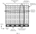
- FIG. 1 is a schematic diagram of a structure of a storage class memory according to an embodiment of this application.
- a storage class memory 100 includes 10 memory chips 110, and a bit width of each memory chip 110 is 8 bits.
- the 10 memory chips 110 are divided into two groups, each group includes five memory chips 110, and a sum of bit widths of the five memory chips 110 included in each group is 40 bits. If a sum of bit widths of the five memory chips 110 included in the two groups is 80 bits, the storage class memory 100 is compatible with the memory bit width of the DDR5.
- the two groups obtained by dividing the 10 memory chips 110 refer to two sub-channels (sub-channels) of the DDR5. This is compatible with a dual-channel standard of the DDR5.
- a bit width of each sub-channel is 40 bits.
- Each group includes four first-type memory chips 111 and one second-type memory chip 112.
- a unit data access amount of each bit in the bit width of the memory chip 110 is 16 bytes or 32 bytes, in other words, each time the storage class memory is accessed, 16B or 32B data may be obtained after a specific latency. If four first-type memory chips 111 are accessed at a time, 64B data can be read or written. If eight first-type memory chips 111 are accessed at a time, 128B data can be read or written. 64B or 128B is equal to a length of a cache line (cache line) of a processor, so that universality of the storage class memory is improved.
- the second-type memory chip 112 is configured to store running error correction code.
- the first-type memory chip 111 is configured to store data and retry error correction code.
- a length of a codeword of the running error correction code is determined by the first-type memory chip 111 and the second-type memory chip 112 in the group. For example, if four first-type memory chips 111 are accessed at a time, 64B data can be read or written, and the length of the codeword of the running error correction code is 64B+16B. If eight first-type memory chips 111 are accessed at a time, 128B data can be read or written, and the length of the codeword of the running error correction code is 128B+32B.
- a length of a codeword of the retry error correction code may be autonomously set by the retry error correction code based on a reliability requirement.
- the storage class memory 100 may be physically divided into a rank (rank) 120, a memory chip (chip) 110, a bank (bank) 130, and a storage cell (cell) 140 in descending order of hierarchies.
- the rank 120 includes all memory chips 110 disposed on the storage class memory 100.
- Each memory chip 110 includes a plurality of banks 130.
- Each bank 130 includes the storage cell 140.
- Each storage cell 140 is determined by a row and a column.
- a medium used by the first-type memory chip 111 to store the retry error correction code may be a part of banks 130 in the plurality of banks 130 included in the first-type memory chip 111.
- the first-type memory chip 111 includes M first-type banks 131 and N second-type banks 132.
- the first-type bank 131 is configured to store data.
- the second-type bank 132 is configured to store the retry error correction code.
- a quantity M of first-type banks 131 and a quantity N of second-type banks 132 may be flexibly configured based on a reliability requirement.
- a memory controller or firmware can switch or upgrade the quantity M of first-type banks 131 and the quantity N of second-type banks 132 online based on a usage scenario, to improve flexibility to adapt to reliability requirements of different systems.
- the first-type memory chip 111 includes 16 banks 130 that can be independently operated.
- the 1 st bank 130 to the 14 th bank 130 serve as the first-type banks 131, and are configured to store data.
- the 15 th bank 130 serves as the second-type bank 132, and is configured to perform second-level memory error correction.
- the 16 th bank 130 in the first-type memory chip 111 serves as a third-type bank 133, and is configured to implement a function of bad block management on the banks 130 of the first-type memory chip 111.
- the faulty bank 130 may be replaced with the 16 th bank 130, to avoid a fault of the storage class memory 100.
- the controller remaps a corresponding address of the 16B to the reserved 16 th bank 130, so that the function of bad block management can be implemented.
- 16B or 32B data may be read or written when the bank 130 is accessed at a time. It is assumed that 16B data may be read or written when the bank 130 is accessed at a time, the length of the codeword of the retry error correction code may be 224B (16*14)+16B. Because the codeword of the retry error correction code is long, an error correction capability of the second-level memory error correction is also strong. This is only one of manners to construct the codeword of the retry error correction code. In some other embodiments, the codeword of the retry error correction code may alternatively be constructed by using data stored in a part of first-type banks 131 in the plurality of first-type banks 131. During the second-level memory error correction, error checking and error correction are cyclically performed on the banks 130 included in the first-type memory chip 111.
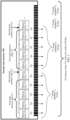
- data on which first-level memory error correction is performed and data on which the second-level memory error correction is performed may form a two-dimensional matrix.
- An x dimension represents four first-type memory chips 111 and one second-type memory chip 112, and a y dimension represents an address of a smallest access unit 16B of a memory chip.
- the four first-type memory chips 111 store data and retry error correction code
- the second-type memory chip 112 stores running error correction code.
- Each row forms a 64B+16B codeword of the running error correction code.
- the entire two-dimensional matrix forms a 512B+208B codeword of the retry error correction code.
- a system After decoding of a codeword of running error correction code in any row fails, a system reads data of the two-dimensional matrix to perform second-level memory error correction, in other words, performs second-level memory error correction on data in each column.
- the system may perform horizontal decoding and vertical decoding in parallel, to effectively reduce an error correction rate of the system.
- the data of the first-type memory chip 111 in each column in the two-dimensional matrix may be data of any eight banks 130 in the 1 st bank 130 to the 14 th bank 130, and the eight banks 130 may be continuous.
- data of a first-type memory chip 111 in the 1 st column may be data of the 1 st bank 130 to the 8 th bank 130
- retry error correction code stored in the first-type memory chip 111 in the 1 st column is generated based on the data of the 1 st bank 130 to the 8 th bank 130.
- the retry error correction code stored in the first-type memory chip 111 in the 1 st column is for performing memory error correction on the data of the 1 st bank 130 to the 8 th bank 130.
- data of a first-type memory chip 111 in the 2 nd column may be data of the 3 rd bank 130 to the 10 th bank 130, and retry error correction code stored in the first-type memory chip 111 in the 2 nd column is generated based on the data of the 3 rd bank 130 to the 10 th bank 130.
- the retry error correction code stored in the first-type memory chip 111 in the 2 nd column is for performing memory error correction on the data of the 3 rd bank 130 to the 10 th bank 130.
- the data of the first-type memory chip 111 for generating the retry error correction code is selected based on a reliability requirement. In other words, if the reliability requirement is high, each column in the two-dimensional matrix includes data of more banks 130. If the reliability requirement is low, each column in the two-dimensional matrix includes data of fewer banks 130.
- the second-type bank 132 in the first-type memory chip 111 may store retry error correction code generated by different first-type banks 131.
- the second-type bank 132 in the first-type memory chip 111 in the 1 st column may store retry error correction code generated based on the data of the 1 st bank 130 to the 8 th bank 130, and retry error correction code generated based on the data of the 3 rd bank 130 to the 10 th bank 130, so that the controller performs memory error correction on data of different first-type banks 131.
- Error correction algorithms used for the first-level memory error correction and the second-level memory error correction include any one of parity-check code, hamming code (hamming code), block code, or error correction code.
- An error correction algorithm used for the first-level memory error correction and an error correction algorithm used for the second-level memory error correction may be the same or different. This is not limited.
- an error correction manner of a DDR5 may be reused in the first-level memory error correction.
- the hamming code or the block code may be used in the first-level memory error correction.
- the memory error correction manner of the DDR5 has a low latency and an error correction capability that can cover most error scenarios of the storage class memory. Therefore, when an error rate of the storage class memory is low, an access latency can be effectively reduced under a condition of high reliability of data stored in the storage class memory.
- the second-level memory error correction may be performed by using retry error correction code in a single or a plurality of first-type memory chips 111.
- the block code or low-density parity-check code may be used in the second-level memory error correction.
- the second-level memory error correction can effectively reduce the error rate of the storage class memory, ensure the high reliability of the data stored in the storage class memory, and prolong a service life of the storage class memory.
- the first-level memory error correction is set between the first-type memory chips 111, in other words, the codeword of the running error correction code is constructed by using data of the first-type memory chips 111 that belong to a same group (channel), and the second-level memory error correction is set in the first-type memory chips 111, in other words, the codeword of the retry error correction code is constructed by using the data of the first-type memory chips 111.
- a two-level memory error correction of the storage class memory may alternatively be set in another manner.
- bit width of a memory chip is 8 bits.
- bit width of the memory chip used by the storage class memory may alternatively be 4 bits.
- a storage class memory 500 includes 20 memory chips 510, and a bit width of each memory chip 510 is 4 bits.
- the 20 memory chips 510 are divided into four groups, each group includes five memory chips 510, and a sum of bit widths of the five memory chips 510 included in each group is 20 bits. If a sum of bit widths of the 20 memory chips 510 included in the four groups is 80 bits, the storage class memory 500 is compatible with a memory bit width of a DDR5.
- Each group includes four first-type memory chips 511 and one second-type memory chip 512.
- the 20 memory chips 510 included in the storage class memory 500 may alternatively be divided into two groups, each group includes 10 memory chips 510, and a sum of bit widths of the 10 memory chips 510 included in each group is 40 bits. If a sum of bit widths of the 20 memory chips 510 included in the two groups is 80 bits, the storage class memory 500 is compatible with the memory bit width of the DDR5.
- Each group includes nine first-type memory chips 511 and one second-type memory chip 512.
- first-type memory chip 511 and the one second-type memory chip 512 For detailed descriptions of the first-type memory chip 511 and the one second-type memory chip 512, refer to the foregoing descriptions of the first-type memory chip 111 and the one second-type memory chip 112.
- the storage class memory When a storage class memory is used as a main memory, the storage class memory may be disposed on a computer device by using a dual-inline-memory-modules (Dual-Inline-Memory-Modules, DIMM) interface, so that a processor of the computer device performs a read/write operation on the storage class memory.
- the computer device may be an independent server or a computing device in a computing cluster.
- a controller further needs to be disposed between the storage class memory and the processor.
- the controller is configured to implement functions such as instruction conversion, memory error correction, bad block management, and address mapping.
- functions such as instruction conversion, memory error correction, bad block management, and address mapping.
- the storage class memory provided in embodiments of this application does not need the built-in controller and the DRAM.
- a memory controller integrated in the processor connected to the storage class memory is used to control the storage class memory, or another external controller is connected between the processor and the storage class memory, to control the storage class memory, ensure a deterministic latency of accessing the storage class memory, and be compatible with the DDR protocol.
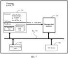
- FIG. 7 is a schematic diagram of a processor system according to an embodiment of this application.
- a processor system 700 includes a controller 710, a storage class memory 720, and a processor 730.
- the processor system 700 may be a computer device, a server, a computing device in a computing cluster, or the like.
- the processor 730 is a computing core and a control core of the processor system 700.
- the processor 730 may be a very large scale integrated circuit.
- An operating system 731 and another software program are disposed in the processor 730, to enable the processor 730 to access the storage class memory 720 and various peripheral component interconnect express (Peripheral Component Interconnect Express, PCIe) devices.
- the processor 730 includes one or more processor cores (cores) 732.
- the processor core 732 in the processor 730 is, for example, a central processing unit (Central Processing unit, CPU) or another application-specific integrated circuit (Application-Specific Integrated Circuit, ASIC).
- CPU Central Processing unit
- ASIC Application-Specific Integrated Circuit
- the processor 730 may alternatively be another general-purpose processor, a digital signal processor (digital signal processor, DSP), an application-specific integrated circuit (application-specific integrated circuit, ASIC), a field programmable gate array (field programmable gate array, FPGA) or another programmable logic device, a discrete gate or a transistor logic device, a discrete hardware component, or the like.
- DSP digital signal processor
- ASIC application-specific integrated circuit
- FPGA field programmable gate array
- the processor system 700 may further include a plurality of processors.
- the processor 730 is configured to write data to the storage class memory 720 or read data from the storage class memory 720.
- the storage class memory 720 may be a main memory of the processor system 700.
- the storage class memory 720 is usually configured to store various types of software that are running in the operating system 731, input and output data, information exchanged with an external memory, and the like.
- the storage class memory 720 needs to have an advantage of a high access speed.
- the processor 730 can access the storage class memory 720 at a high speed by using the controller 710, and perform a read operation and a write operation on any storage cell in the storage class memory 720.
- the controller 710 is a bus circuit controller that controls the storage class memory 720 inside the processor system 700 and that is configured to manage and plan data transmission from the storage class memory 720 to the processor core 732. By using the controller 710, data may be exchanged between the storage class memory 720 and the processor core 732.
- the controller 710 may be integrated into the processor 730, may be built in a northbridge, or may be an independent memory controller chip.
- the controller 710 may be a separate chip, and is connected to the processor core 732 through a system bus.
- a difference from the processor system shown in FIG. 7 lies in that, as shown in FIG. 8 , the controller 710 may be an external controller connected between the storage class memory 720 and the processor 730.
- the external controller may be a centralized controller, and the controller may be connected to a plurality of storage class memories 720, so that a storage capacity of the main memory of the processor system can be expanded, the storage class memory can be more easily compatible with a DDR protocol, to reduce costs of the controller.
- controller 710 may control necessary logic to write data to the storage class memory 720 or read data from the storage class memory 720.
- the controller 710 may be a memory controller in a processor system such as a general-purpose processor, a dedicated accelerator, a GPU, an FPGA, or an embedded processor.
- the processor system 700 further includes various input/output (Input/Output, I/O) devices 740.
- the I/O device 740 is hardware for data transmission, or may be understood as a device connected to an I/O interface. Common I/O devices include a network adapter, a printer, a keyboard, a mouse, and the like. All external memories may also be used as I/O devices, such as hard disks, floppy disks, and optical disks.
- the processor 730, the storage class memory 720, the controller 710, and the I/O device 740 are connected through a bus 750.
- the bus 750 may include a path for transmitting information between the foregoing components (for example, the processor 730 and the storage class memory 720).
- the bus 750 may further include a power bus, a control bus, a status signal bus, and the like. However, for clarity of description, various buses are marked as the bus 750 in the figure.
- the bus 750 may be a PCIe bus, an extended industry standard architecture (extended industry standard architecture, EISA) bus, a unified bus (unified bus, Ubus or UB), a compute express link (compute express link, CXL) bus, a cache coherent interconnect for accelerators (cache coherent interconnect for accelerators, CCIX) bus, or the like.
- the processor 730 may access these I/O devices 740 through a PCIe bus.
- the processor 730 is connected to the storage class memory 720 through a double rate (double data rate, DDR) bus.
- DDR double data rate
- different storage class memories 720 may communicate with the processor 730 through different data buses. Therefore, the DDR bus may be replaced with another type of data bus.
- a type of the bus is not limited in this embodiment of this application.
- the processor system 700 further includes a DPU 760, and the DPU 760 may be connected to the processor 730 through a PCIe bus.
- the DPU 760 offloads applications that are related to artificial intelligence and storage and that are run by another chip (for example, the processor 730) of the processor system 700, to improve data processing performance of the processor system 700, and reduce load of the processor system 700.
- the processor system 700 may further include another dedicated processor.
- the dedicated processor is a processor for a specific application or field, for example, a graphics processing unit (graphics processing unit, GPU) configured to process graphics data or a DSP configured to process signals.
- the processor system 700 may be referred to as a host.
- FIG. 7 is only a schematic diagram.
- the processor system 700 may further include another component, for example, may further include a hard disk, an optical drive, a power supply, a chassis, a heat dissipation system, and another input/output controller and interface, which are not shown in FIG. 7 .
- a quantity of processors, storage class memories, and controllers included in the processor system 700 is not limited in this embodiment of this application.
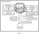
- FIG. 9 is a schematic diagram of a data processing method according to an embodiment of this application.
- a structure shown in FIG. 7 is used as an example for description. It is assumed that the processor 730 writes data to the storage class memory 720 or reads data from the storage class memory 720.
- the data processing method provided in this embodiment of this application includes the following steps.
- the controller 710 performs instruction conversion, in other words, the controller 710 converts a write instruction of the processor 730 into a write instruction that can be recognized by the storage class memory 720.
- S920 The controller 710 generates running error correction code and retry error correction code based on to-be-written data.
- the controller 710 determines a location at which the to-be-written data is written into a first-type memory chip in the storage class memory 720. For example, the controller 710 performs address mapping, in other words, converts a logical block address into a physical block address.
- the logical block address (Logic Block Address, LBA) describes a virtual address of a block in which data on a storage device is located, and is generally used in an auxiliary memory device such as a hard disk.
- the LBA may refer to an address of a data block or a data block to which an address points.
- the physical block address (Physical Block Address, PBA) describes a physical address of a block in which data on a storage device is located.
- mapping relationship between the LBA and the PBA there is a one-to-one mapping relationship between the LBA and the PBA, and the mapping relationship is usually stored in a main memory.
- the mapping relationship between the LBA and the PBA may be stored in the storage class memory.
- the controller 710 generates the running error correction code based on an error correction algorithm (for example, hamming code or block code) by using data that is in the to-be-written data and that is written into first-type memory chips in a same group, and generates the retry error correction code based on an error correction algorithm (for example, block code or low-density parity-check code) by using the data written into the first-type memory chips in the same group.
- an error correction algorithm for example, hamming code or block code
- the controller 710 writes the running error correction code, the retry error correction code, and the to-be-written data into the storage class memory 720.
- the controller 710 performs instruction conversion, in other words, the controller 710 converts a read instruction of the processor 730 into a read instruction that can be recognized by the storage class memory 720.
- the controller 710 reads the data, running error correction code, and retry error correction code from the storage class memory 720.
- the controller 710 determines a storage location of the data in the storage class memory 720, to be specific, first determines a logical block address, and then determines a physical block address of the storage class memory 720 based on the logical block address and a mapping relationship between the LBA and the PBA, to read the data from the storage class memory 720 based on the physical block address.
- the controller 710 performs first-level memory error correction on the read data, in other words, checks the read data by using the running error correction code.
- the controller 710 performs second-level memory error correction, in other words, checks data of a first-type memory chip by using the retry error correction code. For example, the controller 710 performs, by using block code or low-density parity-check code and by using the retry error correction code, second-level memory error correction on the data stored in the first-type memory chip.
- the controller 710 may continuously scan data by using an algorithm (for example, hamming code) algorithm, to check and correct a memory error of each bit.
- an algorithm for example, hamming code
- a method for determining a location at which the controller 710 writes the data to the storage class memory 720 and a location at which the controller 710 reads the data from the storage class memory 720 is not limited in this embodiment of this application.
- a method for generating the running error correction code and the retry error correction code, and a method for checking the read data by using the running error correction code and the retry error correction code may also reuse the conventional technology.
- a computing device includes corresponding hardware structures and/or software modules for performing the functions.
- a person skilled in the art should be easily aware that, in combination with the banks and the method steps in the examples described in embodiments disclosed in this application, this application can be implemented by using hardware or a combination of hardware and computer software. Whether a function is performed by using hardware or hardware driven by computer software depends on a particular application scenario and design constraint condition of the technical solutions.
- the method steps in this embodiment may be implemented in a hardware manner, or may be implemented by executing software instructions by a processor.
- the software instructions may include a corresponding software module.
- the software module may be stored in a random access memory (random access memory, RAM), a flash memory, a read-only memory (read-only memory, ROM), a programmable read-only memory (programmable ROM, PROM), an erasable programmable read-only memory (erasable PROM, EPROM), an electrically erasable programmable read-only memory (electrically EPROM, EEPROM), a register, a hard disk, a removable hard disk, a CD-ROM, or any other form of storage medium well-known in the art.
- a storage medium is coupled to a processor, so that the processor can read information from the storage medium and write information to the storage medium.
- the storage medium may be a component of the processor.
- the processor and the storage medium may be disposed in an ASIC.
- the ASIC may be located in a computing device.
- the processor and the storage medium may alternatively exist as discrete components in a network device or a terminal device.
- All or a part of the foregoing embodiments may be implemented by using software, hardware, firmware, or any combination thereof.
- all or a part of embodiments may be implemented in a form of a computer program product.
- the computer program product includes one or more computer programs and instructions. When the computer programs or instructions are loaded and executed on a computer, all or a part of the processes or functions in embodiments of this application are executed.
- the computer may be a general-purpose computer, a dedicated computer, a computer network, a network device, user equipment, or another programmable apparatus.
- the computer programs or instructions may be stored in a computer-readable storage medium, or may be transmitted from a computer-readable storage medium to another computer-readable storage medium.
- the computer programs or instructions may be transmitted from a website, computer, server, or data center to another website, computer, server, or data center in a wired or wireless manner.
- the computer-readable storage medium may be any usable medium that can be accessed by a computer, or a data storage device, such as a server or a data center, integrating one or more usable media.
- the usable medium may be a magnetic medium, for example, a floppy disk, a hard disk, or a magnetic tape, may be an optical medium, for example, a digital video disc (digital video disc, DVD), or may be a semiconductor medium, for example, a solid-state drive (solid-state drive, SSD).
Landscapes
- Engineering & Computer Science (AREA)
- Theoretical Computer Science (AREA)
- Physics & Mathematics (AREA)
- General Engineering & Computer Science (AREA)
- General Physics & Mathematics (AREA)
- Human Computer Interaction (AREA)
- Quality & Reliability (AREA)
- Techniques For Improving Reliability Of Storages (AREA)
Applications Claiming Priority (3)
| Application Number | Priority Date | Filing Date | Title |
|---|---|---|---|
| CN202111513788 | 2021-12-13 | ||
| CN202210114650.3A CN116263643A (zh) | 2021-12-13 | 2022-01-30 | 存储级内存、数据处理方法和处理器系统 |
| PCT/CN2022/136844 WO2023109571A1 (zh) | 2021-12-13 | 2022-12-06 | 存储级内存、数据处理方法和处理器系统 |
Publications (3)
| Publication Number | Publication Date |
|---|---|
| EP4428671A1 true EP4428671A1 (de) | 2024-09-11 |
| EP4428671A4 EP4428671A4 (de) | 2025-02-26 |
| EP4428671B1 EP4428671B1 (de) | 2025-11-26 |
Family
ID=86722774
Family Applications (1)
| Application Number | Title | Priority Date | Filing Date |
|---|---|---|---|
| EP22906321.9A Active EP4428671B1 (de) | 2021-12-13 | 2022-12-06 | Speicherklassenspeicher, datenverarbeitungsverfahren und prozessorsystem |
Country Status (5)
| Country | Link |
|---|---|
| US (1) | US12602286B2 (de) |
| EP (1) | EP4428671B1 (de) |
| KR (1) | KR20240112955A (de) |
| CN (2) | CN116263643A (de) |
| WO (1) | WO2023109571A1 (de) |
Families Citing this family (4)
| Publication number | Priority date | Publication date | Assignee | Title |
|---|---|---|---|---|
| CN116841795B (zh) * | 2023-08-29 | 2024-01-12 | 苏州浪潮智能科技有限公司 | 一种内存设备控制方法、装置、电子设备及存储介质 |
| CN117971113B (zh) * | 2023-11-30 | 2024-12-03 | 中科驭数(北京)科技有限公司 | 存储阵列的动态资源分配方法、装置、电子设备、介质 |
| CN117971507B (zh) * | 2024-03-29 | 2024-06-21 | 苏州元脑智能科技有限公司 | 一种内存模组及数据存取方法 |
| CN120929420A (zh) * | 2024-05-11 | 2025-11-11 | 华为技术有限公司 | 内存模块、装置和服务器 |
Family Cites Families (15)
| Publication number | Priority date | Publication date | Assignee | Title |
|---|---|---|---|---|
| US20140229655A1 (en) | 2013-02-08 | 2014-08-14 | Seagate Technology Llc | Storing Error Correction Code (ECC) Data In a Multi-Tier Memory Structure |
| US9772900B2 (en) | 2014-07-10 | 2017-09-26 | Samsung Electronics Co., Ltd. | Tiered ECC single-chip and double-chip Chipkill scheme |
| JP6479638B2 (ja) * | 2015-12-09 | 2019-03-06 | 株式会社東芝 | ビデオサーバ装置およびデータ書き込み/読み出し方法 |
| CN107239361B (zh) * | 2016-03-29 | 2019-05-07 | 华为技术有限公司 | 数据处理装置及数据处理方法 |
| CN107516547A (zh) * | 2016-06-16 | 2017-12-26 | 中兴通讯股份有限公司 | 内存硬错误的处理方法及装置 |
| US10229047B2 (en) | 2016-08-06 | 2019-03-12 | Wolley Inc. | Apparatus and method of wear leveling for storage class memory using cache filtering |
| US10579470B1 (en) * | 2018-07-26 | 2020-03-03 | Cadence Design Systems, Inc. | Address failure detection for memory devices having inline storage configurations |
| KR102719499B1 (ko) * | 2018-10-15 | 2024-10-21 | 에스케이하이닉스 주식회사 | 에러 정정 회로, 이를 포함하는 메모리 컨트롤러 및 메모리 시스템 |
| US11061767B2 (en) * | 2019-01-09 | 2021-07-13 | Synopsys, Inc. | Post-ECC CRC for DDR CRC retry performance improvement |
| CN111124741B (zh) * | 2019-12-12 | 2023-02-28 | 上海高性能集成电路设计中心 | 一种面向存储器特征的增强型校验纠错装置 |
| KR20210121654A (ko) | 2020-03-31 | 2021-10-08 | 에스케이하이닉스 주식회사 | 메모리 시스템의 데이터 에러를 복구하는 장치 및 방법 |
| US11170869B1 (en) * | 2020-06-04 | 2021-11-09 | Western Digital Technologies, Inc. | Dual data protection in storage devices |
| TWI732642B (zh) * | 2020-08-03 | 2021-07-01 | 群聯電子股份有限公司 | 資料寫入方法、記憶體控制電路單元以及記憶體儲存裝置 |
| CN111679934B (zh) * | 2020-08-13 | 2020-11-17 | 杭州阿姆科技有限公司 | 基于raid信息的纠错方法、计算机可读存储介质及处理器 |
| US12572417B2 (en) * | 2021-09-23 | 2026-03-10 | Intel Corporation | Translation cache and configurable ECC memory for reducing ECC memory overhead |
-
2022
- 2022-01-30 CN CN202210114650.3A patent/CN116263643A/zh active Pending
- 2022-01-30 CN CN202411165652.0A patent/CN119248182B/zh active Active
- 2022-12-06 KR KR1020247022331A patent/KR20240112955A/ko active Pending
- 2022-12-06 EP EP22906321.9A patent/EP4428671B1/de active Active
- 2022-12-06 WO PCT/CN2022/136844 patent/WO2023109571A1/zh not_active Ceased
-
2024
- 2024-06-11 US US18/740,001 patent/US12602286B2/en active Active
Also Published As
| Publication number | Publication date |
|---|---|
| CN116263643A (zh) | 2023-06-16 |
| WO2023109571A1 (zh) | 2023-06-22 |
| CN119248182B (zh) | 2025-07-08 |
| US12602286B2 (en) | 2026-04-14 |
| CN119248182A (zh) | 2025-01-03 |
| KR20240112955A (ko) | 2024-07-19 |
| US20240330109A1 (en) | 2024-10-03 |
| EP4428671B1 (de) | 2025-11-26 |
| EP4428671A4 (de) | 2025-02-26 |
Similar Documents
| Publication | Publication Date | Title |
|---|---|---|
| EP4428671B1 (de) | Speicherklassenspeicher, datenverarbeitungsverfahren und prozessorsystem | |
| US12181987B2 (en) | HBM RAS cache architecture | |
| US10372339B2 (en) | Extensible memory hub | |
| JP5464528B2 (ja) | 同時読み出し及び書き込みメモリ動作を実行する方法及び装置 | |
| US20230236934A1 (en) | Instant write scheme with dram submodules | |
| US12032443B2 (en) | Shadow DRAM with CRC+RAID architecture, system and method for high RAS feature in a CXL drive | |
| US12498855B2 (en) | Storage system, data storage method, data read method, and storage medium | |
| US20220043605A1 (en) | Memory system, memory system control method, and information processing system | |
| KR20180031572A (ko) | 메모리 장치의 동작 방법, 이를 이용한 메모리 장치 및 그 장치를 포함하는 메모리 시스템 | |
| CN113360323A (zh) | 一种众核计算电路、堆叠芯片和容错控制方法 | |
| CN119149446A (zh) | 一种存储器地址的生成方法、存储控制方法和生成装置 | |
| US11960776B2 (en) | Data protection for stacks of memory dice | |
| CN118502669A (zh) | 数据存储方法、装置及电子设备 | |
| WO2022120586A1 (zh) | 一种存储装置、存储控制装置及片上系统 | |
| CN114077515A (zh) | 数据写入方法、存储器控制电路单元以及存储器存储装置 | |
| WO2025007550A1 (zh) | 一种数据存储方法及相关装置 | |
| WO2024169645A1 (zh) | 一种内存纠错方法、系统及设备 | |
| CN215910890U (zh) | 一种众核计算电路和堆叠芯片 | |
| US11360853B2 (en) | Access method | |
| US12585542B2 (en) | Locked raid with compression for memory interconnect applications having a shared cache line | |
| US12585579B2 (en) | Locked raid with compression for memory interconnect applications | |
| US12461821B2 (en) | Low cost high performance LRAID | |
| TWI829252B (zh) | 低密度奇偶校檢碼的解碼方法及電腦程式產品及裝置 | |
| CN118349482A (zh) | 一种内存管理方法及计算设备 | |
| CN115712518A (zh) | 一种处理内存故障的方法以及相关设备 |
Legal Events
| Date | Code | Title | Description |
|---|---|---|---|
| STAA | Information on the status of an ep patent application or granted ep patent |
Free format text: STATUS: THE INTERNATIONAL PUBLICATION HAS BEEN MADE |
|
| PUAI | Public reference made under article 153(3) epc to a published international application that has entered the european phase |
Free format text: ORIGINAL CODE: 0009012 |
|
| STAA | Information on the status of an ep patent application or granted ep patent |
Free format text: STATUS: REQUEST FOR EXAMINATION WAS MADE |
|
| 17P | Request for examination filed |
Effective date: 20240606 |
|
| AK | Designated contracting states |
Kind code of ref document: A1 Designated state(s): AL AT BE BG CH CY CZ DE DK EE ES FI FR GB GR HR HU IE IS IT LI LT LU LV MC ME MK MT NL NO PL PT RO RS SE SI SK SM TR |
|
| A4 | Supplementary search report drawn up and despatched |
Effective date: 20250129 |
|
| RIC1 | Information provided on ipc code assigned before grant |
Ipc: G06F 11/10 20060101ALI20250123BHEP Ipc: G06F 3/06 20060101AFI20250123BHEP |
|
| DAV | Request for validation of the european patent (deleted) | ||
| DAX | Request for extension of the european patent (deleted) | ||
| GRAP | Despatch of communication of intention to grant a patent |
Free format text: ORIGINAL CODE: EPIDOSNIGR1 |
|
| STAA | Information on the status of an ep patent application or granted ep patent |
Free format text: STATUS: GRANT OF PATENT IS INTENDED |
|
| INTG | Intention to grant announced |
Effective date: 20250731 |
|
| GRAS | Grant fee paid |
Free format text: ORIGINAL CODE: EPIDOSNIGR3 |
|
| GRAA | (expected) grant |
Free format text: ORIGINAL CODE: 0009210 |
|
| STAA | Information on the status of an ep patent application or granted ep patent |
Free format text: STATUS: THE PATENT HAS BEEN GRANTED |
|
| AK | Designated contracting states |
Kind code of ref document: B1 Designated state(s): AL AT BE BG CH CY CZ DE DK EE ES FI FR GB GR HR HU IE IS IT LI LT LU LV MC ME MK MT NL NO PL PT RO RS SE SI SK SM TR |
|
| REG | Reference to a national code |
Ref country code: CH Ref legal event code: F10 Free format text: ST27 STATUS EVENT CODE: U-0-0-F10-F00 (AS PROVIDED BY THE NATIONAL OFFICE) Effective date: 20251126 Ref country code: GB Ref legal event code: FG4D |
|
| REG | Reference to a national code |
Ref country code: DE Ref legal event code: R096 Ref document number: 602022025901 Country of ref document: DE |
|
| REG | Reference to a national code |
Ref country code: IE Ref legal event code: FG4D |
|
| PGFP | Annual fee paid to national office [announced via postgrant information from national office to epo] |
Ref country code: DE Payment date: 20251216 Year of fee payment: 4 |
|
| PGFP | Annual fee paid to national office [announced via postgrant information from national office to epo] |
Ref country code: AT Payment date: 20260113 Year of fee payment: 4 |
|
| REG | Reference to a national code |
Ref country code: NL Ref legal event code: MP Effective date: 20251126 |
|
| PG25 | Lapsed in a contracting state [announced via postgrant information from national office to epo] |
Ref country code: ES Free format text: LAPSE BECAUSE OF FAILURE TO SUBMIT A TRANSLATION OF THE DESCRIPTION OR TO PAY THE FEE WITHIN THE PRESCRIBED TIME-LIMIT Effective date: 20251126 |
|
| REG | Reference to a national code |
Ref country code: LT Ref legal event code: MG9D |
|
| PG25 | Lapsed in a contracting state [announced via postgrant information from national office to epo] |
Ref country code: NO Free format text: LAPSE BECAUSE OF FAILURE TO SUBMIT A TRANSLATION OF THE DESCRIPTION OR TO PAY THE FEE WITHIN THE PRESCRIBED TIME-LIMIT Effective date: 20260226 |
|
| PG25 | Lapsed in a contracting state [announced via postgrant information from national office to epo] |
Ref country code: HR Free format text: LAPSE BECAUSE OF FAILURE TO SUBMIT A TRANSLATION OF THE DESCRIPTION OR TO PAY THE FEE WITHIN THE PRESCRIBED TIME-LIMIT Effective date: 20251126 Ref country code: AT Free format text: LAPSE BECAUSE OF FAILURE TO SUBMIT A TRANSLATION OF THE DESCRIPTION OR TO PAY THE FEE WITHIN THE PRESCRIBED TIME-LIMIT Effective date: 20251126 Ref country code: FI Free format text: LAPSE BECAUSE OF FAILURE TO SUBMIT A TRANSLATION OF THE DESCRIPTION OR TO PAY THE FEE WITHIN THE PRESCRIBED TIME-LIMIT Effective date: 20251126 |
|
| REG | Reference to a national code |
Ref country code: AT Ref legal event code: MK05 Ref document number: 1861713 Country of ref document: AT Kind code of ref document: T Effective date: 20251126 |
|
| PG25 | Lapsed in a contracting state [announced via postgrant information from national office to epo] |
Ref country code: NL Free format text: LAPSE BECAUSE OF FAILURE TO SUBMIT A TRANSLATION OF THE DESCRIPTION OR TO PAY THE FEE WITHIN THE PRESCRIBED TIME-LIMIT Effective date: 20251126 |
|
| PG25 | Lapsed in a contracting state [announced via postgrant information from national office to epo] |
Ref country code: RS Free format text: LAPSE BECAUSE OF FAILURE TO SUBMIT A TRANSLATION OF THE DESCRIPTION OR TO PAY THE FEE WITHIN THE PRESCRIBED TIME-LIMIT Effective date: 20260226 |
|
| PG25 | Lapsed in a contracting state [announced via postgrant information from national office to epo] |
Ref country code: IS Free format text: LAPSE BECAUSE OF FAILURE TO SUBMIT A TRANSLATION OF THE DESCRIPTION OR TO PAY THE FEE WITHIN THE PRESCRIBED TIME-LIMIT Effective date: 20260326 |