EP4425555A1 - Thin film transistor array substrate and manufacturing method therefor - Google Patents
Thin film transistor array substrate and manufacturing method therefor Download PDFInfo
- Publication number
- EP4425555A1 EP4425555A1 EP22887646.2A EP22887646A EP4425555A1 EP 4425555 A1 EP4425555 A1 EP 4425555A1 EP 22887646 A EP22887646 A EP 22887646A EP 4425555 A1 EP4425555 A1 EP 4425555A1
- Authority
- EP
- European Patent Office
- Prior art keywords
- semiconductor layer
- region
- carbon
- substrate
- insulating layer
- Prior art date
- Legal status (The legal status is an assumption and is not a legal conclusion. Google has not performed a legal analysis and makes no representation as to the accuracy of the status listed.)
- Pending
Links
Images






Classifications
-
- H—ELECTRICITY
- H10—SEMICONDUCTOR DEVICES; ELECTRIC SOLID-STATE DEVICES NOT OTHERWISE PROVIDED FOR
- H10D—INORGANIC ELECTRIC SEMICONDUCTOR DEVICES
- H10D30/00—Field-effect transistors [FET]
- H10D30/60—Insulated-gate field-effect transistors [IGFET]
- H10D30/67—Thin-film transistors [TFT]
- H10D30/6704—Thin-film transistors [TFT] having supplementary regions or layers in the thin films or in the insulated bulk substrates for controlling properties of the device
- H10D30/6713—Thin-film transistors [TFT] having supplementary regions or layers in the thin films or in the insulated bulk substrates for controlling properties of the device characterised by the properties of the source or drain regions, e.g. compositions or sectional shapes
-
- H—ELECTRICITY
- H10—SEMICONDUCTOR DEVICES; ELECTRIC SOLID-STATE DEVICES NOT OTHERWISE PROVIDED FOR
- H10D—INORGANIC ELECTRIC SEMICONDUCTOR DEVICES
- H10D86/00—Integrated devices formed in or on insulating or conducting substrates, e.g. formed in silicon-on-insulator [SOI] substrates or on stainless steel or glass substrates
- H10D86/40—Integrated devices formed in or on insulating or conducting substrates, e.g. formed in silicon-on-insulator [SOI] substrates or on stainless steel or glass substrates characterised by multiple TFTs
- H10D86/60—Integrated devices formed in or on insulating or conducting substrates, e.g. formed in silicon-on-insulator [SOI] substrates or on stainless steel or glass substrates characterised by multiple TFTs wherein the TFTs are in active matrices
-
- H—ELECTRICITY
- H10—SEMICONDUCTOR DEVICES; ELECTRIC SOLID-STATE DEVICES NOT OTHERWISE PROVIDED FOR
- H10D—INORGANIC ELECTRIC SEMICONDUCTOR DEVICES
- H10D30/00—Field-effect transistors [FET]
- H10D30/01—Manufacture or treatment
- H10D30/021—Manufacture or treatment of FETs having insulated gates [IGFET]
- H10D30/031—Manufacture or treatment of FETs having insulated gates [IGFET] of thin-film transistors [TFT]
- H10D30/0312—Manufacture or treatment of FETs having insulated gates [IGFET] of thin-film transistors [TFT] characterised by the gate electrodes
- H10D30/0314—Manufacture or treatment of FETs having insulated gates [IGFET] of thin-film transistors [TFT] characterised by the gate electrodes of lateral top-gate TFTs comprising only a single gate
-
- H—ELECTRICITY
- H10—SEMICONDUCTOR DEVICES; ELECTRIC SOLID-STATE DEVICES NOT OTHERWISE PROVIDED FOR
- H10D—INORGANIC ELECTRIC SEMICONDUCTOR DEVICES
- H10D30/00—Field-effect transistors [FET]
- H10D30/01—Manufacture or treatment
- H10D30/021—Manufacture or treatment of FETs having insulated gates [IGFET]
- H10D30/031—Manufacture or treatment of FETs having insulated gates [IGFET] of thin-film transistors [TFT]
- H10D30/0321—Manufacture or treatment of FETs having insulated gates [IGFET] of thin-film transistors [TFT] comprising silicon, e.g. amorphous silicon or polysilicon
-
- H—ELECTRICITY
- H10—SEMICONDUCTOR DEVICES; ELECTRIC SOLID-STATE DEVICES NOT OTHERWISE PROVIDED FOR
- H10D—INORGANIC ELECTRIC SEMICONDUCTOR DEVICES
- H10D30/00—Field-effect transistors [FET]
- H10D30/60—Insulated-gate field-effect transistors [IGFET]
- H10D30/67—Thin-film transistors [TFT]
- H10D30/6729—Thin-film transistors [TFT] characterised by the electrodes
- H10D30/673—Thin-film transistors [TFT] characterised by the electrodes characterised by the shapes, relative sizes or dispositions of the gate electrodes
- H10D30/6731—Top-gate only TFTs
-
- H—ELECTRICITY
- H10—SEMICONDUCTOR DEVICES; ELECTRIC SOLID-STATE DEVICES NOT OTHERWISE PROVIDED FOR
- H10D—INORGANIC ELECTRIC SEMICONDUCTOR DEVICES
- H10D30/00—Field-effect transistors [FET]
- H10D30/60—Insulated-gate field-effect transistors [IGFET]
- H10D30/67—Thin-film transistors [TFT]
- H10D30/674—Thin-film transistors [TFT] characterised by the active materials
- H10D30/6741—Group IV materials, e.g. germanium or silicon carbide
-
- H—ELECTRICITY
- H10—SEMICONDUCTOR DEVICES; ELECTRIC SOLID-STATE DEVICES NOT OTHERWISE PROVIDED FOR
- H10D—INORGANIC ELECTRIC SEMICONDUCTOR DEVICES
- H10D30/00—Field-effect transistors [FET]
- H10D30/60—Insulated-gate field-effect transistors [IGFET]
- H10D30/67—Thin-film transistors [TFT]
- H10D30/674—Thin-film transistors [TFT] characterised by the active materials
- H10D30/6741—Group IV materials, e.g. germanium or silicon carbide
- H10D30/6743—Silicon
- H10D30/6745—Polycrystalline or microcrystalline silicon
-
- H—ELECTRICITY
- H10—SEMICONDUCTOR DEVICES; ELECTRIC SOLID-STATE DEVICES NOT OTHERWISE PROVIDED FOR
- H10D—INORGANIC ELECTRIC SEMICONDUCTOR DEVICES
- H10D30/00—Field-effect transistors [FET]
- H10D30/60—Insulated-gate field-effect transistors [IGFET]
- H10D30/67—Thin-film transistors [TFT]
- H10D30/6757—Thin-film transistors [TFT] characterised by the structure of the channel, e.g. transverse or longitudinal shape or doping profile
-
- H—ELECTRICITY
- H10—SEMICONDUCTOR DEVICES; ELECTRIC SOLID-STATE DEVICES NOT OTHERWISE PROVIDED FOR
- H10D—INORGANIC ELECTRIC SEMICONDUCTOR DEVICES
- H10D86/00—Integrated devices formed in or on insulating or conducting substrates, e.g. formed in silicon-on-insulator [SOI] substrates or on stainless steel or glass substrates
- H10D86/01—Manufacture or treatment
- H10D86/021—Manufacture or treatment of multiple TFTs
- H10D86/0221—Manufacture or treatment of multiple TFTs comprising manufacture, treatment or patterning of TFT semiconductor bodies
-
- H—ELECTRICITY
- H10—SEMICONDUCTOR DEVICES; ELECTRIC SOLID-STATE DEVICES NOT OTHERWISE PROVIDED FOR
- H10D—INORGANIC ELECTRIC SEMICONDUCTOR DEVICES
- H10D86/00—Integrated devices formed in or on insulating or conducting substrates, e.g. formed in silicon-on-insulator [SOI] substrates or on stainless steel or glass substrates
- H10D86/01—Manufacture or treatment
- H10D86/021—Manufacture or treatment of multiple TFTs
- H10D86/0231—Manufacture or treatment of multiple TFTs using masks, e.g. half-tone masks
-
- H—ELECTRICITY
- H10—SEMICONDUCTOR DEVICES; ELECTRIC SOLID-STATE DEVICES NOT OTHERWISE PROVIDED FOR
- H10D—INORGANIC ELECTRIC SEMICONDUCTOR DEVICES
- H10D86/00—Integrated devices formed in or on insulating or conducting substrates, e.g. formed in silicon-on-insulator [SOI] substrates or on stainless steel or glass substrates
- H10D86/40—Integrated devices formed in or on insulating or conducting substrates, e.g. formed in silicon-on-insulator [SOI] substrates or on stainless steel or glass substrates characterised by multiple TFTs
- H10D86/421—Integrated devices formed in or on insulating or conducting substrates, e.g. formed in silicon-on-insulator [SOI] substrates or on stainless steel or glass substrates characterised by multiple TFTs having a particular composition, shape or crystalline structure of the active layer
-
- H—ELECTRICITY
- H10—SEMICONDUCTOR DEVICES; ELECTRIC SOLID-STATE DEVICES NOT OTHERWISE PROVIDED FOR
- H10D—INORGANIC ELECTRIC SEMICONDUCTOR DEVICES
- H10D30/00—Field-effect transistors [FET]
- H10D30/60—Insulated-gate field-effect transistors [IGFET]
- H10D30/67—Thin-film transistors [TFT]
- H10D30/6729—Thin-film transistors [TFT] characterised by the electrodes
- H10D30/673—Thin-film transistors [TFT] characterised by the electrodes characterised by the shapes, relative sizes or dispositions of the gate electrodes
- H10D30/6733—Multi-gate TFTs
- H10D30/6734—Multi-gate TFTs having gate electrodes arranged on both top and bottom sides of the channel, e.g. dual-gate TFTs
-
- H—ELECTRICITY
- H10—SEMICONDUCTOR DEVICES; ELECTRIC SOLID-STATE DEVICES NOT OTHERWISE PROVIDED FOR
- H10D—INORGANIC ELECTRIC SEMICONDUCTOR DEVICES
- H10D30/00—Field-effect transistors [FET]
- H10D30/60—Insulated-gate field-effect transistors [IGFET]
- H10D30/67—Thin-film transistors [TFT]
- H10D30/674—Thin-film transistors [TFT] characterised by the active materials
- H10D30/6741—Group IV materials, e.g. germanium or silicon carbide
- H10D30/6743—Silicon
- H10D30/6746—Amorphous silicon
Definitions
- the present disclosure relates to a thin film transistor array substrate and a method for manufacturing the thin film transistor array.
- a semiconductor device such as a display device, may include a thin film transistor array substrate on which a plurality of thin film transistors for performing switching functions or for controlling electronic elements are formed.
- a display device may include thin film transistors positioned in a display area capable of displaying an image and may include thin film transistors positioned in a circuit of a peripheral area.
- a thin film transistor includes a semiconductor layer, which is an active layer formed on a substrate, and a gate electrode.
- a gate insulating layer is positioned between the semiconductor layer and the gate electrode.
- the semiconductor layer may include various semiconductor materials such as amorphous silicon, polycrystalline silicon, or oxide semiconductor, and the semiconductor layer may be doped with an impurity for electrical properties Among the plurality of transistors included in a semiconductor device, the smaller the distribution of transistors for the same function, the more uniform the characteristics can be.
- the present embodiments provide a thin film transistor array substrate including thin film transistors that may prevent unnecessary diffusion of a dopant or impurity and a manufacturing method thereof such that unwanted deviation of characteristics of the thin film transistors may be minimized, and the performance of the thin film transistors may be sufficiently consistent and uniform.
- a thin film transistor array substrate accordingly to an embodiment includes a substrate; a semiconductor layer on the substrate; and a gate electrode on the semiconductor layer, wherein the semiconductor layer includes a channel region, conductive regions positioned on both sides of the channel region, and an edge portion; the edge portion is positioned at an edge of the conductive region; and the edge portion is doped with high concentration of carbon compared with the channel region and the conductive region.
- the edge portion may include a vertical portion that extends in a first direction perpendicular to a surface of the substrate and contacts a side surface of the conductive region.
- the edge portion may further include a horizontal portion that extends in a second direction different from the first direction and contacts an upper surface of the conductive region.
- the vertical portion and the horizontal portion may be connected to each other at corners thereof.
- One side surface of the horizontal portion may be in contact with one side surface of the channel region.
- a width of the horizontal portion in the first direction may be smaller than a length of the vertical portion in the first direction, and a length of the horizontal portion in the second direction may be larger than a width of the vertical portion in the second direction.
- the thin film transistor array substrate may further include: an insulating layer positioned on the gate electrode; and an electrode positioned on the insulating layer, wherein the electrode may contact an upper surface of the horizontal portion of the edge portion through an opening formed in the insulating layer to be electrically connected thereto.
- the thin film transistor array substrate may further include an insulating layer positioned between the semiconductor layer and the gate electrode, wherein a lower portion of the insulating layer may be doped with carbon and may include an additional horizontal portion contacting the horizontal portion.
- the semiconductor layer may further include a bottom portion that is positioned thereunder and is doped with carbon having a higher concentration than that of the channel region and the conductive region.
- the edge portion and the bottom portion together may surround bottom and side surfaces of the semiconductor layer, and an entire upper surface of the semiconductor layer excluding an upper surface of the channel region.
- the edge portion may be conductive.
- the semiconductor layer may include polycrystalline silicon.
- a method for manufacturing a thin film transistor array substrate accordingly to an embodiment includes forming a semiconductor layer on a substrate; forming a first mask pattern on the semiconductor layer to expose an edge portion of the semiconductor layer; primarily doping carbon in the semiconductor layer by using the first mask pattern as a mask; removing the first mask pattern, and doping an impurity in the exposed semiconductor layer; and forming a first insulating layer on the semiconductor layer.
- the manufacturing method of the thin film transistor array substrate may further include forming a second mask pattern on the first insulating layer; and secondarily doping carbon in the semiconductor layer by using the second mask pattern as a mask.
- the manufacturing method of the thin film transistor array substrate may further include: removing the first insulating layer; forming a second insulating layer on the semiconductor layer; and forming a gate electrode on the second insulating layer.
- the manufacturing method of the thin film transistor array substrate may further include: forming a gate electrode on the first insulating layer; and secondarily doping carbon in the semiconductor layer by using the gate electrode as a mask.
- the manufacturing method of the thin film transistor array substrate may further include: forming a second insulating layer on the gate electrode; forming an opening in the second insulating layer and the first insulating layer; and forming an electrode connected to the semiconductor layer through the opening.
- the manufacturing method of the thin film transistor array substrate may further include forming a bottom portion doped with carbon in a lower portion of the semiconductor layer by injecting carbon into the lower portion of the semiconductor layer.
- a method for manufacturing a thin film transistor array substrate accordingly to an embodiment includes stacking amorphous silicon on a substrate to form a first semiconductor layer; forming a lower doped layer by primarily doping carbon in a lower portion of the first semiconductor layer by injecting carbon from a lower part of the substrate; stacking amorphous silicon on the first semiconductor layer to form an additional semiconductor layer; forming a first mask pattern exposing an edge portion of a second semiconductor layer on the second semiconductor layer including the lower doped layer, the first semiconductor layer, and the additional semiconductor layer; primarily doping carbon in the second semiconductor layer by using the first mask pattern as a mask; removing the first mask pattern, and doping an impurity in the exposed second semiconductor layer; and forming a first insulating layer on the second semiconductor layer.
- the manufacturing method of the thin film transistor array substrate may further include: forming a second mask pattern on the first insulating layer; and secondarily doping carbon in the semiconductor layer by using the second mask pattern as a mask.
- a thin film transistor array substrate includes a channel region; a first region doped with a first material; and a second region doped with a second material, wherein the first region is in contact with the channel region to be positioned at both ends of the channel region, and the second region overlaps the first region and is in contact with the channel region.
- the first material may include boron.
- the second material may include carbon.
- diffusion of a dopant or impurity in a thin film transistor or a thin film transistor array such that unwanted deviation of characteristics of the thin film transistors may be minimized, and the performance of the thin film transistors may be sufficiently consistent and uniform.
- a thin film transistor array substrate accordingly to an embodiment includes a substrate; a semiconductor layer on the substrate; and a gate electrode on the semiconductor layer, wherein the semiconductor layer includes a channel region, conductive regions positioned on both sides of the channel region, and an edge portion; the edge portion is positioned at an edge of the conductive region; and the edge portion is doped with high concentration of carbon compared with the channel region and the conductive region.
- a method for manufacturing a thin film transistor array substrate accordingly to an embodiment includes forming a semiconductor layer on a substrate; forming a first mask pattern on the semiconductor layer to expose an edge portion of the semiconductor layer; primarily doping carbon in the semiconductor layer by using the first mask pattern as a mask; removing the first mask pattern, and doping an impurity in the exposed semiconductor layer; and forming a first insulating layer on the semiconductor layer.
- a method for manufacturing a thin film transistor array substrate accordingly to an embodiment includes stacking amorphous silicon on a substrate to form a first semiconductor layer; forming a lower doped layer by primarily doping carbon in a lower portion of the first semiconductor layer by injecting carbon from a lower part of the substrate; stacking amorphous silicon on the first semiconductor layer to form an additional semiconductor layer; forming a first mask pattern exposing an edge portion of a second semiconductor layer on the second semiconductor layer including the lower doped layer, the first semiconductor layer, and the additional semiconductor layer; primarily doping carbon in the second semiconductor layer by using the first mask pattern as a mask; removing the first mask pattern, and doping an impurity in the exposed second semiconductor layer; and forming a first insulating layer on the second semiconductor layer.
- a thin film transistor array substrate includes a channel region; a first region doped with a first material; and a second region doped with a second material, wherein the first region is in contact with the channel region to be positioned at both ends of the channel region, and the second region overlaps the first region and is in contact with the channel region.
- a part of a layer, membrane, region, plate, etc. when a part of a layer, membrane, region, plate, etc. is said to be “on” or “above” another part, this includes not only cases where it is “directly on” another part, but also cases where there is another part in therebetween. Conversely, when a part is said to be “directly on” another part, it means that there is no other part therebetween.
- being “on” or “above” a reference part means being located above or below the reference part, and does not necessarily mean being located “above” or “on” in the direction opposite to gravity direction.
- a thin film transistor and a thin film transistor array substrate according to an embodiment will be described with reference to FIGS. 1 and 2 .
- FIG. 1 illustrates a cross-sectional view of a thin film transistor array substrate according to an embodiment.
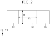
- FIG. 2 illustrates a top plan view of the thin film transistor according to an embodiment.
- a thin film transistor array substrate includes a substrate 110, a buffer layer 120, a semiconductor layer 130, a gate electrode 154, a first electrode 173, a second electrode 175, a first insulating layer 140, and a second insulating layer 160.
- the substrate 110 may include an insulating material.
- the buffer layer 120 may be an insulating layer and may be located on the substrate 110.
- the semiconductor layer 130 is positioned on the buffer layer 120.
- the semiconductor layer 130 includes a channel region 134 for forming a channel when the thin film transistor is turned on, conductive regions 133d and 135d positioned at opposite sides of the channel region 134, and edge portions 133 and 135.
- a first conductive region 133d positioned at one side may be a source region, and a second conductive region 135d positioned at the other side may be a drain region; or vice versa.
- the edge portions 133 and 135 have a higher concentration of doped carbon (C) compared with the remaining portions of the semiconductor layer 130, including the channel region 134 and the conductive regions 133d and 135d.
- C doped carbon
- carbon may not be substantially doped in the channel region 134 and the conductive regions 133d and 135d, but only the edge portions 133 and 135 may be substantially doped with carbon.
- a dose of carbon doped in the edge portions 133 and 135 may be in a range of about 1*10 11 /cm 2 to 1*10 13 /cm 2 .
- the conductive regions 133d and 135d and the edge portions 133 and 135 may all be conductive, and may have a higher carrier concentration than the channel region 134. Accordingly, the edge portions 133 and 135 may be considered as being included in the conductive regions 133d and 135d.
- the first edge portion 133 may be positioned at an edge of the first conductive region 133d, and the second edge portion 135 may be positioned at an edge of the second conductive region 135d.
- the first edge portion 133 may include a first vertical portion 133a extending in a direction perpendicular to a surface of the substrate 110, that is, in a z-direction, and contacting a side surface of the first conductive region 133d, and a first horizontal portion 133b extending in a y-direction perpendicular to the z-direction and contacting an upper surface of the first conductive region 133d.
- the first conductive region 133d may be positioned between the first vertical portion 133a and the channel region 134 and between the first horizontal portion 133b and the substrate 110.
- the first vertical portion 133a and the first horizontal portion 133b may be connected to each other a corner of the semiconductor layer 130.
- One side surface of the first horizontal portion 133b may directly contact one side surface of the channel region 134.
- the first vertical portion 133a and the first horizontal portion 133b connected to each other may substantially form a Hangul consonant ' ⁇ ' shape in a yz cross-sectional view.
- a y-directional length of the first horizontal portion 133b may be larger than a y-directional width of the first vertical portion 133a.
- a z-directional thickness of the first horizontal portion 133b may be smaller than a z-directional length of the first vertical portion 133a.
- a z-directional thickness of the first horizontal portion 133b may be in a range of about 1 angstrom to 50 angstroms.
- a y-directional width of the first vertical portion 133a may be in a range of about 1 angstrom to 100 angstroms.
- the second edge portion 135 may include a second vertical portion 135a extending in a direction perpendicular to a surface of the substrate 110, that is, in the z-direction, and contacting a side surface of the second conductive region 135d.
- the second edge portion 135 may include a second horizontal portion 135b extending in the y-direction and contacting an upper surface of the second conductive region 135d.
- the second vertical portion 135a and the second horizontal portion 135b may be connected to each other at a corner of the semiconductor layer 130.
- the second horizontal portion 135b and the first horizontal portion 133b may respectively contact two opposite side surfaces of the channel region 134.
- the second vertical portion 135a and the second horizontal portion 135b connected to each other may substantially form a Hangul consonant ' ⁇ ' shape in a yz cross-sectional view.
- a y-directional length of the second horizontal portion 135b may be larger than a y-directional width of the second vertical portion 135a.
- a z-directional thickness of the second horizontal portion 135b may be smaller than a z-directional length of the second vertical portion 135a.
- a z-directional thickness of the second horizontal portion 135b may be in a range of about 1 angstrom to 50 angstroms.
- a y-directional width of the second vertical portion 135a may be in a range of about 1 angstrom to 100 angstroms.
- the edge portions 133 and 135 may include two opposite side surfaces of the semiconductor layer 130, and may include two opposite end parts of an upper surface of the semiconductor layer 130 at two opposite sides of the channel region 134.
- the edge portions 133 and 135 may include outer edges of the semiconductor layer 130 positioned at opposite sides of the channel region 134 of the semiconductor layer 130.
- the semiconductor layer 130 may include a semiconductor material such as polycrystalline silicon, and the semiconductor layer 130 is entirely doped with an impurity other than carbon.
- the semiconductor layer 130 may be a P-type semiconductor or an N-type semiconductor.
- a dopant (that is, an impurity) doped into the semiconductor layer 130 may include a group 13 element such as boron (B), aluminium (Al), or indium (In).
- an impurity doped into the semiconductor layer 130 may include a group 15 element such as phosphorus (P), arsenic (As), or antimony (Sb).
- the semiconductor layer 130 may be doped with boron as a main impurity.
- the impurity doped in the semiconductor layer 130 means an impurity other than carbon.
- a dose of the impurity doped in the semiconductor layer 130 may be in a range of about 1*10 11 /cm 2 to 1*10 13 /cm 2 .
- a z-directional thickness of the semiconductor layer 130 may be in a range of about 400 angstroms to 500 angstroms.
- the first insulating layer 140 may be disposed on the semiconductor 130.
- the first insulating layer 140 is also referred to as a gate insulating layer.
- the gate electrode 154 may be positioned on the first insulating layer 140.
- the gate electrode 154 may overlap the channel region 134 of the semiconductor layer 130 in the z-direction.
- the gate electrode 154 may not overlap the conductive regions 133d and 135d in the z-direction.
- the gate electrode 154 may not overlap the edge portions 133 and 135 in the z-direction.
- the semiconductor layer 130 and the gate electrode 154 may form one thin film transistor.
- the thin film transistor array substrate includes a plurality of the thin film transistors.
- the second insulating layer 160 may be positioned on the gate electrode 154.
- At least one of the buffer layer 120, the first insulating layer 140, and the second insulating layer 160 may include an inorganic insulating material such as a silicon nitride (SiN x ), a silicon oxide (SiO x ), and/or a silicon oxynitride (SiO x N y ) and/or may include an organic insulating material such as a polyimide, an acryl-based polymer, and/or a siloxane-based polymer.
- an inorganic insulating material such as a silicon nitride (SiN x ), a silicon oxide (SiO x ), and/or a silicon oxynitride (SiO x N y ) and/or may include an organic insulating material such as a polyimide, an acryl-based polymer, and/or a siloxane-based polymer.
- a first electrode 173 and a second electrode 175 may be positioned on the second insulating layer 160.
- the first electrode 173 may contact an upper surface of the first horizontal portion 133b of the first edge portion 133 of the semiconductor layer 130 through an opening 163 formed in the second insulating layer 160 and the first insulating layer 140 to be electrically connected to the first edge portion 133.
- the second electrode 175 may contact an upper surface of the second horizontal portion 135b of the second edge portion 135 of the semiconductor layer 130 through an opening 165 formed in the second insulating layer 160 and the first insulating layer 140 to be electrically connected to the second edge portion 135.
- At least one of the gate electrode 154, the first electrode 173, and the second electrode 175 may include at least one of copper (Cu), aluminium (Al), magnesium (Mg), silver (Ag), gold (Au), platinum (Pt), palladium (Pd), nickel, (Ni), neodymium (Nd), iridium (Ir), molybdenum (Mo), tungsten (W), titanium (Ti), chromium (Cr), tantalum (Ta), and an alloy of some of the above metal materials.
- Each of the gate electrode 154, the first electrode 173, and the second electrode 175 may be formed as a single layer or a multilayer structure.
- edge portions 133 and 135 additionally doped with carbon are positioned at sides and upper surface portions of the semiconductor layer 130 like walls, impurities such as boron doped in the semiconductor layer 130 are prevented from diffusing into elements outside the semiconductor layer 130 such as other thin film transistors.
- the carbon doped in the edge portions 133 and 135 may affect residual dangling bonds in the semiconductor layer 130 to prevent impurity diffusion. Accordingly, embodiments may minimize deviation of characteristics such as on/off ratios, threshold voltages, and leakage currents of the plurality of thin film transistors.
- each of the channel length Wa and a channel width Wb of the short channel thin film transistor may be in a range of about 1.5 micrometers to 2.0 micrometers.
- the impurities such as boron
- the impurities may diffuse beyond the semiconductor layer 130, so that there may be deviation of the characteristics of the thin film transistor.
- embodiments may maintain substantially consistent characteristics of the thin film transistor.
- high-speed driving and variable frequency driving of electronic devices may be effectively realized, and characteristics of high-resolution display devices in which thin film transistors are disposed with high density may be satisfactory.
- a method for manufacturing a thin film transistor array substrate according to one or more embodiments are described with reference to FIG. 3 to FIG. 6 together with the previously described FIG. 1 and FIG. 2 .
- FIG. 3 illustrates a cross-sectional view of a structure corresponding to a process step of the method according to an embodiment.
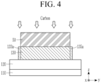
- FIG. 4 illustrates a cross-sectional view of a structure corresponding to a step after the step shown in FIG. 3 according to an embodiment.
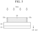
- FIG. 5 illustrates a cross-sectional view of a structure corresponding to a step after the step shown in FIG. 4 according to an embodiment.
- FIG. 6 illustrates a cross-sectional view of a structure (e.g., a thin film transistor array substrate) corresponding to a step after the step shown in FIG. 5 according to an embodiment.
- a structure e.g., a thin film transistor array substrate
- an insulating material such as a silicon nitride (SiN x ) and/or a silicon oxide (SiO x ), is provided on the substrate 110 to form the buffer layer 120.
- a semiconductor material layer is provided on the buffer layer 120, a mask pattern 50 is formed on the semiconductor material layer to partially cover the semiconductor material layer, and then the semiconductor material layer is etched or patterned using the mask pattern 50 as a mask to form the semiconductor layer 130.
- amorphous silicon (a-Si) is first deposited on the buffer layer 120 to form an amorphous silicon layer, and the amorphous silicon layer is crystallized to form the polycrystalline silicon semiconductor layer 130.
- a crystallization method may include an annealing process using a heat source such as excimer laser.
- the mask pattern 50 may include a photoresist.
- side portions of the mask pattern 50 may be removed.
- an ashing process using oxygen gas (O 2 ) may be performed.
- an upper portion of the mask pattern 50 may also be removed, so that a thickness of the mask pattern 50 in the z-direction may be reduced.
- a dimension of the mask pattern 50 in each of the x-direction, y-direction, and z-direction may be reduced by etching the mask pattern 50.
- edge portions of the semiconductor layer 130 are not covered by the mask pattern 50 and are exposed.
- a set of carbon is primarily injected from above the mask pattern 50. Consequently, the edge portions of the semiconductor layer 130 exposed by the mask pattern 50 may be doped with carbon to form the first vertical portion 133a and the second vertical portion 135a. In a portion of the semiconductor layer 130 covered by the mask pattern 50, because the mask pattern 50 blocks carbon, carbon may hardly be doped.
- a carbon acceleration voltage may be in a range of about 10 keV to 40 keV.
- the mask pattern 50 is removed, and impurities such as boron are doped on the entire exposed semiconductor layer 130. Accordingly, the entire semiconductor layer 130 including the first vertical portion 133a and the second vertical portion 135a is doped with impurities such as boron.
- An acceleration voltage of boron during the doping may be in a range of about 1 keV to 10 keV.
- the first insulating layer 140 is formed by providing an insulating material on the semiconductor layer 130, and a conductive material such as a metal is provided on the first insulating layer 140 and patterned to form the gate electrode 154.
- the gate electrode 154 overlaps a region designated to be a channel region in the semiconductor layer 130 and does not overlap edge portions of the semiconductor layer 130.
- an impurity such as boron is injected from above the gate electrode 154 to form the conductive regions 133d and 135d at opposite sides of the channel region 134.
- a set of carbon is secondarily injected from above the gate electrode 154.
- the region of the semiconductor layer 130 covered by the gate electrode 154 is blocked from being doped with carbon, and carbon may be doped on the upper edge portions of the semiconductor layer 130 not covered by the gate electrode 154 in the z-direction to form the first horizontal portion 133b and the second horizontal portion 135b.
- a secondary carbon doping depth may be smaller than a primary carbon doping depth. Therefore, z-directional thicknesses of the first horizontal portion 133b and the second horizontal portion 135b are smaller than z-directional lengths of the first vertical portion 133a and the second vertical portion 135a. For this purpose, a secondary carbon doping concentration or time may be smaller than a primary carbon doping concentration or time.
- Upper edge portions of the semiconductor layer 130 may be formed as the first horizontal portion 133b and the second horizontal portion 135b depending on a dose of the secondary carbon.
- Lower edge portions of the first insulating layer 140 contacting the upper surfaces of the first horizontal portion 133b and the second horizontal portion 135b may also be doped with carbon to form a first additional horizontal portion 133c and a second additional horizontal portion 135c shown in FIG. 6 .
- the first additional horizontal portion 133c may be in contact with the first horizontal portion 133b and may be continuously formed with the first horizontal portion 133b in the z-direction
- the second additional horizontal portion 135c may be in contact with the second horizontal portion 135b and may be continuously formed with the second horizontal portion 135b in the z-direction.
- the first additional horizontal portion 133c and the second additional horizontal portion 135c may not overlap the gate electrode 154 in the z-direction.
- the first additional horizontal portion 133c and the second additional horizontal portion 135c are included in the first insulating layer 140 and may be insulative.
- first additional horizontal portion 133c and the second additional horizontal portion 135c may not be formed by adjusting the dose of the secondary carbon.
- only edge portions 133 and 135 may be formed in the carbon-doped semiconductor layer 130, as shown in FIG. 1 described above.
- the second insulating layer 160 is formed by depositing an insulating material on the gate electrode 154. Subsequently, openings 163 and 165 are formed by patterning the first insulating layer 140 and the second insulating layer 160. Subsequently, a conductive material such as a metal is provided on the second insulating layer 160 and patterned to form the first electrode 173 and the second electrode 175.
- a method for manufacturing a thin film transistor array substrate according to one or more embodiments are described with reference to FIG. 7 to FIG. 9 together with some of the previously described drawings, particularly, FIG. 3 to FIG. 5 .
- FIG. 7 illustrates a cross-sectional view of a structure corresponding to a step after the step shown in FIG. 5 according to an embodiment.
- FIG. 8 illustrates a cross-sectional view of a structure corresponding to a step after the step shown in FIG. 7 according to an embodiment.
- FIG. 9 illustrates a cross-sectional view of a structure corresponding to a step after the step shown in FIG. 8 according to an embodiment.
- the method may include features that are identical to and/or similar to features described with reference to FIG. 3 to FIG. 6 , but the process steps after the process step shown in FIG. 5 may be different.
- a passivation layer 180 is formed by providing an insulating material such as a silicon nitride (SiN x ), a silicon oxide (SiO x ), or a silicon oxynitride (SiO x N y ) on the semiconductor layer 130.
- a mask pattern 60 is formed on the passivation layer 180.
- the mask pattern 60 overlaps a region designated to be a channel region in the semiconductor layer 130 and does not overlap edge portions of the semiconductor layer 130.
- the mask pattern 60 may include inorganic material and/or an organic material, such as a metal and/or a photoresist.
- an impurity such as boron is injected from above the mask pattern 60 to form the conductive regions 133d and 135d at opposite sides of the channel region 134.
- a set of carbon is secondarily doped from above the mask pattern 60 (wherein primary carbon doping is the same as the step described with reference to FIG. 4 ).
- This secondary carbon doping may be performed under the same condition as the secondary carbon doping described above.
- the region of the semiconductor layer 130 overlapping the mask pattern 60 is blocked from being doped with carbon, and carbon may be doped on the upper edge portions of the semiconductor layer 130 not overlapped by the mask pattern 60 in the z-direction to form the first horizontal portion 133b and the second horizontal portion 135b.
- a secondary carbon doping depth may be controlled. During the secondary carbon doping, damage to the upper portion of the semiconductor layer 130 may be reduced by the passivation layer 180.
- Upper edge portions of the semiconductor layer 130 may be formed as the first horizontal portion 133b and the second horizontal portion 135b depending on a dose of the secondary carbon.
- Lower edge portions of the passivation layer 180 contacting the upper surfaces of the first horizontal portion 133b and the second horizontal portion 135b may also be doped with carbon to form a first additional horizontal portion 133c and a second additional horizontal portion 135c shown in FIG. 7 .
- the first additional horizontal portion 133c may be in contact with the first horizontal portion 133b and may be continuously formed with the first horizontal portion 133b in the z-direction
- the second additional horizontal portion 135c may be in contact with the second horizontal portion 135b and may be continuously formed with the second horizontal portion 135b in the z-direction.
- the first additional horizontal portion 133c and the second additional horizontal portion 135c may not overlap the mask pattern 60 in the z-direction.
- the mask pattern 60 and the passivation layer 180 are removed using an etching process or the like.
- the first additional horizontal portion 133c and the second additional horizontal portion 135c may also be removed. Accordingly, the edge portions 133 and 135 illustrated in FIG. 1 described above may be formed.
- the first insulating layer 140 is formed by providing an insulating material on the semiconductor layer 130, and a conductive material such as a metal is provided on the first insulating layer 140 and patterned to form the gate electrode 154.
- the second insulating layer 160 is formed by providing an insulating material on the gate electrode 154.
- the openings 163 and 165 are formed by patterning the first insulating layer 140 and the second insulating layer 160.
- a conductive material such as a metal is provided on the second insulating layer 160 and patterned to form the first electrode 173 and the second electrode 175.
- One or more methods for manufacturing a thin film transistor array substrate according to one or more embodiments are described with reference to FIG. 10 to FIG. 15 together with the previously described FIG. 3 and FIG. 6 .
- FIG. 10 illustrates a cross-sectional view of a structure corresponding to a process step of the method according to an embodiment.
- FIG. 11 illustrates a cross-sectional view of a structure corresponding to a step after the step shown in FIG. 10 according to an embodiment.
- FIG. 12 illustrates a cross-sectional view of a structure corresponding to a step after the step shown in FIG. 11 according to an embodiment.
- FIG. 13 illustrates a cross-sectional view of a structure corresponding to a step after the step shown in FIG. 12 according to an embodiment.
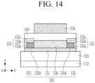
- FIG. 14 illustrates a cross-sectional view of a structure corresponding to a step after the step shown in FIG. 13 according to an embodiment.
- FIG. 15 illustrates a cross-sectional view of a structure corresponding to a step after the step shown in FIG. 13 according to an embodiment.
- an insulating material such as a silicon nitride (SiN x ) and/or a silicon oxide (SiO x ) is provided on the substrate 110 to form the buffer layer 120.
- carbon is injected from below the substrate 110 and through the substrate 110 to primarily dope carbon into at least a portion of a lower portion of the semiconductor layer 130a to form a doped layer 131a at the lower portion of the semiconductor layer 130a.
- Only the lower portion of the semiconductor layer 130a may be the doped layer 131a, or unlike the structure shown in FIG. 11 , the entire semiconductor layer 130a may be doped with carbon to form the doped layer 131a.
- an additional semiconductor layer 130b is formed by further providing a semiconductor material such as a material of the semiconductor layer 130a on the semiconductor layer 130a. There may be no substantial boundary between the semiconductor layer 130a and the additional semiconductor layer 130b, and the semiconductor layer 130a and the additional semiconductor layer 130b together may form a substantially single semiconductor layer (i.e., a combined semiconductor layer).
- a crystallization method may include an annealing process using a heat source such as an excimer laser.
- the semiconductor layer 130a, the additional semiconductor layer 130b, and the doped layer 131a are etched to form the semiconductor layer 130 including the patterned semiconductor layer 130a, the additional semiconductor layer 130b, and the bottom portion 131 as shown in FIG. 13 .
- Subsequent process steps may be the same as or similar to process steps described with reference to some of FIG. 4 to FIG. 6 and/or some of FIGS. 7 to FIG. 9 .
- the subsequent process steps may include at least two carbon doping steps for the side portions and upper edge portions of the semiconductor layer 130.
- FIG. 14 and FIG. 15 may illustrate a structure of a thin film transistor and/or a thin film transistor array substrate.
- the structure of the thin film transistor included in the thin film transistor array substrate shown in FIG. 14 is substantially the same as the structure of the thin film transistor shown in FIG. 6 , but the semiconductor layer 130 further includes the bottom portion 131 doped with carbon and positioned at an interface with the buffer layer 120.
- the bottom portion 131 may be referred to as an intermediate region.
- a concentration of carbon doped in the bottom portion 131 is higher than those of the channel region 134 and the conductive regions 133d and 135d of the semiconductor layer 130.
- carbon may not be substantially doped in the channel region 134 and the conductive regions 133d and 135d, but only the edge portions 133 and 135 and the bottom portion 131 may be substantially doped with carbon.
- the bottom portion 131 may be formed from a lowermost surface of the semiconductor layer 130 up to a predetermined thickness, and may be in contact with the entire lower surfaces of the channel region 134, the first vertical portion 133a, and the second vertical portion 135a.
- the bottom portion 131 may include the entire bottom surface of the semiconductor layer 130 to which it belongs.
- the structure of the thin film transistor included in the thin film transistor array substrate shown in FIG. 15 is substantially the same as the structure of the thin film transistor shown in FIG. 1 or FIG. 9 , but the semiconductor layer 130 illustrated in FIG. 15 includes the bottom portion 131 doped with carbon and positioned at an interface with the buffer layer 120.
- the characteristics of the bottom part 131 shown in FIG. 15 may be the same as those of the bottom portion 131 shown in FIG. 14 .
- the bottom portion 131 doped with carbon and the edge portions 133 and 135 together form a container that substantially surrounds/encloses the channel region 134, the conductive region 133d, and the conductive region 135d except for the upper surface of the channel region 134.
- the container may effectively block an impurity such as boron of the semiconductor layer 130 from being undesirably diffused beyond the semiconductor layer 130 to other thin film transistors.
- a thin film transistor, a thin film transistor array substrate, and a related manufacturing method according to one or more embodiments are described with reference to FIG. 16 and FIG. 17 together with the previously described FIG. 1 to FIG. 6 .
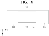
- FIG. 16 illustrates a top plan view of a thin film transistor according to an embodiment.
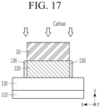
- FIG. 17 illustrates a cross-sectional view of a structure corresponding to a process step of the method to an embodiment.
- the thin film transistor may be the same as the thin film transistor shown in FIG. 1 and FIG. 2 , but the semiconductor layer shown in FIG. 16 may further include side portions 136 positioned at opposite sides of the channel region 134 that are opposite in the x-direction.
- the side portions 136 may be positioned between the first and second conductive regions 133d and 135d in the y-direction.
- Each of the side portions 136 may extend lengthwise in the y-direction.
- the side portions 136 may have a higher concentration of doped carbon compared with the channel region 134, for blocking boron potentially diffused from the channel region 134.
- the concentration of carbon doped in the side portions 136 may be lower than the concentration of carbon doped in the edge portions 133 and 135.
- a carrier concentration of the side portion 136 may be lower than a carrier concentration of the conductive regions 133d and 135d.
- the gate electrode 154 may be positioned on the side portions 136 and may overlap the side portions 136 in the z-direction.
- the method for manufacturing the thin film transistor array substrate including the thin film transistor shown in FIG. 16 is substantially the same as the method described with reference to FIG. 3 to FIG. 6 , but in the process step shown in FIG. 4 , when a portion of the side portion of the mask pattern 50 is removed, four sides of the semiconductor layer 130 may be exposed without being covered by the mask pattern 50. Not only two opposite sides of the semiconductor layer 130 opposite each other in the y-direction (shown in FIG. 4 ) but also two opposite sides of the semiconductor layer 130 opposite each other in the x-direction shown in FIG. 17 may be exposed without being covered by the mask pattern 50.
- the four exposed sides of the semiconductor layer 130 may form a closed shape such as a quadrangle.
- first vertical portion 133a and the second vertical portion 135a shown in FIG. 4
- side portions 136 shown in FIG. 17 may also be formed.
- the first vertical portion 133a, the second vertical portion 135, and the side portions 136 may be connected to each other to form a single closed figure in a plan view of the semiconductor layer 130.
- Subsequent process steps may be the same as some process steps described with reference to FIG. 5 and FIG. 6 .
- first horizontal portion 133b and the second horizontal portion 135b described above may be optional.
- the secondary carbon doping process for forming the first horizontal portion 133b and the second horizontal portion 135b may be optional.
- FIG. 18 illustrates a schematic top plan view of a display device according to an embodiment.
- the display device may include a display area DA (including a plurality of pixels PX) and a peripheral area PA around the display area DA.
- a driving circuit DR for driving the pixels PX may be positioned in the peripheral area PA.
- the display device may include a thin film transistor array substrate described with reference to one or more of FIG. 1 to FIG. 17 .
- Each pixel PX and/or the driving circuit DR may include a thin film transistor described with reference to one or more of FIG. 1 to FIG. 17 .
- Embodiments may prevent doped impurities (e.g., boron) in the semiconductor layer from diffusing into other layers or other thin film transistors. Therefore, characteristics of thin film transistors in the display device may be sufficiently consistent and/or sufficiently uniform.
- the performance of the display device may be satisfactory.
- the present invention relates to a thin film transistor array substrate and a method of manufacturing the same.
Landscapes
- Thin Film Transistor (AREA)
- Chemical & Material Sciences (AREA)
- Crystallography & Structural Chemistry (AREA)
Abstract
Description
- The present disclosure relates to a thin film transistor array substrate and a method for manufacturing the thin film transistor array.
- A semiconductor device, such as a display device, may include a thin film transistor array substrate on which a plurality of thin film transistors for performing switching functions or for controlling electronic elements are formed. For example, a display device may include thin film transistors positioned in a display area capable of displaying an image and may include thin film transistors positioned in a circuit of a peripheral area.
- A thin film transistor includes a semiconductor layer, which is an active layer formed on a substrate, and a gate electrode. A gate insulating layer is positioned between the semiconductor layer and the gate electrode.
- The semiconductor layer may include various semiconductor materials such as amorphous silicon, polycrystalline silicon, or oxide semiconductor, and the semiconductor layer may be doped with an impurity for electrical properties
Among the plurality of transistors included in a semiconductor device, the smaller the distribution of transistors for the same function, the more uniform the characteristics can be. - The present embodiments provide a thin film transistor array substrate including thin film transistors that may prevent unnecessary diffusion of a dopant or impurity and a manufacturing method thereof such that unwanted deviation of characteristics of the thin film transistors may be minimized, and the performance of the thin film transistors may be sufficiently consistent and uniform.
- A thin film transistor array substrate accordingly to an embodiment includes a substrate; a semiconductor layer on the substrate; and a gate electrode on the semiconductor layer, wherein the semiconductor layer includes a channel region, conductive regions positioned on both sides of the channel region, and an edge portion; the edge portion is positioned at an edge of the conductive region; and the edge portion is doped with high concentration of carbon compared with the channel region and the conductive region.
- The edge portion may include a vertical portion that extends in a first direction perpendicular to a surface of the substrate and contacts a side surface of the conductive region.
- The edge portion may further include a horizontal portion that extends in a second direction different from the first direction and contacts an upper surface of the conductive region.
- The vertical portion and the horizontal portion may be connected to each other at corners thereof.
- One side surface of the horizontal portion may be in contact with one side surface of the channel region.
- A width of the horizontal portion in the first direction may be smaller than a length of the vertical portion in the first direction, and a length of the horizontal portion in the second direction may be larger than a width of the vertical portion in the second direction.
- The thin film transistor array substrate may further include: an insulating layer positioned on the gate electrode; and an electrode positioned on the insulating layer, wherein the electrode may contact an upper surface of the horizontal portion of the edge portion through an opening formed in the insulating layer to be electrically connected thereto.
- The thin film transistor array substrate may further include an insulating layer positioned between the semiconductor layer and the gate electrode, wherein a lower portion of the insulating layer may be doped with carbon and may include an additional horizontal portion contacting the horizontal portion.
- The semiconductor layer may further include a bottom portion that is positioned thereunder and is doped with carbon having a higher concentration than that of the channel region and the conductive region.
- The edge portion and the bottom portion together may surround bottom and side surfaces of the semiconductor layer, and an entire upper surface of the semiconductor layer excluding an upper surface of the channel region.
- The edge portion may be conductive.
- The semiconductor layer may include polycrystalline silicon.
- A method for manufacturing a thin film transistor array substrate accordingly to an embodiment includes forming a semiconductor layer on a substrate; forming a first mask pattern on the semiconductor layer to expose an edge portion of the semiconductor layer; primarily doping carbon in the semiconductor layer by using the first mask pattern as a mask; removing the first mask pattern, and doping an impurity in the exposed semiconductor layer; and forming a first insulating layer on the semiconductor layer.
- The manufacturing method of the thin film transistor array substrate may further include forming a second mask pattern on the first insulating layer; and secondarily doping carbon in the semiconductor layer by using the second mask pattern as a mask.
- The manufacturing method of the thin film transistor array substrate may further include: removing the first insulating layer; forming a second insulating layer on the semiconductor layer; and forming a gate electrode on the second insulating layer.
- The manufacturing method of the thin film transistor array substrate may further include: forming a gate electrode on the first insulating layer; and secondarily doping carbon in the semiconductor layer by using the gate electrode as a mask.
- The manufacturing method of the thin film transistor array substrate may further include: forming a second insulating layer on the gate electrode; forming an opening in the second insulating layer and the first insulating layer; and forming an electrode connected to the semiconductor layer through the opening.
- The manufacturing method of the thin film transistor array substrate may further include forming a bottom portion doped with carbon in a lower portion of the semiconductor layer by injecting carbon into the lower portion of the semiconductor layer.
- A method for manufacturing a thin film transistor array substrate accordingly to an embodiment includes stacking amorphous silicon on a substrate to form a first semiconductor layer; forming a lower doped layer by primarily doping carbon in a lower portion of the first semiconductor layer by injecting carbon from a lower part of the substrate; stacking amorphous silicon on the first semiconductor layer to form an additional semiconductor layer; forming a first mask pattern exposing an edge portion of a second semiconductor layer on the second semiconductor layer including the lower doped layer, the first semiconductor layer, and the additional semiconductor layer; primarily doping carbon in the second semiconductor layer by using the first mask pattern as a mask; removing the first mask pattern, and doping an impurity in the exposed second semiconductor layer; and forming a first insulating layer on the second semiconductor layer.
- The manufacturing method of the thin film transistor array substrate may further include: forming a second mask pattern on the first insulating layer; and secondarily doping carbon in the semiconductor layer by using the second mask pattern as a mask.
- A thin film transistor array substrate according to an embodiment includes a channel region; a first region doped with a first material; and a second region doped with a second material, wherein the first region is in contact with the channel region to be positioned at both ends of the channel region, and the second region overlaps the first region and is in contact with the channel region.
- The first material may include boron.
- The second material may include carbon.
- According to the embodiments of the present invention, diffusion of a dopant or impurity in a thin film transistor or a thin film transistor array, such that unwanted deviation of characteristics of the thin film transistors may be minimized, and the performance of the thin film transistors may be sufficiently consistent and uniform.
-
-
FIG. 1 illustrates a cross-sectional view of a thin film transistor array substrate according to an embodiment. -
FIG. 2 illustrates a top plan view of a thin film transistor according to an embodiment. -
FIG. 3 illustrates a cross-sectional view of a structure corresponding to a process step in a method for manufacturing a thin film transistor array substrate according to an embodiment. -
FIG. 4 illustrates a cross-sectional view of a structure corresponding to a step after the step shown inFIG. 3 according to an embodiment. -
FIG. 5 illustrates a cross-sectional view of a structure corresponding to a step after the step shown inFIG. 4 according to an embodiment. -
FIG. 6 illustrates a cross-sectional view of a structure corresponding to a step after the step shown inFIG. 5 according to an embodiment. -
FIG. 7 illustrates a cross-sectional view of a structure corresponding to a step after the step shown inFIG. 5 according to an embodiment. -
FIG. 8 illustrates a cross-sectional view of a structure corresponding to a step after the step shown inFIG. 7 according to an embodiment. -
FIG. 9 illustrates a cross-sectional view of a structure corresponding to a step after the step shown inFIG. 8 according to an embodiment. -
FIG. 10 illustrates a cross-sectional view of a structure corresponding to a process step of a method for manufacturing a thin film transistor array substrate according to an embodiment. -
FIG. 11 illustrates a cross-sectional view of a structure corresponding to a step after the step shown inFIG. 10 according to an embodiment. -
FIG. 12 illustrates a cross-sectional view of a structure corresponding to a step after the step shown inFIG. 11 according to an embodiment. -
FIG. 13 illustrates a cross-sectional view of a structure corresponding to a step after the step shown inFIG. 12 according to an embodiment. -
FIG. 14 illustrates a cross-sectional view of a structure corresponding to a step after the step shown inFIG. 13 according to an embodiment. -
FIG. 15 illustrates a cross-sectional view of a structure corresponding to a step after the step shown inFIG. 13 according to an embodiment. -
FIG. 16 illustrates a top plan view of a thin film transistor according to an embodiment. -
FIG. 17 illustrates a cross-sectional view of a structure corresponding to a process step of a method for manufacturing a thin film transistor array substrate according to an embodiment. -
FIG. 18 illustrates a schematic top plan view of a display device according to an embodiment. - A thin film transistor array substrate accordingly to an embodiment includes a substrate; a semiconductor layer on the substrate; and a gate electrode on the semiconductor layer, wherein the semiconductor layer includes a channel region, conductive regions positioned on both sides of the channel region, and an edge portion; the edge portion is positioned at an edge of the conductive region; and the edge portion is doped with high concentration of carbon compared with the channel region and the conductive region.
- A method for manufacturing a thin film transistor array substrate accordingly to an embodiment includes forming a semiconductor layer on a substrate; forming a first mask pattern on the semiconductor layer to expose an edge portion of the semiconductor layer; primarily doping carbon in the semiconductor layer by using the first mask pattern as a mask; removing the first mask pattern, and doping an impurity in the exposed semiconductor layer; and forming a first insulating layer on the semiconductor layer.
- A method for manufacturing a thin film transistor array substrate accordingly to an embodiment includes stacking amorphous silicon on a substrate to form a first semiconductor layer; forming a lower doped layer by primarily doping carbon in a lower portion of the first semiconductor layer by injecting carbon from a lower part of the substrate; stacking amorphous silicon on the first semiconductor layer to form an additional semiconductor layer; forming a first mask pattern exposing an edge portion of a second semiconductor layer on the second semiconductor layer including the lower doped layer, the first semiconductor layer, and the additional semiconductor layer; primarily doping carbon in the second semiconductor layer by using the first mask pattern as a mask; removing the first mask pattern, and doping an impurity in the exposed second semiconductor layer; and forming a first insulating layer on the second semiconductor layer.
- A thin film transistor array substrate according to an embodiment includes a channel region; a first region doped with a first material; and a second region doped with a second material, wherein the first region is in contact with the channel region to be positioned at both ends of the channel region, and the second region overlaps the first region and is in contact with the channel region.
- Hereinafter, with reference to attached drawings, various embodiments of the present invention will be described in detail so that those skilled in the art can easily implement the present invention. The invention may be implemented in many different forms and is not limited to the embodiments described herein.
- In order to clearly explain the present invention, parts that are not relevant to the description are omitted, and identical or similar components are assigned with the same reference numerals throughout the specification.
- In addition, the size and thickness of each component shown in the drawings are shown arbitrarily for convenience of explanation, so the present invention is not necessarily limited to what is shown. In the drawing, the thickness is enlarged to clearly express various layers and areas. In the drawings, for convenience of explanation, the thicknesses of some layers and regions are exaggerated.
- Additionally, when a part of a layer, membrane, region, plate, etc. is said to be "on" or "above" another part, this includes not only cases where it is "directly on" another part, but also cases where there is another part in therebetween. Conversely, when a part is said to be "directly on" another part, it means that there is no other part therebetween. In addition, being "on" or "above" a reference part means being located above or below the reference part, and does not necessarily mean being located "above" or "on" in the direction opposite to gravity direction.
- In addition, throughout the specification, when a part is said to "include" a certain component, this means that it may further include other components rather than excluding other components, unless specifically stated to the contrary.
- In addition, throughout the specification, when referring to "in a plan view," this means when the target portion is viewed from above, and when referring to "in a cross-sectional view," this means when a cross section of the target portion is cut vertically and viewed from the side.
- A thin film transistor and a thin film transistor array substrate according to an embodiment will be described with reference to
FIGS. 1 and2 . -
FIG. 1 illustrates a cross-sectional view of a thin film transistor array substrate according to an embodiment.FIG. 2 illustrates a top plan view of the thin film transistor according to an embodiment. - Referring to
FIG. 1 , a thin film transistor array substrate according to an embodiment, also referred to as a transistor substrate, includes asubstrate 110, abuffer layer 120, asemiconductor layer 130, agate electrode 154, afirst electrode 173, asecond electrode 175, a first insulatinglayer 140, and a second insulatinglayer 160. Thesubstrate 110 may include an insulating material. Thebuffer layer 120 may be an insulating layer and may be located on thesubstrate 110. - The
semiconductor layer 130 is positioned on thebuffer layer 120. - The
semiconductor layer 130 includes achannel region 134 for forming a channel when the thin film transistor is turned on,conductive regions channel region 134, andedge portions - With respect to the
channel region 134, a firstconductive region 133d positioned at one side may be a source region, and a secondconductive region 135d positioned at the other side may be a drain region; or vice versa. - The
edge portions semiconductor layer 130, including thechannel region 134 and theconductive regions semiconductor layer 130, carbon may not be substantially doped in thechannel region 134 and theconductive regions edge portions - A dose of carbon doped in the
edge portions - The
conductive regions edge portions channel region 134. Accordingly, theedge portions conductive regions - The
first edge portion 133 may be positioned at an edge of the firstconductive region 133d, and thesecond edge portion 135 may be positioned at an edge of the secondconductive region 135d. - The
first edge portion 133 may include a firstvertical portion 133a extending in a direction perpendicular to a surface of thesubstrate 110, that is, in a z-direction, and contacting a side surface of the firstconductive region 133d, and a firsthorizontal portion 133b extending in a y-direction perpendicular to the z-direction and contacting an upper surface of the firstconductive region 133d. The firstconductive region 133d may be positioned between the firstvertical portion 133a and thechannel region 134 and between the firsthorizontal portion 133b and thesubstrate 110. - The first
vertical portion 133a and the firsthorizontal portion 133b may be connected to each other a corner of thesemiconductor layer 130. One side surface of the firsthorizontal portion 133b may directly contact one side surface of thechannel region 134. - The first
vertical portion 133a and the firsthorizontal portion 133b connected to each other may substantially form a Hangul consonant '¬' shape in a yz cross-sectional view. - A y-directional length of the first
horizontal portion 133b may be larger than a y-directional width of the firstvertical portion 133a. A z-directional thickness of the firsthorizontal portion 133b may be smaller than a z-directional length of the firstvertical portion 133a. For example, a z-directional thickness of the firsthorizontal portion 133b may be in a range of about 1 angstrom to 50 angstroms. A y-directional width of the firstvertical portion 133a may be in a range of about 1 angstrom to 100 angstroms. - The
second edge portion 135 may include a secondvertical portion 135a extending in a direction perpendicular to a surface of thesubstrate 110, that is, in the z-direction, and contacting a side surface of the secondconductive region 135d. Thesecond edge portion 135 may include a secondhorizontal portion 135b extending in the y-direction and contacting an upper surface of the secondconductive region 135d. - The second
vertical portion 135a and the secondhorizontal portion 135b may be connected to each other at a corner of thesemiconductor layer 130. The secondhorizontal portion 135b and the firsthorizontal portion 133b may respectively contact two opposite side surfaces of thechannel region 134. - The second
vertical portion 135a and the secondhorizontal portion 135b connected to each other may substantially form a Hangul consonant '¬' shape in a yz cross-sectional view. - A y-directional length of the second
horizontal portion 135b may be larger than a y-directional width of the secondvertical portion 135a. A z-directional thickness of the secondhorizontal portion 135b may be smaller than a z-directional length of the secondvertical portion 135a. For example, a z-directional thickness of the secondhorizontal portion 135b may be in a range of about 1 angstrom to 50 angstroms. A y-directional width of the secondvertical portion 135a may be in a range of about 1 angstrom to 100 angstroms. - Referring to
FIG. 1 andFIG. 2 , theedge portions semiconductor layer 130, and may include two opposite end parts of an upper surface of thesemiconductor layer 130 at two opposite sides of thechannel region 134. Theedge portions semiconductor layer 130 positioned at opposite sides of thechannel region 134 of thesemiconductor layer 130. - The
semiconductor layer 130 may include a semiconductor material such as polycrystalline silicon, and thesemiconductor layer 130 is entirely doped with an impurity other than carbon. - The
semiconductor layer 130 may be a P-type semiconductor or an N-type semiconductor. - When the
semiconductor layer 130 is a P-type semiconductor, a dopant (that is, an impurity) doped into thesemiconductor layer 130 may include a group 13 element such as boron (B), aluminium (Al), or indium (In). When thesemiconductor layer 130 is an N-type semiconductor, an impurity doped into thesemiconductor layer 130 may include a group 15 element such as phosphorus (P), arsenic (As), or antimony (Sb). Thesemiconductor layer 130 may be doped with boron as a main impurity. In the description, the impurity doped in thesemiconductor layer 130 means an impurity other than carbon. - A dose of the impurity doped in the
semiconductor layer 130 may be in a range of about 1*1011/cm2 to 1*1013/cm2. - A z-directional thickness of the
semiconductor layer 130 may be in a range of about 400 angstroms to 500 angstroms. - The first insulating
layer 140 may be disposed on thesemiconductor 130. The first insulatinglayer 140 is also referred to as a gate insulating layer. - The
gate electrode 154 may be positioned on the first insulatinglayer 140. Thegate electrode 154 may overlap thechannel region 134 of thesemiconductor layer 130 in the z-direction. - The
gate electrode 154 may not overlap theconductive regions gate electrode 154 may not overlap theedge portions - The
semiconductor layer 130 and thegate electrode 154 may form one thin film transistor. The thin film transistor array substrate includes a plurality of the thin film transistors. - The second
insulating layer 160 may be positioned on thegate electrode 154. - At least one of the
buffer layer 120, the first insulatinglayer 140, and the second insulatinglayer 160 may include an inorganic insulating material such as a silicon nitride (SiNx), a silicon oxide (SiOx), and/or a silicon oxynitride (SiOxNy) and/or may include an organic insulating material such as a polyimide, an acryl-based polymer, and/or a siloxane-based polymer. - A
first electrode 173 and asecond electrode 175 may be positioned on the second insulatinglayer 160. - The
first electrode 173 may contact an upper surface of the firsthorizontal portion 133b of thefirst edge portion 133 of thesemiconductor layer 130 through anopening 163 formed in the second insulatinglayer 160 and the first insulatinglayer 140 to be electrically connected to thefirst edge portion 133. - The
second electrode 175 may contact an upper surface of the secondhorizontal portion 135b of thesecond edge portion 135 of thesemiconductor layer 130 through anopening 165 formed in the second insulatinglayer 160 and the first insulatinglayer 140 to be electrically connected to thesecond edge portion 135. - At least one of the
gate electrode 154, thefirst electrode 173, and thesecond electrode 175 may include at least one of copper (Cu), aluminium (Al), magnesium (Mg), silver (Ag), gold (Au), platinum (Pt), palladium (Pd), nickel, (Ni), neodymium (Nd), iridium (Ir), molybdenum (Mo), tungsten (W), titanium (Ti), chromium (Cr), tantalum (Ta), and an alloy of some of the above metal materials. Each of thegate electrode 154, thefirst electrode 173, and thesecond electrode 175 may be formed as a single layer or a multilayer structure. - In the
semiconductor layer 130 of the thin film transistor, since theedge portions semiconductor layer 130 like walls, impurities such as boron doped in thesemiconductor layer 130 are prevented from diffusing into elements outside thesemiconductor layer 130 such as other thin film transistors. The carbon doped in theedge portions semiconductor layer 130 to prevent impurity diffusion. Accordingly, embodiments may minimize deviation of characteristics such as on/off ratios, threshold voltages, and leakage currents of the plurality of thin film transistors. - Referring to
FIG. 2 , when an electronic device, e.g., a display device, including the thin film transistor array substrate has high resolution, requires high-speed driving, and/or requires variable frequency driving, a short channel thin film transistor having a shorter channel length Wa of the thin film transistor is required. For example, each of the channel length Wa and a channel width Wb of the short channel thin film transistor may be in a range of about 1.5 micrometers to 2.0 micrometers. - As the channel length Wa of the thin film transistor becomes shorter, if not properly blocked, the impurities (such as boron) doped in the
semiconductor layer 130 may diffuse beyond thesemiconductor layer 130, so that there may be deviation of the characteristics of the thin film transistor. By blocking the impurities from diffusing beyond thesemiconductor layer 130, embodiments may maintain substantially consistent characteristics of the thin film transistor. Advantageously, high-speed driving and variable frequency driving of electronic devices may be effectively realized, and characteristics of high-resolution display devices in which thin film transistors are disposed with high density may be satisfactory. - A method for manufacturing a thin film transistor array substrate according to one or more embodiments are described with reference to
FIG. 3 to FIG. 6 together with the previously describedFIG. 1 andFIG. 2 . -
FIG. 3 illustrates a cross-sectional view of a structure corresponding to a process step of the method according to an embodiment.FIG. 4 illustrates a cross-sectional view of a structure corresponding to a step after the step shown inFIG. 3 according to an embodiment.FIG. 5 illustrates a cross-sectional view of a structure corresponding to a step after the step shown inFIG. 4 according to an embodiment.FIG. 6 illustrates a cross-sectional view of a structure (e.g., a thin film transistor array substrate) corresponding to a step after the step shown inFIG. 5 according to an embodiment. - Referring to
FIG. 3 , an insulating material, such as a silicon nitride (SiNx) and/or a silicon oxide (SiOx), is provided on thesubstrate 110 to form thebuffer layer 120. - Subsequently, a semiconductor material layer is provided on the
buffer layer 120, amask pattern 50 is formed on the semiconductor material layer to partially cover the semiconductor material layer, and then the semiconductor material layer is etched or patterned using themask pattern 50 as a mask to form thesemiconductor layer 130. - When the
semiconductor layer 130 includes polycrystalline silicon, amorphous silicon (a-Si) is first deposited on thebuffer layer 120 to form an amorphous silicon layer, and the amorphous silicon layer is crystallized to form the polycrystallinesilicon semiconductor layer 130. A crystallization method may include an annealing process using a heat source such as excimer laser. - The
mask pattern 50 may include a photoresist. - Subsequently, referring to
FIG. 4 , side portions of themask pattern 50 may be removed. For removing the side portions of themask pattern 50, an ashing process using oxygen gas (O2) may be performed. In this process, an upper portion of themask pattern 50 may also be removed, so that a thickness of themask pattern 50 in the z-direction may be reduced. A dimension of themask pattern 50 in each of the x-direction, y-direction, and z-direction may be reduced by etching themask pattern 50. - As a result, as shown in
FIG. 4 , edge portions of thesemiconductor layer 130 are not covered by themask pattern 50 and are exposed. - Subsequently, a set of carbon is primarily injected from above the
mask pattern 50. Consequently, the edge portions of thesemiconductor layer 130 exposed by themask pattern 50 may be doped with carbon to form the firstvertical portion 133a and the secondvertical portion 135a. In a portion of thesemiconductor layer 130 covered by themask pattern 50, because themask pattern 50 blocks carbon, carbon may hardly be doped. - During the carbon doping, a carbon acceleration voltage may be in a range of about 10 keV to 40 keV.
- Subsequently, referring to
FIG. 5 , themask pattern 50 is removed, and impurities such as boron are doped on the entire exposedsemiconductor layer 130. Accordingly, theentire semiconductor layer 130 including the firstvertical portion 133a and the secondvertical portion 135a is doped with impurities such as boron. An acceleration voltage of boron during the doping may be in a range of about 1 keV to 10 keV. - Subsequently, referring to
FIG. 6 , the first insulatinglayer 140 is formed by providing an insulating material on thesemiconductor layer 130, and a conductive material such as a metal is provided on the first insulatinglayer 140 and patterned to form thegate electrode 154. Thegate electrode 154 overlaps a region designated to be a channel region in thesemiconductor layer 130 and does not overlap edge portions of thesemiconductor layer 130. - Subsequently, with the
gate electrode 154 functioning as a mask, an impurity such as boron is injected from above thegate electrode 154 to form theconductive regions channel region 134. - Subsequently, with the
gate electrode 154 functioning as a mask, a set of carbon is secondarily injected from above thegate electrode 154. The region of thesemiconductor layer 130 covered by thegate electrode 154 is blocked from being doped with carbon, and carbon may be doped on the upper edge portions of thesemiconductor layer 130 not covered by thegate electrode 154 in the z-direction to form the firsthorizontal portion 133b and the secondhorizontal portion 135b. - A secondary carbon doping depth may be smaller than a primary carbon doping depth. Therefore, z-directional thicknesses of the first
horizontal portion 133b and the secondhorizontal portion 135b are smaller than z-directional lengths of the firstvertical portion 133a and the secondvertical portion 135a. For this purpose, a secondary carbon doping concentration or time may be smaller than a primary carbon doping concentration or time. - Upper edge portions of the
semiconductor layer 130 may be formed as the firsthorizontal portion 133b and the secondhorizontal portion 135b depending on a dose of the secondary carbon. Lower edge portions of the first insulatinglayer 140 contacting the upper surfaces of the firsthorizontal portion 133b and the secondhorizontal portion 135b may also be doped with carbon to form a first additionalhorizontal portion 133c and a second additionalhorizontal portion 135c shown inFIG. 6 . The first additionalhorizontal portion 133c may be in contact with the firsthorizontal portion 133b and may be continuously formed with the firsthorizontal portion 133b in the z-direction, and the second additionalhorizontal portion 135c may be in contact with the secondhorizontal portion 135b and may be continuously formed with the secondhorizontal portion 135b in the z-direction. The first additionalhorizontal portion 133c and the second additionalhorizontal portion 135c may not overlap thegate electrode 154 in the z-direction. - The first additional
horizontal portion 133c and the second additionalhorizontal portion 135c are included in the first insulatinglayer 140 and may be insulative. - However, the first additional
horizontal portion 133c and the second additionalhorizontal portion 135c may not be formed by adjusting the dose of the secondary carbon. In this case, only edgeportions semiconductor layer 130, as shown inFIG. 1 described above. - As a result, a thin film transistor array substrate according to one embodiment can be completed.
- Next referring to
FIG. 1 described above, the second insulatinglayer 160 is formed by depositing an insulating material on thegate electrode 154. Subsequently,openings layer 140 and the second insulatinglayer 160. Subsequently, a conductive material such as a metal is provided on the second insulatinglayer 160 and patterned to form thefirst electrode 173 and thesecond electrode 175. - A method for manufacturing a thin film transistor array substrate according to one or more embodiments are described with reference to
FIG. 7 to FIG. 9 together with some of the previously described drawings, particularly,FIG. 3 to FIG. 5 . -
FIG. 7 illustrates a cross-sectional view of a structure corresponding to a step after the step shown inFIG. 5 according to an embodiment.FIG. 8 illustrates a cross-sectional view of a structure corresponding to a step after the step shown inFIG. 7 according to an embodiment.FIG. 9 illustrates a cross-sectional view of a structure corresponding to a step after the step shown inFIG. 8 according to an embodiment. - The method may include features that are identical to and/or similar to features described with reference to
FIG. 3 to FIG. 6 , but the process steps after the process step shown inFIG. 5 may be different. - With reference to
FIG. 3 to FIG. 5 , theentire semiconductor layer 130 including the firstvertical portion 133a and the secondvertical portion 135a is doped with an impurity such as boron. Subsequently, referring toFIG. 7 , apassivation layer 180 is formed by providing an insulating material such as a silicon nitride (SiNx), a silicon oxide (SiOx), or a silicon oxynitride (SiOxNy) on thesemiconductor layer 130. - A z-directional thickness of the
passivation layer 180 may be in a range of about 200 angstroms to 1000 angstroms. - Subsequently, a
mask pattern 60 is formed on thepassivation layer 180. Themask pattern 60 overlaps a region designated to be a channel region in thesemiconductor layer 130 and does not overlap edge portions of thesemiconductor layer 130. - The
mask pattern 60 may include inorganic material and/or an organic material, such as a metal and/or a photoresist. - Subsequently, with the
mask pattern 60 functioning as a mask, an impurity such as boron is injected from above themask pattern 60 to form theconductive regions channel region 134. - Subsequently, with the
mask pattern 60 functioning as a mask, a set of carbon is secondarily doped from above the mask pattern 60 (wherein primary carbon doping is the same as the step described with reference toFIG. 4 ). This secondary carbon doping may be performed under the same condition as the secondary carbon doping described above. Subsequently, the region of thesemiconductor layer 130 overlapping themask pattern 60 is blocked from being doped with carbon, and carbon may be doped on the upper edge portions of thesemiconductor layer 130 not overlapped by themask pattern 60 in the z-direction to form the firsthorizontal portion 133b and the secondhorizontal portion 135b. - When a z-directional thickness of the
passivation layer 180 is adjusted, a secondary carbon doping depth may be controlled. During the secondary carbon doping, damage to the upper portion of thesemiconductor layer 130 may be reduced by thepassivation layer 180. - Upper edge portions of the
semiconductor layer 130 may be formed as the firsthorizontal portion 133b and the secondhorizontal portion 135b depending on a dose of the secondary carbon. Lower edge portions of thepassivation layer 180 contacting the upper surfaces of the firsthorizontal portion 133b and the secondhorizontal portion 135b may also be doped with carbon to form a first additionalhorizontal portion 133c and a second additionalhorizontal portion 135c shown inFIG. 7 . The first additionalhorizontal portion 133c may be in contact with the firsthorizontal portion 133b and may be continuously formed with the firsthorizontal portion 133b in the z-direction, and the second additionalhorizontal portion 135c may be in contact with the secondhorizontal portion 135b and may be continuously formed with the secondhorizontal portion 135b in the z-direction. The first additionalhorizontal portion 133c and the second additionalhorizontal portion 135c may not overlap themask pattern 60 in the z-direction. - Subsequently, referring to
FIG. 8 , themask pattern 60 and thepassivation layer 180 are removed using an etching process or the like. The first additionalhorizontal portion 133c and the second additionalhorizontal portion 135c may also be removed. Accordingly, theedge portions FIG. 1 described above may be formed. - Subsequently, referring to
FIG. 9 , the first insulatinglayer 140 is formed by providing an insulating material on thesemiconductor layer 130, and a conductive material such as a metal is provided on the first insulatinglayer 140 and patterned to form thegate electrode 154. - As a result, a thin film transistor array substrate according to one embodiment can be completed.
- Subsequently, referring to
FIG. 1 , the second insulatinglayer 160 is formed by providing an insulating material on thegate electrode 154. Subsequently, theopenings layer 140 and the second insulatinglayer 160. Subsequently, a conductive material such as a metal is provided on the second insulatinglayer 160 and patterned to form thefirst electrode 173 and thesecond electrode 175. - One or more methods for manufacturing a thin film transistor array substrate according to one or more embodiments are described with reference to
FIG. 10 to FIG. 15 together with the previously describedFIG. 3 andFIG. 6 . -
FIG. 10 illustrates a cross-sectional view of a structure corresponding to a process step of the method according to an embodiment.FIG. 11 illustrates a cross-sectional view of a structure corresponding to a step after the step shown inFIG. 10 according to an embodiment.FIG. 12 illustrates a cross-sectional view of a structure corresponding to a step after the step shown inFIG. 11 according to an embodiment.FIG. 13 illustrates a cross-sectional view of a structure corresponding to a step after the step shown inFIG. 12 according to an embodiment.FIG. 14 illustrates a cross-sectional view of a structure corresponding to a step after the step shown inFIG. 13 according to an embodiment.FIG. 15 illustrates a cross-sectional view of a structure corresponding to a step after the step shown inFIG. 13 according to an embodiment. - Referring to
FIG. 10 , an insulating material such as a silicon nitride (SiNx) and/or a silicon oxide (SiOx) is provided on thesubstrate 110 to form thebuffer layer 120. - Subsequently, a semiconductor material layer such as an amorphous silicon (a-Si) layer is provided on the
buffer layer 120 to form asemiconductor layer 130a. - Subsequently, referring to
FIG. 11 , carbon is injected from below thesubstrate 110 and through thesubstrate 110 to primarily dope carbon into at least a portion of a lower portion of thesemiconductor layer 130a to form a dopedlayer 131a at the lower portion of thesemiconductor layer 130a. Only the lower portion of thesemiconductor layer 130a may be the dopedlayer 131a, or unlike the structure shown inFIG. 11 , theentire semiconductor layer 130a may be doped with carbon to form the dopedlayer 131a. - Subsequently, referring to
FIG. 12 , anadditional semiconductor layer 130b is formed by further providing a semiconductor material such as a material of thesemiconductor layer 130a on thesemiconductor layer 130a. There may be no substantial boundary between thesemiconductor layer 130a and theadditional semiconductor layer 130b, and thesemiconductor layer 130a and theadditional semiconductor layer 130b together may form a substantially single semiconductor layer (i.e., a combined semiconductor layer). - Subsequently, the
semiconductor layer 130a, theadditional semiconductor layer 130b, and the dopedlayer 131a are crystallized to form a polycrystalline silicon semiconductor layer. A crystallization method may include an annealing process using a heat source such as an excimer laser. - Subsequently, referring to
FIG. 13 , similarly to the explanation regardingFIG. 3 , after forming a mask pattern on the crystallized semiconductor layer inFIG. 12 , thesemiconductor layer 130a, theadditional semiconductor layer 130b, and the dopedlayer 131a are etched to form thesemiconductor layer 130 including the patternedsemiconductor layer 130a, theadditional semiconductor layer 130b, and thebottom portion 131 as shown inFIG. 13 . - Subsequent process steps may be the same as or similar to process steps described with reference to some of
FIG. 4 to FIG. 6 and/or some ofFIGS. 7 to FIG. 9 . The subsequent process steps may include at least two carbon doping steps for the side portions and upper edge portions of thesemiconductor layer 130. - Consequently, referring to
FIG. 6 andFIG. 14 , the first additionalhorizontal portion 133c and the second additionalhorizontal portion 135c are formed at lower edges of the first insulatinglayer 140; or referring toFIG. 9 andFIG. 15 , the first additionalhorizontal portion 133c and the second additionalhorizontal portion 135c may not be formed. Each ofFIG. 14 andFIG. 15 may illustrate a structure of a thin film transistor and/or a thin film transistor array substrate. - The structure of the thin film transistor included in the thin film transistor array substrate shown in
FIG. 14 is substantially the same as the structure of the thin film transistor shown inFIG. 6 , but thesemiconductor layer 130 further includes thebottom portion 131 doped with carbon and positioned at an interface with thebuffer layer 120. Thebottom portion 131 may be referred to as an intermediate region. - A concentration of carbon doped in the
bottom portion 131 is higher than those of thechannel region 134 and theconductive regions semiconductor layer 130. In thesemiconductor layer 130, carbon may not be substantially doped in thechannel region 134 and theconductive regions edge portions bottom portion 131 may be substantially doped with carbon. - The
bottom portion 131 may be formed from a lowermost surface of thesemiconductor layer 130 up to a predetermined thickness, and may be in contact with the entire lower surfaces of thechannel region 134, the firstvertical portion 133a, and the secondvertical portion 135a. Thebottom portion 131 may include the entire bottom surface of thesemiconductor layer 130 to which it belongs. - The structure of the thin film transistor included in the thin film transistor array substrate shown in
FIG. 15 is substantially the same as the structure of the thin film transistor shown inFIG. 1 orFIG. 9 , but thesemiconductor layer 130 illustrated inFIG. 15 includes thebottom portion 131 doped with carbon and positioned at an interface with thebuffer layer 120. - The characteristics of the
bottom part 131 shown inFIG. 15 may be the same as those of thebottom portion 131 shown inFIG. 14 . - Referring to
FIG. 14 andFIG. 15 , thebottom portion 131 doped with carbon and theedge portions channel region 134, theconductive region 133d, and theconductive region 135d except for the upper surface of thechannel region 134. The container may effectively block an impurity such as boron of thesemiconductor layer 130 from being undesirably diffused beyond thesemiconductor layer 130 to other thin film transistors. - A thin film transistor, a thin film transistor array substrate, and a related manufacturing method according to one or more embodiments are described with reference to
FIG. 16 andFIG. 17 together with the previously describedFIG. 1 to FIG. 6 . -
FIG. 16 illustrates a top plan view of a thin film transistor according to an embodiment.FIG. 17 illustrates a cross-sectional view of a structure corresponding to a process step of the method to an embodiment. - Referring to
FIG. 16 , the thin film transistor may be the same as the thin film transistor shown inFIG. 1 andFIG. 2 , but the semiconductor layer shown inFIG. 16 may further includeside portions 136 positioned at opposite sides of thechannel region 134 that are opposite in the x-direction. Theside portions 136 may be positioned between the first and secondconductive regions side portions 136 may extend lengthwise in the y-direction. - The
side portions 136 may have a higher concentration of doped carbon compared with thechannel region 134, for blocking boron potentially diffused from thechannel region 134. The concentration of carbon doped in theside portions 136 may be lower than the concentration of carbon doped in theedge portions side portion 136 may be lower than a carrier concentration of theconductive regions - The
gate electrode 154 may be positioned on theside portions 136 and may overlap theside portions 136 in the z-direction. - The method for manufacturing the thin film transistor array substrate including the thin film transistor shown in
FIG. 16 is substantially the same as the method described with reference toFIG. 3 to FIG. 6 , but in the process step shown inFIG. 4 , when a portion of the side portion of themask pattern 50 is removed, four sides of thesemiconductor layer 130 may be exposed without being covered by themask pattern 50. Not only two opposite sides of thesemiconductor layer 130 opposite each other in the y-direction (shown inFIG. 4 ) but also two opposite sides of thesemiconductor layer 130 opposite each other in the x-direction shown inFIG. 17 may be exposed without being covered by themask pattern 50. The four exposed sides of thesemiconductor layer 130 may form a closed shape such as a quadrangle. - Subsequently, when carbon is primarily injected from above the
mask pattern 50, carbon is doped in the four exposed sides of thesemiconductor layer 130, so that not only the firstvertical portion 133a and the secondvertical portion 135a (shown inFIG. 4 ) but also theside portions 136 shown inFIG. 17 may also be formed. The firstvertical portion 133a, the secondvertical portion 135, and theside portions 136 may be connected to each other to form a single closed figure in a plan view of thesemiconductor layer 130. - Subsequent process steps may be the same as some process steps described with reference to
FIG. 5 andFIG. 6 . - In the above embodiments, the first
horizontal portion 133b and the secondhorizontal portion 135b described above may be optional. The secondary carbon doping process for forming the firsthorizontal portion 133b and the secondhorizontal portion 135b may be optional. -
FIG. 18 illustrates a schematic top plan view of a display device according to an embodiment. - Referring to
FIG. 18 , the display device may include a display area DA (including a plurality of pixels PX) and a peripheral area PA around the display area DA. A driving circuit DR for driving the pixels PX may be positioned in the peripheral area PA. - The display device may include a thin film transistor array substrate described with reference to one or more of
FIG. 1 to FIG. 17 . Each pixel PX and/or the driving circuit DR may include a thin film transistor described with reference to one or more ofFIG. 1 to FIG. 17 . - When the resolution of the display device is high, when high-speed driving is required, and/or when variable frequency driving is required, a short-channel thin-film transistor having a shorter channel length may be required in the display device. Embodiments may prevent doped impurities (e.g., boron) in the semiconductor layer from diffusing into other layers or other thin film transistors. Therefore, characteristics of thin film transistors in the display device may be sufficiently consistent and/or sufficiently uniform. Advantageously, the performance of the display device may be satisfactory.
- While examples of embodiments have been described, practical embodiments are not limited to the described embodiments. Practical embodiments cover various modifications and equivalent arrangements within the scope of the appended claims.
- The present invention relates to a thin film transistor array substrate and a method of manufacturing the same.
Claims (23)
- A transistor substrate, comprising:a substrate;a semiconductor layer overlapping the substrate; anda gate electrode overlapping the semiconductor layer,wherein the semiconductor layer includes a channel region, a conductive region directly connected to an end of the channel region, and an edge region,the edge region is positioned at an edge of the conductive region, anda carbon concentration of the edge region is higher than each of a carbon concentration of the channel region and a carbon concentration of the conductive region.
- The transistor substrate of claim 1, wherein the edge region includes a first member directly contacting a first side of the conductive region, and
the conductive region is positioned between the first member and the channel region. - The transistor substrate of claim 2, wherein the edge region further includes a second member directly contacting a second side of the conductive region, and
the conductive region is positioned between the second member and the substrate. - The transistor substrate of claim 3, wherein the first member and the second member are directly connected to each other.
- The transistor substrate of claim 4, wherein the second member contacts the channel region.
- The transistor substrate of claim 3, wherein a first dimension of the second member in a direction perpendicular to the substrate is smaller than a first dimension of the first member in the direction perpendicular to the substrate, and
a second dimension of the second member in a direction parallel to the substrate is larger than a second dimension of the first member in the direction parallel to the substrate. - The transistor substrate of claim 3, further comprising:an insulating layer positioned on the gate electrode and including an opening; andan electrode partially positioned on the insulating layer, partially positioned inside the opening, andthe electrode contacts the second member of the edge region.
- The transistor substrate of claim 3, further comprising an insulating layer positioned between the semiconductor layer and the gate electrode,
wherein the insulating layer includes a carbon-doped portion that contacts the second member. - The transistor substrate of claim 1, wherein the semiconductor layer further includes an intermediate region positioned between the substrate and the channel region, and
a carbon concentration of the intermediate region is higher than each of the carbon concentration of the channel region and the carbon concentration of the conductive region. - The transistor substrate of claim 9, wherein the channel region, the edge region, and the intermediate region together surround the conductive region, and
the intermediate region contacts an entire surface of the channel region. - The transistor substrate of claim 1, wherein the edge region is electrically conductive.
- The transistor substrate of claim 1, wherein the semiconductor layer includes polycrystalline silicon.
- A method for manufacturing a transistor substrate, the method comprising:providing a semiconductor layer on a substrate;providing a first mask on the semiconductor layer, wherein the first mask exposes an edge of the semiconductor layer;doping a first set of carbon in the semiconductor layer, which is partially covered by the first mask;removing the first mask, and subsequently doping an impurity in the semiconductor layer; andforming a first insulating layer on the semiconductor layer.
- The method of claim 13, further comprising:providing a second mask on the first insulating layer; anddoping a second set of carbon in the semiconductor layer, which is partially covered by the second mask.
- The method of claim 14, further comprising:removing the first insulating layer;forming a second insulating layer on the semiconductor layer; andforming a gate electrode on the second insulating layer.
- The method of claim 13, further comprising:forming a gate electrode on the first insulating layer; anddoping a second set of carbon in the semiconductor layer, which is partially covered by the gate electrode.
- The method of claim 16, further comprising:forming a second insulating layer on the gate electrode;forming an opening in the second insulating layer and the first insulating layer; andforming an electrode connected to the semiconductor layer through the opening.
- The method of claim 13, further comprising: forming a carbon-containing region in the semiconductor layer by injecting a second set of carbon through the substrate to the semiconductor layer.
- A method for manufacturing a transistor substrate, the method comprising:providing a first semiconductor layer by depositing amorphous silicon on a substrate;forming a carbon-containing region in the first semiconductor layer by injecting a first set of carbon through the substrate to the first semiconductor layer;providing a second semiconductor layer including amorphous silicon on the first semiconductor layer including the carbon-containing region;providing a first mask on a combined semiconductor layer including the first semiconductor layer and the second semiconductor layer;doping a second set of carbon in the combined semiconductor layer, which is partially covered by the first mask;removing the first mask, and subsequently doping an impurity in the combined semiconductor layer; andforming a first insulating layer on the combined semiconductor layer.
- The method of claim 19, further comprising:forming a second mask on the first insulating layer; anddoping a third set of carbon in the combined semiconductor layer, which is partially covered by the second mask.
- A transistor substrate, comprising:a channel region;a first region doped with a first material and contacting an end of the channel region; anda second region doped with a second material different from the first material,wherein the second region overlaps the first region, and contacts the end of the channel region.
- The transistor substrate of claim 21, wherein the first material includes boron.
- The transistor substrate of claim 22, wherein the second material includes carbon.
Applications Claiming Priority (5)
| Application Number | Priority Date | Filing Date | Title |
|---|---|---|---|
| KR1020210144459A KR102921360B1 (en) | 2021-10-27 | 2021-10-27 | transistor array substrate and manufacturing method thereof |
| US17/689,019 US12439639B2 (en) | 2021-10-27 | 2022-03-08 | Thin film transistor array substrate including edge region capping conductive region |
| CN202221911909.9U CN218299805U (en) | 2021-10-27 | 2022-07-21 | Transistor substrate |
| CN202210873238.XA CN116031306A (en) | 2021-10-27 | 2022-07-21 | Transistor substrate and method for manufacturing same |
| PCT/KR2022/016579 WO2023075451A1 (en) | 2021-10-27 | 2022-10-27 | Thin film transistor array substrate and manufacturing method therefor |
Publications (2)
| Publication Number | Publication Date |
|---|---|
| EP4425555A1 true EP4425555A1 (en) | 2024-09-04 |
| EP4425555A4 EP4425555A4 (en) | 2026-02-18 |
Family
ID=84791420
Family Applications (1)
| Application Number | Title | Priority Date | Filing Date |
|---|---|---|---|
| EP22887646.2A Pending EP4425555A4 (en) | 2021-10-27 | 2022-10-27 | Thin-layer transistorarray substrate and manufacturing process therefor |
Country Status (6)
| Country | Link |
|---|---|
| US (1) | US12439639B2 (en) |
| EP (1) | EP4425555A4 (en) |
| JP (1) | JP2025505470A (en) |
| KR (1) | KR102921360B1 (en) |
| CN (2) | CN116031306A (en) |
| WO (1) | WO2023075451A1 (en) |
Families Citing this family (1)
| Publication number | Priority date | Publication date | Assignee | Title |
|---|---|---|---|---|
| CN118139466A (en) * | 2024-01-30 | 2024-06-04 | 深圳市华星光电半导体显示技术有限公司 | Array substrate and display panel |
Family Cites Families (30)
| Publication number | Priority date | Publication date | Assignee | Title |
|---|---|---|---|---|
| JP2658569B2 (en) * | 1990-11-28 | 1997-09-30 | 日本電気株式会社 | Thin film transistor and method of manufacturing the same |
| US7253437B2 (en) | 1990-12-25 | 2007-08-07 | Semiconductor Energy Laboratory Co., Ltd. | Display device having a thin film transistor |
| GB9114018D0 (en) * | 1991-06-28 | 1991-08-14 | Philips Electronic Associated | Thin-film transistor manufacture |
| JPH06314786A (en) * | 1993-03-05 | 1994-11-08 | Semiconductor Energy Lab Co Ltd | Thin film semiconductor device and its manufacture |
| US5581092A (en) | 1993-09-07 | 1996-12-03 | Semiconductor Energy Laboratory Co., Ltd. | Gate insulated semiconductor device |
| JPH07176753A (en) * | 1993-12-17 | 1995-07-14 | Semiconductor Energy Lab Co Ltd | Thin-film semiconductor device and its manufacture |
| TW374196B (en) * | 1996-02-23 | 1999-11-11 | Semiconductor Energy Lab Co Ltd | Semiconductor thin film and method for manufacturing the same and semiconductor device and method for manufacturing the same |
| JP3765936B2 (en) | 1998-12-21 | 2006-04-12 | 株式会社半導体エネルギー研究所 | Method for manufacturing semiconductor device |
| KR100390522B1 (en) * | 2000-12-01 | 2003-07-07 | 피티플러스(주) | Method for fabricating thin film transistor including a crystalline silicone active layer |
| US7238557B2 (en) * | 2001-11-14 | 2007-07-03 | Semiconductor Energy Laboratory Co., Ltd. | Semiconductor device and method of fabricating the same |
| JP4115283B2 (en) | 2003-01-07 | 2008-07-09 | シャープ株式会社 | Semiconductor device and manufacturing method thereof |
| JP5113999B2 (en) | 2004-09-28 | 2013-01-09 | シャープ株式会社 | Hydrogen ion implantation separation method |
| US7608490B2 (en) * | 2005-06-02 | 2009-10-27 | Semiconductor Energy Laboratory Co., Ltd. | Semiconductor device and manufacturing method thereof |
| JP4664760B2 (en) * | 2005-07-12 | 2011-04-06 | 株式会社東芝 | Semiconductor device and manufacturing method thereof |
| US20070054442A1 (en) * | 2005-09-08 | 2007-03-08 | Po-Chih Liu | Method for manufacturing thin film transistor, thin film transistor and pixel structure |
| US9911858B2 (en) * | 2010-12-28 | 2018-03-06 | Semiconductor Energy Laboratory Co., Ltd. | Semiconductor device and method for manufacturing the same |
| US8541781B2 (en) * | 2011-03-10 | 2013-09-24 | Semiconductor Energy Laboratory Co., Ltd. | Semiconductor device and method for manufacturing the same |
| US8952379B2 (en) * | 2011-09-16 | 2015-02-10 | Semiconductor Energy Laboratory Co., Ltd. | Semiconductor device |
| US20150102410A1 (en) * | 2013-10-10 | 2015-04-16 | Globalfoundries Inc | Semiconductor device including stress layer adjacent channel and related methods |
| US9401432B2 (en) * | 2014-01-16 | 2016-07-26 | Semiconductor Energy Laboratory Co., Ltd. | Semiconductor device and electronic device |
| US9147615B2 (en) * | 2014-02-14 | 2015-09-29 | International Business Machines Corporation | Ambipolar synaptic devices |
| KR20170080996A (en) | 2015-12-31 | 2017-07-11 | 삼성디스플레이 주식회사 | Thin film transistor for display device and organic light emitting diode display device comprising the same |
| KR101887299B1 (en) | 2016-02-04 | 2018-09-10 | 연세대학교 산학협력단 | Oxide thin film transistor and method of manufacturing the same |
| US10032932B2 (en) | 2016-02-04 | 2018-07-24 | Industry-Academic Cooperation Foundation, Yonsei University | Oxide thin-film transistor and method of fabricating the same |
| KR102537352B1 (en) | 2017-12-08 | 2023-05-25 | 엘지디스플레이 주식회사 | Thin film trnasistor having doped oxide semiconductor layer, method for manufacturing the same and display device comprising the same |
| US10679847B2 (en) * | 2018-03-01 | 2020-06-09 | International Business Machines Corporation | Self-aligned spacerless thin film transistor |
| KR102771401B1 (en) | 2019-04-16 | 2025-02-26 | 삼성디스플레이 주식회사 | Display panel and manufacturing method of the same |
| CN110137356B (en) * | 2019-06-05 | 2021-12-24 | 京东方科技集团股份有限公司 | Thin film transistor, manufacturing method thereof and electronic device |
| KR102796255B1 (en) * | 2020-04-22 | 2025-04-17 | 삼성디스플레이 주식회사 | Display apparatus |
| KR20220085070A (en) | 2020-12-14 | 2022-06-22 | 삼성디스플레이 주식회사 | Method of manufacturing transistor |
-
2021
- 2021-10-27 KR KR1020210144459A patent/KR102921360B1/en active Active
-
2022
- 2022-03-08 US US17/689,019 patent/US12439639B2/en active Active
- 2022-07-21 CN CN202210873238.XA patent/CN116031306A/en active Pending
- 2022-07-21 CN CN202221911909.9U patent/CN218299805U/en active Active
- 2022-10-27 EP EP22887646.2A patent/EP4425555A4/en active Pending
- 2022-10-27 JP JP2024515656A patent/JP2025505470A/en active Pending
- 2022-10-27 WO PCT/KR2022/016579 patent/WO2023075451A1/en not_active Ceased
Also Published As
| Publication number | Publication date |
|---|---|
| EP4425555A4 (en) | 2026-02-18 |
| KR20230060581A (en) | 2023-05-08 |
| US20230132252A1 (en) | 2023-04-27 |
| CN116031306A (en) | 2023-04-28 |
| CN218299805U (en) | 2023-01-13 |
| KR102921360B1 (en) | 2026-02-02 |
| WO2023075451A1 (en) | 2023-05-04 |
| US12439639B2 (en) | 2025-10-07 |
| JP2025505470A (en) | 2025-02-27 |
Similar Documents
| Publication | Publication Date | Title |
|---|---|---|
| KR100659759B1 (en) | Bottom gate thin film transistor, flat panel display device having same, and manufacturing method of thin film transistor | |
| KR100485531B1 (en) | Poly silicon TFT and method for fabricating of the same | |
| US10468533B2 (en) | Semiconductor device and method for manufacturing same | |
| US20050218403A1 (en) | [low-temperature polysilicon thin film transistor and fabrication method thereof] | |
| US7842563B2 (en) | Thin film transistor, method of fabricating the same, and flat panel display using thin film transistor | |
| KR100686337B1 (en) | Thin film transistor, manufacturing method thereof and flat panel display device using same | |
| JPH1197706A (en) | Semiconductor device and manufacture of the same | |
| US12439639B2 (en) | Thin film transistor array substrate including edge region capping conductive region | |
| KR20030069852A (en) | Semiconductor device and manufacturing method thereof | |
| KR100965980B1 (en) | Polycrystalline Silicon Thin Film Transistor Using Metal-Induced Lateral Crystallization and Its Manufacturing Method | |
| KR20110058356A (en) | Array substrate and its manufacturing method | |
| KR101246790B1 (en) | Array substrate and method of fabricating the same | |
| JP4286741B2 (en) | Method for manufacturing semiconductor device | |
| CN1326252C (en) | Manufacturing method of thin film transistor | |
| KR100955380B1 (en) | Method for manufacturing polysilicon liquid crystal display element | |
| JP4931411B2 (en) | Semiconductor device | |
| KR100731756B1 (en) | Method of manufacturing thin film transistor | |
| KR20060119211A (en) | Thin film transistor and its manufacturing method | |
| JPH10274788A (en) | Manufacture of semiconductor device | |
| JP2004146422A (en) | Device with thin film transistor and method of manufacturing the same | |
| KR20130021285A (en) | Method of manufacturing a thin film transistor and method of manufacturing a display device | |
| KR20060041020A (en) | Method of manufacturing thin film transistor and thin film transistor array panel and thin film transistor array panel manufactured through the same | |
| JP2000114542A (en) | Thin-film transistor and its manufacture |
Legal Events
| Date | Code | Title | Description |
|---|---|---|---|
| STAA | Information on the status of an ep patent application or granted ep patent |
Free format text: STATUS: THE INTERNATIONAL PUBLICATION HAS BEEN MADE |
|
| PUAI | Public reference made under article 153(3) epc to a published international application that has entered the european phase |
Free format text: ORIGINAL CODE: 0009012 |
|
| STAA | Information on the status of an ep patent application or granted ep patent |
Free format text: STATUS: REQUEST FOR EXAMINATION WAS MADE |
|
| 17P | Request for examination filed |
Effective date: 20240306 |
|
| AK | Designated contracting states |
Kind code of ref document: A1 Designated state(s): AL AT BE BG CH CY CZ DE DK EE ES FI FR GB GR HR HU IE IS IT LI LT LU LV MC ME MK MT NL NO PL PT RO RS SE SI SK SM TR |
|
| DAV | Request for validation of the european patent (deleted) | ||
| DAX | Request for extension of the european patent (deleted) | ||
| REG | Reference to a national code |
Ref country code: DE Ref legal event code: R079 Free format text: PREVIOUS MAIN CLASS: H01L0027120000 Ipc: H10D0030010000 |
|
| A4 | Supplementary search report drawn up and despatched |
Effective date: 20260120 |
|
| RIC1 | Information provided on ipc code assigned before grant |
Ipc: H10D 30/01 20250101AFI20260114BHEP Ipc: H10D 30/67 20250101ALI20260114BHEP |
|
| P01 | Opt-out of the competence of the unified patent court (upc) registered |
Free format text: CASE NUMBER: UPC_APP_0006954_4425555/2026 Effective date: 20260226 |