EP4422362A2 - Opferlotschicht zum räumen einer krimpmutteranordnung - Google Patents
Opferlotschicht zum räumen einer krimpmutteranordnung Download PDFInfo
- Publication number
- EP4422362A2 EP4422362A2 EP24157949.9A EP24157949A EP4422362A2 EP 4422362 A2 EP4422362 A2 EP 4422362A2 EP 24157949 A EP24157949 A EP 24157949A EP 4422362 A2 EP4422362 A2 EP 4422362A2
- Authority
- EP
- European Patent Office
- Prior art keywords
- pcb
- clinch nut
- conductive pad
- hole
- solder
- Prior art date
- Legal status (The legal status is an assumption and is not a legal conclusion. Google has not performed a legal analysis and makes no representation as to the accuracy of the status listed.)
- Withdrawn
Links
Images




Classifications
-
- H—ELECTRICITY
- H05—ELECTRIC TECHNIQUES NOT OTHERWISE PROVIDED FOR
- H05K—PRINTED CIRCUITS; CASINGS OR CONSTRUCTIONAL DETAILS OF ELECTRIC APPARATUS; MANUFACTURE OF ASSEMBLAGES OF ELECTRICAL COMPONENTS
- H05K3/00—Apparatus or processes for manufacturing printed circuits
- H05K3/30—Assembling printed circuits with electric components, e.g. with resistors
- H05K3/32—Assembling printed circuits with electric components, e.g. with resistors electrically connecting electric components or wires to printed circuits
- H05K3/34—Assembling printed circuits with electric components, e.g. with resistors electrically connecting electric components or wires to printed circuits by soldering
- H05K3/341—Surface mounted components
-
- H—ELECTRICITY
- H05—ELECTRIC TECHNIQUES NOT OTHERWISE PROVIDED FOR
- H05K—PRINTED CIRCUITS; CASINGS OR CONSTRUCTIONAL DETAILS OF ELECTRIC APPARATUS; MANUFACTURE OF ASSEMBLAGES OF ELECTRICAL COMPONENTS
- H05K3/00—Apparatus or processes for manufacturing printed circuits
- H05K3/30—Assembling printed circuits with electric components, e.g. with resistors
- H05K3/32—Assembling printed circuits with electric components, e.g. with resistors electrically connecting electric components or wires to printed circuits
- H05K3/325—Assembling printed circuits with electric components, e.g. with resistors electrically connecting electric components or wires to printed circuits by abutting or pinching; Mechanical auxiliary parts therefor
-
- H—ELECTRICITY
- H05—ELECTRIC TECHNIQUES NOT OTHERWISE PROVIDED FOR
- H05K—PRINTED CIRCUITS; CASINGS OR CONSTRUCTIONAL DETAILS OF ELECTRIC APPARATUS; MANUFACTURE OF ASSEMBLAGES OF ELECTRICAL COMPONENTS
- H05K1/00—Printed circuits
- H05K1/02—Details
-
- H—ELECTRICITY
- H05—ELECTRIC TECHNIQUES NOT OTHERWISE PROVIDED FOR
- H05K—PRINTED CIRCUITS; CASINGS OR CONSTRUCTIONAL DETAILS OF ELECTRIC APPARATUS; MANUFACTURE OF ASSEMBLAGES OF ELECTRICAL COMPONENTS
- H05K1/00—Printed circuits
- H05K1/02—Details
- H05K1/0213—Electrical arrangements not otherwise provided for
-
- H—ELECTRICITY
- H05—ELECTRIC TECHNIQUES NOT OTHERWISE PROVIDED FOR
- H05K—PRINTED CIRCUITS; CASINGS OR CONSTRUCTIONAL DETAILS OF ELECTRIC APPARATUS; MANUFACTURE OF ASSEMBLAGES OF ELECTRICAL COMPONENTS
- H05K1/00—Printed circuits
- H05K1/02—Details
- H05K1/11—Printed elements for providing electric connections to or between printed circuits
- H05K1/115—Via connections; Lands around holes or via connections
- H05K1/116—Lands, clearance holes or other lay-out details concerning the surrounding of a via
-
- H—ELECTRICITY
- H05—ELECTRIC TECHNIQUES NOT OTHERWISE PROVIDED FOR
- H05K—PRINTED CIRCUITS; CASINGS OR CONSTRUCTIONAL DETAILS OF ELECTRIC APPARATUS; MANUFACTURE OF ASSEMBLAGES OF ELECTRICAL COMPONENTS
- H05K3/00—Apparatus or processes for manufacturing printed circuits
-
- H—ELECTRICITY
- H05—ELECTRIC TECHNIQUES NOT OTHERWISE PROVIDED FOR
- H05K—PRINTED CIRCUITS; CASINGS OR CONSTRUCTIONAL DETAILS OF ELECTRIC APPARATUS; MANUFACTURE OF ASSEMBLAGES OF ELECTRICAL COMPONENTS
- H05K3/00—Apparatus or processes for manufacturing printed circuits
- H05K3/30—Assembling printed circuits with electric components, e.g. with resistors
- H05K3/32—Assembling printed circuits with electric components, e.g. with resistors electrically connecting electric components or wires to printed circuits
- H05K3/34—Assembling printed circuits with electric components, e.g. with resistors electrically connecting electric components or wires to printed circuits by soldering
-
- H—ELECTRICITY
- H05—ELECTRIC TECHNIQUES NOT OTHERWISE PROVIDED FOR
- H05K—PRINTED CIRCUITS; CASINGS OR CONSTRUCTIONAL DETAILS OF ELECTRIC APPARATUS; MANUFACTURE OF ASSEMBLAGES OF ELECTRICAL COMPONENTS
- H05K3/00—Apparatus or processes for manufacturing printed circuits
- H05K3/30—Assembling printed circuits with electric components, e.g. with resistors
- H05K3/32—Assembling printed circuits with electric components, e.g. with resistors electrically connecting electric components or wires to printed circuits
- H05K3/34—Assembling printed circuits with electric components, e.g. with resistors electrically connecting electric components or wires to printed circuits by soldering
- H05K3/3494—Heating processes for reflow soldering
-
- H—ELECTRICITY
- H05—ELECTRIC TECHNIQUES NOT OTHERWISE PROVIDED FOR
- H05K—PRINTED CIRCUITS; CASINGS OR CONSTRUCTIONAL DETAILS OF ELECTRIC APPARATUS; MANUFACTURE OF ASSEMBLAGES OF ELECTRICAL COMPONENTS
- H05K7/00—Constructional details common to different types of electric apparatus
- H05K7/14—Mounting supporting structure in casing or on frame or rack
- H05K7/1401—Mounting supporting structure in casing or on frame or rack comprising clamping or extracting means
- H05K7/1402—Mounting supporting structure in casing or on frame or rack comprising clamping or extracting means for securing or extracting printed circuit boards
- H05K7/1407—Mounting supporting structure in casing or on frame or rack comprising clamping or extracting means for securing or extracting printed circuit boards by turn-bolt or screw member
-
- H—ELECTRICITY
- H05—ELECTRIC TECHNIQUES NOT OTHERWISE PROVIDED FOR
- H05K—PRINTED CIRCUITS; CASINGS OR CONSTRUCTIONAL DETAILS OF ELECTRIC APPARATUS; MANUFACTURE OF ASSEMBLAGES OF ELECTRICAL COMPONENTS
- H05K2201/00—Indexing scheme relating to printed circuits covered by H05K1/00
- H05K2201/10—Details of components or other objects attached to or integrated in a printed circuit board
- H05K2201/10227—Other objects, e.g. metallic pieces
- H05K2201/10401—Eyelets, i.e. rings inserted into a hole through a circuit board
-
- H—ELECTRICITY
- H05—ELECTRIC TECHNIQUES NOT OTHERWISE PROVIDED FOR
- H05K—PRINTED CIRCUITS; CASINGS OR CONSTRUCTIONAL DETAILS OF ELECTRIC APPARATUS; MANUFACTURE OF ASSEMBLAGES OF ELECTRICAL COMPONENTS
- H05K2201/00—Indexing scheme relating to printed circuits covered by H05K1/00
- H05K2201/10—Details of components or other objects attached to or integrated in a printed circuit board
- H05K2201/10431—Details of mounted components
- H05K2201/1059—Connections made by press-fit insertion
-
- H—ELECTRICITY
- H05—ELECTRIC TECHNIQUES NOT OTHERWISE PROVIDED FOR
- H05K—PRINTED CIRCUITS; CASINGS OR CONSTRUCTIONAL DETAILS OF ELECTRIC APPARATUS; MANUFACTURE OF ASSEMBLAGES OF ELECTRICAL COMPONENTS
- H05K2203/00—Indexing scheme relating to apparatus or processes for manufacturing printed circuits covered by H05K3/00
- H05K2203/04—Soldering or other types of metallurgic bonding
-
- H—ELECTRICITY
- H05—ELECTRIC TECHNIQUES NOT OTHERWISE PROVIDED FOR
- H05K—PRINTED CIRCUITS; CASINGS OR CONSTRUCTIONAL DETAILS OF ELECTRIC APPARATUS; MANUFACTURE OF ASSEMBLAGES OF ELECTRICAL COMPONENTS
- H05K2203/00—Indexing scheme relating to apparatus or processes for manufacturing printed circuits covered by H05K3/00
- H05K2203/04—Soldering or other types of metallurgic bonding
- H05K2203/043—Reflowing of solder coated conductors, not during connection of components, e.g. reflowing solder paste
Definitions
- Various exemplary embodiments disclosed herein relate to a sacrificial solder layer for broaching clinch nut assembly.
- Printed circuit boards utilize broaching clinch nuts to produce threaded holes for mechanical fasteners.
- the broaching clinch nuts are installed by pressing the nut into the board.
- the pressing process may be destructive to the PCB inner layers and if done improperly may induce shorts.
- Volume manufacturers may prefer to press multiple clinch nuts at a time - which means that a certain portion of the clinch nuts are over-seated and a certain portion are under-seated due to the clinch nut head dimension having a manufacturing tolerance.
- the installation of clinch nuts is typically a force driven process, meaning that the clinch nut has to make contact with a surface to know when it is seated. If an operator or engineer does not properly control the process, the board may be damaged irreparably. This installation is completed after all soldered components are assembled which creates a very expensive defect if the clinch nut were to irreparably damage the PCB.
- Various embodiments relate to a printed circuit board (PCB) including: a first through hole; a first conductive pad on a surface of the PCB, wherein the first conductive pad has a first surface treatment; a reflowed solder layer on the first surface treatment; and a first clinch nut pressed into the first through hole, wherein the first clinch nut is pressed into contact with the solder layer to create electrical connectivity between the first clinch nut and the first conductive pad.
- PCB printed circuit board
- first clinch nut includes ridges that contact an inner surface of the first through hole.
- solder layer extends continuously around the first through hole.
- the first conductive pad has a surface treatment; and the solder layer is an additional layer to the surface treatment.
- solder layer includes separate solder portions placed at separate locations around the first through hole.
- a second through hole a second conductive pad on a surface of the PCB, wherein the second conductive pad has a second surface treatment; a reflowed solder layer on the second surface treatment; and a second clinch nut pressed into the second through hole, wherein the second clinch nut is pressed into contact with the solder layer to create electrical connectivity between the second clinch nut and the second conductive pad.
- PCB printed circuit board
- first clinch nut includes ridges that contact an inner surface of the first through hole.
- solder extends continuously around the first through hole.
- solder includes separate solder portions placed at separate locations around the first through hole.
- Various embodiments are described, further including: placing solder on a surface treatment of a second conductive pad on the surface of the PCB, wherein the second conductive pad is around a second through hole; and pressing a second clinch nut into the solder to create electrical connectivity between the second clinch nut and the second conductive pad.
- a printed circuit board including: a first through hole; a first conductive pad on a surface of the PCB; a first clinch nut pressed into the first through hole; and a first washer around an insert portion of the first clinch nut, wherein the first washer is in contact with and between the first clinch nut and the first conductive pad and the first washer creates electrical connectivity between the first clinch nut and the first conductive pad.
- PCB printed circuit board
- first clinch nut includes ridges that contact an inner surface of the first through hole.
- the first washer is a conical washer.
- the first washer is made of a soft malleable and compressible conductive material.
- the first washer is a split washer.
- a second through hole a second conductive pad on a surface of the PCB; a second clinch nut pressed into the second through hole; and a second washer around an insert portion of the second clinch nut, wherein the second washer is in contact with and between the second clinch nut and the second conductive pad and the second washer creates electrical connectivity between the second clinch nut and the second conductive pad.
- PCBs Printed circuit boards
- Clinch nuts are installed by pressing the clinch nut into the PCB.
- the pressing process may be destructive to the PCB inner layers and if done improperly may induce shorts.
- Volume manufacturers will press multiple at a time - which means that a certain portion of the PEM nuts may be over-seated and a certain portion may be under-seated due to the clinch nut head dimension having a manufacturing tolerance.
- the installation of broaching clinch nuts is typically a force driven process, meaning that the nut has to make contact with a surface to know when it is seated. If an operator or engineer does not properly control the process, the board may be damaged irreparably.
- a solder layer is added that acts as a sacrificial layer to press the clinch nut into while minimizing deflection on inner PCB layers.
- a volume manufacturing facility will press multiple broaching clinch nuts at a time to minimize processing time.
- the clinch nut heads are all made to tolerance of, for example, +/- 5 mils.
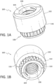
- FIGs. 1A-1D illustrate top perspective, bottom perspective, side, and cross-sectional views of a clinch nut 100.
- the clinch nut 100 includes a head 102 and insert 108.
- the head 102 has an opening 104 with threads 106.
- the opening 104 is intended to receive a screw so that various components may be connected to the clinch nut 100 and hence the PCB. Further, as the clinch nut 100 is conductive, this proves an electrical connection between the component and the PCB. This may be used for grounding a component such as, for example, a heat sink.
- the head 102 has a head outer surface 116.
- the head 102 has a head bottom surface 114 that may come into contact with a conductive layer or pad on the PCB to provide the electrical connectivity.
- the head 102 is illustrated as being cylindrical, but other shapes may be used as well.
- the insert 108 extends from the head 102 and is intended to enter a through hole on the PCB and to engage the through hole to secure the clinch nut 100 to the PCB.
- the insert 108 may include ridges 110 that grip the through hole in order to facilitate a secure connection between the clinch nut 100 and the PCB.
- the ridges 110 may take any shape that facilitates a secure engagement of the insert 108 with the through hole of the PCB. In some situations the insert 108 may not have the ridges 110, but instead will be sized and shaped to securely engage the through hole.
- the insert 108 is illustrated as being generally cylindrical, but other shapes may be used as long as they conform with and are complementary to the shape of the through hole in the PCB. Further, the ridges 110 may not extend along the length of the insert 108 as illustrated so that there is a gap 112 between the ridges 110 and the head bottom surface 114.
- the clinch nut 100 may come in various lengths and diameters depending on the specific application.
- the length of the head 102 will be sized to provide distance between the component attached to the clinch nut 100 and the PCB. Further, the length of the insert 108 will be based upon the thickness of the PCB. In some situations the clinch nut 100 may be double sided so that the insert 108 may extend through the through hole in the PCB and provide a connection point on the other side of the PCB.
- FIGs. 2A and 2B illustrate a side and cross-sectional view of the clinch nut 100 inserted into a through hole 206 of the PCB 202.
- the PCB 202 includes a conductive pad 204 that surrounds the through hole 206 at the surface of the PCB 202.
- the head bottom surface 114 comes into contact with the conductive pad 204.
- the ridges 110 of the insert 108 engage an inner surface of the through hole 206 so that the clinch nut 100 is securely attached to the PCB 202.
- FIG. 2C illustrates a cross-sectional view of the clinch nut 100 inserted into the through hole 206, but with a gap 212 between the head bottom surface 114 and the conductive pad 204.
- the gap 212 between the head bottom surface 114 and the conductive pad 204 may occur.
- One way is when the clinch nut 100 is pressed into the PCB 202 and the layers of the PCB 202 are compressed, and then when the die used by the press is removed from the clinch nut 100, the compressed layers of the PCB 202 relax causing the clinch nut 100 to move slightly out of the through hole 206. This can cause the gap 212 to occur.
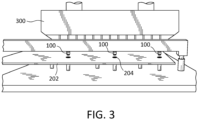
- FIG. 3 illustrates a press 300 pressing in multiple clinch nuts 100 into the PCB 202 at the same time.
- Embodiments using a solder layer will now be described that overcome these problems.
- the embodiment using solder is relatively simple to implement, and the benefits are numerous.
- This embodiment includes a reflowed solder layer, either over the full clinch nut footprint or in selected regions.
- the solder layer may be added at the reflow or wave stage during PCB processing.
- the standard solder paste stencil may be modified to accommodate an aperture for the clinch nut head footprint.
- the wave solder fixture may have an opening to allow solder to wet the conductive pad 204.
- the clinch nuts 100 are pressed into the designated through holes 206 on the PCB 202.
- the solder is meant to make contact with the head 102. This solder acts as a contact point for the clinch nut 100 and is not soldered to the clinch nut 100 itself.
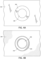
- FIG. 4A illustrates a top view of the conductive pad 204 and through hole 206 on the PCB 202.
- FIG. 4B illustrates the use of a solder mask 208 to facilitate the placement of solder 210 on the conductive pad 204.
- the solder 210 is placed all around the conductive pad 204.
- FIGs. 4C and 4D illustrate solder 210 being placed in four and two separate locations around the conductive pad 204, respectively.
- the embodiments of FIGs. 4C and 4D mean less solder is used and may result in faster processing.
- Solder may be placed in one or more locations on the conductive pad 204 and the amount of solder placed is chosen to ensure that the clinch nut 100 will be reliably electrically connected to the conductive pad 204. Further, the thickness of the solder 210 is selected to ensure that the solder 210 connects the clinch nut 100 to the conductive pad 204 in light of the tolerances of the clinch nut 100.
- PCBs require a layer less reactive to environmental contaminants coating exposed copper surfaces. This delays the effects of airborne atoms and compounds from tarnishing the copper surface, thus preserving the copper's solderability for greater lengths of time than without any additional coating or treatment.
- Common surface treatments or finishes include electroless nickel immersion gold (ENIG), immersion silver, immersion tin, organic solderability preserve and hot air solder levelling (HASL), but many other finishes exist. Soldering processes are typically completed on finished copper surfaces, and may evaporate, dissolve, or plate over the finished materials.
- HASL finish which is preemptively soldering un-tarnished bare copper to prevent tarnishing rather than finishing it with an alternate barrier layer.
- HASL will typically be thinner than an additional solder layer, and less precisely controlled.
- HASL is uncommon to use on products within the telecommunications industry, and poorly suited to most fine pitch interconnect applications.
- a lab can distinguish between HASL and the embodiments described herein on a customer product by the height of the additional solder layer, whether all outer layer copper on the PCB has a somewhat uniformly thick coating of solder, and/or whether there are additional metals in the solder joint representative of the surface finish used.
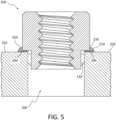
- FIG. 5 illustrates a cross-sectional view of the clinch nut 100 inserted in the through hole 206 of the PCB 202 with the solder 210 between the head bottom surface 114 and the conductive pad 204.
- a plot of this relationship shows a fairly linear slope to a plot of distance verses the force applied, until the clinch nut 100 comes into contact with the PCB 202, at which point the slope of this plot becomes almost vertical. This change in the slope may be monitored and indicate to the press that the clinch nut 100 is seated.
- the solder 210 will fill any remaining gaps between the head bottom surface 114 and the conductive pad 204. This will result in electrical connectivity between the clinch nut 100 and the conductive pad 204 and hence between the component attached to the clinch nut 100 and the PCB 202.
- the solder 210 further helps when there is slight relaxation of the PCB 202 that causes the clinch nut 100 to move out of the through hole 206, because parts of the 210 will still maintain contact with the head 102 of the clinch nut 100 to preserve electrical connectivity.
- solder aims to: act as a sacrificial layer to minimize the damage on the PCB 202 inner layers inherent to the clinch nut process; act as a point to electrically connect the clinch nut 100 to the PCB 202; and accommodate for the pressing of multiple clinch nuts 100 at once by planning for the solder 210 to be compressed completely out from between the clinch nut 100 and the conductive pad 204, and accounting for the other clinch nuts 100 to still make physical contact with the partially compressed solder 210 to preserve electrical connectivity.
- solder 210 may be placed on the conductive pads 204 around through holes 206 that will receive clinch nuts 100. This may be done by placing a solder mask over the PCB 202 and placing solder where it is needed. This may be done during the reflow state of manufacturing the PCB 202. If wave soldering is being used, then this may be done during the wave solder stage. Next, one or more clinch nuts 100 are loaded onto a die and then pressed into the PCB using a press.
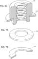
- FIGs. 6A-6C illustrate the use of a washer 118 with the clinch nut 100.
- the washer 118 may be captured in the gap 112 between the ridges 110 and the head bottom surface 114. In other embodiments where there are no ridges 110, the washer 118 may still be used, but is not captured on the clinch nut 100.
- the washer 118 is illustrated as being a conical washer.
- the conical washer may have its concave side towards the PCB 202 (as illustrated in FIGs. 6A-6C ) or towards the clinch nut 100 (not shown).
- FIGs. 7A and 7B illustrate a top perspective and cross-sectional view of the washer 118.
- the washer 118 has a slightly conical shape that allows for some compression when used with the clinch nut 100. As a result, the washer 118 can also prevent any break in electrical connectivity between the clinch nut 100 and the PCB 202.
- the washer 118 may be flat, but may be made of a soft and/or malleable compressible material that allows for compression when the clinch nut 100 is pressed against the washer 118. This may compensate for variations in the tolerances of the clinch nuts 100.
- the washer 118 may be a split washer, i.e., the washer has a break and the ends of the break are offset from one another. This washer design allows for variations in compression between the head bottom surface 114 and the conductive pad 204, and it will facilitate maintaining electrical connectivity between multiple clinch nuts 100 and the conductive pads 204.
Landscapes
- Engineering & Computer Science (AREA)
- Microelectronics & Electronic Packaging (AREA)
- Manufacturing & Machinery (AREA)
- Metallurgy (AREA)
- Electric Connection Of Electric Components To Printed Circuits (AREA)
- Coupling Device And Connection With Printed Circuit (AREA)
Applications Claiming Priority (1)
| Application Number | Priority Date | Filing Date | Title |
|---|---|---|---|
| US18/174,031 US20240292546A1 (en) | 2023-02-24 | 2023-02-24 | Sacrificial solder layer for broaching clinch nut assembly |
Publications (2)
| Publication Number | Publication Date |
|---|---|
| EP4422362A2 true EP4422362A2 (de) | 2024-08-28 |
| EP4422362A3 EP4422362A3 (de) | 2024-10-09 |
Family
ID=89977962
Family Applications (1)
| Application Number | Title | Priority Date | Filing Date |
|---|---|---|---|
| EP24157949.9A Withdrawn EP4422362A3 (de) | 2023-02-24 | 2024-02-15 | Opferlotschicht zum räumen einer krimpmutteranordnung |
Country Status (3)
| Country | Link |
|---|---|
| US (1) | US20240292546A1 (de) |
| EP (1) | EP4422362A3 (de) |
| CN (1) | CN118555730A (de) |
Family Cites Families (6)
| Publication number | Priority date | Publication date | Assignee | Title |
|---|---|---|---|---|
| JPH05243756A (ja) * | 1992-03-02 | 1993-09-21 | Nec Corp | 電子部品用アセンブリー |
| US7518384B2 (en) * | 2005-01-31 | 2009-04-14 | Agilent Technologies, Inc. | Method and apparatus for manufacturing and probing test probe access structures on vias |
| US20080146092A1 (en) * | 2006-12-14 | 2008-06-19 | William Fillmore Taylor | Printed circuit board connection |
| JP4746703B1 (ja) * | 2010-03-29 | 2011-08-10 | 株式会社東芝 | 電子機器、ハードディスクドライブ |
| DE102016212528B4 (de) * | 2015-07-15 | 2022-05-05 | Denso Corporation | Elektronische Vorrichtung |
| DE102021203723A1 (de) * | 2021-04-15 | 2022-04-21 | Carl Zeiss Smt Gmbh | Verbindungsanordnung, projektionsbelichtungsanlage und verfahren |
-
2023
- 2023-02-24 US US18/174,031 patent/US20240292546A1/en not_active Abandoned
-
2024
- 2024-02-15 EP EP24157949.9A patent/EP4422362A3/de not_active Withdrawn
- 2024-02-22 CN CN202410198831.8A patent/CN118555730A/zh active Pending
Also Published As
| Publication number | Publication date |
|---|---|
| CN118555730A (zh) | 2024-08-27 |
| EP4422362A3 (de) | 2024-10-09 |
| US20240292546A1 (en) | 2024-08-29 |
Similar Documents
| Publication | Publication Date | Title |
|---|---|---|
| US4872261A (en) | Method of and apparatus for surface mounting electronic components onto a printed wiring board | |
| US7151229B2 (en) | Printed circuit board with improved cooling of electrical component | |
| US9711876B2 (en) | Clamping spring | |
| EP1350417B1 (de) | Verfahren zur herstellung einer elektronischen baugruppe | |
| WO2001049088A1 (en) | Direct bga attachment without solder reflow | |
| US2915678A (en) | Electrical mounting devices | |
| EP0947125B1 (de) | Verfahren zum herstellen einer leiterplatteranordnung mit zinn/bleischicht | |
| JP2006186136A (ja) | 両面部品実装回路基板及びその製造方法 | |
| JPH10513308A (ja) | 電気伝導ワイヤ | |
| US6095400A (en) | Reinforced solder preform | |
| EP4422362A2 (de) | Opferlotschicht zum räumen einer krimpmutteranordnung | |
| US20090284939A1 (en) | Alignment plate | |
| US6087596A (en) | Solder joints for printed circuit boards having intermediate metallic member | |
| US6493238B1 (en) | Method and apparatus to compliantly interconnect area grid arrays and printed wiring boards | |
| US20070127218A1 (en) | Electronic apparatus and method of manufacturing the same | |
| US6580613B2 (en) | Solder-free PCB assembly | |
| US6182883B1 (en) | Method and apparatus for precisely registering solder paste in a printed circuit board repair operation | |
| US6168976B1 (en) | Socketable BGA package | |
| US11310919B2 (en) | Method for producing a connection contact | |
| RU2859184C1 (ru) | Способ установки медных шин на печатную плату с электронными компонентами методом клёпки с пайкой | |
| CN115279059B (zh) | 一种小间距波峰物料及其焊接方法 | |
| US20070184688A1 (en) | Interconnection device for a double-sided printed circuit board | |
| JP2002076564A (ja) | 半田クラック防止用スリーブ | |
| KR20030073058A (ko) | 비지에이 또는 엘지에이 소자의 인쇄 회로 주기판 무납땜장착 및 분리를 위한 장치. | |
| US20060037778A1 (en) | Circuit board with SMD-components and at least one wired component, and a method for populating, securing and electrical contacting of the components |
Legal Events
| Date | Code | Title | Description |
|---|---|---|---|
| PUAI | Public reference made under article 153(3) epc to a published international application that has entered the european phase |
Free format text: ORIGINAL CODE: 0009012 |
|
| STAA | Information on the status of an ep patent application or granted ep patent |
Free format text: STATUS: THE APPLICATION HAS BEEN PUBLISHED |
|
| AK | Designated contracting states |
Kind code of ref document: A2 Designated state(s): AL AT BE BG CH CY CZ DE DK EE ES FI FR GB GR HR HU IE IS IT LI LT LU LV MC ME MK MT NL NO PL PT RO RS SE SI SK SM TR |
|
| PUAL | Search report despatched |
Free format text: ORIGINAL CODE: 0009013 |
|
| AK | Designated contracting states |
Kind code of ref document: A3 Designated state(s): AL AT BE BG CH CY CZ DE DK EE ES FI FR GB GR HR HU IE IS IT LI LT LU LV MC ME MK MT NL NO PL PT RO RS SE SI SK SM TR |
|
| RIC1 | Information provided on ipc code assigned before grant |
Ipc: H01R 12/51 20110101ALI20240905BHEP Ipc: H05K 3/32 20060101ALI20240905BHEP Ipc: H05K 1/11 20060101AFI20240905BHEP |
|
| STAA | Information on the status of an ep patent application or granted ep patent |
Free format text: STATUS: THE APPLICATION IS DEEMED TO BE WITHDRAWN |
|
| 18D | Application deemed to be withdrawn |
Effective date: 20250410 |